JP2004166380A - Electric shock preventive circuit for on-vehicle ground insulation circuit - Google Patents
Electric shock preventive circuit for on-vehicle ground insulation circuit Download PDFInfo
- Publication number
- JP2004166380A JP2004166380A JP2002328657A JP2002328657A JP2004166380A JP 2004166380 A JP2004166380 A JP 2004166380A JP 2002328657 A JP2002328657 A JP 2002328657A JP 2002328657 A JP2002328657 A JP 2002328657A JP 2004166380 A JP2004166380 A JP 2004166380A
- Authority
- JP
- Japan
- Prior art keywords
- circuit
- ground
- power supply
- circuit unit
- electric shock
- Prior art date
- Legal status (The legal status is an assumption and is not a legal conclusion. Google has not performed a legal analysis and makes no representation as to the accuracy of the status listed.)
- Granted
Links
Images

Abstract
Description
【0001】
【発明が属する技術分野】
本発明は、車載対地絶縁回路用感電防止回路に関する。
【0002】
【従来の技術】
車載の高圧バッテリ(たとえば数百V)から給電される直流電力を三相交流電力に変換して三相交流モータなどの負荷に給電する車載インバータ回路では、安全性などの点から回路全体は、一般に車体から絶縁されている。
【0003】
この種の回路における感電防止回路として、下記特許文献1、2は、三相モータのいわゆるCT(カレントトランスホーマー)すなわちピックアップコイルにより回路の零相交流電流成分を検出し、検出したこの零相交流電流成分をキャンセルする電流を回路に流すことを提案している。
【0004】
【特許文献1】特開平9−215341号公報
【特許文献2】特開平10−42585号公報
【0005】
【発明が解決しようとする課題】
しかしながら、上記した従来の感電防止回路は、零相交流電流成分検出のためのピックアップコイルが大型となってしまうため装置の必要スペース、重量の増大による車両搭載性の悪化、製造コストの増大が生じ、その結果として車両用として実用化することが困難となっていた。
【0006】
また、ピックアップコイルは種々の外部雑音磁界を拾い易いので、それを実用レベルまで防止するためには大型の磁気シールド部材の設置が必須となり、その結果としてますます車両搭載性が低下した。
【0007】
本発明は上記問題点に鑑みなされたものであり、小型軽量で車載性、経済性に優れた対地絶縁回路用感電防止回路を提供することをその目的としている。
【0008】
【課題を解決するための手段】
請求項1記載の車載対地絶縁回路用感電防止回路は、直流電圧を交流電圧に変換するインバータ回路部と、前記インバータ回路の交流出力端子から出力される交流電圧が印加される負荷回路部と、前記インバータ回路の一対の直流入力端子間に直流電圧を印加する電源回路部とを有して車体に対し電気絶縁される車載対地絶縁回路に設けられて、前記電源回路部への人体接触時の感電電流を低減する車載対地絶縁回路用感電防止回路において、
前記電源回路部の所定点の対地交流電位変動を検出する対地交流電位変動検出回路部と、前記対地交流電位変動検出回路部が検出した前記対地交流電位変動に基づいて前記電源回路部の所定点の対地交流電位変動を抑制する抑制回路部とを備えることを特徴としている。
【0009】
これにより、小型かつ軽量で車両搭載性に優れた装置により精度よく電源回路部の対地交流電位変動による交流感電電流を抑制することができる。
【0010】
以下、バッテリを含む電源回路部から給電される直流電力をインバータ回路部で交流電力に変換して交流負荷(たとえば交流モータ)を含む負荷回路部に供給する車載対地絶縁回路を例として更に詳しく説明する。電源回路部、インバータ回路部及び負荷回路部はそれぞれ浮遊容量を通じて車体に接続されている。この種の回路では、交流モータの内部の浮遊容量増大が生じることがあるので、もし人体がたとえば電源回路部の所定点に接触すると、この浮遊容量、車体、人体、電源回路部、インバータ回路部、負荷回路部、この浮遊容量を循環する電流ループが形成されて、人体に大きな交流感電電流が流れる。人体にこのような大きな交流電流が流れるということは、電源回路部の上記所定点又はその他の各部の対地交流電位変動が大きくなることを意味する。たとえば、人体が電源回路部の低位直流電源ラインに接触している場合、人体を流れる交流感電電流をiac、人体抵抗をrとすれば、低位直流電源ラインの対地交流電位変動ΔVはiac・rとなる。
【0011】
そこで、この発明では、電源回路部の所定点たとえば低位直流電源ラインの対地交流電位変動を交流電位変動検出回路部により検出し、この検出信号に基づいて電源回路部の所定点たとえば低位直流電源ラインの対地交流電位変動を抑制回路部により抑制する。当然、この対地交流電位変動ΔVの抑制は、上記式から人体を流れる交流感電電流iacの抑制に相当する。この抑制回路部による抑制は、人体を通じて本来流れる筈の交流電流を抑制回路部を通じて迂回させることを意味する。
【0012】
したがって、この発明によれば、従来のように、大型高ターンで外部ノイズ磁界も拾いやすいループコイルを用いることなく、小型かつ軽量で車両搭載性に優れた装置により精度よく交流感電を防止することができる。
【0013】
好適な態様において、前記対地交流電位変動検出回路部は、検出コンデンサと抵抗素子とを直列接続してなるCR直列回路を有し、前記検出コンデンサの一端は前記電源回路部の前記所定点に接続され、前記抵抗素子の一端は車体に接地され、前記検出コンデンサ及び抵抗素子の両他端は接続されて出力点をなすので、検出コンデンサにより電源回路部が車体に直流絶縁を確保しつつ、電源回路部の所定点の交流電位変動のみを抵抗素子により検出することができる。なお、このCR直列回路において、抵抗素子の電圧降下は上記所定点の交流電位変動の分圧となるので、検出コンデンサの容量を増大することにより、検出回路部の出力電圧を増大することができる。抵抗素子は本質的に他のインピーダンス素子としてもよい。たとえば、コンデンサとしてもよく、非線形インピーダンス素子としてもよい。また、この検出回路部の出力電圧をオペアンプなどにより電圧増幅して次段の抑制回路部に出力しても良い。
好適な態様において、前記抑制回路部は、前記電源回路部の高位直流電源ラインと低位直流電源ラインとから給電されて前記検出回路部の前記出力点から入力信号電圧を受け取るコンプリメンタリエミッタホロワ回路又はコンプリメンタリソースホロワ回路と、一端が前記コンプリメンタリエミッタホロワ回路又はコンプリメンタリソースホロワ回路の出力接点に、他端が車体に接続された抑制コンデンサとを有するので、簡単な回路構成により電源回路部の所定点の交流電位変動を抑制することができる。なお、電源回路部の所定点の交流電位変動を抑制すれば、電源回路部の他の交流電位変動も抑制することができる。
【0014】
また、コンプリメンタリエミッタホロワ回路やコンプリメンタリソースホロワ回路のトランジスタは、入力電圧変動にほぼ等しい出力電圧変動を形成できるうえ、電源回路部の直流電圧が抑制コンデンサに印加されるのを防止することができるため、抑制コンデンサの耐電圧を大幅に小さくすることができる。
【0015】
好適な態様において、前記対地交流電位変動検出回路部及び/又は前記抑制回路部は、前記電源回路部から前記対地交流電位変動検出回路部及び/又は前記抑制回路部を通じて車体に流れる所定レベル以上の直流電流を遮断乃至寄生する直流電流遮断素子、たとえばヒューズや電流制限抵抗を有するので、たとえコンデンサやトランジスタが短絡故障を起こしても、車体に直流電流が流れるのを防止することができる。
【0016】
好適な態様において、前記電源回路部の所定点の対地直流電位変動を検出する対地直流電位変動検出回路部と、前記対地直流電位変動検出回路部の出力信号電圧に基づいて前記所定点の直流電位変動が所定レベルを超えた場合にのみ前記抑制回路部の作動を許可する許可回路部とを有する。これにより、人体などの直流インピーダンス体が電源回路部に接触した場合のみ、抑制回路部を作動させることができるので、常時抑制回路部を作動させる場合に比較して電力消費を低減することができる。
【0017】
この効果を更に説明する。
【0018】
たとえば250Vの直流電位差をもつ電源回路部の高位直流電源ライン及び低位直流電源ラインが略等しい浮遊容量を通じて接地されているとすれば、車体(DC0V)を基準として高位直流電源ラインは+125V、低位直流電源ラインはー125Vとなる筈である。電気抵抗値が非常に小さい(通常数百V)人体が低位直流電源ラインに接触すれば低位直流電源ラインの対地直流電位は略0Vにレベルアップし、高位直流電源ラインに接触すれば、低位直流電源ラインの対地直流電位は略ー250Vに低下する。人体が高位直流電源ラインに接触する場合にも、人体が高位直流電源ラインに接触する場合の高位直流電源ライン又は低位直流電源ラインの対地直流電位変動も同様である。
【0019】
したがって、高位直流電源ライン又は低位直流電源ラインの対地直流電位変動が所定しきい値を超えれば、人体又は同様の直流インピーダンスをもつ電気抵抗体がこれら高位直流電源ライン又は低位直流電源ラインに接触したと判定することができる。そこで、この判定結果により人体が高位直流電源ライン又は低位直流電源ラインに接触した場合にだけ抑制回路部を作動させるようにすれば、抑制回路部の電力消費を低減することができる。
【0020】
【発明の実施の形態】
本発明の感電防止回路を図面を参照して説明する。
(実施例1)
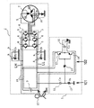
実施例1の回路を図1の回路図を参照して説明する。図1は、電気自動車の走行モータ駆動回路を示している。
(回路構成)
図1において、1は感電防止回路、2は走行モータ駆動回路である。
【0021】
走行モータ駆動回路2は、バッテリ(電源回路部)3、インバータ回路部4、三相交流モータ(負荷回路部)5からなる。感電防止回路1は、対地交流電位変動検出回路部101と、抑制回路部102とからなる。
【0022】
バッテリ3とインバータ回路部4とを接続する高位直流電源ラインLH及び低位直流電源ラインLLは、本発明で言う電源回路部に属する。インバータ回路部4は、6個のIGBT6と、各IGBT6に個別に逆並列接続されたフライホイルダイオードを有する周知の三相インバータ回路からなる。負荷回路部5は、三相交流モータ5とインバータ回路部22の3つの交流出力端とを接続する3本の交流ライン(符号省略)を含む。
【0023】
対地交流電位変動検出回路部101は、検出コンデンサ11と抵抗素子12とを直列接続してなるCR直列回路からなり、検出コンデンサ11の一端は低位直流電源ラインLLに、抵抗素子12の一端は車体に、両者の接続点は出力点を構成している。
【0024】
抑制回路部102は、ベース電流制限抵抗16、エミッタホロワトランジスタ13、14、抑制コンデンサ15からなる。エミッタホロワ接続されたトランジスタ13、14は、コンプリメンタリエミッタホロワ回路を構成しており、トランジスタ13のコレクタは高位直流電源ラインLHに、トランジスタ14のコレクタは低位直流電源ラインLLに、トランジスタ13、14のベースは抵抗16を通じて検出コンデンサ11と抵抗素子12との接続点に、トランジスタ13、14のエミッタは抑制コンデンサ15を通じて車体に接地されている。
【0025】
8は高位直流電源ラインLH、低位直流電源ラインLLの対地絶縁抵抗、9は高位直流電源ラインLH、低位直流電源ラインLLの対地浮遊容量、10は三相交流モータ5の三相ステータコイル7の一つとモータハウジング(車体接地)との間との浮遊容量、17は低位直流電源ラインLLに接触した人体である。
【0026】
対地絶縁抵抗8の電気抵抗値はRb、対地浮遊容量9の容量値はCb、検出コンデンサ11の容量値はCa、抵抗素子12の抵抗値はRa、抑制コンデンサ15の容量値はCc、浮遊容量10の容量値はCmに設定されている。19はコンプリメンタリエミッタホロワ回路を構成するトランジスタ13、14を通じて流れる交流電位変動抑制のための電流を示す。
【0027】
(動作説明)
次に、人体17が低位直流電源ラインLLに接触し、浮遊容量10の容量値Cmが他の容量に比較して大きくなり、人体抵抗と浮遊容量10とを通じて流れる対地交流電流の低減について以下に説明する。
【0028】
既述したように、低位直流電源ラインLLの交流電位変動をΔV、人体17の電気抵抗をrとした場合において人体17を通じて流れる交流感電電流iacは、ΔV/rとなる。すなわち、交流感電電流iacを低減するには、低位直流電源ラインLLの対地交流電位変動ΔVを低減すればよい。
【0029】
検出コンデンサ11と抵抗素子12とからなるCR直列抵抗回路には上記対地交流電位変動ΔV及び対地直流電位変動成分とが印加されるが対地直流電位変動成分は検出コンデンサ11により負担され、抵抗素子12の両端には上記した対地交流電位変動ΔVの分圧が印加される。検出コンデンサ11の交流インピーダンスが抵抗素子12の抵抗値に比較して十分にちいさければ、対地交流電位変動ΔVのほとんどは抵抗素子12の電圧降下となる。抵抗素子12の電圧降下は、ベース電流抵抗素子16を通じてコンプリメンタリエミッタホロワ回路のトランジスタ13、14に印加され、トランジスタ13、14の交互オンにより上記した電流19が流れて抑制コンデンサ15が充放電されて、低位直流電源ラインLL及び高位直流電源ラインLHの対地交流電位変動が抑制される。
【0030】
この対地交流電位変動ΔVの抑制について更に詳しく説明する。なお、この対地交流電位変動ΔVのうちでインバータ回路部4のキャリヤ周波数成分が最も大きいが、その高調波成分も当然存在する。
【0031】
まず、対地交流電位変動ΔVにより低位直流電源ラインLLの電位がその対地直流電位レベルよりも高くなる期間における抑制について図2に示す模式回路を参照して以下に説明する。
【0032】
図2では、簡単化のために、インバータ回路部4を単相インバータ回路、負荷回路部5を単相交流負荷とし、かつ高位直流電源ラインLH及び低位直流電源ラインLLの浮遊インピーダンスを相対的に小さいとして無視し、対地直流電位変動検出回路部101は低位直流電源ラインLLの対地交流電位変動ΔVを検出するものとする。したがって、インバータ回路部4で形成される交流電圧は負荷回路部5の大きな浮遊容量10、車体、人体抵抗17、電源回路部、インバータ回路部4を通じて環流するものとする。61〜64はインバータ回路部4の4つのスイッチング素子であるとする。
【0033】
まず、浮遊容量10が充電される半周期について説明する。この時、浮遊容量10はスイッチング素子63を通じて充電され、低位直流電源ラインLLには人体抵抗17を通じて車体から電流が流れ込むため、配線抵抗やスイッチング素子61〜64などの抵抗を無視すれば、人体抵抗17の電圧降下は浮遊容量10の電圧に等しくなり、低位直流電源ラインLLの対地電位は車体電位すなわち接地電位(0V)よりも低下する。低位直流電源ラインLLのこの対地電位低下により、検出回路部101の出力電圧は低下するが、検出回路部101の出力電圧が抑制コンデンサ15の端子電圧の電位ー約0.7Vとなればトランジスタ14がオンし、抑制コンデンサ15に蓄積されていた電荷がトランジスタ14を通じて低位直流電源ラインLLに放出され、低位直流電源ラインLLの電位低下が抑制され、これにより人体抵抗17を流れる電流が減少する。検出回路部101の出力電圧が最終的にV1まで低下する場合、抑制コンデンサ15の端子電圧はV1+約0.7V程度までその放電は行われる。
【0034】
次に、浮遊容量10が放電する次の半周期について説明する。この時、浮遊容量10はスイッチング素子62を通じて放電し、低位直流電源ラインLLから人体抵抗17を通じて車体に電流が流れ出るため、配線抵抗やスイッチング素子61〜64などの抵抗を無視すれば、人体抵抗17の電圧降下は浮遊容量10の電圧に等しくなり、低位直流電源ラインLLの電位は車体電位すなわち接地電位(0V)よりも上昇する。低位直流電源ラインLLのこの対地電位上昇により、検出回路部101の出力電圧は低下するが、検出回路部101の出力電圧が抑制コンデンサ15の端子電圧の電位+約0.7Vとなればトランジスタ13がオンし、抑制コンデンサ15は高位直流電源ラインLHからトランジスタ13を通じて充電される。高位直流電源ラインLHの交流電位は低位直流電源ラインLLのそれと等しいとみなすことができるので、低位直流電源ラインLLの電位は低下する。言い換えれば、浮遊容量10から低位直流電源ラインLLに放電された電荷はバッテリ3、高位直流電源ラインLH、トランジスタ13を通じて抑制コンデンサ15に吸収され、抑制コンデンサ15は充電され、その分だけ人体抵抗17を流れる電流が低下する。検出回路部101の出力電圧が最終的にV2になるとすると、抑制コンデンサ15の端子電圧はV2ー約0.7V程度までこの充電は行われる。
【0035】
上記作用により、人体抵抗17を流れる交流感電電流を大幅に低減することができる。なお、図2においては検出回路部101を低位直流電源ラインLLと車体との間に配置したが、低位直流電源ラインLLと高位直流電源ラインLHとは交流的に等価であり、検出回路部101を高位直流電源ラインLHに接続してもよいことは当然である。また、バッテリ3内の一点に接続しても良い。
【0036】
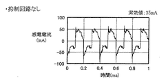
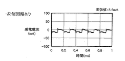
実験例を図3、図4に示す。図3は図1の回路において感電防止回路1を外した場合の人体抵抗17(700オームの抵抗素子で代用)を流れる感電電流を示し、図4は感電防止回路1を取り付けた場合のそれを示す。なお、感電電流はインバータ回路部4の搬送周波数の逆数を周期とする交流電流波形となるが、各周期の最初においてトランジスタ13、14のオン遅れに伴うサージ(スパイク)電流成分が存在する。しかし、このサージ電流の周波数を高く、人体において感電電流の周波数が高くなるほど表皮効果によりそれは人体の表面部を流れるため、大きな問題とはならない。
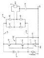
(実施例2)
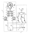
図5に示すこの実施例は、図1において、感電防止回路1に、人体接触検出回路部103を追加したものである。
【0037】
(回路構成)
人体接触検出回路部103は、低位直流電源ラインLLの対地直流電位変動を検出する対地直流電位変動検出回路部104と、対地直流電位変動検出回路部104の出力信号電圧に基づいて低位直流電源ラインLLの直流電位変動が所定レベルを超えた場合にのみ抑制回路部102の作動を許可するアナログスイッチ(本発明で言う許可回路部)105とからなる。
【0038】
対地直流電位変動検出回路部104は、互いに直列接続されて全体として高合成抵抗値を有する抵抗素子20、21からなる抵抗分圧回路と、この抵抗分圧回路の出力電圧を定電圧電源23の出力電圧である参照電圧Vrefとを比較する二つのコンパレータ221、222と、これら二つのコンパレータ221、222の出力電圧の論理和信号を出力するオア回路(図示せず)とを有し、このオア回路はアナログスイッチ105のゲート電極を制御している。コンパレータ221、222はいわゆるウインドコンパレータとして機能する。なお、25はアナログスイッチ105がオフした場合におけるコンプリメンタリエミッタホロワ回路のオフ動作を速やかにするための放電抵抗であるが、省略しても差し支えない。なお、抵抗20、21の合成抵抗は電力消費を無視できる程度に設定することが好ましい。
【0039】
(動作説明)
この回路の動作を以下に説明する。バッテリ3は250Vとする。
【0040】
まず、人体が高位直流電源ラインLH及び低位直流電源ラインLLに接触していない場合を説明する。この場合には、高位直流電源ラインLHの対地交流インピーダンスと低位直流電源ラインLLのそれとは略等しいとみなすことができるため、高位直流電源ラインLHは略+125V、低位直流電源ラインLLは略ー125Vの対地直流電位をもち、この低位直流電源ラインLLの対地直流電位の分圧Vxは、参照電圧ーVrefよりも正で、参照電圧+Vrefよりも負とする。これにより、二つのコンパレータ221、222はともにローレベルを出力し、図示しないオア回路はアナログスイッチ105をオフする。これにより抑制回路部102は作動せず、その電力消費は生じない。
【0041】
次に、人体が低位直流電源ラインLLに接触した場合を説明する。この場合には、低位直流電源ラインLLは低抵抗を通じて対地にアースされるために、低位直流電源ラインLLの対地直流電位は略0Vまで上昇し、コンパレータ221がハイレベルを出力し、アナログスイッチ105がオンし、抑制回路部102が作動する。
【0042】
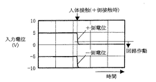
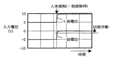
次に、人体が高位直流電源ラインLHに接触した場合を説明する。この場合には、高位直流電源ラインLHは低抵抗を通じて対地にアースされるために、高位直流電源ラインLHの対地直流電位は略0Vまで上昇し、低位直流電源ラインLLの対地直流電位は略ー250Vまで低下し、コンパレータ222がハイレベルを出力し、アナログスイッチ105がオンし、抑制回路部102が作動する。図6は、人体が高位直流電源ラインLHに接触した場合の高位直流電源ラインLHの対地直流電位(+側電位として表示)及び低位直流電源ラインLLの対地直流電位(ー側電位として表示)の変動を示し、図7は、人体が低位直流電源ラインLLに接触した場合の高位直流電源ラインLHの対地直流電位(+側電位として表示)及び低位直流電源ラインLLの対地直流電位(ー側電位として表示)の変動を示す。結局、この実施例によれば、人体が高位直流電源ラインLH及び低位直流電源ラインLLを含む電源回路部に接触した場合にだけ抑制回路部102を作動させることにより、電力消費を節減することができる。
【0043】
(実施例3)
図8に示すこの実施例は、図1において、感電防止回路1に、充電電流制限抵抗26、放電抵抗制限抵抗27、ヒューズ28〜30を追加したものである。これら回路素子は、本発明で言う直流電流遮断素子であって、トランジスタ13、14や抑制コンデンサ15の短絡故障が生じた場合の短絡電流を制限又は遮断を行うので、回路安全性を向上することができる。
【0044】
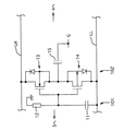
(実施例4)
実施例4の回路を図9に示す。図9の回路は、図1に示す抑制回路部102のコンプリメンタリエミッタホロワ回路をコンプリメンタリソースホロワ回路に変更したものであるが、動作は実質的に同じである。
【図面の簡単な説明】
【図1】実施例1の回路を示す回路図である。
【図2】実施例1の回路動作を説明するための模式回路図である。
【図3】実施例1の抑制回路部を用いない場合における人体感電電流の波形を示す波形図である。
【図4】実施例1の抑制回路部を用いる場合における人体感電電流の波形を示す波形図である。
【図5】実施例2を示す回路図である。
【図6】実施例2における人体接触による対地直流電位変動を示す波形図である。
【図7】実施例2における人体接触による対地直流電位変動を示す波形図である。
【図8】実施例3を示す回路図である。
【図9】実施例4を示す回路図である。
【符号の説明】
1は感電防止回路、2は走行モータ駆動回路、3はバッテリ(電源回路部の一部)、4はインバータ回路部、5は三相交流モータ(負荷回路部)、101は対地交流電位変動検出回路部、102は抑制回路部102、LHは高位直流電源ライン、LLは低位直流電源ライン、6はIGBT、11は検出コンデンサ、12は抵抗素子、13、14はエミッタホロワトランジスタ、15は抑制コンデンサ15、10は浮遊容量、17は人体、103は人体接触検出回路部、104は対地直流電位変動検出回路部、105はアナログスイッチ(本発明で言う許可回路部)105である。[0001]
TECHNICAL FIELD OF THE INVENTION
The present invention relates to an electric shock prevention circuit for a vehicle-mounted ground insulation circuit.
[0002]
[Prior art]
In a vehicle-mounted inverter circuit that converts DC power supplied from a vehicle-mounted high-voltage battery (for example, several hundred volts) into three-phase AC power and supplies the power to a load such as a three-phase AC motor, the entire circuit is safety-related. Generally insulated from the vehicle body.
[0003]
As an electric shock prevention circuit in this type of circuit,
[0004]
[Patent Document 1] Japanese Patent Application Laid-Open No. 9-215341 [Patent Document 2] Japanese Patent Application Laid-Open No. 10-42585 [0005]
[Problems to be solved by the invention]
However, in the above-described conventional electric shock prevention circuit, the pickup coil for detecting the zero-phase alternating current component becomes large, so that the space required for the device, the mountability of the vehicle due to the increase in weight, and the increase in manufacturing cost occur. As a result, it has been difficult to put it to practical use for vehicles.
[0006]
Further, since the pickup coil easily picks up various external noise magnetic fields, it is necessary to install a large magnetic shield member in order to prevent the magnetic field from reaching a practical level, and as a result, the mountability on a vehicle is further reduced.
[0007]
The present invention has been made in view of the above problems, and an object of the present invention is to provide an electric shock prevention circuit for a ground insulation circuit, which is small, lightweight, and excellent in vehicle mounting and economy.
[0008]
[Means for Solving the Problems]
The electric shock prevention circuit for a vehicle ground insulation circuit according to
A ground AC potential fluctuation detecting circuit for detecting a ground AC potential fluctuation at a predetermined point of the power supply circuit; and a predetermined point of the power circuit based on the ground AC potential fluctuation detected by the ground AC potential fluctuation detecting circuit. And a suppression circuit unit for suppressing the variation of the AC ground potential.
[0009]
This makes it possible to accurately suppress the AC electric shock current due to the AC potential fluctuation of the power supply circuit unit with respect to the power supply circuit unit by using a small and lightweight device excellent in vehicle mountability.
[0010]
Hereinafter, an in-vehicle ground insulation circuit which converts DC power supplied from a power supply circuit unit including a battery into AC power in an inverter circuit unit and supplies the AC power to a load circuit unit including an AC load (for example, an AC motor) will be described in more detail as an example. I do. The power supply circuit section, the inverter circuit section, and the load circuit section are connected to the vehicle body through stray capacitances, respectively. In this type of circuit, the stray capacitance inside the AC motor may increase. Therefore, if the human body contacts, for example, a predetermined point of the power supply circuit portion, the stray capacitance, the vehicle body, the human body, the power supply circuit portion, the inverter circuit portion , A current loop circulating through the stray capacitance is formed, and a large AC electric shock current flows to the human body. The fact that such a large alternating current flows through the human body means that the fluctuation of the alternating current potential to the ground at the above-mentioned predetermined point of the power supply circuit section or other parts becomes large. For example, when the human body is in contact with the low-level DC power supply line of the power supply circuit unit, if the AC electric shock current flowing through the human body is iac and the human body resistance is r, then the ground AC potential fluctuation ΔV of the low-level DC power supply line is iac · r It becomes.
[0011]
Therefore, according to the present invention, the AC potential fluctuation detection circuit detects a predetermined point of the power supply circuit, for example, a ground AC potential fluctuation of the low-order DC power supply line, and based on this detection signal, the predetermined point of the power supply circuit, for example, the low-level DC power supply Is suppressed by the suppression circuit unit. Naturally, the suppression of the ground AC potential fluctuation ΔV corresponds to the suppression of the AC electric shock current iac flowing through the human body from the above equation. The suppression by the suppression circuit means that an alternating current that should originally flow through the human body is bypassed through the suppression circuit.
[0012]
Therefore, according to the present invention, it is possible to accurately prevent an AC electric shock by using a small, lightweight, and excellent in-vehicle mountability device without using a large-sized, high-turn, loop coil that easily picks up an external noise magnetic field as in the related art. Can be.
[0013]
In a preferred aspect, the ground AC potential fluctuation detection circuit section has a CR series circuit in which a detection capacitor and a resistance element are connected in series, and one end of the detection capacitor is connected to the predetermined point of the power supply circuit section. One end of the resistance element is grounded to the vehicle body, and the other end of the detection capacitor and the resistance element are connected to each other to form an output point. Only the AC potential fluctuation at a predetermined point in the circuit section can be detected by the resistance element. In this CR series circuit, since the voltage drop of the resistance element is a voltage division of the AC potential fluctuation at the predetermined point, the output voltage of the detection circuit unit can be increased by increasing the capacitance of the detection capacitor. . The resistance element may be essentially another impedance element. For example, it may be a capacitor or a non-linear impedance element. Alternatively, the output voltage of the detection circuit may be amplified by an operational amplifier or the like and output to the next-stage suppression circuit.
In a preferred aspect, the suppression circuit section is a complementary emitter follower circuit that is supplied with power from a high-order DC power supply line and a low-order DC power supply line of the power supply circuit section and receives an input signal voltage from the output point of the detection circuit section or Since it has a complementary resource follower circuit and one end at the output contact of the complementary emitter follower circuit or the complementary resource follower circuit, and the other end thereof with a suppression capacitor connected to the vehicle body, the power supply circuit section has a simple circuit configuration. The variation of the AC potential at a predetermined point can be suppressed. If the AC potential fluctuation at a predetermined point in the power supply circuit unit is suppressed, other AC potential fluctuations in the power supply circuit unit can also be suppressed.
[0014]
Also, the transistors of the complementary emitter follower circuit and the complementary resource follower circuit can form an output voltage fluctuation almost equal to the input voltage fluctuation, and can prevent the DC voltage of the power supply circuit from being applied to the suppression capacitor. Therefore, the withstand voltage of the suppression capacitor can be significantly reduced.
[0015]
In a preferred aspect, the ground AC potential fluctuation detection circuit section and / or the suppression circuit section have a predetermined level or more flowing from the power supply circuit section to the vehicle body through the ground AC potential fluctuation detection circuit section and / or the suppression circuit section. Since a DC current interrupting element that interrupts or parasitics a DC current, such as a fuse or a current limiting resistor, is provided, even if a short circuit fault occurs in a capacitor or a transistor, the DC current can be prevented from flowing through the vehicle body.
[0016]
In a preferred aspect, a ground potential change detection circuit unit for detecting a ground potential change at a predetermined point of the power supply circuit unit, and a DC potential at the predetermined point based on an output signal voltage of the ground potential change detection circuit unit A permission circuit for permitting the operation of the suppression circuit only when the fluctuation exceeds a predetermined level. Accordingly, the suppression circuit unit can be operated only when a DC impedance body such as a human body contacts the power supply circuit unit, so that power consumption can be reduced as compared with the case where the suppression circuit unit is always operated. .
[0017]
This effect will be further described.
[0018]
For example, if the high-order DC power supply line and the low-order DC power supply line of the power supply circuit section having a DC potential difference of 250 V are grounded through substantially the same stray capacitance, the high-order DC power supply line is +125 V and the low-order DC The power supply line should be at -125V. When a human body having an extremely small electric resistance value (usually several hundred volts) contacts the low-level DC power supply line, the DC potential to ground of the low-level DC power supply line rises to approximately 0 V. The DC potential of the power supply line to ground drops to approximately -250V. The same applies to the case where the human body comes into contact with the high-order DC power supply line, and the fluctuation of the ground DC potential of the high-order DC power supply line or the low-order DC power supply line when the human body comes into contact with the high-order DC power supply line.
[0019]
Therefore, if the fluctuation of the ground DC potential of the high-level DC power supply line or the low-level DC power supply line exceeds a predetermined threshold value, the human body or an electric resistor having a similar DC impedance contacts these high-level DC power supply lines or the low-level DC power supply lines. Can be determined. Therefore, if the suppression circuit is operated only when the human body comes into contact with the high-order DC power supply line or the low-order DC power supply line, the power consumption of the suppression circuit can be reduced.
[0020]
BEST MODE FOR CARRYING OUT THE INVENTION
An electric shock prevention circuit according to the present invention will be described with reference to the drawings.
(Example 1)
The circuit of the first embodiment will be described with reference to the circuit diagram of FIG. FIG. 1 shows a traveling motor drive circuit of an electric vehicle.
(Circuit configuration)
In FIG. 1, 1 is an electric shock prevention circuit, and 2 is a traveling motor drive circuit.
[0021]
The traveling motor drive circuit 2 includes a battery (power supply circuit unit) 3, an inverter circuit unit 4, and a three-phase AC motor (load circuit unit) 5. The electric
[0022]
The high-order DC power supply line LH and the low-order DC power supply line LL connecting the
[0023]
The ground AC potential fluctuation
[0024]
The
[0025]
Reference numeral 8 denotes a ground insulation resistance of the high-order DC power supply line LH and the low-order DC power supply line LL, 9 denotes a floating capacity of the high-order DC power supply line LH and the low-level DC power supply line LL to the ground, and 10 denotes a three-
[0026]
The electric resistance value of the ground insulation resistance 8 is Rb, the capacitance value of the floating
[0027]
(Operation explanation)
Next, the
[0028]
As described above, when the AC potential fluctuation of the low-order DC power supply line LL is ΔV and the electric resistance of the
[0029]
The above-mentioned ground AC potential fluctuation ΔV and ground DC potential fluctuation component are applied to the CR series resistance circuit composed of the
[0030]
The suppression of the AC ground potential fluctuation ΔV will be described in more detail. The carrier frequency component of the inverter circuit section 4 is the largest of the AC ground potential fluctuations ΔV, but its harmonic component naturally exists.
[0031]
First, suppression in a period in which the potential of the lower DC power supply line LL is higher than the ground DC potential level due to the ground AC potential fluctuation ΔV will be described below with reference to the schematic circuit shown in FIG.
[0032]
In FIG. 2, for simplicity, the inverter circuit unit 4 is a single-phase inverter circuit, the
[0033]
First, a half cycle in which the
[0034]
Next, the next half cycle in which the floating
[0035]
By the above operation, the AC electric shock current flowing through the
[0036]
Experimental examples are shown in FIGS. FIG. 3 shows the electric shock current flowing through the human body resistor 17 (substituted by a 700 ohm resistance element) when the electric
(Example 2)
In this embodiment shown in FIG. 5, a human body contact
[0037]
(Circuit configuration)
The human body contact
[0038]
The ground direct-current potential fluctuation
[0039]
(Operation explanation)
The operation of this circuit will be described below. The
[0040]
First, a case where the human body is not in contact with the high-order DC power supply line LH and the low-order DC power supply line LL will be described. In this case, the AC impedance to ground of the high-order DC power supply line LH and that of the low-order DC power supply line LL can be regarded as substantially equal. And the divided voltage Vx of the DC ground potential of the lower DC power supply line LL is more positive than the reference voltage −Vref and more negative than the reference voltage + Vref. As a result, both
[0041]
Next, a case where the human body contacts the low-order DC power supply line LL will be described. In this case, since the low-order DC power supply line LL is grounded to the ground through a low resistance, the DC-to-ground potential of the low-order DC power supply line LL rises to approximately 0 V, the
[0042]
Next, a case where the human body contacts the high-order DC power supply line LH will be described. In this case, since the high-order DC power line LH is grounded to the ground through a low resistance, the DC ground potential of the high-order DC power line LH rises to approximately 0 V, and the DC potential of the low-order DC power line LL is approximately − The voltage drops to 250 V, the
[0043]
(Example 3)
In this embodiment shown in FIG. 8, a charging current limiting
[0044]
(Example 4)
FIG. 9 shows a circuit of the fourth embodiment. The circuit of FIG. 9 is obtained by changing the complementary emitter follower circuit of the
[Brief description of the drawings]
FIG. 1 is a circuit diagram illustrating a circuit according to a first embodiment.
FIG. 2 is a schematic circuit diagram for explaining a circuit operation of the first embodiment.
FIG. 3 is a waveform diagram showing a waveform of a human body electric shock current when the suppression circuit unit of the first embodiment is not used.
FIG. 4 is a waveform diagram showing a waveform of a human body electric shock current when the suppression circuit unit of the first embodiment is used.
FIG. 5 is a circuit diagram showing a second embodiment.
FIG. 6 is a waveform chart showing fluctuations in DC potential to ground due to contact with a human body in Example 2.
FIG. 7 is a waveform chart showing fluctuations in DC potential to ground due to contact with a human body in Example 2.
FIG. 8 is a circuit diagram showing a third embodiment.
FIG. 9 is a circuit diagram showing a fourth embodiment.
[Explanation of symbols]
1 is an electric shock prevention circuit, 2 is a traction motor drive circuit, 3 is a battery (part of a power supply circuit section), 4 is an inverter circuit section, 5 is a three-phase AC motor (load circuit section), and 101 is detection of fluctuations in AC ground
Claims (6)
前記電源回路部の所定点の対地交流電位変動を検出する対地交流電位変動検出回路部と、
前記対地交流電位変動検出回路部が検出した前記対地交流電位変動に基づいて前記電源回路部の所定点の対地交流電位変動を抑制する抑制回路部と、
を備えることを特徴とする車載対地絶縁回路用感電防止回路。An inverter circuit for converting a DC voltage into an AC voltage; a load circuit for applying an AC voltage output from an AC output terminal of the inverter circuit; and a DC voltage applied between a pair of DC input terminals of the inverter circuit. A power supply circuit section and a vehicle-mounted ground insulation circuit that is electrically insulated from the vehicle and has a power-supply circuit section.
A ground AC potential fluctuation detection circuit unit for detecting a ground AC potential fluctuation at a predetermined point of the power supply circuit unit,
A suppression circuit unit that suppresses a ground AC potential fluctuation at a predetermined point of the power supply circuit unit based on the ground AC potential fluctuation detected by the ground AC potential fluctuation detection circuit unit;
An electric shock prevention circuit for a vehicle-to-ground insulation circuit, comprising:
前記対地交流電位変動検出回路部は、
検出コンデンサと抵抗素子とを直列接続してなるCR直列回路を有し、前記検出コンデンサの一端は前記電源回路部の前記所定点に接続され、前記抵抗素子の一端は車体に接地され、前記検出コンデンサ及び抵抗素子の両他端は接続されて出力点をなすことを特徴とする車載対地絶縁回路用感電防止回路。The electric shock prevention circuit for a vehicle ground insulation circuit according to claim 1,
The ground AC potential fluctuation detection circuit unit,
A CR series circuit formed by connecting a detection capacitor and a resistance element in series, one end of the detection capacitor is connected to the predetermined point of the power supply circuit unit, one end of the resistance element is grounded to a vehicle body, and the detection An electric shock prevention circuit for an in-vehicle insulated circuit, wherein both ends of a capacitor and a resistance element are connected to form an output point.
前記抑制回路部は、
前記電源回路部の高位直流電源ラインと低位直流電源ラインとから給電されて前記検出回路部の前記出力点から入力信号電圧を受け取るコンプリメンタリエミッタホロワ回路又はコンプリメンタリソースホロワ回路と、
一端が前記コンプリメンタリエミッタホロワ回路又はコンプリメンタリソースホロワ回路の出力接点に、他端が車体に接続された抑制コンデンサと、
を有することを特徴とする車載対地絶縁回路用感電防止回路。The electric shock prevention circuit for a vehicle ground insulation circuit according to claim 2,
The suppression circuit unit includes:
A complementary emitter follower circuit or a complementary resource follower circuit that is supplied with power from the high-order DC power supply line and the low-order DC power supply line of the power supply circuit unit and receives an input signal voltage from the output point of the detection circuit unit;
One end is connected to an output contact of the complementary emitter follower circuit or the complementary resource follower circuit, and the other end is connected to a vehicle body, and a suppression capacitor.
An electric shock prevention circuit for a vehicle-to-ground insulation circuit, comprising:
前記対地直流電位変動検出回路部の出力信号電圧に基づいて前記所定点の直流電位変動が所定レベルを超えた場合にのみ前記抑制回路部の作動を許可する許可回路部と、
を有することを特徴とする車載対地絶縁回路用感電防止回路。4. An electric shock prevention circuit for an in-vehicle insulated circuit according to any one of claims 1 to 3, wherein a ground DC potential fluctuation detecting circuit section detects a ground DC potential fluctuation at a predetermined point of the power supply circuit section.
A permission circuit unit that permits the operation of the suppression circuit unit only when the DC potential fluctuation at the predetermined point exceeds a predetermined level based on an output signal voltage of the ground DC potential fluctuation detection circuit unit,
An electric shock prevention circuit for a vehicle-to-ground insulation circuit, comprising:
前記対地直流電位変動検出回路部は、
互いに直列接続されて全体として高合成抵抗値を有し、前記所定点と前記車体とを接続する一対の抵抗素子を有することを特徴とする車載対地絶縁回路用感電防止回路。The electric shock prevention circuit for a vehicle ground insulation circuit according to claim 5,
The DC ground potential fluctuation detection circuit unit,
An electric shock prevention circuit for a vehicle-to-ground insulation circuit, comprising a pair of resistance elements connected in series to each other, having a high combined resistance value as a whole, and connecting the predetermined point and the vehicle body.
Priority Applications (1)
| Application Number | Priority Date | Filing Date | Title |
|---|---|---|---|
| JP2002328657A JP3848241B2 (en) | 2002-11-12 | 2002-11-12 | Electric shock prevention circuit for automotive ground insulation circuit |
Applications Claiming Priority (1)
| Application Number | Priority Date | Filing Date | Title |
|---|---|---|---|
| JP2002328657A JP3848241B2 (en) | 2002-11-12 | 2002-11-12 | Electric shock prevention circuit for automotive ground insulation circuit |
Publications (2)
| Publication Number | Publication Date |
|---|---|
| JP2004166380A true JP2004166380A (en) | 2004-06-10 |
| JP3848241B2 JP3848241B2 (en) | 2006-11-22 |
Family
ID=32806905
Family Applications (1)
| Application Number | Title | Priority Date | Filing Date |
|---|---|---|---|
| JP2002328657A Expired - Fee Related JP3848241B2 (en) | 2002-11-12 | 2002-11-12 | Electric shock prevention circuit for automotive ground insulation circuit |
Country Status (1)
| Country | Link |
|---|---|
| JP (1) | JP3848241B2 (en) |
Cited By (2)
| Publication number | Priority date | Publication date | Assignee | Title |
|---|---|---|---|---|
| WO2010122692A1 (en) * | 2009-04-23 | 2010-10-28 | 株式会社 東芝 | Electric vehicle control device |
| JP2015507459A (en) * | 2011-12-20 | 2015-03-05 | ローベルト ボッシュ ゲゼルシャフト ミット ベシュレンクテル ハフツング | Protection device, method, and energy supply system |
-
2002
- 2002-11-12 JP JP2002328657A patent/JP3848241B2/en not_active Expired - Fee Related
Cited By (8)
| Publication number | Priority date | Publication date | Assignee | Title |
|---|---|---|---|---|
| WO2010122692A1 (en) * | 2009-04-23 | 2010-10-28 | 株式会社 東芝 | Electric vehicle control device |
| JP2010259202A (en) * | 2009-04-23 | 2010-11-11 | Toshiba Corp | Electric vehicle controller |
| US20120032533A1 (en) * | 2009-04-23 | 2012-02-09 | Kabushiki Kaisha Toshiba | Electric motor car control system |
| CN102405149A (en) * | 2009-04-23 | 2012-04-04 | 株式会社东芝 | Electric vehicle control device |
| KR101297766B1 (en) | 2009-04-23 | 2013-08-20 | 가부시끼가이샤 도시바 | Electric motor car control system |
| US8648554B2 (en) | 2009-04-23 | 2014-02-11 | Kabushiki Kaisha Toshiba | Electric motor car control system |
| JP2015507459A (en) * | 2011-12-20 | 2015-03-05 | ローベルト ボッシュ ゲゼルシャフト ミット ベシュレンクテル ハフツング | Protection device, method, and energy supply system |
| US9705493B2 (en) | 2011-12-20 | 2017-07-11 | Robert Bosch Gmbh | Protection apparatus, method and power supply system |
Also Published As
| Publication number | Publication date |
|---|---|
| JP3848241B2 (en) | 2006-11-22 |
Similar Documents
| Publication | Publication Date | Title |
|---|---|---|
| KR101158455B1 (en) | Uninterruptible power supply apparatus | |
| US7936149B2 (en) | Charging device | |
| ES2653854T3 (en) | Direct power conversion device | |
| US6856137B2 (en) | Ground fault detection system and method | |
| US8432710B2 (en) | Power conversion apparatus | |
| US7606053B2 (en) | DC-to-DC converter and electric motor drive system using the same | |
| JP2005506025A (en) | Soft start of DC link capacitors for power electronics and drive systems | |
| US20140145726A1 (en) | Insulation detection circuit and method thereof | |
| JP5611300B2 (en) | Power converter and control method thereof | |
| JP4662022B2 (en) | Matrix converter | |
| CN111527684B (en) | Power module with built-in driving circuit | |
| JP3848241B2 (en) | Electric shock prevention circuit for automotive ground insulation circuit | |
| CN113711481A (en) | Driving circuit | |
| JP6700060B2 (en) | Power system | |
| JP2008253083A (en) | Power supply device for mobile vehicle | |
| WO2021199490A1 (en) | Electricity leakage detection device and vehicle power supply system | |
| KR102526961B1 (en) | Electric vehicle and charging apparatus thereof | |
| JP2004088941A (en) | Snubber circuit for self-arc-extinguishing element | |
| US11005359B2 (en) | Electric power converter with snubber circuit | |
| US20230099142A1 (en) | Power supply system | |
| JP3972344B2 (en) | Power converter for vehicle | |
| CN117730016A (en) | On-board electrical system and method for a motor vehicle | |
| CN111490587A (en) | Vehicle power system including a supercapacitor for mitigating transient current events | |
| JP5584541B2 (en) | Power circuit | |
| CN114982117A (en) | Power conversion device and power supply device for transformer substation |
Legal Events
| Date | Code | Title | Description |
|---|---|---|---|
| A621 | Written request for application examination |
Free format text: JAPANESE INTERMEDIATE CODE: A621 Effective date: 20050308 |
|
| A977 | Report on retrieval |
Free format text: JAPANESE INTERMEDIATE CODE: A971007 Effective date: 20060714 |
|
| TRDD | Decision of grant or rejection written | ||
| A01 | Written decision to grant a patent or to grant a registration (utility model) |
Free format text: JAPANESE INTERMEDIATE CODE: A01 Effective date: 20060821 |
|
| A61 | First payment of annual fees (during grant procedure) |
Free format text: JAPANESE INTERMEDIATE CODE: A61 Effective date: 20060824 |
|
| R150 | Certificate of patent or registration of utility model |
Free format text: JAPANESE INTERMEDIATE CODE: R150 |
|
| FPAY | Renewal fee payment (event date is renewal date of database) |
Free format text: PAYMENT UNTIL: 20100901 Year of fee payment: 4 |
|
| FPAY | Renewal fee payment (event date is renewal date of database) |
Free format text: PAYMENT UNTIL: 20110901 Year of fee payment: 5 |
|
| FPAY | Renewal fee payment (event date is renewal date of database) |
Free format text: PAYMENT UNTIL: 20110901 Year of fee payment: 5 |
|
| FPAY | Renewal fee payment (event date is renewal date of database) |
Free format text: PAYMENT UNTIL: 20120901 Year of fee payment: 6 |
|
| FPAY | Renewal fee payment (event date is renewal date of database) |
Free format text: PAYMENT UNTIL: 20120901 Year of fee payment: 6 |
|
| FPAY | Renewal fee payment (event date is renewal date of database) |
Free format text: PAYMENT UNTIL: 20130901 Year of fee payment: 7 |
|
| R250 | Receipt of annual fees |
Free format text: JAPANESE INTERMEDIATE CODE: R250 |
|
| R250 | Receipt of annual fees |
Free format text: JAPANESE INTERMEDIATE CODE: R250 |
|
| R250 | Receipt of annual fees |
Free format text: JAPANESE INTERMEDIATE CODE: R250 |
|
| R250 | Receipt of annual fees |
Free format text: JAPANESE INTERMEDIATE CODE: R250 |
|
| LAPS | Cancellation because of no payment of annual fees |