EP3584919A1 - Resonant converter and control method - Google Patents
Resonant converter and control method Download PDFInfo
- Publication number
- EP3584919A1 EP3584919A1 EP19181320.3A EP19181320A EP3584919A1 EP 3584919 A1 EP3584919 A1 EP 3584919A1 EP 19181320 A EP19181320 A EP 19181320A EP 3584919 A1 EP3584919 A1 EP 3584919A1
- Authority
- EP
- European Patent Office
- Prior art keywords
- secondary side
- primary side
- circuit
- resonant converter
- switch
- Prior art date
- Legal status (The legal status is an assumption and is not a legal conclusion. Google has not performed a legal analysis and makes no representation as to the accuracy of the status listed.)
- Granted
Links
- 238000000034 method Methods 0.000 title claims abstract description 18
- 238000004804 winding Methods 0.000 claims abstract description 49
- 238000001514 detection method Methods 0.000 claims abstract description 13
- 239000003990 capacitor Substances 0.000 claims description 9
- 238000010586 diagram Methods 0.000 description 20
- 238000006243 chemical reaction Methods 0.000 description 11
- 238000012986 modification Methods 0.000 description 2
- 230000004048 modification Effects 0.000 description 2
- 230000003321 amplification Effects 0.000 description 1
- 239000012141 concentrate Substances 0.000 description 1
- 238000011217 control strategy Methods 0.000 description 1
- 238000005516 engineering process Methods 0.000 description 1
- 230000001939 inductive effect Effects 0.000 description 1
- 238000003199 nucleic acid amplification method Methods 0.000 description 1
- 238000005457 optimization Methods 0.000 description 1
Images


Classifications
-
- H—ELECTRICITY
- H02—GENERATION; CONVERSION OR DISTRIBUTION OF ELECTRIC POWER
- H02M—APPARATUS FOR CONVERSION BETWEEN AC AND AC, BETWEEN AC AND DC, OR BETWEEN DC AND DC, AND FOR USE WITH MAINS OR SIMILAR POWER SUPPLY SYSTEMS; CONVERSION OF DC OR AC INPUT POWER INTO SURGE OUTPUT POWER; CONTROL OR REGULATION THEREOF
- H02M1/00—Details of apparatus for conversion
- H02M1/08—Circuits specially adapted for the generation of control voltages for semiconductor devices incorporated in static converters
- H02M1/083—Circuits specially adapted for the generation of control voltages for semiconductor devices incorporated in static converters for the ignition at the zero crossing of the voltage or the current
-
- H—ELECTRICITY
- H02—GENERATION; CONVERSION OR DISTRIBUTION OF ELECTRIC POWER
- H02M—APPARATUS FOR CONVERSION BETWEEN AC AND AC, BETWEEN AC AND DC, OR BETWEEN DC AND DC, AND FOR USE WITH MAINS OR SIMILAR POWER SUPPLY SYSTEMS; CONVERSION OF DC OR AC INPUT POWER INTO SURGE OUTPUT POWER; CONTROL OR REGULATION THEREOF
- H02M3/00—Conversion of dc power input into dc power output
- H02M3/22—Conversion of dc power input into dc power output with intermediate conversion into ac
- H02M3/24—Conversion of dc power input into dc power output with intermediate conversion into ac by static converters
- H02M3/28—Conversion of dc power input into dc power output with intermediate conversion into ac by static converters using discharge tubes with control electrode or semiconductor devices with control electrode to produce the intermediate ac
- H02M3/325—Conversion of dc power input into dc power output with intermediate conversion into ac by static converters using discharge tubes with control electrode or semiconductor devices with control electrode to produce the intermediate ac using devices of a triode or a transistor type requiring continuous application of a control signal
- H02M3/335—Conversion of dc power input into dc power output with intermediate conversion into ac by static converters using discharge tubes with control electrode or semiconductor devices with control electrode to produce the intermediate ac using devices of a triode or a transistor type requiring continuous application of a control signal using semiconductor devices only
- H02M3/33507—Conversion of dc power input into dc power output with intermediate conversion into ac by static converters using discharge tubes with control electrode or semiconductor devices with control electrode to produce the intermediate ac using devices of a triode or a transistor type requiring continuous application of a control signal using semiconductor devices only with automatic control of the output voltage or current, e.g. flyback converters
- H02M3/33523—Conversion of dc power input into dc power output with intermediate conversion into ac by static converters using discharge tubes with control electrode or semiconductor devices with control electrode to produce the intermediate ac using devices of a triode or a transistor type requiring continuous application of a control signal using semiconductor devices only with automatic control of the output voltage or current, e.g. flyback converters with galvanic isolation between input and output of both the power stage and the feedback loop
-
- H—ELECTRICITY
- H02—GENERATION; CONVERSION OR DISTRIBUTION OF ELECTRIC POWER
- H02M—APPARATUS FOR CONVERSION BETWEEN AC AND AC, BETWEEN AC AND DC, OR BETWEEN DC AND DC, AND FOR USE WITH MAINS OR SIMILAR POWER SUPPLY SYSTEMS; CONVERSION OF DC OR AC INPUT POWER INTO SURGE OUTPUT POWER; CONTROL OR REGULATION THEREOF
- H02M3/00—Conversion of dc power input into dc power output
- H02M3/01—Resonant DC/DC converters
-
- H—ELECTRICITY
- H02—GENERATION; CONVERSION OR DISTRIBUTION OF ELECTRIC POWER
- H02M—APPARATUS FOR CONVERSION BETWEEN AC AND AC, BETWEEN AC AND DC, OR BETWEEN DC AND DC, AND FOR USE WITH MAINS OR SIMILAR POWER SUPPLY SYSTEMS; CONVERSION OF DC OR AC INPUT POWER INTO SURGE OUTPUT POWER; CONTROL OR REGULATION THEREOF
- H02M3/00—Conversion of dc power input into dc power output
- H02M3/22—Conversion of dc power input into dc power output with intermediate conversion into ac
- H02M3/24—Conversion of dc power input into dc power output with intermediate conversion into ac by static converters
- H02M3/28—Conversion of dc power input into dc power output with intermediate conversion into ac by static converters using discharge tubes with control electrode or semiconductor devices with control electrode to produce the intermediate ac
- H02M3/325—Conversion of dc power input into dc power output with intermediate conversion into ac by static converters using discharge tubes with control electrode or semiconductor devices with control electrode to produce the intermediate ac using devices of a triode or a transistor type requiring continuous application of a control signal
- H02M3/335—Conversion of dc power input into dc power output with intermediate conversion into ac by static converters using discharge tubes with control electrode or semiconductor devices with control electrode to produce the intermediate ac using devices of a triode or a transistor type requiring continuous application of a control signal using semiconductor devices only
- H02M3/33569—Conversion of dc power input into dc power output with intermediate conversion into ac by static converters using discharge tubes with control electrode or semiconductor devices with control electrode to produce the intermediate ac using devices of a triode or a transistor type requiring continuous application of a control signal using semiconductor devices only having several active switching elements
- H02M3/33576—Conversion of dc power input into dc power output with intermediate conversion into ac by static converters using discharge tubes with control electrode or semiconductor devices with control electrode to produce the intermediate ac using devices of a triode or a transistor type requiring continuous application of a control signal using semiconductor devices only having several active switching elements having at least one active switching element at the secondary side of an isolation transformer
- H02M3/33592—Conversion of dc power input into dc power output with intermediate conversion into ac by static converters using discharge tubes with control electrode or semiconductor devices with control electrode to produce the intermediate ac using devices of a triode or a transistor type requiring continuous application of a control signal using semiconductor devices only having several active switching elements having at least one active switching element at the secondary side of an isolation transformer having a synchronous rectifier circuit or a synchronous freewheeling circuit at the secondary side of an isolation transformer
-
- H—ELECTRICITY
- H02—GENERATION; CONVERSION OR DISTRIBUTION OF ELECTRIC POWER
- H02M—APPARATUS FOR CONVERSION BETWEEN AC AND AC, BETWEEN AC AND DC, OR BETWEEN DC AND DC, AND FOR USE WITH MAINS OR SIMILAR POWER SUPPLY SYSTEMS; CONVERSION OF DC OR AC INPUT POWER INTO SURGE OUTPUT POWER; CONTROL OR REGULATION THEREOF
- H02M1/00—Details of apparatus for conversion
- H02M1/0003—Details of control, feedback or regulation circuits
- H02M1/0009—Devices or circuits for detecting current in a converter
-
- H—ELECTRICITY
- H02—GENERATION; CONVERSION OR DISTRIBUTION OF ELECTRIC POWER
- H02M—APPARATUS FOR CONVERSION BETWEEN AC AND AC, BETWEEN AC AND DC, OR BETWEEN DC AND DC, AND FOR USE WITH MAINS OR SIMILAR POWER SUPPLY SYSTEMS; CONVERSION OF DC OR AC INPUT POWER INTO SURGE OUTPUT POWER; CONTROL OR REGULATION THEREOF
- H02M1/00—Details of apparatus for conversion
- H02M1/0003—Details of control, feedback or regulation circuits
- H02M1/0032—Control circuits allowing low power mode operation, e.g. in standby mode
-
- H—ELECTRICITY
- H02—GENERATION; CONVERSION OR DISTRIBUTION OF ELECTRIC POWER
- H02M—APPARATUS FOR CONVERSION BETWEEN AC AND AC, BETWEEN AC AND DC, OR BETWEEN DC AND DC, AND FOR USE WITH MAINS OR SIMILAR POWER SUPPLY SYSTEMS; CONVERSION OF DC OR AC INPUT POWER INTO SURGE OUTPUT POWER; CONTROL OR REGULATION THEREOF
- H02M1/00—Details of apparatus for conversion
- H02M1/0048—Circuits or arrangements for reducing losses
- H02M1/0054—Transistor switching losses
- H02M1/0058—Transistor switching losses by employing soft switching techniques, i.e. commutation of transistors when applied voltage is zero or when current flow is zero
-
- H—ELECTRICITY
- H02—GENERATION; CONVERSION OR DISTRIBUTION OF ELECTRIC POWER
- H02M—APPARATUS FOR CONVERSION BETWEEN AC AND AC, BETWEEN AC AND DC, OR BETWEEN DC AND DC, AND FOR USE WITH MAINS OR SIMILAR POWER SUPPLY SYSTEMS; CONVERSION OF DC OR AC INPUT POWER INTO SURGE OUTPUT POWER; CONTROL OR REGULATION THEREOF
- H02M3/00—Conversion of dc power input into dc power output
- H02M3/01—Resonant DC/DC converters
- H02M3/015—Resonant DC/DC converters with means for adaptation of resonance frequency, e.g. by modification of capacitance or inductance of resonance circuit
-
- Y—GENERAL TAGGING OF NEW TECHNOLOGICAL DEVELOPMENTS; GENERAL TAGGING OF CROSS-SECTIONAL TECHNOLOGIES SPANNING OVER SEVERAL SECTIONS OF THE IPC; TECHNICAL SUBJECTS COVERED BY FORMER USPC CROSS-REFERENCE ART COLLECTIONS [XRACs] AND DIGESTS
- Y02—TECHNOLOGIES OR APPLICATIONS FOR MITIGATION OR ADAPTATION AGAINST CLIMATE CHANGE
- Y02B—CLIMATE CHANGE MITIGATION TECHNOLOGIES RELATED TO BUILDINGS, e.g. HOUSING, HOUSE APPLIANCES OR RELATED END-USER APPLICATIONS
- Y02B70/00—Technologies for an efficient end-user side electric power management and consumption
- Y02B70/10—Technologies improving the efficiency by using switched-mode power supplies [SMPS], i.e. efficient power electronics conversion e.g. power factor correction or reduction of losses in power supplies or efficient standby modes
-
- Y—GENERAL TAGGING OF NEW TECHNOLOGICAL DEVELOPMENTS; GENERAL TAGGING OF CROSS-SECTIONAL TECHNOLOGIES SPANNING OVER SEVERAL SECTIONS OF THE IPC; TECHNICAL SUBJECTS COVERED BY FORMER USPC CROSS-REFERENCE ART COLLECTIONS [XRACs] AND DIGESTS
- Y02—TECHNOLOGIES OR APPLICATIONS FOR MITIGATION OR ADAPTATION AGAINST CLIMATE CHANGE
- Y02P—CLIMATE CHANGE MITIGATION TECHNOLOGIES IN THE PRODUCTION OR PROCESSING OF GOODS
- Y02P80/00—Climate change mitigation technologies for sector-wide applications
- Y02P80/10—Efficient use of energy, e.g. using compressed air or pressurized fluid as energy carrier
Definitions
- the present disclosure provides a resonant converter adapted to provide an output voltage to a load, where the resonant converter includes:
- the transformer 130 described above has a primary side winding N 1 and a secondary side winding N 2 , where the primary side winding N 1 of the transformer 130 is coupled to the resonant network 120 described above, and the secondary side winding N 2 of the transformer 130 is coupled to the secondary side circuit 140.
- the secondary side circuit includes at least one set of secondary side switches.
- the control block 150 may control the secondary side switches according to the input voltage and the output voltage, so that the secondary side winding of the transformer is short-circuited during a preset time interval before operating state of the primary side switches changes. Further, the control block 150 may also control the secondary side switches according to a current detection signal, so that the secondary side winding of the transformer is short-circuited during a preset time interval before operating state of the primary side switches changes.
- the current detection signal represents a current flowing through the primary side winding of the transformer 130.
- the corresponding preset time interval may be adjusted according to the load current. In addition, the corresponding preset time interval may also be adjusted according to the input voltage, or the like, which, notably, is not specifically limited by the present disclosure.
- the secondary side circuit described above may be a full bridge rectifying circuit.
- the full bridge rectifying circuit includes:
Landscapes
- Engineering & Computer Science (AREA)
- Power Engineering (AREA)
- Dc-Dc Converters (AREA)
Abstract
Description
- The present disclosure relates to the field of power conversion technologies, and in particular, to a resonant converter and a control method.
- A conventional resonant converter has an advantage of allowing for zero voltage switching (ZVS) of primary side switches, and is widely used in applications where high efficiency, high frequency and high power density are required. However, in applications working in a wide voltage range (wide input voltage or wide output voltage range), there are various problems for the resonant converter, such as a wide switching frequency range, difficulty in design for efficiency optimization, and large-sized magnetic components, which make it difficult for the conventional resonant converter to achieve good performance throughout the entire wide voltage range.
- At present, more and more research concentrates on the resonant converter applicable in the wide voltage range. For most of the research work, the basis is to broaden the voltage range of the resonant converter by adding additional circuit. These methods have disadvantages such as high cost and complex topology. On the other hand, without modifying the circuit topology, the US patent document
US9490704B2 - However, since the operating frequency of a traditional resonant converter is higher in light-load condition, the turn-off loss is relatively high, which plays a dominant role in switching loss; while according to the control method proposed in the patent document
US9490704B2 - The present disclosure provides a resonant converter and a control method concerning a technical problem about how to reduce the switching frequency in light-load condition, while allowing for ZVS of primary side switches.
- In a first aspect, the present disclosure provides a resonant converter adapted to provide an output voltage to a load, where the resonant converter includes:
- a primary side circuit including at least one set of primary side switches, where the primary side circuit is configured to receive an input voltage;
- a resonant network coupled to the primary side circuit;
- a transformer having a primary side winding and a secondary side winding, where the primary side winding is coupled to the resonant network;
- a secondary side circuit including at least one set of secondary side switches, where the secondary side circuit is coupled to the secondary side winding of the transformer; and
- a control block that controls the secondary side switches according to the input voltage and the output voltage, so that the secondary side winding of the transformer is short-circuited during a preset time interval before operating state of the primary side switches changes.
- In a second aspect, the present disclosure further provides a control method of a resonant converter, where the resonant converter includes a primary side circuit, a resonant network, a transformer, and a secondary side circuit; the resonant network is electrically coupled to the primary side circuit and a primary side winding of the transformer, and the secondary side circuit is electrically coupled to a secondary side winding of the transformer; the primary side circuit including at least one set of primary side switches, the secondary side circuit including at least one set of secondary side switches; where the control method includes:
- detecting an input voltage received by the primary side circuit;
- detecting an output voltage generated by the secondary side circuit;
- controlling the secondary side switches according to the input voltage and the output voltage, so that the secondary side winding of the transformer is electrically short-circuited; and
- switching the primary side switches to change operating mode after a preset time interval is passed.
- The present disclosure provides a resonant converter, of which a control block controls the secondary side switches according to the input voltage, the output voltage and the current detection signal, so that the secondary side winding of the transformer is short-circuited during a preset time interval before operating state of the primary side switches changes. In this way, the voltage applied to the resonant network is higher, thus the energy stored in the resonant network is larger, which will increase the primary current to ensure ZVS of primary side switches in light-load condition. Meanwhile, the switching frequency is reduced, and the light-load efficiency may be significantly improved.
- In order to describe technical solutions in embodiments of the present disclosure or the prior art more clearly, accompanying drawings used in the description of embodiments of the present disclosure or the prior art will be briefly described hereunder. Obviously, the described drawings are merely some embodiments of present disclosure. For persons skilled in the art, other drawings may be obtained based on these drawings without any creative work.
-
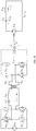
FIG. 1 is a circuit diagram of a resonant converter according to an embodiment of the present disclosure; -
FIG. 2 is a signal timing diagram of the resonant converter as shown inFIG. 1 ; -
FIG. 3a is a circuit diagram of the resonant converter as shown inFIG. 1 in an operating mode corresponding to a time period [T0-T1]; -
FIG. 3b is a circuit diagram of the resonant converter as shown inFIG. 1 in an operating mode corresponding to a time period [T1-T2]; -
FIG. 3c is a circuit diagram of the resonant converter as shown inFIG. 1 in an operating mode corresponding to a time period [T2-T3]; -
FIG. 3d is circuit diagram of the resonant converter as shown inFIG. 1 in an operating mode corresponding to a time period [T3-T4]; -
FIG. 4 is a circuit diagram of a resonant converter according to another embodiment of the present disclosure; -
FIG. 5 is a signal timing diagram of the resonant converter as shown inFIG. 4 ; and -
FIG. 6 is a circuit diagram of a resonant converter according to another embodiment of the present disclosure. - In order to make objectives, technical solutions, and advantages of embodiments of the present disclosure clearer, the technical solutions in the embodiments of the present disclosure will be described hereunder clearly and completely with reference to the accompanying drawings in the embodiments of the present disclosure. Obviously, the described embodiments are only a part of embodiments of the present disclosure, rather than all embodiments of the present disclosure. All other embodiments obtained by persons of ordinary skill in the art based on the embodiments of the present disclosure without any creative effort shall fall into the protection scope of the present disclosure.
-
FIG. 1 is a circuit diagram of a resonant converter according to an embodiment of the present disclosure. As shown inFIG. 1 , the resonant converter provided in this embodiment is adapted to provide an output voltage to a load, where the resonant converter includes: aprimary side circuit 110, aresonant network 120, atransformer 130, asecondary side circuit 140, and acontrol block 150. - Specifically, the
primary side circuit 110 described above includes at least one set of primary side switches, where theprimary side circuit 110 is configured to receive an input voltage VIN. - The
primary side circuit 110 may be a full bridge circuit or a half bridge circuit. It should be noted that, in this embodiment, the primary side circuit is not specifically limited in terms of its form, as long as the DC input voltage can be converted into a square wave voltage by the primary side circuit. For a practical application of the resonant converter provided in this embodiment, the form of the primary side circuit may be selected according to actual working conditions and design requirements, but is included in the protected scope of this embodiment. - For the
resonant network 120, it is coupled to theprimary side circuit 110 described above. Theresonant network 120 includes at least one resonant capacitor CR and at least one resonant inductor LR. For theresonant network 120 including the capacitor, the inductor and a resistor element, it may present capacitive, inductive, or resistive characteristics when working at different frequency. When resonance happens resonates, the current and voltage of theresonant network 120 periodically cross zero point, so that a switch device can be turned on or turned off under zero voltage or zero current conditions, thereby realizing soft switching and reducing switching loss. Theresonant network 120 may be a series resonant network or a parallel resonant network. It should be noted that, in this embodiment, the resonant network is not specifically limited in terms of its form. - In addition, the
transformer 130 described above has a primary side winding N1 and a secondary side winding N2, where the primary side winding N1 of thetransformer 130 is coupled to theresonant network 120 described above, and the secondary side winding N2 of thetransformer 130 is coupled to thesecondary side circuit 140. The secondary side circuit includes at least one set of secondary side switches. - The
control block 150 may control the secondary side switches according to the input voltage and the output voltage, so that the secondary side winding of the transformer is short-circuited during a preset time interval before operating state of the primary side switches changes. Further, thecontrol block 150 may also control the secondary side switches according to a current detection signal, so that the secondary side winding of the transformer is short-circuited during a preset time interval before operating state of the primary side switches changes. The current detection signal represents a current flowing through the primary side winding of thetransformer 130. Further, the corresponding preset time interval may be adjusted according to the load current. In addition, the corresponding preset time interval may also be adjusted according to the input voltage, or the like, which, notably, is not specifically limited by the present disclosure. - In an illustrative embodiment, the secondary side circuit described above may be a full bridge rectifying circuit. Specifically, the full bridge rectifying circuit includes:
- a first bridge arm including a first switch Ssi and a second switch SS2 connected in series, where a connecting node between the first switch SS1 and the second switch SS2 is electrically coupled to one end of the secondary side winding N2;
- a second bridge arm connected in parallel with the first bridge arm, where the second bridge arm includes a third switch SS3 and a fourth switch SS4 connected in series, and a connecting node between the third switch SS3 and the fourth switch SS4 is electrically coupled to the other end of the secondary side winding N2.
- During a first time period, that is, the first half switching period, the control block 150 controls the first switch SS1 and the fourth switch SS4, so that the secondary side winding N2 is short-circuited during the preset time interval (i.e. Lead Time) before operating state of the primary side switches changes;
- During a second time period, that is, the second half switching period, the control block 150 controls the second switch SS2 and the third switch SS3, so that the secondary side winding N2 is short-circuited during the preset time interval (Lead Time) before operating state of the primary side switches changes.
- In this embodiment, the control block controls the secondary side switches according to the input voltage, the output voltage and the current detection signal, so that the secondary side winding of the
transformer 130 is short-circuited during a preset time interval before operating state of the primary side switches changes. In this way, the voltage applied to theresonant network 120 is higher, thus the energy stored in theresonant network 120 is larger, which will increase the primary current to ensure ZVS of primary side switches in light-load condition. Meanwhile, the switching frequency is reduced, and the light-load efficiency may be significantly improved. It is to be understood that the light-load condition herein may refer to a condition in which the resonant converter has a load ratio of no more than 30% (e.g., 20%, 10% or 5%). - The operating mode of the resonant converter as shown in
FIG.1 will be specifically described hereunder in conjunction with a specific signal timing diagram of the resonant converter as shown inFIG. 2 ; furthermore,FIG. 3a is a circuit diagram of the resonant converter as shown inFIG. 1 in an operating mode corresponding to a time period [T0-T1];FIG. 3b is a circuit diagram of the resonant converter as shown inFIG. 1 in an operating mode corresponding to a time period [T1-T2];FIG. 3c is a circuit diagram of the resonant converter as shown inFIG. 1 in an operating mode corresponding to a time period [T2-T3]; andFIG. 3d is a circuit diagram of the resonant converter as shown inFIG. 1 in an operating mode corresponding to a time period [T3-T4]. - Reference may be made to
FIG. 2 andFIG. 3a , during the time period [T0-T1], the second switch SS2 and the third switch SS3 in the secondary side circuit are simultaneously turned on, so that thetransformer 130 is short-circuited, the input voltage VIN is then directly applied to theresonant network 120, when no energy is transferred from theresonant network 120 to the secondary side circuit. - Reference may be made to
FIG. 2 andFIG. 3b , during the time period [T1-T2], the first switch Ssi and the third switch SS3 in the switches are simultaneously turned on, the voltage difference VIN-nVO is applied to theresonant network 120, when the energy is transferred from the resonant network to the secondary side circuit and output, as shown inFIG. 3b . It can be seen that the operating mode is consistent with the conventional operating mode of the resonant converter. - Reference may be made to
FIG. 2 andFIG. 3c , the time period [T2-T3] before operating state of the primary side switches SP1, SP2, SP3 and SP4 are switched is the preset time interval TL. At the time T2, switching states of the secondary side switches SS3 and SS4 are changed so that the first switch Ssi and the fourth switch SS4 in the switches are simultaneously turned on to make the secondary side winding of thetransformer 130 short-circuited, the input voltage VIN is then directly applied to the resonant inductor LR and the resonant capacitor CR, where the current flowing through theprimary side circuit 110 increases and contributes to realizing ZVS for the primary side switches. During time period [T2-T3], the circuit diagram of the resonant converter provided in this embodiment is shown inFIG. 3c . - Reference may be made to
FIG. 2 andFIG. 3d , at the time T3, switching states of the primary side switches SP1, SP2, SP3 and SP4 are changed, the primary side switches SP1 and SP3 are turned off, and the primary side switches SP2 and SP4 are turned on. During the time period [T3-T4], the first switch Ssi and the fourth switch SS4 in the secondary side circuit are simultaneously turned on, the corresponding circuit diagram of the resonant converter provided in this embodiment is shown inFIG. 3d . - It can be seen from the operating states of the above resonant converter that, by adding the time period [T2-T3], a primary side current may be increased to obtain enough negative current required for ZVS of primary side switches in light-load condition. At the same time, by adding the time period [T2-T3], the entire switching period gets longer and the switching frequency reduces, thus further reducing the turn-off loss of the primary side switches. Therefore, by using the resonant converter provided in this embodiment, the efficiency of the resonant converter in light-load condition can be effectively improved.
- Similarly, during the second time period, the time period [T6-T7] before when operating state of the primary side switches SP1, SP2, SP3 and SP4 are switched is the preset time interval TL, during which the second switch SS2 and the third switch SS3 in the secondary side circuit are simultaneously turned on, and the
transformer 130 is short-circuited. The input voltage VIN is directly applied to the resonant inductor LR and the resonant capacitor CR. Meanwhile, the current flowing through the primary side circuit 110increases and contributes to realizing ZVS for the primary side switches. - In order to further illustrate the efficiency improvement in light-load condition when the resonant converter provided in this embodiment is operating with different input voltage, descriptions are made in conjunction with experimental data of the resonant converter provided in this embodiment and the resonant converter in prior art operating in different conditions. When both converters are in light-load condition, with an input voltage of 240V applied to the resonant converter provided in this embodiment and the resonant converter in the prior art respectively, the resonant converter provided in this embodiment has a conversion efficiency of 95%, while the resonant converter in the prior art has a conversion efficiency of only 88%; with an input voltage of 300Vapplied to the resonant converter provided in this embodiment and the resonant converter in the prior art respectively, the resonant converter provided in this embodiment has a conversion efficiency of 96.3%, while the resonant converter in the prior art has a conversion efficiency of only 88%; with an input voltage of 360V applied to the resonant converter provided in this embodiment and the resonant converter in the prior art respectively, the resonant converter provided in this embodiment has a conversion efficiency of 96.4%, while the resonant converter in the prior art has a conversion efficiency of only 89%. It can be seen that, for different input voltages, the conversion efficiency of the resonant converter provided in this embodiment is significantly higher than that of the resonant converter in the prior art in light-load condition. The respective conversion efficiencies of the resonant converter provided in this embodiment and the resonant converter in the prior art are as follows:
Input voltage Conversion efficiency of the resonant converter in the prior art Conversion efficiency of the resonant converter provided in this embodiment 240V 88% 95% 300V 88% 96.3% 360V 89% 96.4% - In some embodiments, a filter capacitor Co may be coupled to the
secondary side circuit 140 to filter the output voltage, so that the output voltage of thesecondary side circuit 140 is substantially stable. - In addition, the
control block 150 in the foregoing embodiments may be constructed with an analog circuit or a digital processor. It should be noted that, in this embodiment, the control block is not specifically limited in terms of its form, only if effective control can be achieved for the primary side switches and the secondary side switches. Reference may be made toFIG. 1 again, in a possible implementation, the control block 150 described above may include: a primary side driver and a secondary side driver, where the primary side driver controls the primary side switches SP1-SP4 according to the output voltage, and the secondary side driver controls the secondary side switches SS1- SS4 according to the input voltage, the output voltage, and the current detection signal. The control block 150 samples the input voltage and the output voltage to obtain an input voltage sample value Vin(scld) and an output voltage sample value Vo(scld), respectively. The output voltage sample value Vo(scld) is compared with a voltage reference value Vo(ref) to obtain a difference value VE, which is then calculated by error amplification and compensation circuit to obtain an output value VEA. The output value VEA is then sent to a voltage controlled oscillator, and primary side driving signals, i.e., a switching frequency fs, are then generated. On the other hand, a delay time and lead time control circuit in thecontrol block 150 determines a delay time according to a ratio between the input voltage sample value and the output voltage sample value, where the delay time starts from a zero-crossing point of a resonant current iLR (obtained by a zero-crossing detection circuit); further, the delay time and lead time control circuit determines the preset time interval(that is, the lead time) according to the load current and the switching frequency fs obtained with a closed-loop control described above, thus may generate the secondary side driving signals. -
FIG. 4 is a circuit diagram of a resonant converter according to another embodiment of the present disclosure; andFIG. 5 is a signal timing diagram of the resonant converter as shown inFIG. 4 . As shown inFIG. 4 , with reference toFIG. 1 , a resonant converter provided in this embodiment is adapted to provide an output voltage to a load, where the resonant converter includes: a primary side circuit, a resonant network, a transformer, a secondary side circuit, and a control block. - In a possible implementation, the primary side circuit described above may be a half bridge circuit. For the resonant network, it is coupled to the primary side circuit described above, and the resonant network includes at least one resonant inductor and at least one resonant capacitor, where a capacitor of the half bridge circuit itself may serve as the resonant capacitor. In addition, the transformer described above has a primary side winding N1 and a secondary side winding N2, where the primary side winding N1 of the transformer is coupled to the resonant network described above, and the secondary side winding N2 of the transformer is coupled to the secondary side circuit. The secondary side circuit includes at least one set of secondary side switches. The control block may control the secondary side switches according to the input voltage and the output voltage, so that the secondary side winding of the transformer is short-circuited during a preset time interval before operating state of the primary side switches changes. Further, the control block may also receive a current detection signal, and control the secondary side switches according to the current detection signal, so that the secondary side winding of the transformer is short-circuited during a preset time interval before operating state of the primary side switches changes. The current detection signal represents a current flowing through the primary side winding of the transformer. Moreover, the corresponding preset time interval may be adjusted according to the load current, the input voltage, or the like, and which is not limited in the disclosure.
- Descriptions will be made hereunder in detail to operating modes of the resonant converter in conjunction with
FIG. 5 . During the time period [T0-T1], the second switch SS2 and the third switch SS3 in the secondary side circuit are simultaneously turned on, so that the transformer is short-circuited, the input voltage Vin is then directly applied to the resonant network, when no energy is transferred from the resonant network to the secondary side circuit and output; during the time period [T1-T2], the first switch SS1 and the third switch SS3 in the secondary side circuit are simultaneously turned on, the voltage difference Vin-nVo is applied to the resonant network, when the energy is transferred from the resonant network to the output; at the time T2, switching states of the third switch SS3 and the fourth switch SS4 are changed. The time period [T2-T3] is the preset time interval TL, during which the first switch SS1 and the fourth switch SS4 in the secondary side circuit are simultaneously turned on to make the secondary side winding of the transformer short-circuited, the input voltage VIN is then directly applied to the resonant network where the current flowing through the primary side circuit increases and contributes to realizing ZVS for the primary side switches; at the time T3, states of the primary side switches SP1, SP2, SP3 and SP4 in the primary side circuit are switched. During the time period [T3-T4], the first switch Ssi and the fourth switch SS4 in the secondary side circuit are simultaneously turned on. Similarly, in the second half switch cycle, [T6-T7] is the preset time interval TL, and the second switch SS2 and the third switch SS3 are simultaneously turned on, so that the transformer is short-circuited. The input voltage Vin is directly applied to the resonant network. At this time, the current of the primary side circuit increases, which is advantageous for the primary side switches to realize ZVS. - It can be seen from the operating states of the above resonant converter that, by adding the time period [T2-T3] and [T6-T7], a primary side current may be increased to obtain enough negative current required for ZVS of primary side switches in light-load condition. At the same time, by adding the time period [T2-T3] and [T6-T7], the entire switching period gets longer and the switching frequency reduces, thus further reducing the turn-off loss of the primary side switches. Therefore, by using the resonant converter provided in this embodiment, the efficiency of the resonant converter in light-load condition may be effectively improved.
-
FIG. 6 is a circuit diagram of a resonant converter according to another embodiment of the present disclosure. As shown inFIG. 6 , with reference toFIG. 1 , a resonant converter provided in this embodiment is adapted to provide an output voltage to a load, where the resonant converter includes: a primary side circuit, a resonant network, a transformer, a secondary side circuit, and a control block. - In a possible implementation, the secondary side circuit described above may be a center-tap rectifying circuit that includes: a first switch SS1 and a second switch SS2 electrically coupled to the secondary side winding respectively.
- Finally, it should be noted that the foregoing embodiments are merely intended for describing the technical solutions of the present disclosure rather than limiting the present disclosure. Although the present disclosure is described in detail with reference to the foregoing embodiments, persons of ordinary skill in the art should understand that they may still make modifications to the technical solutions described in the foregoing embodiments, or make equivalent replacements to some or all technical features therein; however, these modifications or replacements do not make the essence of corresponding technical solutions depart from the scope of the technical solutions in the embodiments of the present disclosure.
Claims (15)
- A resonant converter adapted to provide an output voltage to a load, comprising:a primary side circuit (110) comprising at least one set of primary side switches, wherein the primary side circuit (110) is configured to receive an input voltage;a resonant network (120) coupled to the primary side circuit (110);a transformer (130) having a primary side winding and a secondary side winding, wherein the primary side winding is coupled to the resonant network (120);a secondary side circuit (140) comprising at least one set of secondary side switches, wherein the secondary side circuit (140) is coupled to the secondary side winding of the transformer (130); anda control block (150) that controls the secondary side switches according to the input voltage and the output voltage, wherein the secondary side winding of the transformer (130) is short-circuited during a preset time interval before operating state of the primary side switches changes.
- The resonant converter according to claim 1, wherein the secondary side circuit (140) is a full-bridge rectifying circuit or a center-tap rectifying circuit.
- The resonant converter according to claim 2, wherein the secondary side circuit (140) is a full-bridge rectifying circuit that comprises:a first bridge arm comprising a first switch and a second switch connected in series, wherein a common node between the first switch and the second switch is electrically coupled to one end of the secondary side winding; anda second bridge arm connected in parallel with the first bridge arm, wherein the second bridge arm comprises a third switch and a fourth switch connected in series, and a common node between the third switch and the fourth switch is electrically coupled to the other end of the secondary side winding;wherein during a first time period, the control block (150) controls, during the preset time interval before operating state of the primary side switches changes, the first switch and the fourth switch to be simultaneously turned on; andduring a second time period, the control block (150) controls, during the preset time interval before operating state of the primary side switches changes, the second switch and the third switch to be simultaneously turned on.
- The resonant converter according to claim 3, wherein the control block (150) further controls, during the preset time interval of the first time period, the second switch and the third switch to be simultaneously turned off; the control block (150) further controls, during the preset time interval of the second time period, the first switch and the fourth switch to be simultaneously turned off.
- The resonant converter according to any one of claims 1 to 4, wherein the resonant converter further comprises a filter capacitor coupled to the secondary side circuit (140).
- The resonant converter according to any one of claims 1 to 5, wherein the primary side circuit (110) is a full bridge circuit or a half bridge circuit.
- The resonant converter according to any one of claims 1 to 6, wherein the control block (150) comprises: a primary side driver and a secondary side driver,
wherein the primary side driver controls the primary side switches according to the output voltage and the secondary side driver controls the secondary side switches according to the input voltage and the output voltage. - The resonant converter according to any one of claims 1 to 7, wherein the resonant converter operates in light-load condition.
- A control method of a resonant converter, wherein the resonant converter comprises a primary side circuit (110), a resonant network (120), a transformer (130) having a primary side winding and a secondary side winding, and a secondary side circuit (140), the resonant network (120) is electrically coupled to the primary side circuit (110) and the primary side winding of the transformer (130), and the secondary side circuit (140) is electrically coupled to the secondary side winding of the transformer (130), the primary side circuit (110) includes at least one set of primary side switches, and the secondary side circuit (140) includes at least one set of secondary side switches, the method comprising:detecting an input voltage received by the primary side circuit (110);detecting an output voltage generated by the secondary side circuit (140);controlling the at least one set of secondary side switches of the secondary side circuit (140) according to the input voltage and the output voltage, wherein the secondary side winding of the transformer (130) is short-circuited during a preset time interval before operating state of the at least one set of primary side switches changes.
- The control method according to claim 9, further comprising:obtaining a current detection signal; andcontrolling the secondary side switches according to the input voltage, the output voltage and the current detection signal.
- The control method according to claim 10, wherein the current detection signal reflects a current flowing through the primary side winding.
- The control method according to any one of claims 9 to 11, wherein the control method is applied to the resonant converter operating in light-load condition.
- The control method according to claim 12, wherein the control method controls the at least one set of primary side switches to be each turned on at zero voltage.
- The control method according to any one of claims 9 to 11, wherein the preset time interval is adjusted according to a load current or the input voltage.
- The control method according to any one of claims 9 to 11, wherein the secondary side circuit (140) is a full-bridge rectifying circuit or a center-tap rectifying circuit.
Applications Claiming Priority (1)
| Application Number | Priority Date | Filing Date | Title |
|---|---|---|---|
| CN201810638360.2A CN110620512B (en) | 2018-06-20 | 2018-06-20 | Resonant converter and control method |
Publications (2)
| Publication Number | Publication Date |
|---|---|
| EP3584919A1 true EP3584919A1 (en) | 2019-12-25 |
| EP3584919B1 EP3584919B1 (en) | 2022-03-16 |
Family
ID=66999639
Family Applications (1)
| Application Number | Title | Priority Date | Filing Date |
|---|---|---|---|
| EP19181320.3A Active EP3584919B1 (en) | 2018-06-20 | 2019-06-19 | Resonant converter and control method |
Country Status (3)
| Country | Link |
|---|---|
| US (2) | US10756617B2 (en) |
| EP (1) | EP3584919B1 (en) |
| CN (1) | CN110620512B (en) |
Families Citing this family (12)
| Publication number | Priority date | Publication date | Assignee | Title |
|---|---|---|---|---|
| IT201900006719A1 (en) * | 2019-05-10 | 2020-11-10 | St Microelectronics Srl | ELECTRONIC CONVERTER |
| JP7472654B2 (en) * | 2020-05-27 | 2024-04-23 | 富士電機株式会社 | Switching control circuit, LLC converter |
| US11594976B2 (en) * | 2020-06-05 | 2023-02-28 | Delta Electronics, Inc. | Power converter and control method thereof |
| US11594973B2 (en) * | 2020-08-04 | 2023-02-28 | Delta Electronics Inc. | Multiple-port bidirectional converter and control method thereof |
| CN112072922B (en) * | 2020-09-01 | 2022-11-25 | 亚瑞源科技(深圳)有限公司 | Conversion device with shock absorption control and operation method of shock absorption control thereof |
| CN115776234A (en) * | 2021-09-08 | 2023-03-10 | 台达电子企业管理(上海)有限公司 | Resonant converter and method of operating the same |
| CN115800747A (en) * | 2021-09-10 | 2023-03-14 | 台达电子企业管理(上海)有限公司 | Hybrid flyback circuit and control method |
| CN114006536B (en) * | 2021-10-25 | 2024-04-16 | 联合汽车电子有限公司 | Double active bridge series resonant converter and control method thereof |
| TWI780983B (en) * | 2021-11-12 | 2022-10-11 | 國立臺灣科技大學 | Resonant converter using pre-conduction mechanism to realize wide output voltage range |
| CN114157156A (en) * | 2021-12-02 | 2022-03-08 | 台达电子企业管理(上海)有限公司 | Three-level rectification DC/DC converter |
| CN117439413A (en) * | 2022-07-15 | 2024-01-23 | 台达电子企业管理(上海)有限公司 | Resonant converter, control method and modulation method thereof |
| CN117240105B (en) * | 2023-11-16 | 2024-03-01 | 杭州蔚斯博系统科技有限公司 | Bridge resonant converter control method and bridge resonant converter |
Citations (1)
| Publication number | Priority date | Publication date | Assignee | Title |
|---|---|---|---|---|
| US20160294294A1 (en) * | 2015-04-01 | 2016-10-06 | Futurewei Technologies, Inc. | Resonant Converters with an Improved Voltage Regulation Range |
Family Cites Families (21)
| Publication number | Priority date | Publication date | Assignee | Title |
|---|---|---|---|---|
| JP2004215469A (en) * | 2003-01-09 | 2004-07-29 | Renesas Technology Corp | Switching power supply and semiconductor integrated circuit for controlling power supply |
| DE102005047551A1 (en) * | 2005-09-30 | 2007-04-12 | Siemens Ag | Exciter device for an electrical machine |
| FR2900513B1 (en) * | 2006-04-26 | 2010-05-21 | Thales Sa | PERFECTED ISOLATED POWER TRANSFER DEVICE |
| US7796406B2 (en) * | 2007-07-31 | 2010-09-14 | Lumenis Ltd. | Apparatus and method for high efficiency isolated power converter |
| JP4790826B2 (en) * | 2009-03-10 | 2011-10-12 | 株式会社日立製作所 | Power supply device and hard disk device |
| US8717783B2 (en) * | 2009-10-30 | 2014-05-06 | Delta Electronics (Shanghai) Co., Ltd. | Method and apparatus for regulating gain within a resonant converter |
| JP5530212B2 (en) * | 2010-02-10 | 2014-06-25 | 株式会社日立製作所 | Power supply device, hard disk device, and switching method of power supply device |
| US8811039B2 (en) * | 2010-07-16 | 2014-08-19 | Virginia Tech Intellectual Properties, Inc. | Pulse width modulated resonant power conversion |
| CN102291002B (en) | 2011-08-09 | 2014-11-12 | 联合汽车电子有限公司 | Control method of phase-shifted full-bridge circuit |
| US9178438B2 (en) * | 2012-04-05 | 2015-11-03 | Futurewei Technologies, Inc. | Apparatus for resonant converters |
| US9356523B2 (en) * | 2012-12-28 | 2016-05-31 | Panasonic Intellectual Property Management Co., Ltd. | DC-to-DC converter |
| JP2014217196A (en) * | 2013-04-26 | 2014-11-17 | パナソニック株式会社 | Bidirectional dc/dc converter |
| AT515242B1 (en) * | 2013-12-20 | 2020-04-15 | Fronius Int Gmbh | Method of controlling a full bridge DC / DC converter |
| US9490704B2 (en) * | 2014-02-12 | 2016-11-08 | Delta Electronics, Inc. | System and methods for controlling secondary side switches in resonant power converters |
| US9985516B2 (en) * | 2014-02-12 | 2018-05-29 | Palo Alto Research Center Incorporated | DC/DC converter and method for zero voltage switching |
| JP6241334B2 (en) * | 2014-03-14 | 2017-12-06 | Tdk株式会社 | Current resonance type DCDC converter |
| US9461554B2 (en) * | 2014-09-30 | 2016-10-04 | Futurewei Technologies, Inc. | Hybrid converter using a resonant stage and a non-isolated stage |
| US9762135B2 (en) * | 2014-11-05 | 2017-09-12 | Infineon Technologies Austria Ag | Secondary side control of resonant DC/DC converters |
| CN107294413B (en) * | 2016-04-08 | 2021-01-05 | 松下知识产权经营株式会社 | Power conversion device |
| JP6848255B2 (en) * | 2016-08-10 | 2021-03-24 | Tdk株式会社 | Switching power supply |
| CN106505869A (en) * | 2016-11-01 | 2017-03-15 | 东南大学 | A kind of grid-connected combined type resonant full bridge changer of new forms of energy direct current and control method |
-
2018
- 2018-06-20 CN CN201810638360.2A patent/CN110620512B/en active Active
-
2019
- 2019-02-27 US US16/286,619 patent/US10756617B2/en active Active
- 2019-06-19 EP EP19181320.3A patent/EP3584919B1/en active Active
-
2020
- 2020-07-17 US US16/931,460 patent/US11075575B2/en active Active
Patent Citations (1)
| Publication number | Priority date | Publication date | Assignee | Title |
|---|---|---|---|---|
| US20160294294A1 (en) * | 2015-04-01 | 2016-10-06 | Futurewei Technologies, Inc. | Resonant Converters with an Improved Voltage Regulation Range |
Also Published As
| Publication number | Publication date |
|---|---|
| CN110620512B (en) | 2020-09-15 |
| US10756617B2 (en) | 2020-08-25 |
| US11075575B2 (en) | 2021-07-27 |
| US20200350815A1 (en) | 2020-11-05 |
| CN110620512A (en) | 2019-12-27 |
| EP3584919B1 (en) | 2022-03-16 |
| US20190393769A1 (en) | 2019-12-26 |
Similar Documents
| Publication | Publication Date | Title |
|---|---|---|
| US11075575B2 (en) | Resonant converter and control method of the resonant converter | |
| TWI750780B (en) | Isolated dc/dc converters for wide output voltage range and control methods thereof | |
| US5132889A (en) | Resonant-transition DC-to-DC converter | |
| US6452814B1 (en) | Zero voltage switching cells for power converters | |
| US8542501B2 (en) | Switching power-supply apparatus | |
| KR101840315B1 (en) | Method for controlling a series resonant dc/dc converter | |
| KR101923317B1 (en) | Bidirectional full-bridge converter and control method thereof | |
| JPH10337021A (en) | Phase crossing full bridge converter accompanied with soft pwm switching | |
| EP3633840A1 (en) | Converter | |
| KR20150044317A (en) | Converter and driving method thereof | |
| CN113632354B (en) | Soft Start of Resonant Converter | |
| KR20200056275A (en) | A two-stage power conversion converter | |
| CN114884355A (en) | Power conversion module | |
| CN112087140B (en) | Multi-mode automatic switching two-stage resonance DC-DC converter | |
| JP2002233150A (en) | Resonance-type dc-to-dc converter | |
| JP2002191174A (en) | Power supply | |
| JP2002315331A (en) | Power supply equipped with dc-dc converter | |
| JP6964565B2 (en) | Power converter and its control method | |
| JPH05176532A (en) | Power circuit | |
| US11870332B2 (en) | Power conversion circuit with transformer | |
| JP2004040854A (en) | Switching power source | |
| KR102306880B1 (en) | High efficiency isolated pfc converter | |
| US10075055B2 (en) | Zero-voltage-switching scheme for phase shift converters | |
| JPH08340676A (en) | Control method and controller for resonant power converter | |
| CN109194168B (en) | Efficient rectifying circuit and control method thereof |
Legal Events
| Date | Code | Title | Description |
|---|---|---|---|
| PUAI | Public reference made under article 153(3) epc to a published international application that has entered the european phase |
Free format text: ORIGINAL CODE: 0009012 |
|
| STAA | Information on the status of an ep patent application or granted ep patent |
Free format text: STATUS: THE APPLICATION HAS BEEN PUBLISHED |
|
| AK | Designated contracting states |
Kind code of ref document: A1 Designated state(s): AL AT BE BG CH CY CZ DE DK EE ES FI FR GB GR HR HU IE IS IT LI LT LU LV MC MK MT NL NO PL PT RO RS SE SI SK SM TR |
|
| AX | Request for extension of the european patent |
Extension state: BA ME |
|
| STAA | Information on the status of an ep patent application or granted ep patent |
Free format text: STATUS: REQUEST FOR EXAMINATION WAS MADE |
|
| 17P | Request for examination filed |
Effective date: 20200616 |
|
| RBV | Designated contracting states (corrected) |
Designated state(s): AL AT BE BG CH CY CZ DE DK EE ES FI FR GB GR HR HU IE IS IT LI LT LU LV MC MK MT NL NO PL PT RO RS SE SI SK SM TR |
|
| STAA | Information on the status of an ep patent application or granted ep patent |
Free format text: STATUS: EXAMINATION IS IN PROGRESS |
|
| 17Q | First examination report despatched |
Effective date: 20201009 |
|
| STAA | Information on the status of an ep patent application or granted ep patent |
Free format text: STATUS: EXAMINATION IS IN PROGRESS |
|
| GRAP | Despatch of communication of intention to grant a patent |
Free format text: ORIGINAL CODE: EPIDOSNIGR1 |
|
| STAA | Information on the status of an ep patent application or granted ep patent |
Free format text: STATUS: GRANT OF PATENT IS INTENDED |
|
| RIC1 | Information provided on ipc code assigned before grant |
Ipc: H02M 3/00 20060101ALN20211016BHEP Ipc: H02M 1/00 20060101ALN20211016BHEP Ipc: H02M 3/335 20060101AFI20211016BHEP |
|
| INTG | Intention to grant announced |
Effective date: 20211103 |
|
| GRAS | Grant fee paid |
Free format text: ORIGINAL CODE: EPIDOSNIGR3 |
|
| GRAA | (expected) grant |
Free format text: ORIGINAL CODE: 0009210 |
|
| STAA | Information on the status of an ep patent application or granted ep patent |
Free format text: STATUS: THE PATENT HAS BEEN GRANTED |
|
| AK | Designated contracting states |
Kind code of ref document: B1 Designated state(s): AL AT BE BG CH CY CZ DE DK EE ES FI FR GB GR HR HU IE IS IT LI LT LU LV MC MK MT NL NO PL PT RO RS SE SI SK SM TR |
|
| REG | Reference to a national code |
Ref country code: GB Ref legal event code: FG4D |
|
| REG | Reference to a national code |
Ref country code: CH Ref legal event code: EP Ref country code: DE Ref legal event code: R096 Ref document number: 602019012519 Country of ref document: DE |
|
| REG | Reference to a national code |
Ref country code: IE Ref legal event code: FG4D Ref country code: NL Ref legal event code: FP |
|
| REG | Reference to a national code |
Ref country code: AT Ref legal event code: REF Ref document number: 1476589 Country of ref document: AT Kind code of ref document: T Effective date: 20220415 |
|
| REG | Reference to a national code |
Ref country code: LT Ref legal event code: MG9D |
|
| PG25 | Lapsed in a contracting state [announced via postgrant information from national office to epo] |
Ref country code: SE Free format text: LAPSE BECAUSE OF FAILURE TO SUBMIT A TRANSLATION OF THE DESCRIPTION OR TO PAY THE FEE WITHIN THE PRESCRIBED TIME-LIMIT Effective date: 20220316 Ref country code: RS Free format text: LAPSE BECAUSE OF FAILURE TO SUBMIT A TRANSLATION OF THE DESCRIPTION OR TO PAY THE FEE WITHIN THE PRESCRIBED TIME-LIMIT Effective date: 20220316 Ref country code: NO Free format text: LAPSE BECAUSE OF FAILURE TO SUBMIT A TRANSLATION OF THE DESCRIPTION OR TO PAY THE FEE WITHIN THE PRESCRIBED TIME-LIMIT Effective date: 20220616 Ref country code: LT Free format text: LAPSE BECAUSE OF FAILURE TO SUBMIT A TRANSLATION OF THE DESCRIPTION OR TO PAY THE FEE WITHIN THE PRESCRIBED TIME-LIMIT Effective date: 20220316 Ref country code: HR Free format text: LAPSE BECAUSE OF FAILURE TO SUBMIT A TRANSLATION OF THE DESCRIPTION OR TO PAY THE FEE WITHIN THE PRESCRIBED TIME-LIMIT Effective date: 20220316 Ref country code: BG Free format text: LAPSE BECAUSE OF FAILURE TO SUBMIT A TRANSLATION OF THE DESCRIPTION OR TO PAY THE FEE WITHIN THE PRESCRIBED TIME-LIMIT Effective date: 20220616 |
|
| REG | Reference to a national code |
Ref country code: AT Ref legal event code: MK05 Ref document number: 1476589 Country of ref document: AT Kind code of ref document: T Effective date: 20220316 |
|
| PG25 | Lapsed in a contracting state [announced via postgrant information from national office to epo] |
Ref country code: LV Free format text: LAPSE BECAUSE OF FAILURE TO SUBMIT A TRANSLATION OF THE DESCRIPTION OR TO PAY THE FEE WITHIN THE PRESCRIBED TIME-LIMIT Effective date: 20220316 Ref country code: GR Free format text: LAPSE BECAUSE OF FAILURE TO SUBMIT A TRANSLATION OF THE DESCRIPTION OR TO PAY THE FEE WITHIN THE PRESCRIBED TIME-LIMIT Effective date: 20220617 Ref country code: FI Free format text: LAPSE BECAUSE OF FAILURE TO SUBMIT A TRANSLATION OF THE DESCRIPTION OR TO PAY THE FEE WITHIN THE PRESCRIBED TIME-LIMIT Effective date: 20220316 |
|
| PG25 | Lapsed in a contracting state [announced via postgrant information from national office to epo] |
Ref country code: SM Free format text: LAPSE BECAUSE OF FAILURE TO SUBMIT A TRANSLATION OF THE DESCRIPTION OR TO PAY THE FEE WITHIN THE PRESCRIBED TIME-LIMIT Effective date: 20220316 Ref country code: SK Free format text: LAPSE BECAUSE OF FAILURE TO SUBMIT A TRANSLATION OF THE DESCRIPTION OR TO PAY THE FEE WITHIN THE PRESCRIBED TIME-LIMIT Effective date: 20220316 Ref country code: RO Free format text: LAPSE BECAUSE OF FAILURE TO SUBMIT A TRANSLATION OF THE DESCRIPTION OR TO PAY THE FEE WITHIN THE PRESCRIBED TIME-LIMIT Effective date: 20220316 Ref country code: PT Free format text: LAPSE BECAUSE OF FAILURE TO SUBMIT A TRANSLATION OF THE DESCRIPTION OR TO PAY THE FEE WITHIN THE PRESCRIBED TIME-LIMIT Effective date: 20220718 Ref country code: ES Free format text: LAPSE BECAUSE OF FAILURE TO SUBMIT A TRANSLATION OF THE DESCRIPTION OR TO PAY THE FEE WITHIN THE PRESCRIBED TIME-LIMIT Effective date: 20220316 Ref country code: EE Free format text: LAPSE BECAUSE OF FAILURE TO SUBMIT A TRANSLATION OF THE DESCRIPTION OR TO PAY THE FEE WITHIN THE PRESCRIBED TIME-LIMIT Effective date: 20220316 Ref country code: CZ Free format text: LAPSE BECAUSE OF FAILURE TO SUBMIT A TRANSLATION OF THE DESCRIPTION OR TO PAY THE FEE WITHIN THE PRESCRIBED TIME-LIMIT Effective date: 20220316 Ref country code: AT Free format text: LAPSE BECAUSE OF FAILURE TO SUBMIT A TRANSLATION OF THE DESCRIPTION OR TO PAY THE FEE WITHIN THE PRESCRIBED TIME-LIMIT Effective date: 20220316 |
|
| PG25 | Lapsed in a contracting state [announced via postgrant information from national office to epo] |
Ref country code: PL Free format text: LAPSE BECAUSE OF FAILURE TO SUBMIT A TRANSLATION OF THE DESCRIPTION OR TO PAY THE FEE WITHIN THE PRESCRIBED TIME-LIMIT Effective date: 20220316 Ref country code: IS Free format text: LAPSE BECAUSE OF FAILURE TO SUBMIT A TRANSLATION OF THE DESCRIPTION OR TO PAY THE FEE WITHIN THE PRESCRIBED TIME-LIMIT Effective date: 20220716 Ref country code: AL Free format text: LAPSE BECAUSE OF FAILURE TO SUBMIT A TRANSLATION OF THE DESCRIPTION OR TO PAY THE FEE WITHIN THE PRESCRIBED TIME-LIMIT Effective date: 20220316 |
|
| REG | Reference to a national code |
Ref country code: DE Ref legal event code: R097 Ref document number: 602019012519 Country of ref document: DE |
|
| PLBE | No opposition filed within time limit |
Free format text: ORIGINAL CODE: 0009261 |
|
| STAA | Information on the status of an ep patent application or granted ep patent |
Free format text: STATUS: NO OPPOSITION FILED WITHIN TIME LIMIT |
|
| PG25 | Lapsed in a contracting state [announced via postgrant information from national office to epo] |
Ref country code: MC Free format text: LAPSE BECAUSE OF FAILURE TO SUBMIT A TRANSLATION OF THE DESCRIPTION OR TO PAY THE FEE WITHIN THE PRESCRIBED TIME-LIMIT Effective date: 20220316 Ref country code: DK Free format text: LAPSE BECAUSE OF FAILURE TO SUBMIT A TRANSLATION OF THE DESCRIPTION OR TO PAY THE FEE WITHIN THE PRESCRIBED TIME-LIMIT Effective date: 20220316 |
|
| REG | Reference to a national code |
Ref country code: CH Ref legal event code: PL |
|
| REG | Reference to a national code |
Ref country code: BE Ref legal event code: MM Effective date: 20220630 |
|
| 26N | No opposition filed |
Effective date: 20221219 |
|
| PG25 | Lapsed in a contracting state [announced via postgrant information from national office to epo] |
Ref country code: SI Free format text: LAPSE BECAUSE OF FAILURE TO SUBMIT A TRANSLATION OF THE DESCRIPTION OR TO PAY THE FEE WITHIN THE PRESCRIBED TIME-LIMIT Effective date: 20220316 |
|
| PG25 | Lapsed in a contracting state [announced via postgrant information from national office to epo] |
Ref country code: LU Free format text: LAPSE BECAUSE OF NON-PAYMENT OF DUE FEES Effective date: 20220619 Ref country code: LI Free format text: LAPSE BECAUSE OF NON-PAYMENT OF DUE FEES Effective date: 20220630 Ref country code: IE Free format text: LAPSE BECAUSE OF NON-PAYMENT OF DUE FEES Effective date: 20220619 Ref country code: FR Free format text: LAPSE BECAUSE OF NON-PAYMENT OF DUE FEES Effective date: 20220630 Ref country code: CH Free format text: LAPSE BECAUSE OF NON-PAYMENT OF DUE FEES Effective date: 20220630 |
|
| PG25 | Lapsed in a contracting state [announced via postgrant information from national office to epo] |
Ref country code: BE Free format text: LAPSE BECAUSE OF NON-PAYMENT OF DUE FEES Effective date: 20220630 |
|
| PG25 | Lapsed in a contracting state [announced via postgrant information from national office to epo] |
Ref country code: IT Free format text: LAPSE BECAUSE OF FAILURE TO SUBMIT A TRANSLATION OF THE DESCRIPTION OR TO PAY THE FEE WITHIN THE PRESCRIBED TIME-LIMIT Effective date: 20220316 |
|
| PGFP | Annual fee paid to national office [announced via postgrant information from national office to epo] |
Ref country code: NL Payment date: 20230515 Year of fee payment: 5 Ref country code: DE Payment date: 20230425 Year of fee payment: 5 |
|
| GBPC | Gb: european patent ceased through non-payment of renewal fee |
Effective date: 20230619 |
|
| PG25 | Lapsed in a contracting state [announced via postgrant information from national office to epo] |
Ref country code: MK Free format text: LAPSE BECAUSE OF FAILURE TO SUBMIT A TRANSLATION OF THE DESCRIPTION OR TO PAY THE FEE WITHIN THE PRESCRIBED TIME-LIMIT Effective date: 20220316 Ref country code: CY Free format text: LAPSE BECAUSE OF FAILURE TO SUBMIT A TRANSLATION OF THE DESCRIPTION OR TO PAY THE FEE WITHIN THE PRESCRIBED TIME-LIMIT Effective date: 20220316 Ref country code: GB Free format text: LAPSE BECAUSE OF NON-PAYMENT OF DUE FEES Effective date: 20230619 |