EP3576278A1 - Frequency inverter - Google Patents
Frequency inverter Download PDFInfo
- Publication number
- EP3576278A1 EP3576278A1 EP18174782.5A EP18174782A EP3576278A1 EP 3576278 A1 EP3576278 A1 EP 3576278A1 EP 18174782 A EP18174782 A EP 18174782A EP 3576278 A1 EP3576278 A1 EP 3576278A1
- Authority
- EP
- European Patent Office
- Prior art keywords
- input
- output
- semiconductor
- frequency converter
- capacitor device
- Prior art date
- Legal status (The legal status is an assumption and is not a legal conclusion. Google has not performed a legal analysis and makes no representation as to the accuracy of the status listed.)
- Withdrawn
Links
Images


Classifications
-
- H—ELECTRICITY
- H02—GENERATION; CONVERSION OR DISTRIBUTION OF ELECTRIC POWER
- H02M—APPARATUS FOR CONVERSION BETWEEN AC AND AC, BETWEEN AC AND DC, OR BETWEEN DC AND DC, AND FOR USE WITH MAINS OR SIMILAR POWER SUPPLY SYSTEMS; CONVERSION OF DC OR AC INPUT POWER INTO SURGE OUTPUT POWER; CONTROL OR REGULATION THEREOF
- H02M5/00—Conversion of ac power input into ac power output, e.g. for change of voltage, for change of frequency, for change of number of phases
- H02M5/40—Conversion of ac power input into ac power output, e.g. for change of voltage, for change of frequency, for change of number of phases with intermediate conversion into dc
- H02M5/42—Conversion of ac power input into ac power output, e.g. for change of voltage, for change of frequency, for change of number of phases with intermediate conversion into dc by static converters
- H02M5/44—Conversion of ac power input into ac power output, e.g. for change of voltage, for change of frequency, for change of number of phases with intermediate conversion into dc by static converters using discharge tubes or semiconductor devices to convert the intermediate dc into ac
- H02M5/453—Conversion of ac power input into ac power output, e.g. for change of voltage, for change of frequency, for change of number of phases with intermediate conversion into dc by static converters using discharge tubes or semiconductor devices to convert the intermediate dc into ac using devices of a triode or transistor type requiring continuous application of a control signal
- H02M5/458—Conversion of ac power input into ac power output, e.g. for change of voltage, for change of frequency, for change of number of phases with intermediate conversion into dc by static converters using discharge tubes or semiconductor devices to convert the intermediate dc into ac using devices of a triode or transistor type requiring continuous application of a control signal using semiconductor devices only
-
- B—PERFORMING OPERATIONS; TRANSPORTING
- B60—VEHICLES IN GENERAL
- B60L—PROPULSION OF ELECTRICALLY-PROPELLED VEHICLES; SUPPLYING ELECTRIC POWER FOR AUXILIARY EQUIPMENT OF ELECTRICALLY-PROPELLED VEHICLES; ELECTRODYNAMIC BRAKE SYSTEMS FOR VEHICLES IN GENERAL; MAGNETIC SUSPENSION OR LEVITATION FOR VEHICLES; MONITORING OPERATING VARIABLES OF ELECTRICALLY-PROPELLED VEHICLES; ELECTRIC SAFETY DEVICES FOR ELECTRICALLY-PROPELLED VEHICLES
- B60L9/00—Electric propulsion with power supply external to the vehicle
- B60L9/16—Electric propulsion with power supply external to the vehicle using ac induction motors
- B60L9/24—Electric propulsion with power supply external to the vehicle using ac induction motors fed from ac supply lines
-
- H—ELECTRICITY
- H02—GENERATION; CONVERSION OR DISTRIBUTION OF ELECTRIC POWER
- H02M—APPARATUS FOR CONVERSION BETWEEN AC AND AC, BETWEEN AC AND DC, OR BETWEEN DC AND DC, AND FOR USE WITH MAINS OR SIMILAR POWER SUPPLY SYSTEMS; CONVERSION OF DC OR AC INPUT POWER INTO SURGE OUTPUT POWER; CONTROL OR REGULATION THEREOF
- H02M5/00—Conversion of ac power input into ac power output, e.g. for change of voltage, for change of frequency, for change of number of phases
- H02M5/02—Conversion of ac power input into ac power output, e.g. for change of voltage, for change of frequency, for change of number of phases without intermediate conversion into dc
- H02M5/04—Conversion of ac power input into ac power output, e.g. for change of voltage, for change of frequency, for change of number of phases without intermediate conversion into dc by static converters
- H02M5/22—Conversion of ac power input into ac power output, e.g. for change of voltage, for change of frequency, for change of number of phases without intermediate conversion into dc by static converters using discharge tubes with control electrode or semiconductor devices with control electrode
- H02M5/225—Conversion of ac power input into ac power output, e.g. for change of voltage, for change of frequency, for change of number of phases without intermediate conversion into dc by static converters using discharge tubes with control electrode or semiconductor devices with control electrode comprising two stages of AC-AC conversion, e.g. having a high frequency intermediate link
-
- H—ELECTRICITY
- H02—GENERATION; CONVERSION OR DISTRIBUTION OF ELECTRIC POWER
- H02M—APPARATUS FOR CONVERSION BETWEEN AC AND AC, BETWEEN AC AND DC, OR BETWEEN DC AND DC, AND FOR USE WITH MAINS OR SIMILAR POWER SUPPLY SYSTEMS; CONVERSION OF DC OR AC INPUT POWER INTO SURGE OUTPUT POWER; CONTROL OR REGULATION THEREOF
- H02M5/00—Conversion of ac power input into ac power output, e.g. for change of voltage, for change of frequency, for change of number of phases
- H02M5/40—Conversion of ac power input into ac power output, e.g. for change of voltage, for change of frequency, for change of number of phases with intermediate conversion into dc
- H02M5/42—Conversion of ac power input into ac power output, e.g. for change of voltage, for change of frequency, for change of number of phases with intermediate conversion into dc by static converters
- H02M5/44—Conversion of ac power input into ac power output, e.g. for change of voltage, for change of frequency, for change of number of phases with intermediate conversion into dc by static converters using discharge tubes or semiconductor devices to convert the intermediate dc into ac
- H02M5/453—Conversion of ac power input into ac power output, e.g. for change of voltage, for change of frequency, for change of number of phases with intermediate conversion into dc by static converters using discharge tubes or semiconductor devices to convert the intermediate dc into ac using devices of a triode or transistor type requiring continuous application of a control signal
- H02M5/458—Conversion of ac power input into ac power output, e.g. for change of voltage, for change of frequency, for change of number of phases with intermediate conversion into dc by static converters using discharge tubes or semiconductor devices to convert the intermediate dc into ac using devices of a triode or transistor type requiring continuous application of a control signal using semiconductor devices only
- H02M5/4585—Conversion of ac power input into ac power output, e.g. for change of voltage, for change of frequency, for change of number of phases with intermediate conversion into dc by static converters using discharge tubes or semiconductor devices to convert the intermediate dc into ac using devices of a triode or transistor type requiring continuous application of a control signal using semiconductor devices only having a rectifier with controlled elements
Definitions
- Such a frequency converter and the associated electric drive are for example from the DE 103 23 218 A1 known.
- Electric railway systems usually operate with a single-phase AC voltage, which is supplied to electrically powered rail vehicles via a running above the tracks overhead line.
- Typical are an AC voltage with a rated voltage of 15 kV and a frequency of 16 2/3 Hz or an AC voltage with a rated voltage of 25 kV and a frequency of 50 Hz.
- other voltage systems are known.
- the high alternating voltage is selected because this results in relatively low currents flowing in the overhead line and thus electrical losses can be minimized.
- Traction motors and traction converters of electric trains are not designed for such a high AC voltage, but only for much lower operating voltages.
- the AC voltage of the overhead line must therefore be reduced accordingly before the electrical energy is supplied to the traction converters and traction motors.
- the electrical equipment of the rail vehicle is also galvanically separated from the overhead line at the same time. As a result, an insulation fault, for example, of a traction motor with respect to the ground potential does not lead to a short-circuit current, but only to initiate insulation monitoring.
- the AC voltage of the catenary is lowered by means of a transformer to the input voltage of the traction converter.
- the transformer also provides the galvanic isolation between the drive on the one hand and the AC voltage realized on the other hand.
- Such systems require - apart from suitable shutdown, filtering, measuring and protection devices on the primary side of the transformer - no other facilities.
- the conventional prior art transformer must be designed for the operating frequency having the AC line overhead voltage, such as for an operating frequency of 16 2/3 Hz or 50 Hz. Transformers operating at such low frequencies must be large and heavy be interpreted. They determine to a considerable extent the vehicle design.
- the AC voltage of the overhead line can not be varied, as this would involve considerable effort in changing the underlying infrastructure.
- various approaches are known to first convert the AC voltage of the overhead line within the rail vehicle by means of a frequency converter to another, significantly higher frequency and the frequency converter nachordnen a transformer, for example, a medium-frequency transformer for frequencies in the kilohertz range. These approaches can reduce the size and weight of the transformer.
- One of the approaches is in the aforementioned DE 103 23 218 A1 described.
- the input-side semiconductor switching devices are clocked at a low frequency, for example, with the frequency of the input side AC voltage of 16 2/3 Hz or 50 Hz.
- the DC link voltage drop across the capacitor device should, as far as possible, be performed so that it follows the amount of a sine , wherein the frequency of the sine coincides with the frequency of the input side AC voltage.
- the amplitude is - at least substantially - consistent with the amplitude of the input side AC voltage.
- the output-side semiconductor switching devices are clocked at a significantly higher frequency, for example with a Call frequency in the single-digit or two-digit kHz range.
- the object of the present invention is to provide possibilities by means of which a reproducible switching behavior of the output-side semiconductor switching devices can be ensured even with a low DC link voltage, in particular less than 10% of the maximum DC link voltage.
- a frequency converter of the type mentioned is configured in that the output side Semiconductor switching devices as a semiconductor switch unipolar semiconductor devices, in particular MOSFETs have.
- Unipolar switching elements have - in contrast to the commonly used IGBTs, which are bipolar switching elements - a switching behavior that is independent of the switched by means of the respective unipolar semiconductor device voltage and thus independent of the DC link voltage.
- MOSFETs based on silicon have a relatively low blocking voltage of only a few 100 V, for example of approximately 600 V.
- the blocking voltage is that voltage which is still reliably blocked by means of the respective MOSFET or in general the respective semiconductor switch can, that is still safely switched by the corresponding MOSFETs or general semiconductor switch and also locked again. If the semiconductor switching devices were realized with such MOSFETs, a large number of MOSFETs connected in series would be required in order to ensure the necessary operational safety. However, with the number of series-connected semiconductor switches, both the wiring complexity and the control and circuit complexity increase enormously.
- the output-side semiconductor switches are therefore preferably designed as SiC-based unipolar semiconductor components.
- Unipolar semiconductor devices based on silicon carbide (SiC) - for example MOSFETs - can have significantly higher blocking voltages in the range of several kV, for example a blocking voltage of 3.3 kV or 6.5 kV.
- SiC silicon carbide
- MOSFETs can have significantly higher blocking voltages in the range of several kV, for example a blocking voltage of 3.3 kV or 6.5 kV.
- the input-side semiconductor switching devices may, as semiconductor switches, comprise SiC-based, unipolar semiconductor devices or, as in the prior art, SiC-IGBTs or Si-IGBTs.
- SiC-IGBTs Si-IGBTs
- Si-IGBTs Si-IGBTs
- the rated voltage of the supply network is in the range of several kV, for example at 15 kV or 25 kV.
- the input-side and the output-side semiconductor switching devices each have series circuits of a plurality of semiconductor switches.
- the individual semiconductor switches are each designed for a blocking voltage.
- the number of semiconductor switches per semiconductor switching device is determined such that the product of the blocking voltage with the number of semiconductor switches per semiconductor switching device is sufficiently above the amplitude of the voltage of the supply network. In practice, this means - generally speaking - usually a voltage above 10 kV.
- the blocking voltage of a single semiconductor switch is 3.3 kV and only about 2/3 of it is to be used and still the rated voltage is 15 kV, twelve semiconductor switches must be connected in series. At a rated voltage of 25 kV, the number of semiconductor switches per semiconductor switching device must be selected correspondingly higher.
- the blocking voltage of a single semiconductor switch is 6.5 kV, at a rated voltage of 25 kV at least eight, better nine or ten, semiconductor switches must be connected in series. At other rated voltages and other reverse voltages and other safety margins, other values result, but the calculation scheme remains the same.
- bypass switch in parallel.
- the bypass switches are normally open, so that the respective semiconductor switch fulfill its function as a switching element can. If one of the semiconductor switches is defective, however, the respective bypass switch can also be closed, so that it bridges the respective semiconductor switch. This allows continued operation of the frequency converter despite the defective semiconductor switch.
- the total number of series-connected semiconductor switches must of course be increased accordingly in this case.
- the number of output-side switching paths coincides with the number of phases of the transformer, and that the nodes of the output-side switching paths can each be connected to one of the phases of the transformer.
- This refinement can be implemented both in the case of a (single-phase) AC voltage transformer and in the case of a polyphase three-phase voltage transformer.
- the output-side inverter has only a single output-side switching path, that the capacitor device comprises a series connection of a plurality of capacitors and that between two of the series-connected capacitors of the capacitor device, a further node is arranged, via which a further phase of the transformer can be connected to the capacitor device.
- This embodiment can only be realized with a (single-phase) AC voltage transformer.
- the intermediate circuit voltage In this embodiment of the frequency converter doubled compared to the embodiment in which the number of output-side switching paths with the number of phases of the transformer, the intermediate circuit voltage. Consequently, the number of semiconductor switches connected in series must also be increased correspondingly per semiconductor switching device.
- the number of input-side switching paths coincides with the number of phases of the supply network and that the nodes of the input-side switching paths can each be connected to one of the phases of the supply network.
- the input-side inverter has only a single input-side switching path, that the capacitor device comprises a series connection of a plurality of capacitors and that between two of the series-connected capacitors of the capacitor device, a further node is arranged, via which a further phase of the supply network can be connected to the capacitor device.
- the intermediate circuit voltage in this embodiment of the frequency converter doubled compared to the embodiment in which the number of input-side switching paths matches the number of phases of the supply network, the intermediate circuit voltage. Again, therefore, the number of series-connected semiconductor switches must be increased accordingly per semiconductor switching device.
- According to the invention is formed according to the invention in an electric drive of the type mentioned in the frequency converter.
- the electric drive can be designed in particular as a traction drive of a rail vehicle.
- the input-side nodes are usually connectable to a trained as a trolley network supply network.
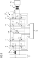
- a frequency converter 1 has a capacitor device 2.
- the capacitor device 2 may consist of a single capacitor 3 or more capacitors 3, which are connected in series and / or in parallel as needed.
- the frequency converter 1 also has an input-side inverter 4.
- the input-side inverter 4 has a number of switching paths 5, hereinafter referred to as input-side switching paths 5.
- the input-side switching paths 5 each have two series-connected semiconductor switching devices 6, hereinafter referred to as input-side semiconductor switching devices 6. Between the two input-side semiconductor switching devices 6 of the respective input-side switching path 5, a node 7 is arranged in each case, hereinafter referred to as the respective input-side node 7.
- Ends of the input side switching paths 5 are connected to the capacitor device 2.
- the input-side nodes 7 are each connected to a phase of an input-side supply network 8.
- an inductance 9 is arranged in connection with the supply network 8.
- the frequency converter 1 also has an output-side inverter 10.
- the output-side inverter 10 has a number of switching paths 11, hereinafter referred to as output-side switching paths 11.
- the output-side switching paths 11 each have two series-connected semiconductor switching devices 12, hereinafter referred to as output-side semiconductor switching devices 12. Between the two output-side semiconductor switching devices 12 of the respective output-side switching path 11, a node 13 is arranged in each case, hereinafter referred to as the respective output-side node 13.
- Ends of the output side switching paths 11 are also connected to the capacitor device 2.
- the output-side nodes 13 are each connected to a phase of a transformer 14, which is the frequency converter 1 downstream. Behind the transformer 14, a load 15 is arranged
- the frequency converter 1 is controlled by a control device 16.
- the control device 16 controls the input-side inverter 4 such that the intermediate circuit voltage UZK - ie the voltage drop across the capacitor device 2 voltage - as shown in FIG FIG. 2 as a function of time t with the amount of a sine rises and falls.
- the sine defines a base frequency f.
- the control device 16 controls the input-side inverter 4 with the base frequency f or a low integer multiple of the base frequency f, usually an odd multiple of the base frequency f, in particular three times or five times the base frequency f.
- the base frequency f corresponds to the frequency of the supply network 8. For example, it may be 16 2/3 Hz or 50 Hz.
- the amplitude of the intermediate circuit voltage UZK is determined by the voltage of the supply network 8. In particular, it can correspond approximately to the amplitude of the voltage of the supply network 8.
- the Inductance 9 causes in particular that the intermediate circuit voltage UZK may have a phase shift to the voltage of the supply network 8.
- the control device 16 further controls the output-side inverter 10 such that an alternating current I is output to the transformer 14, which at least temporarily has a frequency which is considerably greater than the base frequency f.
- the frequency is referred to below as the transformer frequency.
- the transformer frequency may be at 1 kHz or above.
- the transformer frequency can have the higher value of, for example, 1 kHz or more, if and as long as the intermediate circuit voltage UZK has a sufficiently high value, ie it is not in the vicinity of a zero crossing of the sine. In practice, it has proven to be sufficient if the instantaneous value of the intermediate circuit voltage UZK amounts to at least 5% of the amplitude of the intermediate circuit voltage UZK.
- the power supplied to the transformer 14 is composed of at least two current components.
- the other part of the current charges and discharges the capacitor device 2 of the frequency converter 1 and thereby sets a course of the intermediate circuit voltage UZK, which corresponds approximately to the mains voltage in terms of amplitude, frequency and harmonic content.
- the corresponding operation of the frequency converter 1 and the associated embodiment of the control device 16 are, for example, from the already mentioned DE 103 23 218 A1 known.
- the voltage of the supply network 8 is a high voltage.
- a rated voltage of the supply network 8 of 15 kV and a base frequency f of 16 2/3 Hz are widespread.
- Another widely used voltage system operates with a nominal voltage of 25 kV and a base frequency f of 50 Hz.
- Other voltage systems are possible and concretely known.
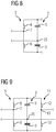
- the input-side and the output-side semiconductor switching devices 6, 12 as shown in FIGS 3 and 4 each have series circuits of a plurality of semiconductor switches 17, 18. Because the individual semiconductor switches 17, 18 are each designed for a reverse voltage, which is considerably smaller than the amplitude of the voltage of the supply network 8. For example, the individual semiconductor switches 17, 18 may be designed for a blocking voltage of 3.3 kV or 6.5 kV.
- the number of semiconductor switches 17, 18 per semiconductor switching device 6, 12 - that is, the number of each connected in series semiconductor switches 17, 18 - is determined in this case that the product of the blocking voltage of a single semiconductor switch 17, 18 with the number of semiconductor switches 17, 18 per semiconductor switching device 6, 12 is sufficiently above the maximum occurring voltage, but in any case above 10 kV.
- the semiconductor switches 18 correspond to the output-side semiconductor switching devices 12 the representation in FIG. 4 are formed as unipolar semiconductor devices based on SiC, while the semiconductor switches 17 of the input-side semiconductor switching devices 6 as shown in FIG. 3 are usually designed as SiC-IGBTs or as Si-IGBTs. Exceptionally, however, the semiconductor switches 17 of the input-side semiconductor switching devices 6 may be formed as unipolar semiconductor devices. As unipolar semiconductor devices in particular MOSFETs come into question. But there are also other types of unipolar semiconductor devices possible, such as JFETs.
- the individual semiconductor switches 17, 18 are respectively connected in parallel with one diode in parallel.
- the diodes are in the 3 and 4 for the sake of clarity not shown.
- the respective diode may be formed as a Si diode or as a SiC diode. Alternatively, it may be an independent diode or a structurally present diode of the respective semiconductor switch 17, 18.
- the frequency converter 1 according to the invention can be as shown in FIG. 5 in particular be part of an electric drive 19.
- the transformer 14 is a power converter 20 downstream.
- the power converter 20 in turn feeds at least one electrical machine 21.
- the power converter 20 is usually designed as a regenerative DC link converter. It therefore has an input-side partial converter, an output-side partial converter and a capacitor arranged between the two partial converters.
- the input-side partial converter is connected to the transformer 14, the output-side partial converter with the at least one electric machine 21.
- each output-side electrical machine 21 has its own output-side partial converter available. But it is also possible, several electric machines 21 via a common supply the output-side partial converter with electrical energy.
- the electric drive 19 as shown in the FIGS. 5 and 6 be designed as traction drive a rail vehicle 22.
- the input-side nodes 7 are usually connected to a catenary 23.
- the overhead line 23 thus forms in this case - together with a ground fault 24 - the supply network. 8
- the number of output-side switching paths 11 coincides with the number of phases of the transformer 14. Furthermore, the output side nodes 13 are each connected to one of the phases of the transformer 14. In an analogous manner, the number of input-side switching paths 5 coincides with the number of phases of the supply network 8. The input-side nodes 7 are each connected to one of the phases of the supply network 8. However, this embodiment can be modified.
- the output-side inverter 10 has only a single output-side switching path 11.
- the capacitor device 2 as shown in FIG. 7 a series connection of a plurality of capacitors 3. Between two of the series-connected capacitors 3 of the capacitor device 2, a further node 25 is arranged in this case. About this node 25, another phase of the transformer 14 is connected to the capacitor device 2.
- the input-side inverter 4 has only a single input-side switching path 5.
- the capacitor device 2 as shown in FIG. 8 a series connection of several Capacitors, wherein between two of the series-connected capacitors 3 of the capacitor device 2, a further node 25 is arranged. About this node 25, another phase of the supply network 8 is connected to the capacitor device 2.
- FIG. 7 and FIG. 8 can according to the illustration in FIG. 9 also be combined with each other.
- a frequency converter 1 has a capacitor device 2, an input-side inverter 4 and an output-side inverter 10.
- the input-side inverter 4 has input-side switching paths 5, each having two series-connected semiconductor switching devices 6 with a node 7 arranged therebetween.
- the output side inverter 10 has output-side switching paths 11, each having two series-connected semiconductor switching devices 12 with a node 13 arranged therebetween , Ends of the output-side switching paths 11 are connected to the capacitor device 2, the nodes 13 with the phases of the frequency converter 1 downstream transformer 14.
- the output-side semiconductor switching devices 12 have semiconductor switches 18 as unipolar semiconductor devices, in particular MOSFETs on.
- the present invention has many advantages.
- it is possible to keep the simple operation of the input side inverter 4 unchanged from the point of view.
- it is possible to very closely approximate the intermediate circuit voltage UZK of the ideal sinusoidal shape and thus to significantly reduce network perturbations.
- the number of series-connected semiconductor switches 17, 18 are kept low. This applies in particular to the semiconductor switches 18 of the output-side semiconductor switching devices 12.
- the switching losses can be minimized and also the transformer frequency can be increased, resulting in advantageous operating characteristics of the electric drive 19.
Abstract
Ein Frequenzumrichter (1) weist eine Kondensatoreinrichtung (2), einen eingangsseitigen Wechselrichter (4) und einen ausgangsseitigen Wechselrichter (10) auf. Der eingangsseitige Wechselrichter (4) weist eingangsseitige Schaltpfade (5) auf, die jeweils zwei in Reihe geschaltete Halbleiter-Schalteinrichtungen (6) mit einem dazwischen angeordneten Knotenpunkt (7) aufweisen. Enden der eingangsseitigen Schaltpfade (5) sind mit der Kondensatoreinrichtung (2) verbunden, die Knotenpunkte (7) mit den Phasen eines eingangsseitigen Versorgungsnetzes (8). Der ausgangsseitige Wechselrichter (10) weist ausgangsseitige Schaltpfade (11) auf, die jeweils zwei in Reihe geschaltete Halbleiter-Schalteinrichtungen (12) mit einem dazwischen angeordneten Knotenpunkt (13) aufweisen. Enden der ausgangsseitigen Schaltpfade (11) sind mit der Kondensatoreinrichtung (2) verbunden, die Knotenpunkte (13) mit den Phasen eines dem Frequenzumrichter (1) nachgeordneten Transformators (14). Die ausgangsseitigen Halbleiter-Schalteinrichtungen (12) weisen als Halbleiterschalter (18) unipolare Halbleiterbauelemente auf.A frequency converter (1) has a capacitor device (2), an input-side inverter (4) and an output-side inverter (10). The input-side inverter (4) has input-side switching paths (5), each of which has two series-connected semiconductor switching devices (6) with a node (7) arranged in between. Ends of the input-side switching paths (5) are connected to the capacitor device (2), and the nodes (7) are connected to the phases of an input-side supply network (8). The output-side inverter (10) has output-side switching paths (11), each of which has two series-connected semiconductor switching devices (12) with a node (13) arranged in between. Ends of the output-side switching paths (11) are connected to the capacitor device (2), and the nodes (13) are connected to the phases of a transformer (14) downstream of the frequency converter (1). The semiconductor switching devices (12) on the output side have unipolar semiconductor components as semiconductor switches (18).
Description
Die vorliegende Erfindung geht aus von einem Frequenzumrichter,
- wobei der Frequenzumrichter eine Kondensatoreinrichtung aufweist,
- wobei der Frequenzumrichter einen eingangsseitigen Wechselrichter aufweist, der seinerseits eine Anzahl von eingangsseitigen Schaltpfaden aufweist, die ihrerseits jeweils zwei in Reihe geschaltete eingangsseitige Halbleiter-Schalteinrichtungen und jeweils einen zwischen den beiden jeweiligen eingangsseitigen Halbleiter-Schalteinrichtungen angeordneten eingangsseitigen Knotenpunkt aufweisen,
- wobei Enden der eingangsseitigen Schaltpfade mit der Kondensatoreinrichtung verbunden sind und die eingangsseitigen Knotenpunkte jeweils mit einer Phase eines eingangsseitigen Versorgungsnetzes verbindbar sind,
- wobei der Frequenzumrichter einen ausgangsseitigen Wechselrichter aufweist, der seinerseits eine Anzahl von ausgangsseitigen Schaltpfaden aufweist, die ihrerseits jeweils zwei in Reihe geschaltete ausgangsseitige Halbleiter-Schalteinrichtungen und jeweils einen zwischen den beiden jeweiligen ausgangsseitigen Halbleiter-Schalteinrichtungen angeordneten ausgangsseitigen Knotenpunkt aufweisen,
- wobei Enden der ausgangsseitigen Schaltpfade mit der Kondensatoreinrichtung verbunden sind und die ausgangsseitigen Knotenpunkte jeweils mit einer Phase eines dem Frequenzumrichter nachgeordneten Transformators verbindbar sind.
- wherein the frequency converter comprises a capacitor device,
- wherein the frequency converter has an input-side inverter, which in turn has a number of input-side switching paths, which in turn each have two series-connected input-side semiconductor switching devices and one arranged between the two respective input-side semiconductor switching devices input-side node,
- wherein ends of the input-side switching paths are connected to the capacitor device and the input-side nodes are each connectable to a phase of an input-side supply network,
- wherein the frequency converter comprises an output side inverter, which in turn has a number of output side switching paths, which in turn each have two series-connected output-side semiconductor switching devices and in each case one output-side node arranged between the two respective output-side semiconductor switching devices,
- wherein ends of the output side switching paths are connected to the capacitor device and the output side nodes are each connectable to a phase of a frequency converter downstream of the transformer.
Die vorliegende Erfindung geht weiterhin aus von einem elektrischen Antrieb,
- wobei der elektrische Antrieb einen derartigen Frequenzumrichter aufweist,
- wobei dem Transformator ein Stromrichter nachgeordnet ist und
- wobei der Stromrichter mindestens eine elektrische Maschine speist.
- the electric drive having such a frequency converter,
- wherein the transformer is a power converter downstream and
- wherein the power converter feeds at least one electric machine.
Ein derartiger Frequenzumrichter und der zugehörige elektrische Antrieb sind beispielsweise aus der
Elektrische Eisenbahnsysteme arbeiten üblicherweise mit einer einphasigen Wechselspannung, welche elektrisch angetriebenen Schienenfahrzeugen über eine oberhalb der Geleise verlaufende Oberleitung zugeführt wird. Typisch sind eine Wechselspannung mit einer Nennspannung von 15 kV und einer Frequenz von 16 2/3 Hz oder eine Wechselspannung mit einer Nennspannung von 25 kV und einer Frequenz von 50 Hz. Es sind aber auch andere Spannungssysteme bekannt. Die hohe Wechselspannung wird gewählt, weil dadurch in der Oberleitung vergleichsweise niedrige Ströme fließen und somit elektrische Verluste minimiert werden können.Electric railway systems usually operate with a single-phase AC voltage, which is supplied to electrically powered rail vehicles via a running above the tracks overhead line. Typical are an AC voltage with a rated voltage of 15 kV and a frequency of 16 2/3 Hz or an AC voltage with a rated voltage of 25 kV and a frequency of 50 Hz. However, other voltage systems are known. The high alternating voltage is selected because this results in relatively low currents flowing in the overhead line and thus electrical losses can be minimized.
Fahrmotoren und Traktionsstromrichter von elektrischen Bahnen sind nicht für eine derart hohe Wechselspannung ausgelegt, sondern nur für wesentlich geringere Betriebsspannungen. Dadurch können insbesondere die Anforderungen an die elektrische Isolation reduziert werden. Die Wechselspannung der Oberleitung muss daher entsprechend herabgesetzt werden, bevor die elektrische Energie den Traktionsstromrichtern und den Fahrmotoren zugeführt wird. Vorzugsweise wird zugleich auch die elektrische Ausrüstung des Schienenfahrzeugs galvanisch von der Oberleitung getrennt. Dadurch führt ein Isolationsfehler beispielsweise eines Fahrmotors gegenüber dem Erdpotenzial nicht zu einem Kurzschlussstrom, sondern nur zum Auslösen einer Isolationsüberwachung.Traction motors and traction converters of electric trains are not designed for such a high AC voltage, but only for much lower operating voltages. As a result, in particular the requirements for the electrical insulation can be reduced. The AC voltage of the overhead line must therefore be reduced accordingly before the electrical energy is supplied to the traction converters and traction motors. Preferably, the electrical equipment of the rail vehicle is also galvanically separated from the overhead line at the same time. As a result, an insulation fault, for example, of a traction motor with respect to the ground potential does not lead to a short-circuit current, but only to initiate insulation monitoring.
Im konventionellen Stand der Technik wird die Wechselspannung der Fahrleitung mittels eines Transformators auf die Eingangsspannung des Traktionsstromrichters heruntergesetzt. Durch den Transformator wird zugleich auch die galvanische Trennung zwischen dem Antrieb einerseits und der Wechselspannung andererseits realisiert. Derartige Systeme benötigen - abgesehen von geeigneten Abschalt-, Filter-, Mess- und Schutzeinrichtungen primärseitig des Transformators - keine weiteren Einrichtungen.In the conventional art, the AC voltage of the catenary is lowered by means of a transformer to the input voltage of the traction converter. At the same time, the transformer also provides the galvanic isolation between the drive on the one hand and the AC voltage realized on the other hand. Such systems require - apart from suitable shutdown, filtering, measuring and protection devices on the primary side of the transformer - no other facilities.
Der Transformator des konventionellen Standes der Technik muss für die Betriebsfrequenz ausgelegt werden, welche die Wechselspannung der Oberleitung aufweist, also beispielsweise für eine Betriebsfrequenz von 16 2/3 Hz oder 50 Hz. Transformatoren, die mit derart geringen Frequenzen betrieben werden, müssen groß und schwer ausgelegt werden. Sie bestimmen in erheblichem Umfang die Fahrzeuggestaltung.The conventional prior art transformer must be designed for the operating frequency having the AC line overhead voltage, such as for an operating frequency of 16 2/3 Hz or 50 Hz. Transformers operating at such low frequencies must be large and heavy be interpreted. They determine to a considerable extent the vehicle design.
Die Wechselspannung der Oberleitung als solche kann nicht variiert werden, da dies mit erheblichem Aufwand bei der Veränderung der zu Grunde liegenden Infrastruktur verbunden wäre. Es sind jedoch verschiedene Ansätze bekannt, die Wechselspannung der Oberleitung innerhalb des Schienenfahrzeugs mittels eines Frequenzumrichters zunächst auf eine andere, erheblich höhere Frequenz umzusetzen und dem Frequenzumrichter einen Transformator nachzuordnen, beispielsweise einen Mittelfrequenztransformator für Frequenzen im Kilohertzbereich. Durch diese Ansätze können die Größe und das Gewicht des Transformators reduziert werden. Einer der Ansätze ist in der eingangs genannten
Bei der
Diese vom Ansatz her aus der
Um diese positiven Wirkungen zu erzielen, ist es jedoch erforderlich, dass die über der Kondensatoreinrichtung abfallende Zwischenkreisspannung möglichst ideal dem Betrag des Sinus folgt. Hierbei stellt sich in der Praxis das Problem, dass ein reproduzierbares Schaltverhalten der ausgangsseitigen Halbleiter-Schalteinrichtungen, die im kHz-Bereich geschaltet werden, nur dann gewährleistet werden kann, wenn die Zwischenkreisspannung einen nennenswerten Wert aufweist, meist etwa ein Drittel der maximalen Zwischenkreisspannung. Dadurch treten in der Praxis trotz der vom Ansatz her sehr vielversprechenden Vorgehensweise starke Netzrückwirkungen auf. Zur Vermeidung derartiger Netzrückwirkungen sind zusätzliche Filterkomponenten erforderlich.In order to achieve these positive effects, however, it is necessary for the DC link voltage dropping across the capacitor device to follow ideally the magnitude of the sine wave. This raises in practice the problem that a reproducible switching behavior of the output side semiconductor switching devices, which are switched in the kHz range, can only be guaranteed if the intermediate circuit voltage has a significant value, usually about one third of the maximum DC link voltage. Thus, in practice, despite the very promising approach from the beginning strong network perturbations. To avoid such network perturbations additional filter components are required.
Die Aufgabe der vorliegenden Erfindung besteht darin, Möglichkeiten zu schaffen, mittels derer ein reproduzierbares Schaltverhalten der ausgangsseitigen Halbleiter-Schalteinrichtungen auch bei einer niedrigen Zwischenkreisspannung - insbesondere weniger als 10 % der maximalen Zwischenkreisspannung - gewährleistet werden kann.The object of the present invention is to provide possibilities by means of which a reproducible switching behavior of the output-side semiconductor switching devices can be ensured even with a low DC link voltage, in particular less than 10% of the maximum DC link voltage.
Die Aufgabe wird durch einen Frequenzumrichter mit den Merkmalen des Anspruchs 1 gelöst. Vorteilhafte Ausgestaltungen des Frequenzumrichters sind Gegenstand der abhängigen Ansprüche 2 bis 8.The object is achieved by a frequency converter with the features of
Erfindungsgemäß wird ein Frequenzumrichter der eingangs genannten Art dadurch ausgestaltet, dass die ausgangsseitigen Halbleiter-Schalteinrichtungen als Halbleiterschalter unipolare Halbleiterbauelemente, insbesondere MOSFETs, aufweisen.According to the invention, a frequency converter of the type mentioned is configured in that the output side Semiconductor switching devices as a semiconductor switch unipolar semiconductor devices, in particular MOSFETs have.
Unipolare Schaltelemente weisen - im Gegensatz zu den üblicherweise verwendeten IGBTs, welche bipolare Schaltelemente sind - ein Schaltverhalten auf, das unabhängig von der mittels des jeweiligen unipolare Halbleiterbauelements geschalteten Spannung und damit unabhängig von der Zwischenkreisspannung ist.Unipolar switching elements have - in contrast to the commonly used IGBTs, which are bipolar switching elements - a switching behavior that is independent of the switched by means of the respective unipolar semiconductor device voltage and thus independent of the DC link voltage.
Beispielsweise weisen übliche MOSFETs auf Basis von Silizium (Si) eine relativ geringe Sperrspannung von nur wenigen 100 V auf, beispielsweise von ca. 600 V. Die Sperrspannung ist diejenige Spannung, die mittels des jeweiligen MOSFETs bzw. allgemein des jeweiligen Halbleiterschalters noch sicher gesperrt werden kann, die also von dem entsprechenden MOSFETs bzw. allgemein Halbleiterschalter noch sicher durchgeschaltet und auch wieder gesperrt werden kann. Wenn die Halbleiter-Schalteinrichtungen mit derartigen MOSFETs realisiert würden, wären sehr viele in Reihe geschaltete MOSFETs erforderlich, um die nötige Betriebssicherheit zu gewährleisten. Mit der Anzahl an in Reihe geschalteten Halbleiterschaltern erhöhen sich jedoch sowohl der Verdrahtungsaufwand als auch der Steuerungs- und Schaltungsaufwand enorm. Vorzugsweise sind die ausgangsseitigen Halbleiterschalter daher als unipolare Halbleiterbauelemente auf SiC-Basis ausgebildet. Unipolare Halbleiterbauelemente auf Basis von Siliziumcarbid (SiC) - beispielsweise MOSFETs - können erheblich höhere Sperrspannungen im Bereich von mehreren kV aufweisen, beispielsweise eine Sperrspannung von 3,3 kV oder 6,5 kV. Bei Verwendung derartiger unipolarer Halbleiter Schaltelemente halten sich der Verdrahtungsaufwand und der Steuerungs- und Schaltungsaufwand in vernünftigen Grenzen.For example, conventional MOSFETs based on silicon (Si) have a relatively low blocking voltage of only a few 100 V, for example of approximately 600 V. The blocking voltage is that voltage which is still reliably blocked by means of the respective MOSFET or in general the respective semiconductor switch can, that is still safely switched by the corresponding MOSFETs or general semiconductor switch and also locked again. If the semiconductor switching devices were realized with such MOSFETs, a large number of MOSFETs connected in series would be required in order to ensure the necessary operational safety. However, with the number of series-connected semiconductor switches, both the wiring complexity and the control and circuit complexity increase enormously. The output-side semiconductor switches are therefore preferably designed as SiC-based unipolar semiconductor components. Unipolar semiconductor devices based on silicon carbide (SiC) - for example MOSFETs - can have significantly higher blocking voltages in the range of several kV, for example a blocking voltage of 3.3 kV or 6.5 kV. When using such unipolar semiconductor switching elements, the wiring costs and the control and circuit complexity keep within reasonable limits.
Die eingangsseitigen Halbleiter-Schalteinrichtungen können hingegen als Halbleiterschalter nach Bedarf unipolare Halbleiterbauelemente auf SiC-Basis oder - wie im Stand der Technik auch - SiC-IGBTs oder Si-IGBTs aufweisen. Die Verwendung von IGBTs auf Si- oder SiC-Basis auf der Eingangsseite des Frequenzumrichters ist unkritisch, weil die Halbleiter-Schalteinrichtungen auf der Eingangsseite mit einer erheblich niedrigeren Taktrate als die Halbleiter-Schalteinrichtungen auf der Ausgangsseite des Wechselrichters geschaltet werden.On the other hand, the input-side semiconductor switching devices may, as semiconductor switches, comprise SiC-based, unipolar semiconductor devices or, as in the prior art, SiC-IGBTs or Si-IGBTs. The usage of Si or SiC based IGBTs on the input side of the frequency converter is not critical because the semiconductor switching devices on the input side are switched at a significantly lower clock rate than the semiconductor switching devices on the output side of the inverter.
In der Regel liegt die Nennspannung des Versorgungsnetzes im Bereich von etlichen kV, beispielsweise bei 15 kV oder 25 kV. In derartigen Fällen weisen die eingangsseitigen und die ausgangsseitigen Halbleiter-Schalteinrichtungen jeweils Reihenschaltungen von mehreren Halbleiterschaltern auf. Die einzelnen Halbleiterschalter sind jeweils für eine Sperrspannung ausgelegt. Die Anzahl an Halbleiterschaltern pro Halbleiter-Schalteinrichtung ist derart bestimmt, dass das Produkt der Sperrspannung mit der Anzahl an Halbleiterschaltern pro Halbleiter-Schalteinrichtung in hinreichendem Umfang oberhalb der Amplitude der Spannung des Versorgungsnetzes liegt. In der Praxis bedeutet dies - allgemein gesprochen - in aller Regel eine Spannung oberhalb von 10 kV.As a rule, the rated voltage of the supply network is in the range of several kV, for example at 15 kV or 25 kV. In such cases, the input-side and the output-side semiconductor switching devices each have series circuits of a plurality of semiconductor switches. The individual semiconductor switches are each designed for a blocking voltage. The number of semiconductor switches per semiconductor switching device is determined such that the product of the blocking voltage with the number of semiconductor switches per semiconductor switching device is sufficiently above the amplitude of the voltage of the supply network. In practice, this means - generally speaking - usually a voltage above 10 kV.
Wenn beispielsweise die Sperrspannung eines einzelnen Halbleiterschalters 3,3 kV beträgt und hiervon nur etwa 2/3 genutzt werden sollen und weiterhin die Nennspannung 15 kV beträgt, müssen zwölf Halbleiterschalter in Reihe geschaltet werden. Bei einer Nennspannung von 25 kV muss die Anzahl an Halbleiterschaltern pro Halbleiter-Schalteinrichtung entsprechend höher gewählt sein. Wenn alternativ beispielsweise die Sperrspannung eines einzelnen Halbleiterschalters 6,5 kV beträgt, müssen bei einer Nennspannung von 25 kV mindestens acht, besser neun oder zehn, Halbleiterschalter in Reihe geschaltet werden. Bei anderen Nennspannungen und anderen Sperrspannungen und anderen Sicherheitsreserven ergeben sich andere Werte, das Berechnungsschema bleibt aber das gleiche.For example, if the blocking voltage of a single semiconductor switch is 3.3 kV and only about 2/3 of it is to be used and still the rated voltage is 15 kV, twelve semiconductor switches must be connected in series. At a rated voltage of 25 kV, the number of semiconductor switches per semiconductor switching device must be selected correspondingly higher. Alternatively, if, for example, the blocking voltage of a single semiconductor switch is 6.5 kV, at a rated voltage of 25 kV at least eight, better nine or ten, semiconductor switches must be connected in series. At other rated voltages and other reverse voltages and other safety margins, other values result, but the calculation scheme remains the same.
Es ist weiterhin von Vorteil, den Halbleiterschaltern Überbrückungsschalter parallel zu schalten. Die Überbrückungsschalter sind im Regelfall geöffnet, so dass der jeweilige Halbleiterschalter seine Funktion als Schaltelement erfüllen kann. Falls einer der Halbleiterschalter defekt wird, kann der jeweilige Überbrückungsschalter aber auch geschlossen werden, so dass er den jeweiligen Halbleiterschalter überbrückt. Dadurch wird ein Weiterbetrieb des Frequenzumrichters trotz des defekten Halbleiterschalters ermöglicht. Die Gesamtzahl an in Reihe geschalteten Halbleiterschaltern muss in diesem Fall selbstverständlich entsprechend erhöht werden.It is also advantageous to switch the semiconductor switches bypass switch in parallel. The bypass switches are normally open, so that the respective semiconductor switch fulfill its function as a switching element can. If one of the semiconductor switches is defective, however, the respective bypass switch can also be closed, so that it bridges the respective semiconductor switch. This allows continued operation of the frequency converter despite the defective semiconductor switch. The total number of series-connected semiconductor switches must of course be increased accordingly in this case.
Bezüglich der Ausgestaltung des ausgangsseitigen Wechselrichters sind zwei Alternativen möglich.With regard to the configuration of the output-side inverter, two alternatives are possible.
Zum einen ist es möglich, dass die Anzahl an ausgangsseitigen Schaltpfaden mit der Anzahl an Phasen des Transformators übereinstimmt und dass die Knotenpunkte der ausgangsseitigen Schaltpfade jeweils mit einer der Phasen des Transformators verbindbar sind. Diese Ausgestaltung ist sowohl bei einem (einphasigen) Wechselspannungstransformator als auch bei einem mehrphasigen Drehspannungstransformator realisierbar.On the one hand, it is possible that the number of output-side switching paths coincides with the number of phases of the transformer, and that the nodes of the output-side switching paths can each be connected to one of the phases of the transformer. This refinement can be implemented both in the case of a (single-phase) AC voltage transformer and in the case of a polyphase three-phase voltage transformer.
Zum anderen ist es möglich, dass der ausgangsseitige Wechselrichter nur einen einzelnen ausgangsseitigen Schaltpfad aufweist, dass die Kondensatoreinrichtung eine Reihenschaltung von mehreren Kondensatoren aufweist und dass zwischen zwei der in Reihe geschalteten Kondensatoren der Kondensatoreinrichtung ein weiterer Knotenpunkt angeordnet ist, über den eine weitere Phase des Transformators mit der Kondensatoreinrichtung verbindbar ist. Diese Ausgestaltung ist nur bei einem (einphasigen) Wechselspannungstransformator realisierbar. Bei dieser Ausgestaltung des Frequenzumrichters verdoppelt sich gegenüber der Ausgestaltung, bei der die Anzahl an ausgangsseitigen Schaltpfaden mit der Anzahl an Phasen des Transformators übereinstimmt, die Zwischenkreisspannung. Demzufolge muss pro Halbleiterschalteinrichtung auch die Anzahl an in Reihe geschalteten Halbleiterschaltern entsprechend erhöht werden.On the other hand, it is possible that the output-side inverter has only a single output-side switching path, that the capacitor device comprises a series connection of a plurality of capacitors and that between two of the series-connected capacitors of the capacitor device, a further node is arranged, via which a further phase of the transformer can be connected to the capacitor device. This embodiment can only be realized with a (single-phase) AC voltage transformer. In this embodiment of the frequency converter doubled compared to the embodiment in which the number of output-side switching paths with the number of phases of the transformer, the intermediate circuit voltage. Consequently, the number of semiconductor switches connected in series must also be increased correspondingly per semiconductor switching device.
In analoger Weise sind auch bezüglich der Ausgestaltung des eingangsseitigen Wechselrichters zwei Alternativen möglich.In an analogous manner, two alternatives are also possible with regard to the configuration of the input-side inverter.
Zum einen ist es möglich, dass die Anzahl an eingangsseitigen Schaltpfaden mit der Anzahl an Phasen des Versorgungsnetzes übereinstimmt und dass die Knotenpunkte der eingangsseitigen Schaltpfade jeweils mit einer der Phasen des Versorgungsnetzes verbindbar sind.On the one hand, it is possible that the number of input-side switching paths coincides with the number of phases of the supply network and that the nodes of the input-side switching paths can each be connected to one of the phases of the supply network.
Zum anderen ist es möglich, dass der eingangsseitige Wechselrichter nur einen einzelnen eingangsseitigen Schaltpfad aufweist, dass die Kondensatoreinrichtung eine Reihenschaltung von mehreren Kondensatoren aufweist und dass zwischen zwei der in Reihe geschalteten Kondensatoren der Kondensatoreinrichtung ein weiterer Knotenpunkt angeordnet ist, über den eine weitere Phase des Versorgungsnetzes mit der Kondensatoreinrichtung verbindbar ist. Auch bei dieser Ausgestaltung des Frequenzumrichters verdoppelt sich gegenüber der Ausgestaltung, bei der die Anzahl an eingangsseitigen Schaltpfaden mit der Anzahl an Phasen des Versorgungsnetzes übereinstimmt, die Zwischenkreisspannung. Auch hier muss daher pro Halbleiter-schalteinrichtung die Anzahl an in Reihe geschalteten Halbleiterschaltern entsprechend erhöht werden.On the other hand, it is possible that the input-side inverter has only a single input-side switching path, that the capacitor device comprises a series connection of a plurality of capacitors and that between two of the series-connected capacitors of the capacitor device, a further node is arranged, via which a further phase of the supply network can be connected to the capacitor device. Also in this embodiment of the frequency converter doubled compared to the embodiment in which the number of input-side switching paths matches the number of phases of the supply network, the intermediate circuit voltage. Again, therefore, the number of series-connected semiconductor switches must be increased accordingly per semiconductor switching device.
Die Aufgabe wird weiterhin durch einen elektrischen Antrieb mit den Merkmalen des Anspruchs 9 gelöst. Eine vorteilhafte Ausgestaltung ist Gegenstand des abhängigen Anspruchs 10.The object is further achieved by an electric drive with the features of claim 9. An advantageous embodiment is the subject of the dependent claim 10th
Erfindungsgemäß ist bei einem elektrischen Antrieb der eingangs genannten Art der Frequenzumrichter erfindungsgemäß ausgebildet.According to the invention is formed according to the invention in an electric drive of the type mentioned in the frequency converter.
Der elektrische Antrieb kann insbesondere als Traktionsantrieb eines Schienenfahrzeugs ausgebildet sein. In diesem Fall sind die eingangsseitigen Knotenpunkte in der Regel mit einem als Oberleitungsnetz ausgebildeten Versorgungsnetz verbindbar.The electric drive can be designed in particular as a traction drive of a rail vehicle. In this case, the input-side nodes are usually connectable to a trained as a trolley network supply network.
Die oben beschriebenen Eigenschaften, Merkmale und Vorteile dieser Erfindung sowie die Art und Weise, wie diese erreicht werden, werden klarer und deutlicher verständlich im Zusammenhang mit der folgenden Beschreibung der Ausführungsbeispiele, die in Verbindung mit den Zeichnungen näher erläutert werden. Hierbei zeigen in schematischer Darstellung:
- FIG 1
- einen Frequenzumrichter,
- FIG 2
- ein Zeitdiagramm,
- FIG 3
- eine eingangsseitige Halbleiter-Schalteinrichtung,
- FIG 4
- eine ausgangsseitige Halbleiter-Schalteinrichtung,
- FIG 5
- einen elektrischen Antrieb,
- FIG 6
- ein Schienenfahrzeug,
- FIG 7
- einen weiteren Frequenzumrichter,
- FIG 8
- einen weiteren Frequenzumrichter und
- FIG 9
- einen weiteren Frequenzumrichter.
- FIG. 1
- a frequency converter,
- FIG. 2
- a time diagram,
- FIG. 3
- an input-side semiconductor switching device,
- FIG. 4
- an output side semiconductor switching device,
- FIG. 5
- an electric drive,
- FIG. 6
- a rail vehicle,
- FIG. 7
- another frequency converter,
- FIG. 8
- another frequency converter and
- FIG. 9
- another frequency converter.
Gemäß
Der Frequenzumrichter 1 weist weiterhin einen eingangsseitigen Wechselrichter 4 auf. Der eingangsseitige Wechselrichter 4 weist eine Anzahl von Schaltpfaden 5 auf, nachfolgend als eingangsseitige Schaltpfade 5 bezeichnet. Die eingangsseitigen Schaltpfade 5 weisen jeweils zwei in Reihe geschaltete Halbleiter-Schalteinrichtungen 6 auf, nachfolgend als eingangsseitige Halbleiter-Schalteinrichtungen 6 bezeichnet. Zwischen den beiden eingangsseitigen Halbleiter-Schalteinrichtungen 6 des jeweiligen eingangsseitigen Schaltpfades 5 ist jeweils ein Knotenpunkt 7 angeordnet, nachfolgend als jeweiliger eingangsseitiger Knotenpunkt 7 bezeichnet.The
Enden der eingangsseitigen Schaltpfade 5 sind mit der Kondensatoreinrichtung 2 verbunden. Die eingangsseitigen Knotenpunkte 7 sind jeweils mit einer Phase eines eingangsseitigen Versorgungsnetzes 8 verbunden. In der Regel ist in der Verbindung mit dem Versorgungsnetz 8 eine Induktivität 9 angeordnet.Ends of the input
Der Frequenzumrichter 1 weist weiterhin einen ausgangsseitigen Wechselrichter 10 auf. Der ausgangsseitige Wechselrichter 10 weist eine Anzahl von Schaltpfaden 11 auf, nachfolgend als ausgangsseitige Schaltpfade 11 bezeichnet. Die ausgangsseitigen Schaltpfade 11 weisen jeweils zwei in Reihe geschaltete Halbleiter-Schalteinrichtungen 12 auf, nachfolgend als ausgangsseitige Halbleiter-Schalteinrichtungen 12 bezeichnet. Zwischen den beiden ausgangsseitigen Halbleiter-Schalteinrichtungen 12 des jeweiligen ausgangsseitigen Schaltpfades 11 ist jeweils ein Knotenpunkt 13 angeordnet, nachfolgend als jeweiliger ausgangsseitiger Knotenpunkt 13 bezeichnet.The
Enden der ausgangsseitigen Schaltpfade 11 sind ebenfalls mit der Kondensatoreinrichtung 2 verbunden. Die ausgangsseitigen Knotenpunkte 13 sind jeweils mit einer Phase eines Transformators 14 verbunden, welcher dem Frequenzumrichter 1 nachgeordnet ist. Hinter dem Transformator 14 ist eine Last 15 angeordnetEnds of the output
Der Frequenzumrichter 1 wird von einer Steuereinrichtung 16 gesteuert.The
Die Steuereinrichtung 16 steuert den eingangsseitigen Wechselrichter 4 derart, dass die Zwischenkreisspannung UZK - also die über der Kondensatoreinrichtung 2 abfallende Spannung - entsprechend der Darstellung in
Die Steuereinrichtung 16 steuert weiterhin den ausgangsseitigen Wechselrichter 10 derart, dass an den Transformator 14 ein Wechselstrom I abgegeben wird, der zumindest temporär eine Frequenz aufweist, die erheblich größer als die Basisfrequenz f ist. Die Frequenz wird nachfolgend als Transformatorfrequenz bezeichnet. Die Transformatorfrequenz kann insbesondere bei 1 kHz oder darüber liegen. Die Transformatorfrequenz kann insbesondere dann und solange den höheren Wert von beispielsweise 1 kHz oder darüber aufweisen, wenn und solange die Zwischenkreisspannung UZK einen hinreichend hohen Wert aufweist, sich also nicht in der Nähe eines Nulldurchgangs des Sinus befindet. In der Praxis hat es sich als ausreichend erwiesen, wenn die der momentane Wert der Zwischenkreisspannung UZK mindestens 5 % der Amplitude der Zwischenkreisspannung UZK beträgt.The
Der dem Transformator 14 zugeführte Strom setzt sich aus mindestens zwei Stromanteilen zusammen. Der eine Stromanteil dient der Übertragung der Energie zur Last 15. Der andere Stromanteil lädt und entlädt die Kondensatoreinrichtung 2 des Frequenzumrichters 1 und stellt dadurch einen Verlauf der Zwischenkreisspannung UZK ein, der in Amplitude, Frequenz und Oberschwingungsanteil etwa der Netzspannung entspricht.The power supplied to the
Der entsprechende Betrieb des Frequenzumrichters 1 und die zugehörige Ausgestaltung der Steuereinrichtung 16 sind beispielsweise aus der bereits erwähnten
In vielen Fällen ist die Spannung des Versorgungsnetzes 8 eine Hochspannung. Beispielsweise bei Bahnsystemen sind eine Nennspannung des Versorgungsnetzes 8 von 15 kV und eine Basisfrequenz f von 16 2/3 Hz weit verbreitet. Ein ebenfalls weit verbreitetes Spannungssystem arbeitet mit einer Nennspannung von 25 kV und einer Basisfrequenz f von 50 Hz. Auch andere Spannungssysteme sind möglich und konkret auch bekannt.In many cases, the voltage of the supply network 8 is a high voltage. For example, in railway systems, a rated voltage of the supply network 8 of 15 kV and a base frequency f of 16 2/3 Hz are widespread. Another widely used voltage system operates with a nominal voltage of 25 kV and a base frequency f of 50 Hz. Other voltage systems are possible and concretely known.
Im Falle derart hoher Spannungen - in jedem Fall oberhalb von 10 kV - ist es erforderlich, dass die eingangsseitigen und die ausgangsseitigen Halbleiter-Schalteinrichtungen 6, 12 entsprechend der Darstellung in den
Unabhängig von der Anzahl an in Reihe geschalteten Halbleiterschaltern 17, 18 gibt es aber einen wichtigen Unterschied zwischen den Halbleiterschaltern 17 der eingangsseitigen Halbleiter-Schalteinrichtungen 6 und den Halbleiterschaltern 18 der ausgangsseitigen Halbleiter-Schalteinrichtungen 12. Dieser Unterschied gilt nicht nur im Regelfall, in dem die Reihenschaltungen, welche die jeweilige Halbleiter-Schalteinrichtung 6, 12 bilden, jeweils mehrere in Reihe geschaltete Halbleiter 17, 18 aufweisen. Der Unterschied gilt auch in dem Spezialfall, in dem die jeweilige Halbleiter-Schalteinrichtung 6, 12 ausnahmsweise nur einen einzigen Halbleiterschalter 17, 18 aufweist, die Reihenschaltung also entartet ist.However, regardless of the number of series-connected semiconductor switches 17, 18, there is an important difference between the semiconductor switches 17 of the input-side
Der Unterschied besteht darin, dass die Halbleiterschalter 18 der ausgangsseitigen Halbleiter-Schalteinrichtungen 12 entsprechend der Darstellung in
Den einzelnen Halbleiterschaltern 17, 18 ist, wie Fachleuten allgemein bekannt ist, jeweils eine Diode parallel gegengeschaltet. Die Dioden sind in den
Der erfindungsgemäße Frequenzumrichter 1 kann entsprechend der Darstellung in
Insbesondere kann der elektrische Antrieb 19 entsprechend der Darstellung in den
In der bisher erläuterten Ausgestaltung des Frequenzumrichters 1 stimmt die Anzahl an ausgangsseitigen Schaltpfaden 11 mit der Anzahl an Phasen des Transformators 14 überein. Weiterhin sind die ausgangsseitigen Knotenpunkte 13 jeweils mit einer der Phasen des Transformators 14 verbunden. In analoger Weise stimmt die Anzahl an eingangsseitigen Schaltpfaden 5 mit der Anzahl an Phasen des Versorgungsnetzes 8 überein. Auch sind die eingangsseitigen Knotenpunkte 7 jeweils mit einer der Phasen des Versorgungsnetzes 8 verbunden. Diese Ausgestaltung kann jedoch modifiziert werden.In the embodiment of the
So ist es beispielsweise entsprechend der Darstellung in
In analoger Weise ist es entsprechend der Darstellung in
Die Ausgestaltungen gemäß
Zusammengefasst betrifft die vorliegende Erfindung somit folgenden Sachverhalt:
Ein Frequenzumrichter 1 weist eine Kondensatoreinrichtung 2, einen eingangsseitigen Wechselrichter 4 und einen ausgangsseitigen Wechselrichter 10 auf. Der eingangsseitige Wechselrichter 4 weist eingangsseitige Schaltpfade 5 auf, die jeweils zwei in Reihe geschaltete Halbleiter-Schalteinrichtungen 6 mit einem dazwischen angeordneten Knotenpunkt 7 aufweisen. Enden der eingangsseitigen Schaltpfade 5 sind mit der Kondensatoreinrichtung 2 verbunden, die Knotenpunkte 7 mit den Phasen eines eingangsseitigen Versorgungsnetzes 8. Der ausgangsseitige Wechselrichter 10 weist ausgangsseitige Schaltpfade 11 auf, die jeweils zwei in Reihe geschaltete Halbleiter-Schalteinrichtungen 12 mit einem dazwischen angeordneten Knotenpunkt 13 aufweisen. Enden der ausgangsseitigen Schaltpfade 11 sind mit der Kondensatoreinrichtung 2 verbunden, die Knotenpunkte 13 mit den Phasen eines dem Frequenzumrichter 1 nachgeordneten Transformators 14. Die ausgangsseitigen Halbleiter-Schalteinrichtungen 12 weisen als Halbleiterschalter 18 unipolare Halbleiterbauelemente, insbesondere MOSFETs, auf.In summary, the present invention thus relates to the following facts:
A
Die vorliegende Erfindung weist viele Vorteile auf. Insbesondere ist es möglich, den einfachen Betrieb des eingangsseitigen Wechselrichters 4 vom Ansatz her unverändert beizubehalten. Weiterhin ist es möglich, die Zwischenkreisspannung UZK der idealen Sinusform sehr weitgehend anzunähern und damit Netzrückwirkungen deutlich zu reduzieren. Schließlich kann insbesondere die Anzahl an in Reihe geschalteten Halbleiterschaltern 17, 18 gering gehalten werden. Dies gilt insbesondere für die Halbleiterschalter 18 der ausgangsseitigen Halbleiter-Schalteinrichtungen 12. Schließlich können die Schaltverluste minimiert werden und kann auch die Transformatorfrequenz erhöht werden, wodurch sich vorteilhafte Betriebseigenschaften des elektrischen Antriebs 19 ergeben.The present invention has many advantages. In particular, it is possible to keep the simple operation of the input side inverter 4 unchanged from the point of view. Furthermore, it is possible to very closely approximate the intermediate circuit voltage UZK of the ideal sinusoidal shape and thus to significantly reduce network perturbations. Finally, can In particular, the number of series-connected semiconductor switches 17, 18 are kept low. This applies in particular to the semiconductor switches 18 of the output-side
Obwohl die Erfindung im Detail durch das bevorzugte Ausführungsbeispiel näher illustriert und beschrieben wurde, so ist die Erfindung nicht durch die offenbarten Beispiele eingeschränkt und andere Variationen können vom Fachmann hieraus abgeleitet werden, ohne den Schutzumfang der Erfindung zu verlassen.Although the invention has been further illustrated and described in detail by the preferred embodiment, the invention is not limited by the disclosed examples, and other variations can be derived therefrom by those skilled in the art without departing from the scope of the invention.
Claims (10)
Priority Applications (1)
| Application Number | Priority Date | Filing Date | Title |
|---|---|---|---|
| EP18174782.5A EP3576278A1 (en) | 2018-05-29 | 2018-05-29 | Frequency inverter |
Applications Claiming Priority (1)
| Application Number | Priority Date | Filing Date | Title |
|---|---|---|---|
| EP18174782.5A EP3576278A1 (en) | 2018-05-29 | 2018-05-29 | Frequency inverter |
Publications (1)
| Publication Number | Publication Date |
|---|---|
| EP3576278A1 true EP3576278A1 (en) | 2019-12-04 |
Family
ID=62492428
Family Applications (1)
| Application Number | Title | Priority Date | Filing Date |
|---|---|---|---|
| EP18174782.5A Withdrawn EP3576278A1 (en) | 2018-05-29 | 2018-05-29 | Frequency inverter |
Country Status (1)
| Country | Link |
|---|---|
| EP (1) | EP3576278A1 (en) |
Citations (4)
| Publication number | Priority date | Publication date | Assignee | Title |
|---|---|---|---|---|
| DE10323218A1 (en) | 2003-05-22 | 2004-12-16 | Siemens Ag | High voltage converter for rail traction, is formed from input current converter based on series-connected power semiconductor switches, intermediate circuit and high-voltage inverter |
| DE102005042319A1 (en) * | 2005-09-06 | 2007-03-08 | Siemens Ag | Large voltage converter with network side converter, has n circuit boost-buck converter device which has n load side converters and n transformers |
| WO2012098107A2 (en) * | 2011-01-17 | 2012-07-26 | Abb Technology Ag | Converter circuit with a charging unit |
| US20180064001A1 (en) * | 2016-08-26 | 2018-03-01 | Enrique Ledezma | Modular Size Multi-Megawatt Silicon Carbide-Based Medium Voltage Conversion System |
-
2018
- 2018-05-29 EP EP18174782.5A patent/EP3576278A1/en not_active Withdrawn
Patent Citations (4)
| Publication number | Priority date | Publication date | Assignee | Title |
|---|---|---|---|---|
| DE10323218A1 (en) | 2003-05-22 | 2004-12-16 | Siemens Ag | High voltage converter for rail traction, is formed from input current converter based on series-connected power semiconductor switches, intermediate circuit and high-voltage inverter |
| DE102005042319A1 (en) * | 2005-09-06 | 2007-03-08 | Siemens Ag | Large voltage converter with network side converter, has n circuit boost-buck converter device which has n load side converters and n transformers |
| WO2012098107A2 (en) * | 2011-01-17 | 2012-07-26 | Abb Technology Ag | Converter circuit with a charging unit |
| US20180064001A1 (en) * | 2016-08-26 | 2018-03-01 | Enrique Ledezma | Modular Size Multi-Megawatt Silicon Carbide-Based Medium Voltage Conversion System |
Non-Patent Citations (2)
| Title |
|---|
| DIECKERHOFF S ET AL: "Evaluation of IGBTB multilevel converters for transformerless traction applications", PESC'03. 2003 IEEE 34TH. ANNUAL POWER ELECTRONICS SPECIALISTS CONFERENCE. CONFERENCE PROCEEDINGS. ACAPULCO, MEXICO, JUNE 15 - 19, 2003; [ANNUAL POWER ELECTRONICS SPECIALISTS CONFERENCE], NEW YORK, NY :; IEEE, US, vol. 4, 15 June 2003 (2003-06-15), pages 1757 - 1763, XP010648560, ISBN: 978-0-7803-7754-7, DOI: 10.1109/PESC.2003.1217721 * |
| VECHALAPU KASUNAIDU ET AL: "High-speed medium voltage (MV) drive applications enabled by series connection of 1.7 kV SiC MOSFET devices", 2017 IEEE ENERGY CONVERSION CONGRESS AND EXPOSITION (ECCE), IEEE, 1 October 2017 (2017-10-01), pages 808 - 815, XP033246884, DOI: 10.1109/ECCE.2017.8095868 * |
Similar Documents
| Publication | Publication Date | Title |
|---|---|---|
| EP2671297B1 (en) | Method for clearing a fault on a hvdc line, arrangement for transmission of electrical current over a hvdc line and converter | |
| EP1922803B1 (en) | Device for electron energy transfer | |
| EP2898595B1 (en) | Modulat multilevel dc/dc converter for hvdc applications | |
| EP3120451B1 (en) | Power supply for a non-linear load with multi-level matrix converters | |
| DE102008014898A1 (en) | Method for controlling a multiphase power converter with distributed energy stores at low output frequencies | |
| EP2617114B1 (en) | Current supply unit for a nonlinear time-varialbe load | |
| DE102008007658A1 (en) | Static converter | |
| EP2845288B1 (en) | On- or off-coupling of power in a branch at a node of a dc network by a voltage source connected in series | |
| EP0166954A1 (en) | Method for the reduction of dynamic overvoltages in an alternating current grid system | |
| CH715448A2 (en) | Multi-phase converter topology for multi-phase and single-phase operation. | |
| EP2845303B1 (en) | Power converter and operating method for converting voltages | |
| DE102005019215A1 (en) | Output filter for e.g. pulsed power converter, has filter chokes and filter condensers, which are interconnected as LC low pass, and circuit arrangement for dynamically and continuously reducing effectiveness of filter chokes and condensers | |
| EP2067227B1 (en) | Drive energy supply in rail vehicles | |
| DE102011005905B4 (en) | Switch for a transmission link for high-voltage direct current | |
| EP3251194B1 (en) | Energy storage arrangement | |
| EP3478527B1 (en) | Bidirectional onboard electrical power converter and method of operating the same | |
| EP3622621B1 (en) | Multilevel power converter | |
| WO2017157614A1 (en) | Modular multi-stage converter | |
| EP2966769B1 (en) | Operation of a modular multi level power converter | |
| EP3576278A1 (en) | Frequency inverter | |
| EP3180844B1 (en) | Power converter arrangement with short-circuit unit and method for separating an ac voltage line | |
| DE102019105196B4 (en) | Method for current limitation in the event of transient voltage changes at an AC output of a multilevel inverter and multilevel inverter | |
| WO2018113926A1 (en) | Power converter | |
| EP3741023B1 (en) | Device and method for controlling a load flow in an alternating-voltage network | |
| EP0642201A1 (en) | High voltage direct current transmission system |
Legal Events
| Date | Code | Title | Description |
|---|---|---|---|
| PUAI | Public reference made under article 153(3) epc to a published international application that has entered the european phase |
Free format text: ORIGINAL CODE: 0009012 |
|
| AK | Designated contracting states |
Kind code of ref document: A1 Designated state(s): AL AT BE BG CH CY CZ DE DK EE ES FI FR GB GR HR HU IE IS IT LI LT LU LV MC MK MT NL NO PL PT RO RS SE SI SK SM TR |
|
| AX | Request for extension of the european patent |
Extension state: BA ME |
|
| STAA | Information on the status of an ep patent application or granted ep patent |
Free format text: STATUS: THE APPLICATION IS DEEMED TO BE WITHDRAWN |
|
| 18D | Application deemed to be withdrawn |
Effective date: 20200605 |