EP3300242B1 - Regulation of a three-level inverter - Google Patents
Regulation of a three-level inverter Download PDFInfo
- Publication number
- EP3300242B1 EP3300242B1 EP16190787.8A EP16190787A EP3300242B1 EP 3300242 B1 EP3300242 B1 EP 3300242B1 EP 16190787 A EP16190787 A EP 16190787A EP 3300242 B1 EP3300242 B1 EP 3300242B1
- Authority
- EP
- European Patent Office
- Prior art keywords
- space
- hysteresis
- phase
- level inverter
- voltage
- Prior art date
- Legal status (The legal status is an assumption and is not a legal conclusion. Google has not performed a legal analysis and makes no representation as to the accuracy of the status listed.)
- Active
Links
- 230000001105 regulatory effect Effects 0.000 claims description 22
- 238000000034 method Methods 0.000 claims description 18
- 230000007704 transition Effects 0.000 claims description 14
- 101000934888 Homo sapiens Succinate dehydrogenase cytochrome b560 subunit, mitochondrial Proteins 0.000 claims description 8
- 102100025393 Succinate dehydrogenase cytochrome b560 subunit, mitochondrial Human genes 0.000 claims description 8
- 239000013598 vector Substances 0.000 description 126
- 238000010586 diagram Methods 0.000 description 18
- 239000003990 capacitor Substances 0.000 description 7
- 229910003460 diamond Inorganic materials 0.000 description 6
- 239000010432 diamond Substances 0.000 description 6
- 230000000694 effects Effects 0.000 description 4
- 230000001276 controlling effect Effects 0.000 description 3
- 241001270131 Agaricus moelleri Species 0.000 description 2
- 230000005284 excitation Effects 0.000 description 2
- 230000010355 oscillation Effects 0.000 description 2
- 230000003071 parasitic effect Effects 0.000 description 2
- 241001136792 Alle Species 0.000 description 1
- 230000015572 biosynthetic process Effects 0.000 description 1
- 230000008878 coupling Effects 0.000 description 1
- 238000010168 coupling process Methods 0.000 description 1
- 238000005859 coupling reaction Methods 0.000 description 1
- 230000001419 dependent effect Effects 0.000 description 1
- 230000011664 signaling Effects 0.000 description 1
Images

Classifications
-
- H—ELECTRICITY
- H02—GENERATION; CONVERSION OR DISTRIBUTION OF ELECTRIC POWER
- H02M—APPARATUS FOR CONVERSION BETWEEN AC AND AC, BETWEEN AC AND DC, OR BETWEEN DC AND DC, AND FOR USE WITH MAINS OR SIMILAR POWER SUPPLY SYSTEMS; CONVERSION OF DC OR AC INPUT POWER INTO SURGE OUTPUT POWER; CONTROL OR REGULATION THEREOF
- H02M7/00—Conversion of ac power input into dc power output; Conversion of dc power input into ac power output
- H02M7/42—Conversion of dc power input into ac power output without possibility of reversal
- H02M7/44—Conversion of dc power input into ac power output without possibility of reversal by static converters
- H02M7/48—Conversion of dc power input into ac power output without possibility of reversal by static converters using discharge tubes with control electrode or semiconductor devices with control electrode
- H02M7/483—Converters with outputs that each can have more than two voltages levels
- H02M7/487—Neutral point clamped inverters
-
- H—ELECTRICITY
- H02—GENERATION; CONVERSION OR DISTRIBUTION OF ELECTRIC POWER
- H02M—APPARATUS FOR CONVERSION BETWEEN AC AND AC, BETWEEN AC AND DC, OR BETWEEN DC AND DC, AND FOR USE WITH MAINS OR SIMILAR POWER SUPPLY SYSTEMS; CONVERSION OF DC OR AC INPUT POWER INTO SURGE OUTPUT POWER; CONTROL OR REGULATION THEREOF
- H02M7/00—Conversion of ac power input into dc power output; Conversion of dc power input into ac power output
- H02M7/42—Conversion of dc power input into ac power output without possibility of reversal
- H02M7/44—Conversion of dc power input into ac power output without possibility of reversal by static converters
- H02M7/48—Conversion of dc power input into ac power output without possibility of reversal by static converters using discharge tubes with control electrode or semiconductor devices with control electrode
- H02M7/53—Conversion of dc power input into ac power output without possibility of reversal by static converters using discharge tubes with control electrode or semiconductor devices with control electrode using devices of a triode or transistor type requiring continuous application of a control signal
- H02M7/537—Conversion of dc power input into ac power output without possibility of reversal by static converters using discharge tubes with control electrode or semiconductor devices with control electrode using devices of a triode or transistor type requiring continuous application of a control signal using semiconductor devices only, e.g. single switched pulse inverters
- H02M7/5387—Conversion of dc power input into ac power output without possibility of reversal by static converters using discharge tubes with control electrode or semiconductor devices with control electrode using devices of a triode or transistor type requiring continuous application of a control signal using semiconductor devices only, e.g. single switched pulse inverters in a bridge configuration
- H02M7/53871—Conversion of dc power input into ac power output without possibility of reversal by static converters using discharge tubes with control electrode or semiconductor devices with control electrode using devices of a triode or transistor type requiring continuous application of a control signal using semiconductor devices only, e.g. single switched pulse inverters in a bridge configuration with automatic control of output voltage or current
- H02M7/53875—Conversion of dc power input into ac power output without possibility of reversal by static converters using discharge tubes with control electrode or semiconductor devices with control electrode using devices of a triode or transistor type requiring continuous application of a control signal using semiconductor devices only, e.g. single switched pulse inverters in a bridge configuration with automatic control of output voltage or current with analogue control of three-phase output
- H02M7/53876—Conversion of dc power input into ac power output without possibility of reversal by static converters using discharge tubes with control electrode or semiconductor devices with control electrode using devices of a triode or transistor type requiring continuous application of a control signal using semiconductor devices only, e.g. single switched pulse inverters in a bridge configuration with automatic control of output voltage or current with analogue control of three-phase output based on synthesising a desired voltage vector via the selection of appropriate fundamental voltage vectors, and corresponding dwelling times
Definitions
- the invention relates to a method and a device for regulating a three-phase three-level inverter.
- a three-level inverter which is also referred to as a three-point inverter, is understood to mean an inverter that generates pulsed phase voltages that can each assume three voltage values.
- the three-level inverter has a switching unit with three phase switching states for each phase, through which the phase voltage of the phase is in each case set to one of the three voltage values.
- connection voltages which are each applied to a connection of an intermediate circuit on the DC voltage side of the three-level inverter.
- the third voltage value is referred to here as the midpoint voltage of the three-level inverter and lies between the two connection voltages.
- the midpoint voltage results from the electrical potential in a midpoint of the intermediate circuit, which is usually connected to the two connections of the intermediate circuit via intermediate circuit capacitors.
- the midpoint voltage should be the mean value of the two connection voltages of the intermediate circuit, so that the differences between the midpoint voltage of the two connection voltages are the same in terms of amount and the same on each intermediate circuit capacitor Voltage is present.
- certain switching states of a three-level inverter can load the intermediate circuit asymmetrically and thus lead to deviations of the midpoint voltage from the mean value of the two connection voltages.
- the invention is based on the object of specifying an improved regulation of a three-level inverter, which in particular comprises regulation of the midpoint voltage of the three-level inverter.
- phase currents of the three-level inverter are regulated with direct hysteresis current regulation using several space vectors forming a space vector group. Furthermore, a midpoint voltage of an intermediate circuit on the DC voltage side of the three-level inverter is regulated by selecting the space vector group used to control the phase currents from several mutually redundant space vector groups depending on the midpoint voltage.
- a space vector is understood here to be a vector in a space vector diagram which represents a relative size and phase position of the phase voltages of the three-level inverter.
- Space vector groups that differ from one another only in terms of redundant space vector are designated as mutually redundant space vector groups.
- Redundant space vectors represent different switching states of a three-level inverter, which (at least approximately) the same differences between the individual phase voltages of the three-level inverter and therefore also have (at least approximately) the same effect on a load connected to the three-level inverter on the AC side. Redundant space vectors are superimposed in the space vector diagram.
- a hysteresis control is understood to mean a control in which the controlled variable is kept within a tolerance range around a target value.
- the tolerance range is referred to below as the hysteresis window.
- Direct current regulation is understood to mean current regulation in which a pulse pattern for the pulsed phase voltages is derived directly from a current error.
- a nominal voltage value is first determined and the pulse pattern is determined on the basis of this voltage value.
- the invention combines direct hysteresis current regulation of the phase currents of a three-level inverter with regulation of a midpoint voltage of the three-level inverter.
- direct hysteresis current control of the phase currents advantageously enables greater dynamics and robustness, for example with regard to changes in parameters of the controlled system, since with an indirect current control based on pulse width modulation the pulse patterns of the pulse width modulation used within the pulse periods must be calculated in advance.
- the invention also enables these advantages of direct hysteresis current regulation of the phase currents to be optimally used with the advantages of a three-level inverter, in that the midpoint voltage of the three-level inverter is also regulated.
- the invention takes advantage of the fact that redundant space vectors represent switching states that generate (at least approximately) the same differences between the individual phase voltages, but have different effects on the midpoint voltage, so that the midpoint voltage is generated by changing from a space vector group previously used for control to one redundant space vector group can be changed.
- One embodiment of the invention provides that a hysteresis window is specified for the midpoint voltage for regulating the midpoint voltage, and that, when the midpoint voltage leaves the hysteresis window, a different space vector group than a previously used space vector group is selected from the mutually redundant space vector groups for controlling the phase currents, to return the midpoint voltage to the hysteresis window.
- This embodiment of the invention advantageously reduces the number of switching operations to regulate the three-level inverter and the switching losses caused thereby, in that the regulation of the phase currents is only influenced by regulating the midpoint voltage when the midpoint voltage leaves a specified hysteresis window, but otherwise through the Midpoint voltage is not influenced.
- Another embodiment of the invention provides that the space vector group used for regulation is selected as a function of a number of switching operations that are required to change phase voltages of the three-level inverter during transitions between the space vectors of the space vector group. This embodiment of the invention advantageously reduces switching losses due to the switching operations.
- Another embodiment of the invention provides that the space vector group used for regulation is selected in such a way that there is no change in a phase voltage of the three-level inverter during transitions between the space vectors of the space vector group around a full intermediate circuit voltage of the intermediate circuit is required.
- This embodiment of the invention advantageously avoids high voltage changes on a load connected to the three-level inverter during switching operations.
- Another embodiment of the invention provides that the space vector group used for regulation is selected in such a way that all switching states represented by the space vectors of the space vector group coincide in a phase of the three-level inverter.
- This embodiment of the invention makes it possible to achieve what is known as a flat-top behavior of the regulation, in which a phase is not switched during each clock period of the regulation. This also advantageously reduces switching losses caused by the switching operations.
- a further embodiment of the invention provides that the space vector group used for regulation is selected as a function of a desired zero system course.
- the zero system can advantageously be adapted to the respective application-dependent requirements through the selection of the space vector group, for example to reduce voltage swings during switching operations, the switching frequency or excitations of system oscillations via parasitic effects.
- SDHC Switched Diamond Hysteresis Control
- hysteresis current control an SDHC current control
- SDHC Switched Diamond Hysteresis Control
- a current regulation method that is used, for example, in H. W transparent, Highly dynamic direct current control method for pulse inverters in comparison to PWM method, ISBN 978-3843904759, Verlag Dr. Hat 2012 is described.
- an SDHC method four adjacent space vectors are used at any point in time to control the current of an inverter, the tips of which form a diamond.
- the SDHC method combines advantageous the high dynamics and robustness of direct hysteresis current control with the excellent steady-state behavior of space vector modulated control of an inverter.
- the method according to the invention for regulating a three-phase three-level inverter can be implemented by means of such a control device.
- the advantages of such a control device therefore correspond to the above-mentioned advantages of the method according to the invention.
- control device provides that the hysteresis regulator has a hysteresis element for generating a hysteresis signal for the detected midpoint voltage, the hysteresis signal signaling whether the detected midpoint voltage leaves a predetermined hysteresis window for the midpoint voltage.
- control device provides that the current control unit selects a different space vector group than a previously used space vector group from mutually redundant space vector groups to control the phase currents, in order to return the midpoint voltage to the hysteresis window when the midpoint voltage leaves the hysteresis window.
- the aforementioned configurations of the control device correspond to the aforementioned configurations of the method according to the invention and have the above-mentioned advantages corresponding to these configurations of the method according to the invention.
- FIG 1 shows an equivalent circuit diagram of a three-phase three-level inverter 1.
- the three-level inverter 1 has an intermediate circuit 3 on the DC voltage side.
- the intermediate circuit 3 has a first connection 5, to which a first intermediate circuit potential Z + is applied, and a second connection 7, to which a second intermediate circuit potential Z - is applied.
- the difference between the intermediate circuit potentials Z + , Z - is an intermediate circuit voltage U Z of the intermediate circuit 3.
- the connections 5, 7 are each connected to a center point 13 of the intermediate circuit 3 via at least one intermediate circuit capacitor 9, 11.
- the difference between a midpoint potential Z m at the midpoint 13 and the second intermediate circuit potential Z - is referred to below as the midpoint voltage U m of the intermediate circuit 3 and the three-level inverter 1.
- the three-level inverter 1 has a switch S U , S V , S W with three phase switching states for each of its phases U, V, W.
- a first phase switching state the respective phase U, V, W is at the first intermediate circuit potential Z +
- a second phase switching state the phase U, V, W is at the midpoint potential Z m
- in the third phase switching state is the phase U, V, W on the second intermediate circuit potential Z - .
- a first switch S U for a first phase U has the first phase switching state
- a second switch S V for a second phase V has the second phase switching state
- the third switch S W for the third phase W has the third phase switching state.
- the three-level inverter 1 On the AC voltage side, the three-level inverter 1 has a connection terminal L1, L2, L3 for each phase U, V, W.
- a phase current i U , i V , i W of phase U, V, W flows between the switch S U , S V , S W and the connection terminal L1, L2, L3 of a phase U, V, W.
- Level inverter 1 has a filter 15 which has at least one inductance 17 for each phase U, V, W.
- FIG 2 shows a circuit diagram of a specific embodiment of a three-phase three-level inverter 1 and schematically a control device 19 for controlling the phase currents i U , i V , i W.
- Each switch S U , S V , S W is formed in a known manner by a half-bridge 21 with two half-bridge branches 23 each having two switching elements 25 and being connected to one another via two coupling diodes 27, the connection of which is at the midpoint potential Z m .
- IGBT Insulated-Gate Bipolar Transistor
- the control device 19 comprises a current measuring device 29 for detecting actual values of the phase currents i U , i V , i W , a voltage measuring device 31 for detecting the voltages applied to the intermediate circuit capacitors 9 and 11, and a hysteresis controller 33 for direct hysteresis current control of the phase currents i U , i V , i W and for regulating the midpoint voltage U m .
- the hysteresis controller 33 has a hysteresis element 35 for generating a hysteresis signal S for the midpoint voltage U m and a current control unit 37 for hysteresis current control of the phase currents i U , i V , i W as a function of the recorded actual values of the phase currents i U , i V , i W and the hysteresis signal S.
- the current control unit 37 generates switching signals with which the switching elements 25 are controlled.
- a hysteresis interval between a negative interval limit -U Hyst and a positive interval limit + U Hyst is specified for the voltage difference ⁇ U.
- the hysteresis is defined for the midpoint voltage U m a hysteresis width U Hyst, which is symmetrical about the half of the intermediate circuit voltage U Z around. If the If the voltage difference ⁇ U is greater than the positive interval limit + U Hyst (and thus the midpoint voltage U m is greater than (U Z + U Hyst ) / 2), the hysteresis signal S is set to the value +1.
- the hysteresis signal S is set to the value -1. If the voltage difference ⁇ U exceeds or falls below the value 0, the hysteresis signal S is set to the value 0 in each case. The hysteresis signal S remains unchanged between the value 0 and the positive interval limit + U Hyst and between the value 0 and the negative interval limit -U Hyst .
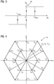
- FIG. 4 shows a space vector diagram 41 according to FIG Figures 1 and 2 executed three-level inverter 1 in a stator-fixed coordinate system with coordinates a, ⁇ .
- the space vector diagram 41 has 27 space vectors U 0 to U 26 .
- Each space vector U 0 to U 26 represents a switching state of the three-level inverter 1 in a known manner, which results from the phase switching states of the switches S U , S V , S W of the three phases U, V, W.
- a switching state of the three-level inverter 1 is denoted below by a 3-tuple (a, b, c), where a denotes the phase-switched state of the first switch S U , b denotes the phase-switched state of the second switch S V and c denotes the phase-switched state of the third switch S W denotes.
- A, b, c each take on one of the values 1, 0, -1, where the value 1 stands for the first phase switching state of the respective switch S U , S V , S W , the value 0 for the second phase switching state of the respective switch S U , S V , S W stands and the value -1 stands for the third phase switching state of the respective switch S U , S V , S W stands.
- the space vector U 8 represents the switching state (1,0, -1), which is shown in FIG 1 is shown.
- the space vectors U 0 , U 7 and U 14 are the so-called zero-voltage space vectors, which each represent a switching state in which all three switches S U , S V , S W have the same phase state.
- the space vector U 0 represents the switching state (0,0,0)
- the space vector U 7 represents the switching state (1,1,1)
- the space vector U 14 represents the switching state (-1, -1, -1).
- the zero-voltage space vectors are represented by the coordinate origin of the space vector diagram 41.
- the zero-voltage space vectors form an example of so-called redundant space vectors U 0 , U 7 , U 14 to U 26 , which coincide in the space vector diagram 41.
- the switching states represented by two redundant space vectors U 0 , U 7 , U 14 to U 26 are different, but generate (at least approximately) the same differences between the individual phase voltages and are therefore represented by space vectors U 0 , U 7 , U 14 that coincide in space vector diagram 41 to U 26 . Since the switching states of two redundant space vectors U 0 , U 7 , U 14 to U 26 generate (at least approximately) the same differences between the individual phase voltages, they also have (at least approximately) the same effect on an AC voltage side connected to the three-level inverter 1 Load.
- the space vector pairs (U 15 , U 21 ), (U 16 , U 22 ), (U 17 , U 23 ), (U 18 , U 24 ), (U 19 , U 25 ) and (U 20 , U 26 ) a pair of redundant space vectors U 15 to U 26 .
- phase currents i U , i V , i W are controlled with the current control unit 37 with a direct hysteresis current control based on several space vectors U 0 to U 26 forming a space vector group. Which space vector group is selected for regulating the phase currents i U , i V , i W depends on the actual values of the phase currents i U , i V , i W and on the hysteresis signal S as well as on the nominal output voltage of the three-level inverter 1.
- the midpoint voltage U m is also regulated, so that the midpoint voltage U m is defined by the hysteresis diagram 39 Hysteresis window for the midpoint voltage U m is returned when it leaves it.
- a different space vector group than the previously used space vector group from mutually redundant space vector groups is selected to control the phase currents i U , i V , i W in order to return the midpoint voltage U m to the hysteresis window.
- Space vector groups that are redundant to one another are referred to here as space vector groups which differ from one another only in terms of different redundant space vectors U 0 , U 7 , U 14 to U 26 .
- the regulation takes advantage of the fact that two redundant space vectors U 0 , U 7 , U 14 to U 26 represent switching states that generate (at least approximately) the same differences between the individual phase voltages, but have different effects on the midpoint voltage U m , so that the Midpoint voltage U m can be changed by changing from a space vector group previously used for regulation to a space vector group redundant for this purpose.
- that one of these criteria is preferably used which optimizes the system formed by the three-level inverter 1 and a load connected to it.
- phase currents i U , i V , i W and the midpoint voltage U m in more detail, it is assumed in the following that a space vector group is used to regulate the phase currents i U , i V , i W , which four of the space vectors U 0 to U 26 are formed, which span a rhombus in the space vector diagram 41.
- This formation of the space vector groups is used in the SDHC current control, which according to the invention is preferably used for hysteresis current control of the phase currents i U , i V , i W.
- Such a rhombus is spanned, for example, by the four space vectors U 16 , U 23 , U 3 and U 9 , which form the space vector group (U 6 , U 23 , U 3 , U 9 ).
- the space vector groups (U 22 , U 23 , U 3 , U 9 ), (U 16 , U 17 , U 3 , U 9 ) and (U 22 , U 17 , U 3 , U 9 ) are redundant for this space vector group.
- the following table shows the switching states that are represented by the space vectors U 16 , U 22 , U 17 , U 23 , U 3 , U 9 of these mutually redundant space vector groups, and a midpoint current that flows from these switching states to the midpoint 13 of the intermediate circuit 3 is directed:
- the transition from space vector U 16 to space vector U 23 requires a change in the switching state in phase U from 1 to -1 and thus a change in the phase voltage of the phase U by the full intermediate circuit voltage U Z.
- the space vector group (U 16 , U 23 , U 3 , U 9 ) therefore does not meet the above-mentioned criterion (ii).
- the transition from the space vector U 16 to the space vector U 23 requires a switchover of all three phases U, V, W. Therefore, the space vector group (U 16 , U 23 , U 3 , U 9 ) does not meet the above-mentioned criterion (iv ).
- the space vector group (U 16 , U 23 , U 3 , U 9 ) is therefore preferably not used for control.
- the transitions between the space vectors U 22 , U 23 , U 3 , U 9 only require a total of four switching operations when going around the diamond. None of these transitions requires a phase voltage to be changed by the full intermediate circuit voltage U Z. Furthermore, all of the switching states represented by the space vectors U 22 , U 23 , U 3 , U 9 in phase W match.
- the space vector group (U 22 , U 23 , U 3 , U 9 ) is therefore preferably used for regulation.
- the transitions between the space vectors U 16 , U 17 , U 3 , U 9 require a total of six switching operations when rotating around the diamond. None of these transitions requires a phase voltage to be changed by the full intermediate circuit voltage U Z. Furthermore, all of the switching states represented by the space vectors U 16 , U 17 , U 3 , U 9 in phase V correspond.
- the space vector group (U 16 , U 17 , U 3 , U 9 ) is therefore also preferably used for regulation.
- the transitions between the space vectors U 22 , U 17 , U 3 , U 9 also require a total of six switching operations when rotating around the diamond, whereby none of these transitions require a change a phase voltage around the full intermediate circuit voltage U Z requires.
- the switching states represented by the space vectors U 22 , U 17 , U 3 , U 9 do not all agree in any phase U, V, W.
- the space vector group (U 22 , U 17 , U 3 , U 9 ) is therefore preferably not used for regulation.
- the space vector group (U 22 , U 23 , U 3 , U 9 ) or the space vector group (U 16 , U 17 , U 3 , U 9 ) is therefore preferably selected for regulating the phase currents i U , i V , i W if the Regulation takes place in the diamond corresponding to these space vector groups.
- that space vector group (U 22 , U 23 , U 3 , U 9 ) or (U 16 , U 17 , U 3 , U 9 ) is selected that best meets the respective requirements, for example the switching frequency or the zero system Fulfills.
- the phase currents i U , i V , i W are controlled with the hysteresis current control used, for example with the SDHC current control, independently of the hysteresis signal S using the selected space vector group.
- the midpoint voltage U m is not regulated, but results from the hysteresis current regulation of the phase currents i U , i V , i W.
- the space vector group previously used to regulate the phase currents i U , i V , i W is replaced by one of the space vector groups (U 16 , U 23 , U 3 , U 9 ) that are redundant for this space vector group. , (U 22 , U 23 , U 3 , U 9 ), (U 16 , U 17 , U 3 , U 9 ), (U 22 , U 17 , U 3 , U 9 ) to get the midpoint voltage U m in the hysteresis window for the midpoint voltage U m .
- the previously used space vector group is preferably replaced by one of the two preferred space vector groups (U 22 , U 23 , U 3 , U 9 ), (U 16 , U 17 , U 3 , U 9 ), provided that this results in the midpoint voltage U m in the Hysteresis window can be traced back.
- phase currents i U , i V , i W and the midpoint voltage U m in other areas of the space vector diagram 41 are regulated using redundant space vector groups which form a rhombus in the respective area of the space vector diagram 41.
Landscapes
- Engineering & Computer Science (AREA)
- Power Engineering (AREA)
- Inverter Devices (AREA)
Description
Die Erfindung betrifft ein Verfahren und eine Vorrichtung zur Regelung eines dreiphasigen Drei-Level-Wechselrichters.The invention relates to a method and a device for regulating a three-phase three-level inverter.
Unter einem Drei-Level-Wechselrichter, der auch als Dreipunktwechselrichter bezeichnet wird, wird ein Wechselrichter verstanden, der gepulste Phasenspannungen erzeugt, die jeweils drei Spannungswerte annehmen können. Dazu weist der Drei-Level-Wechselrichter für jede Phase eine Schalteinheit mit drei Phasenschaltzuständen auf, durch die die Phasenspannung der Phase jeweils auf einen der drei Spannungswerte gelegt wird.A three-level inverter, which is also referred to as a three-point inverter, is understood to mean an inverter that generates pulsed phase voltages that can each assume three voltage values. For this purpose, the three-level inverter has a switching unit with three phase switching states for each phase, through which the phase voltage of the phase is in each case set to one of the three voltage values.
Zwei der drei Spannungswerte sind durch Anschlussspannungen vorgegeben, die jeweils an einem Anschluss eines gleichspannungsseitigen Zwischenkreises des Drei-Level-Wechselrichters anliegen. Der dritte Spannungswert wird hier als Mittelpunktspannung des Drei-Level-Wechselrichters bezeichnet und liegt zwischen den beiden Anschlussspannungen. Die Mittelpunktspannung ergibt sich aus dem elektrischen Potential in einem Mittelpunkt des Zwischenkreises, der üblicherweise über Zwischenkreiskondensatoren mit den beiden Anschlüssen des Zwischenkreises verbunden ist.Two of the three voltage values are specified by connection voltages which are each applied to a connection of an intermediate circuit on the DC voltage side of the three-level inverter. The third voltage value is referred to here as the midpoint voltage of the three-level inverter and lies between the two connection voltages. The midpoint voltage results from the electrical potential in a midpoint of the intermediate circuit, which is usually connected to the two connections of the intermediate circuit via intermediate circuit capacitors.
Um die Vorteile eines Drei-Level-Wechselrichters optimal nutzen zu können und die Zwischenkreiskondensatoren nicht zu überlasten, sollte die Mittelpunktspannung der Mittelwert der beiden Anschlussspannungen des Zwischenkreises sein, damit die Differenzen der Mittelpunktspannung von den beiden Anschlussspannungen betragsmäßig gleich groß sind und an jedem Zwischenkreiskondensator dieselbe Spannung anliegt. Bestimmte Schaltzustände eines Drei-Level-Wechselrichters können den Zwischenkreis jedoch unsymmetrisch belasten und dadurch zu Abweichungen der Mittelpunktspannung von dem Mittelwert der beiden Anschlussspannungen führen.In order to be able to optimally use the advantages of a three-level inverter and not to overload the intermediate circuit capacitors, the midpoint voltage should be the mean value of the two connection voltages of the intermediate circuit, so that the differences between the midpoint voltage of the two connection voltages are the same in terms of amount and the same on each intermediate circuit capacitor Voltage is present. However, certain switching states of a three-level inverter can load the intermediate circuit asymmetrically and thus lead to deviations of the midpoint voltage from the mean value of the two connection voltages.
Der Erfindung liegt die Aufgabe zugrunde, eine verbesserte Regelung eines Drei-Level-Wechselrichters anzugeben, die insbesondere eine Regelung der Mittelpunktspannung des Drei-Level-Wechselrichters umfasst.The invention is based on the object of specifying an improved regulation of a three-level inverter, which in particular comprises regulation of the midpoint voltage of the three-level inverter.
Die Aufgabe wird erfindungsgemäß durch die Merkmale des Anspruchs 1 gelöst.The object is achieved according to the invention by the features of
Vorteilhafte Ausgestaltungen der Erfindung sind Gegenstand der Unteransprüche.Advantageous embodiments of the invention are the subject of the subclaims.
Bei einem erfindungsgemäßen Verfahren zur Regelung eines dreiphasigen Drei-Level-Wechselrichters werden Phasenströme des Drei-Level-Wechselrichters mit einer direkten Hysteresestromregelung anhand von mehreren, eine Raumzeigergruppe bildenden Raumzeigern geregelt. Ferner wird eine Mittelpunktspannung eines gleichspannungsseitigen Zwischenkreises des Drei-Level-Wechselrichters geregelt, indem die zur Regelung der Phasenströme verwendete Raumzeigergruppe aus mehreren zueinander redundanten Raumzeigergruppen in Abhängigkeit von der Mittelpunktspannung ausgewählt wird.In a method according to the invention for regulating a three-phase three-level inverter, phase currents of the three-level inverter are regulated with direct hysteresis current regulation using several space vectors forming a space vector group. Furthermore, a midpoint voltage of an intermediate circuit on the DC voltage side of the three-level inverter is regulated by selecting the space vector group used to control the phase currents from several mutually redundant space vector groups depending on the midpoint voltage.
Unter einem Raumzeiger wird hier ein Vektor in einem Raumzeigerdiagramm verstanden, der eine relative Größe und Phasenlage der Phasenspannungen des Drei-Level-Wechselrichters darstellt. Als zueinander redundante Raumzeigergruppen werden Raumzeigergruppen bezeichnet, die sich voneinander nur durch redundante Raumzeiger unterscheiden. Redundante Raumzeiger repräsentierten verschiedene Schaltzustände eines Drei-Level-Wechselrichters, die (zumindest annähernd) dieselben Differenzen zwischen den einzelnen Phasenspannungen des Drei-Level-Wechselrichters erzeugen und daher auch (zumindest annähernd) dieselbe Wirkung auf eine an den Drei-Level-Wechselrichter wechselspannungsseitig angeschlossene Last haben. Redundante Raumzeiger liegen in dem Raumzeigerdiagramm aufeinander.A space vector is understood here to be a vector in a space vector diagram which represents a relative size and phase position of the phase voltages of the three-level inverter. Space vector groups that differ from one another only in terms of redundant space vector are designated as mutually redundant space vector groups. Redundant space vectors represent different switching states of a three-level inverter, which (at least approximately) the same differences between the individual phase voltages of the three-level inverter and therefore also have (at least approximately) the same effect on a load connected to the three-level inverter on the AC side. Redundant space vectors are superimposed in the space vector diagram.
Unter einer Hystereseregelung wird eine Regelung verstanden, bei der die Regelgröße in einem Toleranzbereich um einen Sollwert gehalten wird. Der Toleranzbereich wird im Folgenden als Hysteresefenster bezeichnet.A hysteresis control is understood to mean a control in which the controlled variable is kept within a tolerance range around a target value. The tolerance range is referred to below as the hysteresis window.
Unter einer direkten Stromregelung wird eine Stromregelung verstanden, bei der ein Pulsmuster für die gepulsten Phasenspannungen direkt aus einem Stromfehler abgeleitet wird. Demgegenüber wird bei einer indirekten Stromregelung zunächst ein Spannungssollwert ermittelt und anhand dieses Spannungswertes wird das Pulsmuster bestimmt.Direct current regulation is understood to mean current regulation in which a pulse pattern for the pulsed phase voltages is derived directly from a current error. In contrast, in the case of indirect current regulation, a nominal voltage value is first determined and the pulse pattern is determined on the basis of this voltage value.
Die Erfindung kombiniert eine direkte Hysteresestromregelung der Phasenströme eines Drei-Level-Wechselrichters mit einer Regelung einer Mittelpunktspannung des Drei-Level-Wechselrichters.The invention combines direct hysteresis current regulation of the phase currents of a three-level inverter with regulation of a midpoint voltage of the three-level inverter.
Verglichen mit einer auf Pulsweitenmodulation basierenden indirekten Stromregelung ermöglicht eine direkte Hysteresestromregelung der Phasenströme vorteilhaft eine höhere Dynamik und Robustheit, beispielsweise gegenüber Änderungen von Parametern der Regelstrecke, da bei einer auf Pulsweitenmodulation basierenden indirekten Stromregelung die innerhalb der Pulsperioden verwendeten Pulsmuster der Pulsweitenmodulation vorausberechnet werden müssen.Compared with an indirect current control based on pulse width modulation, direct hysteresis current control of the phase currents advantageously enables greater dynamics and robustness, for example with regard to changes in parameters of the controlled system, since with an indirect current control based on pulse width modulation the pulse patterns of the pulse width modulation used within the pulse periods must be calculated in advance.
Die Erfindung ermöglicht darüber hinaus, diese Vorteile einer direkten Hysteresestromregelung der Phasenströme mit den Vorteilen eines Drei-Level-Wechselrichters optimal nutzen zu können, indem auch die Mittelpunktspannung des Drei-Level-Wechselrichters geregelt wird.The invention also enables these advantages of direct hysteresis current regulation of the phase currents to be optimally used with the advantages of a three-level inverter, in that the midpoint voltage of the three-level inverter is also regulated.
Die Erfindung nutzt aus, dass redundante Raumzeiger zwar Schaltzustände repräsentieren, die (zumindest annähernd) dieselben Differenzen zwischen den einzelnen Phasenspannungen erzeugen, jedoch unterschiedliche Auswirkungen auf die Mittelpunktspannung haben, so dass die Mittelpunktspannung durch den Wechsel von einer bisher zur Regelung verwendeten Raumzeigergruppe zu einer dazu redundanten Raumzeigergruppe geändert werden kann.The invention takes advantage of the fact that redundant space vectors represent switching states that generate (at least approximately) the same differences between the individual phase voltages, but have different effects on the midpoint voltage, so that the midpoint voltage is generated by changing from a space vector group previously used for control to one redundant space vector group can be changed.
Eine Ausgestaltung der Erfindung sieht vor, dass zur Regelung der Mittelpunktspannung ein Hysteresefenster für die Mittelpunktspannung vorgegeben wird, und dass, wenn die Mittelpunktspannung das Hysteresefenster verlässt, eine andere Raumzeigergruppe als eine bisher verwendete Raumzeigergruppe aus den zueinander redundanten Raumzeigergruppen zur Regelung der Phasenströme ausgewählt wird, um die Mittelpunktspannung in das Hysteresefenster zurückzuführen. Diese Ausgestaltung der Erfindung reduziert vorteilhaft die Anzahl von Schalthandlungen zur Regelung des Drei-Level-Wechselrichters und dadurch verursachte Schaltverluste, indem die Regelung der Phasenströme durch die Regelung der Mittelpunktspannung nur dann beeinflusst wird, wenn die Mittelpunktspannung ein vorgegebenes Hysteresefenster verlässt, sonst aber durch die Mittelpunktspannung nicht beeinflusst wird.One embodiment of the invention provides that a hysteresis window is specified for the midpoint voltage for regulating the midpoint voltage, and that, when the midpoint voltage leaves the hysteresis window, a different space vector group than a previously used space vector group is selected from the mutually redundant space vector groups for controlling the phase currents, to return the midpoint voltage to the hysteresis window. This embodiment of the invention advantageously reduces the number of switching operations to regulate the three-level inverter and the switching losses caused thereby, in that the regulation of the phase currents is only influenced by regulating the midpoint voltage when the midpoint voltage leaves a specified hysteresis window, but otherwise through the Midpoint voltage is not influenced.
Eine weitere Ausgestaltung der Erfindung sieht vor, dass die zur Regelung verwendete Raumzeigergruppe in Abhängigkeit von einer Anzahl von Schalthandlungen ausgewählt wird, die zum Ändern von Phasenspannungen des Drei-Level-Wechselrichters bei Übergängen zwischen den Raumzeigern der Raumzeigergruppe erforderlich sind. Diese Ausgestaltung der Erfindung reduziert vorteilhaft Schaltverluste durch die Schalthandlungen.Another embodiment of the invention provides that the space vector group used for regulation is selected as a function of a number of switching operations that are required to change phase voltages of the three-level inverter during transitions between the space vectors of the space vector group. This embodiment of the invention advantageously reduces switching losses due to the switching operations.
Eine weitere Ausgestaltung der Erfindung sieht vor, dass die zur Regelung verwendete Raumzeigergruppe derart ausgewählt wird, dass bei Übergängen zwischen den Raumzeigern der Raumzeigergruppe keine Änderung einer Phasenspannung des Drei-Level-Wechselrichters um eine volle Zwischenkreisspannung des Zwischenkreises erforderlich ist. Durch diese Ausgestaltung der Erfindung werden vorteilhaft hohe Spannungsänderungen an einer mit dem Drei-Level-Wechselrichter verbundenen Last bei Schalthandlungen vermieden.Another embodiment of the invention provides that the space vector group used for regulation is selected in such a way that there is no change in a phase voltage of the three-level inverter during transitions between the space vectors of the space vector group around a full intermediate circuit voltage of the intermediate circuit is required. This embodiment of the invention advantageously avoids high voltage changes on a load connected to the three-level inverter during switching operations.
Eine weitere Ausgestaltung der Erfindung sieht vor, dass die zur Regelung verwendete Raumzeigergruppe derart ausgewählt wird, dass alle von den Raumzeigern der Raumzeigergruppe repräsentierten Schaltzustände in einer Phase des Drei-Level-Wechselrichters übereinstimmen. Durch diese Ausgestaltung der Erfindung kann ein so genanntes Flat-Top-Verhalten der Regelung erreicht werden, bei dem eine Phase während jeder Taktperiode der Regelung nicht geschaltet wird. Auch dadurch werden vorteilhaft Schaltverluste durch die Schalthandlungen reduziert.Another embodiment of the invention provides that the space vector group used for regulation is selected in such a way that all switching states represented by the space vectors of the space vector group coincide in a phase of the three-level inverter. This embodiment of the invention makes it possible to achieve what is known as a flat-top behavior of the regulation, in which a phase is not switched during each clock period of the regulation. This also advantageously reduces switching losses caused by the switching operations.
Eine weitere Ausgestaltung der Erfindung sieht vor, dass die zur Regelung verwendete Raumzeigergruppe in Abhängigkeit von einem gewünschten Nullsystemverlauf ausgewählt wird. Durch diese Ausgestaltung der Erfindung kann vorteilhaft das Nullsystem durch die Auswahl der Raumzeigergruppe an die jeweiligen anwendungsabhängigen Anforderungen angepasst werden, beispielsweise um Spannungshübe bei Schalthandlungen, die Schaltfrequenz oder Anregungen von Systemschwingungen über parasitäre Effekte zu reduzieren.A further embodiment of the invention provides that the space vector group used for regulation is selected as a function of a desired zero system course. With this embodiment of the invention, the zero system can advantageously be adapted to the respective application-dependent requirements through the selection of the space vector group, for example to reduce voltage swings during switching operations, the switching frequency or excitations of system oscillations via parasitic effects.
Eine weitere Ausgestaltung der Erfindung sieht vor, dass als Hysteresestromregelung eine SDHC-Stromregelung verwendet wird. Unter einer so genannten SDHC-Stromregelung (SDHC = Switched Diamond Hysteresis Control) wird ein Stromregelungsverfahren verstanden, das beispielsweise in
Eine erfindungsgemäße Regelungsvorrichtung zur Regelung eines dreiphasigen Drei-Level-Wechselrichters umfasst eine Spannungsmessvorrichtung zur Erfassung einer Mittelpunktspannung des Drei-Level-Wechselrichters, eine Strommessvorrichtung zur Erfassung von Phasenströmen des Drei-Level-Wechselrichters, und einen Hystereseregler mit einer Stromregelungseinheit zur direkten Hysteresestromregelung der Phasenströme anhand von mehreren eine Raumzeigergruppe bildenden Raumzeigern, wobei die Stromregelungseinheit die Raumzeigergruppe in Abhängigkeit von den erfassten Phasenströmen und von der erfassten Mittelpunktspannung auswählt. Durch eine derartige Regelungsvorrichtung kann das erfindungsgemäße Verfahren zur Regelung eines dreiphasigen Drei-Level-Wechselrichters realisiert werden. Die Vorteile einer derartigen Regelungsvorrichtung entsprechen daher den oben genannten Vorteilen des erfindungsgemäßen Verfahrens.A control device according to the invention for controlling a three-phase three-level inverter comprises a voltage measuring device for detecting a midpoint voltage of the three-level inverter, a current measuring device for detecting phase currents of the three-level inverter, and a hysteresis controller with a current control unit for direct hysteresis current control of the phase currents on the basis of several space vectors forming a space vector group, the current control unit selecting the space vector group as a function of the detected phase currents and of the detected midpoint voltage. The method according to the invention for regulating a three-phase three-level inverter can be implemented by means of such a control device. The advantages of such a control device therefore correspond to the above-mentioned advantages of the method according to the invention.
Eine Ausgestaltung der Regelungsvorrichtung sieht vor, dass der Hystereseregler ein Hystereseglied zur Erzeugung eines Hysteresesignals für die erfasste Mittelpunktspannung aufweist, wobei das Hysteresesignal signalisiert, ob die erfasste Mittelpunktspannung ein vorgegebenes Hysteresefenster für die Mittelpunktspannung verlässt.One embodiment of the control device provides that the hysteresis regulator has a hysteresis element for generating a hysteresis signal for the detected midpoint voltage, the hysteresis signal signaling whether the detected midpoint voltage leaves a predetermined hysteresis window for the midpoint voltage.
Eine weitere Ausgestaltung der Regelungsvorrichtung sieht vor, dass die Stromregelungseinheit eine andere Raumzeigergruppe als eine bisher verwendete Raumzeigergruppe aus zueinander redundanten Raumzeigergruppen zur Regelung der Phasenströme auswählt, um die Mittelpunktspannung in das Hysteresefenster zurückzuführen, wenn die Mittelpunktspannung das Hysteresefenster verlässt.Another embodiment of the control device provides that the current control unit selects a different space vector group than a previously used space vector group from mutually redundant space vector groups to control the phase currents, in order to return the midpoint voltage to the hysteresis window when the midpoint voltage leaves the hysteresis window.
Die vorgenannten Ausgestaltungen der Regelungsvorrichtung entsprechen oben genannten Ausgestaltungen des erfindungsgemäßen Verfahrens und weisen diesen Ausgestaltungen des erfindungsgemäßen Verfahrens entsprechende oben genannte Vorteile auf.The aforementioned configurations of the control device correspond to the aforementioned configurations of the method according to the invention and have the above-mentioned advantages corresponding to these configurations of the method according to the invention.
Die oben beschriebenen Eigenschaften, Merkmale und Vorteile dieser Erfindung sowie die Art und Weise, wie diese erreicht werden, werden klarer und deutlicher verständlich im Zusammenhang mit der folgenden Beschreibung von Ausführungsbeispielen, die im Zusammenhang mit den Zeichnungen näher erläutert werden. Dabei zeigen:
- FIG 1
- ein Ersatzschaltbild eines Drei-Level-Wechselrichters,
- FIG 2
- einen Schaltplan eines Ausführungsbeispiels eines Drei-Level-Wechselrichters und einer Regelungsvorrichtung zur Regelung von Phasenströmen des DreiLevel-Wechselrichters,
- FIG 3
- ein Hysteresediagramm für ein Hysteresesignal zur Regelung einer Mittelpunktspannung eines Drei-LevelWechselrichters, und
- FIG 4
- ein Raumzeigerdiagramm eines Drei-Level-Wechselrichters.
- FIG 1
- an equivalent circuit diagram of a three-level inverter,
- FIG 2
- a circuit diagram of an embodiment of a three-level inverter and a control device for regulating phase currents of the three-level inverter,
- FIG 3
- a hysteresis diagram for a hysteresis signal for regulating a midpoint voltage of a three-level inverter, and
- FIG 4
- a space vector diagram of a three-level inverter.
Einander entsprechende Teile sind in den Figuren mit denselben Bezugszeichen versehen.Corresponding parts are provided with the same reference symbols in the figures.
Der Drei-Level-Wechselrichter 1 weist gleichspannungsseitig einen Zwischenkreis 3 auf. Der Zwischenkreis 3 weist einen ersten Anschluss 5, auf den ein erstes Zwischenkreispotential Z+ gelegt wird, und einen zweiten Anschluss 7, auf den ein zweites Zwischenkreispotential Z- gelegt wird, auf. Die Differenz der Zwischenkreispotentiale Z+, Z- ist eine Zwischenkreisspannung UZ des Zwischenkreises 3. Die Anschlüsse 5, 7 sind jeweils über wenigstens einen Zwischenkreiskondensator 9, 11 mit einem Mittelpunkt 13 des Zwischenkreises 3 verbunden. Die Differenz eines Mittelpunktpotentials Zm an dem Mittelpunkt 13 und des zweiten Zwischenkreispotentials Z- wird im Folgenden als Mittelpunktspannung Um des Zwischenkreises 3 und des Drei-Level-Wechselrichters 1 bezeichnet.The three-
Ferner weist der Drei-Level-Wechselrichter 1 für jede seiner Phasen U, V, W einen Schalter SU, SV, SW mit drei Phasenschaltzuständen auf. In einem ersten Phasenschaltzustand liegt die jeweilige Phase U, V, W auf dem ersten Zwischenkreispotential Z+, in einem zweiten Phasenschaltzustand liegt die Phase U, V, W auf dem Mittelpunktpotential Zm und in dem dritten Phasenschaltzustand liegt die Phase U, V, W auf dem zweiten Zwischenkreispotential Z-. In
Wechselspannungsseitig weist der Drei-Level-Wechselrichter 1 für jede Phase U, V, W eine Anschlussklemme L1, L2, L3 auf. Zwischen dem Schalter SU, SV, SW und der Anschlussklemme L1, L2, L3 einer Phase U, V, W fließt ein Phasenstrom iU, iV, iW der Phase U, V, W. Optional weist der Drei-Level-Wechselrichter 1 einen Filter 15 auf, der für jede Phase U, V, W wenigstens eine Induktivität 17 aufweist.On the AC voltage side, the three-
Jeder Schalter SU, SV, SW wird in bekannter Weise durch eine Halbbrücke 21 mit zwei Halbbrückenzweigen 23 gebildet, die jeweils zwei Schaltglieder 25 aufweisen und über zwei Kopplungsdioden 27, deren Verbindung auf dem Mittelpunktpotential Zm liegt, miteinander verbunden sind. Jedes Schaltglied 25 weist beispielsweise einen Bipolartransistor mit isolierter Gate-Elektrode (IGBT = Insulated-Gate Bipolar Transistor) und eine dazu antiparallel geschaltete Diode auf.Each switch S U , S V , S W is formed in a known manner by a half-
Die Regelungsvorrichtung 19 umfasst eine Strommessvorrichtung 29 zur Erfassung von Istwerten der Phasenströme iU, iV, iW, eine Spannungsmessvorrichtung 31 zur Erfassung der an den Zwischenkreiskondensatoren 9 und 11 anliegenden Spannungen und einen Hystereseregler 33 zur direkten Hysteresestromregelung der Phasenströme iU, iV, iW und zur Regelung der Mittelpunktspannung Um. Der Hystereseregler 33 weist ein Hystereseglied 35 zur Erzeugung eines Hysteresesignals S für die Mittelpunktspannung Um und eine Stromregelungseinheit 37 zur Hysteresestromregelung der Phasenströme iU, iV, iW in Abhängigkeit von den erfassten Istwerten der Phasenströme iU, iV, iW und dem Hysteresesignal S auf. Die Stromregelungseinheit 37 erzeugt Schaltsignale, mit denen die Schaltglieder 25 angesteuert werden.The
Im Folgenden wird die Regelung des Drei-Level-Wechselrichters 1 anhand von
Die Raumzeiger U0, U7 und U14 sind die so genannten Nullspannungsraumzeiger, die jeweils einen Schaltzustand repräsentieren, in dem alle drei Schalter SU, SV, SW denselben Phasenzustand aufweisen. Der Raumzeiger U0 repräsentiert den Schaltzustand (0,0,0), der Raumzeiger U7 repräsentiert den Schaltzustand (1,1,1) und der Raumzeiger U14 repräsentiert den Schaltzustand (-1,-1,-1). Die Nullspannungsraumzeiger werden durch den Koordinatenursprung des Raumzeigerdiagramms 41 dargestellt.The space vectors U 0 , U 7 and U 14 are the so-called zero-voltage space vectors, which each represent a switching state in which all three switches S U , S V , S W have the same phase state. The space vector U 0 represents the switching state (0,0,0), the space vector U 7 represents the switching state (1,1,1) and the space vector U 14 represents the switching state (-1, -1, -1). The zero-voltage space vectors are represented by the coordinate origin of the space vector diagram 41.
Die Nullspannungsraumzeiger bilden ein Beispiel so genannter redundanter Raumzeiger U0, U7, U14 bis U26, die im Raumzeigerdiagramm 41 zusammenfallen. Die von zwei redundanten Raumzeigern U0, U7, U14 bis U26 repräsentierten Schaltzustände sind verschieden, erzeugen jedoch (zumindest annähernd) dieselben Differenzen zwischen den einzelnen Phasenspannungen und werden deshalb durch im Raumzeigerdiagramm 41 zusammenfallende Raumzeiger U0, U7, U14 bis U26 repräsentiert. Da die Schaltzustände zweier redundanter Raumzeiger U0, U7, U14 bis U26 (zumindest annähernd) dieselben Differenzen zwischen den einzelnen Phasenspannungen erzeugen, haben sie auch (zumindest annähernd) dieselbe Wirkung auf eine an den Drei-Level-Wechselrichter 1 wechselspannungsseitig angeschlossene Last. Neben den Nullspannungsraumzeigern bilden die Raumzeigerpaare (U15, U21), (U16, U22), (U17, U23), (U18, U24), (U19, U25) und (U20, U26) jeweils ein Paar redundanter Raumzeiger U15 bis U26.The zero-voltage space vectors form an example of so-called redundant space vectors U 0 , U 7 , U 14 to U 26 , which coincide in the space vector diagram 41. The switching states represented by two redundant space vectors U 0 , U 7 , U 14 to U 26 are different, but generate (at least approximately) the same differences between the individual phase voltages and are therefore represented by space vectors U 0 , U 7 , U 14 that coincide in space vector diagram 41 to U 26 . Since the switching states of two redundant space vectors U 0 , U 7 , U 14 to U 26 generate (at least approximately) the same differences between the individual phase voltages, they also have (at least approximately) the same effect on an AC voltage side connected to the three-
Die Phasenströme iU, iV, iW werden mit der Stromregelungseinheit 37 mit einer direkten Hysteresestromregelung anhand von mehreren, eine Raumzeigergruppe bildenden Raumzeigern U0 bis U26 geregelt. Welche Raumzeigergruppe zur Regelung der Phasenströme iU, iV, iW jeweils ausgewählt wird, hängt von den Istwerten der Phasenströme iU, iV, iW und von dem Hysteresesignal S sowie von der Sollausgangsspannung des Drei-Level-Wechselrichters 1 ab. Dabei wird durch die Auswahl der Raumzeigergruppe in Abhängigkeit von dem Hysteresesignal S auch die Mittelpunktspannung Um geregelt, so dass die Mittelpunktspannung Um in das durch das Hysteresediagramm 39 definierte Hysteresefenster für die Mittelpunktspannung Um zurückgeführt wird, wenn sie es verlässt. Dazu wird, wenn die Mittelpunktspannung Um das Hysteresefenster verlässt, eine andere Raumzeigergruppe als die bisher verwendete Raumzeigergruppe aus zueinander redundanten Raumzeigergruppen zur Regelung der Phasenströme iU, iV, iW ausgewählt, um die Mittelpunktspannung Um in das Hysteresefenster zurückzuführen. Als zueinander redundante Raumzeigergruppen werden dabei Raumzeigergruppen bezeichnet, die sich voneinander nur durch verschiedene redundante Raumzeiger U0, U7, U14 bis U26 unterscheiden.The phase currents i U , i V , i W are controlled with the
Die Regelung nutzt aus, dass zwei redundante Raumzeiger U0, U7, U14 bis U26 zwar Schaltzustände repräsentieren, die (zumindest annähernd) dieselben Differenzen zwischen den einzelnen Phasenspannungen erzeugen, jedoch unterschiedliche Auswirkungen auf die Mittelpunktspannung Um haben, so dass die Mittelpunktspannung Um durch den Wechsel von einer bisher zur Regelung verwendeten Raumzeigergruppe zu einer dazu redundanten Raumzeigergruppe geändert werden kann.The regulation takes advantage of the fact that two redundant space vectors U 0 , U 7 , U 14 to U 26 represent switching states that generate (at least approximately) the same differences between the individual phase voltages, but have different effects on the midpoint voltage U m , so that the Midpoint voltage U m can be changed by changing from a space vector group previously used for regulation to a space vector group redundant for this purpose.
Zur Optimierung der Regelung wird die zur Regelung verwendete Raumzeigergruppe ferner vorzugsweise derart ausgewählt, dass sie wenigstens eines der folgenden Kriterien (i) bis (iv) erfüllt:
- (i) Die Übergänge zwischen den Raumzeigern U0 bis U26 der Raumzeigergruppe erfordern möglichst wenige Schalthandlungen zum Umschalten der Phasenspannungen des Drei-Level-
Wechselrichter 1. Dadurch werden vorteilhaft Schaltverluste durch die Schalthandlungen reduziert. - (ii) Die Übergänge zwischen den Raumzeigern U0 bis U26 der Raumzeigergruppe erfordern keine Änderung einer Phasenspannung um die volle Zwischenkreisspannung UZ. Dadurch werden vorteilhaft hohe Spannungssprünge an einer mit dem Drei-Level-
Wechselrichter 1 verbundenen Last vermieden. - (iii) Die Raumzeigergruppe erzeugt möglichst geringe Sprünge im gebildeten Nullsystem. Dadurch werden vorteilhaft Anregungen von Systemschwingungen über parasitäre Effekte und Spannungsbelastungen durch Sprünge im Nullsystem reduziert.
- (iv) Alle von den Raumzeigern U0 bis U26 der Raumzeigergruppe repräsentierten Schaltzustände stimmen in einer Phase überein. Dadurch kann ein so genanntes Flat-Top-Verhalten der Regelung erreicht werden, bei dem eine Phase während jeder Taktperiode der Regelung nicht geschaltet wird. Auch dadurch werden vorteilhaft Schaltverluste durch die Schalthandlungen reduziert.
- (i) The transitions between the space vectors U 0 to U 26 of the space vector group require as few switching operations as possible to switch the phase voltages of the three-
level inverter 1. This advantageously reduces switching losses due to the switching operations. - (ii) The transitions between the space vectors U 0 to U 26 of the space vector group do not require a phase voltage to be changed by the full intermediate circuit voltage U Z. This advantageously avoids high voltage jumps on a load connected to the three-
level inverter 1. - (iii) The space vector group generates the smallest possible jumps in the zero system. This advantageously reduces excitations of system oscillations via parasitic effects and voltage loads due to jumps in the zero system.
- (iv) All switching states represented by the space vectors U 0 to U 26 of the space vector group coincide in one phase. This enables a so-called flat-top behavior of the control to be achieved, in which a phase is not switched during each control cycle period. This also advantageously reduces switching losses caused by the switching operations.
Vorzugsweise wird dasjenige dieser Kriterien bevorzugt verwendet, welches das von dem Drei-Level-Wechselrichter 1 und einer mit ihm verbundenen Last gebildete System optimiert.Preferably, that one of these criteria is preferably used which optimizes the system formed by the three-
Um die oben beschriebene Regelung der Phasenströme iU, iV, iW und der Mittelpunktspannung Um eingehender zu erläutern, wird im Folgenden davon ausgegangen, dass zur Regelung der Phasenströme iU, iV, iW jeweils eine Raumzeigergruppe verwendet wird, die von vier der Raumzeiger U0 bis U26 gebildet wird, die im Raumzeigerdiagramm 41 eine Raute aufspannen. Diese Bildung der Raumzeigergruppen wird in der SDHC-Stromregelung verwendet, die erfindungsgemäß bevorzugt zur Hysteresestromregelung der Phasenströme iU, iV, iW verwendet wird.In order to explain the above-described regulation of the phase currents i U , i V , i W and the midpoint voltage U m in more detail, it is assumed in the following that a space vector group is used to regulate the phase currents i U , i V , i W , which four of the space vectors U 0 to U 26 are formed, which span a rhombus in the space vector diagram 41. This formation of the space vector groups is used in the SDHC current control, which according to the invention is preferably used for hysteresis current control of the phase currents i U , i V , i W.
Eine derartige Raute wird beispielsweise durch die vier Raumzeiger U16, U23, U3 und U9 aufgespannt, die die Raumzeigergruppe (U6, U23, U3, U9) bilden. Zu dieser Raumzeigergruppe sind die Raumzeigergruppen (U22, U23, U3, U9), (U16, U17, U3, U9) und (U22, U17, U3, U9) redundant. Die folgende Tabelle zeigt die Schaltzustände, die von den Raumzeigern U16, U22, U17, U23, U3, U9 dieser zueinander redundanten Raumzeigergruppen repräsentiert werden, und einen Mittelpunktstrom, der von diesen Schaltzuständen jeweils auf den Mittelpunkt 13 des Zwischenkreises 3 geleitet wird:
Bei der Raumzeigergruppe (U16, U23, U3, U9) erfordert der Übergang von dem Raumzeiger U16 zu dem Raumzeiger U23 eine Änderung des Schaltzustands in der Phase U von 1 auf -1 und damit eine Änderung der Phasenspannung der Phase U um die volle Zwischenkreisspannung UZ. Daher erfüllt die Raumzeigergruppe (U16, U23, U3, U9) nicht das oben genannte Kriterium (ii). Überdies erfordert der Übergang von dem Raumzeiger U16 zu dem Raumzeiger U23 eine Umschaltung aller drei Phasen U, V, W. Daher erfüllt die Raumzeigergruppe (U16, U23, U3, U9) auch nicht das oben genannte Kriterium (iv). Deshalb wird die Raumzeigergruppe (U16, U23, U3, U9) vorzugsweise nicht zur Regelung verwendet.In the case of the space vector group (U 16 , U 23 , U 3 , U 9 ), the transition from space vector U 16 to space vector U 23 requires a change in the switching state in phase U from 1 to -1 and thus a change in the phase voltage of the phase U by the full intermediate circuit voltage U Z. The space vector group (U 16 , U 23 , U 3 , U 9 ) therefore does not meet the above-mentioned criterion (ii). In addition, the transition from the space vector U 16 to the space vector U 23 requires a switchover of all three phases U, V, W. Therefore, the space vector group (U 16 , U 23 , U 3 , U 9 ) does not meet the above-mentioned criterion (iv ). The space vector group (U 16 , U 23 , U 3 , U 9 ) is therefore preferably not used for control.
Bei der Raumzeigergruppe (U22, U23, U3, U9) erfordern die Übergänge zwischen den Raumzeigern U22, U23, U3, U9 bei einem Umlauf um die Raute nur insgesamt vier Schalthandlungen. Keiner dieser Übergänge erfordert eine Änderung einer Phasenspannung um die volle Zwischenkreisspannung UZ. Ferner stimmen alle von den Raumzeigern U22, U23, U3, U9 repräsentierten Schaltzustände in der Phase W überein. Die Raumzeigergruppe (U22, U23, U3, U9) wird daher bevorzugt zur Regelung verwendet.In the case of the space vector group (U 22 , U 23 , U 3 , U 9 ), the transitions between the space vectors U 22 , U 23 , U 3 , U 9 only require a total of four switching operations when going around the diamond. None of these transitions requires a phase voltage to be changed by the full intermediate circuit voltage U Z. Furthermore, all of the switching states represented by the space vectors U 22 , U 23 , U 3 , U 9 in phase W match. The space vector group (U 22 , U 23 , U 3 , U 9 ) is therefore preferably used for regulation.
Bei der Raumzeigergruppe (U16, U17, U3, U9) erfordern die Übergänge zwischen den Raumzeigern U16, U17, U3, U9 bei einem Umlauf um die Raute insgesamt sechs Schalthandlungen. Keiner dieser Übergänge erfordert eine Änderung einer Phasenspannung um die volle Zwischenkreisspannung UZ. Ferner stimmen alle von den Raumzeigern U16, U17, U3, U9 repräsentierten Schaltzustände in der Phase V überein. Die Raumzeigergruppe (U16, U17, U3, U9) wird daher ebenfalls bevorzugt zur Regelung verwendet.In the case of the space vector group (U 16 , U 17 , U 3 , U 9 ), the transitions between the space vectors U 16 , U 17 , U 3 , U 9 require a total of six switching operations when rotating around the diamond. None of these transitions requires a phase voltage to be changed by the full intermediate circuit voltage U Z. Furthermore, all of the switching states represented by the space vectors U 16 , U 17 , U 3 , U 9 in phase V correspond. The space vector group (U 16 , U 17 , U 3 , U 9 ) is therefore also preferably used for regulation.
Bei der Raumzeigergruppe (U22, U17, U3, U9) erfordern die Übergänge zwischen den Raumzeigern U22, U17, U3, U9 bei einem Umlauf um die Raute ebenfalls insgesamt sechs Schalthandlungen, wobei keiner dieser Übergänge eine Änderung einer Phasenspannung um die volle Zwischenkreisspannung UZ erfordert. Allerdings stimmen die von den Raumzeigern U22, U17, U3, U9 repräsentierten Schaltzustände in keiner Phase U, V, W sämtlich überein. Daher wird die Raumzeigergruppe (U22, U17, U3, U9) vorzugsweise nicht zur Regelung verwendet.In the case of the space vector group (U 22 , U 17 , U 3 , U 9 ), the transitions between the space vectors U 22 , U 17 , U 3 , U 9 also require a total of six switching operations when rotating around the diamond, whereby none of these transitions require a change a phase voltage around the full intermediate circuit voltage U Z requires. However, the switching states represented by the space vectors U 22 , U 17 , U 3 , U 9 do not all agree in any phase U, V, W. The space vector group (U 22 , U 17 , U 3 , U 9 ) is therefore preferably not used for regulation.
Vorzugsweise wird daher die Raumzeigergruppe (U22, U23, U3, U9) oder die Raumzeigergruppe (U16, U17, U3, U9) zur Regelung der Phasenströme iU, iV, iW ausgewählt, wenn die Regelung in der diesen Raumzeigergruppen entsprechenden Raute erfolgt. Je nach Anwendung wird diejenige Raumzeigergruppe (U22, U23, U3, U9) oder (U16, U17, U3, U9) ausgewählt, die die jeweiligen Anforderungen, beispielsweise an die Schaltfrequenz oder das Nullsystem, am besten erfüllt. Solange das Hysteresesignal S den Wert 0 annimmt, werden die Phasenströme iU, iV, iW mit der verwendeten Hysteresestromregelung, beispielsweise mit der SDHC-Stromregelung, unabhängig von dem Hysteresesignal S anhand der jeweils ausgewählten Raumzeigergruppe geregelt. Die Mittelpunktspannung Um wird dabei nicht geregelt, sondern ergibt sich dabei aus der Hysteresestromregelung der Phasenströme iU, iV, iW. Wenn das Hysteresesignal S den Wert 1 oder -1 annimmt, wird die bisher zur Regelung der Phasenströme iU, iV, iW verwendete Raumzeigergruppe durch eine der zu dieser Raumzeigergruppe redundanten Raumzeigergruppen (U16, U23, U3, U9), (U22, U23, U3, U9), (U16, U17, U3, U9), (U22, U17, U3, U9) ersetzt, um die Mittelpunktspannung Um in das Hysteresefenster für die Mittelpunktspannung Um zurückzuführen. Dabei wird die bisher verwendete Raumzeigergruppe vorzugsweise durch eine der beiden bevorzugten Raumzeigergruppen (U22, U23, U3, U9), (U16, U17, U3, U9) ersetzt, sofern dadurch die Mittelpunktspannung Um in das Hysteresefenster zurückgeführt werden kann.The space vector group (U 22 , U 23 , U 3 , U 9 ) or the space vector group (U 16 , U 17 , U 3 , U 9 ) is therefore preferably selected for regulating the phase currents i U , i V , i W if the Regulation takes place in the diamond corresponding to these space vector groups. Depending on the application, that space vector group (U 22 , U 23 , U 3 , U 9 ) or (U 16 , U 17 , U 3 , U 9 ) is selected that best meets the respective requirements, for example the switching frequency or the zero system Fulfills. As long as the hysteresis signal S assumes the value 0, the phase currents i U , i V , i W are controlled with the hysteresis current control used, for example with the SDHC current control, independently of the hysteresis signal S using the selected space vector group. The midpoint voltage U m is not regulated, but results from the hysteresis current regulation of the phase currents i U , i V , i W. If the hysteresis signal S assumes the
Entsprechend werden die Phasenströme iU, iV, iW und die Mittelpunktspannung Um in anderen Bereichen des Raumzeigerdiagramms 41 anhand von redundanten Raumzeigergruppen geregelt, die in dem jeweiligen Bereich des Raumzeigerdiagramms 41 eine Raute bilden.Correspondingly, the phase currents i U , i V , i W and the midpoint voltage U m in other areas of the space vector diagram 41 are regulated using redundant space vector groups which form a rhombus in the respective area of the space vector diagram 41.
Obwohl die Erfindung im Detail durch bevorzugte Ausführungsbeispiele näher illustriert und beschrieben wurde, so ist die Erfindung nicht durch die offenbarten Beispiele eingeschränkt und andere Variationen können vom Fachmann hieraus abgeleitet werden, ohne den Schutzumfang der Ansprüche zu verlassen.Although the invention has been illustrated and described in greater detail by preferred exemplary embodiments, the invention is not restricted by the disclosed examples and other variations can be derived from them by the person skilled in the art without departing from the scope of protection of the claims.
Claims (7)
- Method for regulating a three-phase three-level inverter (1), wherein- phase currents (iU, iV, iW) of the three-level inverter (1) are regulated with a direct hysteresis current regulation on the basis of a number of space phasors (U0 to U26) forming a space phasor group, and- a central point voltage (Um) of a DC-side intermediate circuit (3) of the three-level inverter (1) is regulated by the space phasor group used to regulate the phase currents (iU, iV, iW) being selected from a number of space phasor groups which are redundant with respect to one another as a function of the central point voltage (Um),characterised in that
in order to regulate the central point voltage (Um) a hysteresis window is predetermined for the central point voltage (Um) and if the central point voltage ((Um) leaves the hysteresis window, another space phasor group is selected as a previously used space phasor group from the space phasor groups, which are redundant with respect to one another, for regulating the phase currents (iU, iV, iW) in order to feed the central point voltage (Um) back into the hysteresis window. - Method according to one of the preceding claims, characterised in that the space phasor group used for regulation is selected as a function of a number of switching operations which are required to change from phase voltages of the three-level inverter (1) with transitions between the space phasors (U0 to U26) of the space phasor group.
- Method according to one of the preceding claims, characterised in that the space phasor group used for regulation is selected so that with transitions between the space phasors (U0 to U26) of the space phasor group, there is no need to change a phase voltage of the three level inverter (1) by a full intermediate circuit voltage (Uz) of the intermediate circuit (3).
- Method according to one of the preceding claims, characterised in that the space phasor group used for regulation is selected so that all switching states represented by the space phasors (U0 to U26) of the space phasor group match in a phase (U, V, W) of the three level inverter (1).
- Method according to one of the preceding claims, characterised in that the space phasor group used for regulation is selected as a function of a desired zero system profile.
- Method according to one of the preceding claims, characterised in that an SDHC power regulation is used as a hysteresis current regulation.
- Regulation device (19) for regulating a three-phase three-level inverter (1), the regulation device (19) comprising- a voltage measuring device (31) designed to acquire a central point voltage (Um) of the three-level inverter (1),- a current measuring device (29) designed to acquire phase currents (iU, iV, iW) of the three-level inverter (1), and- a hysteresis regulator (33) with a current regulation unit (37) for direct hysteresis current regulation of the phase currents (iU, iV, iW) on the basis of a number of space phasors (U0 to U26) forming a space phasor group, wherein the current regulation unit (37) is designed to select the space phasor group as a function of the acquired phase currents (iU, iV, iW) and of the acquired central point voltage (Um),characterised in that
the hysteresis regulator (33) has a hysteresis element (35) for generating a hysteresis signal (S) for the acquired central point voltage (Um), wherein the hysteresis signal (S) indicates whether the acquired central point voltage (Um) leaves a predetermined hysteresis window for the central point voltage (Um), and the current regulation unit (37) is designed to select another space phasor group as a previously used space phasor group from space phasor groups, which are redundant with respect to one another, for regulating the phase currents (iU, iV, iW) in order to feed the central point voltage (Um) back into the hysteresis window if the central point voltage (Um) leaves the hysteresis window.
Priority Applications (1)
| Application Number | Priority Date | Filing Date | Title |
|---|---|---|---|
| EP16190787.8A EP3300242B1 (en) | 2016-09-27 | 2016-09-27 | Regulation of a three-level inverter |
Applications Claiming Priority (1)
| Application Number | Priority Date | Filing Date | Title |
|---|---|---|---|
| EP16190787.8A EP3300242B1 (en) | 2016-09-27 | 2016-09-27 | Regulation of a three-level inverter |
Publications (2)
| Publication Number | Publication Date |
|---|---|
| EP3300242A1 EP3300242A1 (en) | 2018-03-28 |
| EP3300242B1 true EP3300242B1 (en) | 2020-10-28 |
Family
ID=57144761
Family Applications (1)
| Application Number | Title | Priority Date | Filing Date |
|---|---|---|---|
| EP16190787.8A Active EP3300242B1 (en) | 2016-09-27 | 2016-09-27 | Regulation of a three-level inverter |
Country Status (1)
| Country | Link |
|---|---|
| EP (1) | EP3300242B1 (en) |
Families Citing this family (1)
| Publication number | Priority date | Publication date | Assignee | Title |
|---|---|---|---|---|
| EP3576284A1 (en) * | 2018-05-30 | 2019-12-04 | Siemens Aktiengesellschaft | Electrical coupling of a first electrical network with a second electric network |
-
2016
- 2016-09-27 EP EP16190787.8A patent/EP3300242B1/en active Active
Non-Patent Citations (1)
| Title |
|---|
| None * |
Also Published As
| Publication number | Publication date |
|---|---|
| EP3300242A1 (en) | 2018-03-28 |
Similar Documents
| Publication | Publication Date | Title |
|---|---|---|
| EP2831989B1 (en) | Rectifier circuit with current injection | |
| DE112008001796B4 (en) | Inverter system and control method | |
| EP3245727B1 (en) | Converter module for a multi-level energy converter | |
| DE112009004353T5 (en) | Power conversion device | |
| DE102020108035B3 (en) | Modular multilevel converter, method for operating modular multilevel converters and computer program | |
| EP2144360B1 (en) | Method for operating a converter and corresponding device | |
| EP3504781B1 (en) | Hysteresis control of an output current of a power converter | |
| EP2992595A1 (en) | Converter assembly having multi-step converters connected in parallel and method for controlling said multi-step converters | |
| EP2697901B1 (en) | Voltage setting device | |
| EP4046268B1 (en) | Determination of filter parameters within an inverter | |
| AT516643B1 (en) | Rectifier circuit | |
| EP3300242B1 (en) | Regulation of a three-level inverter | |
| EP0743744B1 (en) | Current converter | |
| EP0986287A2 (en) | Two exits switching circuit,its circuit, and its control process of power delivered to the switching circuit exits | |
| DE102018124998B4 (en) | Power electronic converter and method for controlling the same | |
| EP3482488B1 (en) | Control of phase flows of inverter connected in parallel | |
| DE102021130390A1 (en) | Method and device for generating a three-phase voltage | |
| EP3476035B1 (en) | Control of phase currents of an inverter | |
| AT514654A1 (en) | Rectifier circuit with current injection | |
| EP3353885A1 (en) | Method for operating a modular multi-level power converter, modular multi-level power converter, and computer program | |
| EP3556003B1 (en) | Multi-level converter and method for operating the same | |
| DE112015000929T5 (en) | Device and method for reducing harmonics | |
| DE102022117740B3 (en) | Method for operating a hybrid multilevel converter, hybrid multilevel converter and computer program | |
| DE3907940A1 (en) | Method for symmetrising the voltage sharing in power converters having multi-point connection | |
| EP1742343A1 (en) | Modulation method |
Legal Events
| Date | Code | Title | Description |
|---|---|---|---|
| PUAI | Public reference made under article 153(3) epc to a published international application that has entered the european phase |
Free format text: ORIGINAL CODE: 0009012 |
|
| STAA | Information on the status of an ep patent application or granted ep patent |
Free format text: STATUS: THE APPLICATION HAS BEEN PUBLISHED |
|
| AK | Designated contracting states |
Kind code of ref document: A1 Designated state(s): AL AT BE BG CH CY CZ DE DK EE ES FI FR GB GR HR HU IE IS IT LI LT LU LV MC MK MT NL NO PL PT RO RS SE SI SK SM TR |
|
| AX | Request for extension of the european patent |
Extension state: BA ME |
|
| STAA | Information on the status of an ep patent application or granted ep patent |
Free format text: STATUS: REQUEST FOR EXAMINATION WAS MADE |
|
| 17P | Request for examination filed |
Effective date: 20180920 |
|
| RBV | Designated contracting states (corrected) |
Designated state(s): AL AT BE BG CH CY CZ DE DK EE ES FI FR GB GR HR HU IE IS IT LI LT LU LV MC MK MT NL NO PL PT RO RS SE SI SK SM TR |
|
| GRAP | Despatch of communication of intention to grant a patent |
Free format text: ORIGINAL CODE: EPIDOSNIGR1 |
|
| STAA | Information on the status of an ep patent application or granted ep patent |
Free format text: STATUS: GRANT OF PATENT IS INTENDED |
|
| INTG | Intention to grant announced |
Effective date: 20200622 |
|
| GRAS | Grant fee paid |
Free format text: ORIGINAL CODE: EPIDOSNIGR3 |
|
| GRAA | (expected) grant |
Free format text: ORIGINAL CODE: 0009210 |
|
| STAA | Information on the status of an ep patent application or granted ep patent |
Free format text: STATUS: THE PATENT HAS BEEN GRANTED |
|
| AK | Designated contracting states |
Kind code of ref document: B1 Designated state(s): AL AT BE BG CH CY CZ DE DK EE ES FI FR GB GR HR HU IE IS IT LI LT LU LV MC MK MT NL NO PL PT RO RS SE SI SK SM TR |
|
| REG | Reference to a national code |
Ref country code: GB Ref legal event code: FG4D Free format text: NOT ENGLISH |
|
| REG | Reference to a national code |
Ref country code: CH Ref legal event code: EP |
|
| REG | Reference to a national code |
Ref country code: DE Ref legal event code: R096 Ref document number: 502016011537 Country of ref document: DE |
|
| REG | Reference to a national code |
Ref country code: AT Ref legal event code: REF Ref document number: 1329242 Country of ref document: AT Kind code of ref document: T Effective date: 20201115 |
|
| REG | Reference to a national code |
Ref country code: IE Ref legal event code: FG4D Free format text: LANGUAGE OF EP DOCUMENT: GERMAN |
|
| REG | Reference to a national code |
Ref country code: NL Ref legal event code: MP Effective date: 20201028 |
|
| PG25 | Lapsed in a contracting state [announced via postgrant information from national office to epo] |
Ref country code: NO Free format text: LAPSE BECAUSE OF FAILURE TO SUBMIT A TRANSLATION OF THE DESCRIPTION OR TO PAY THE FEE WITHIN THE PRESCRIBED TIME-LIMIT Effective date: 20210128 Ref country code: RS Free format text: LAPSE BECAUSE OF FAILURE TO SUBMIT A TRANSLATION OF THE DESCRIPTION OR TO PAY THE FEE WITHIN THE PRESCRIBED TIME-LIMIT Effective date: 20201028 Ref country code: PT Free format text: LAPSE BECAUSE OF FAILURE TO SUBMIT A TRANSLATION OF THE DESCRIPTION OR TO PAY THE FEE WITHIN THE PRESCRIBED TIME-LIMIT Effective date: 20210301 Ref country code: GR Free format text: LAPSE BECAUSE OF FAILURE TO SUBMIT A TRANSLATION OF THE DESCRIPTION OR TO PAY THE FEE WITHIN THE PRESCRIBED TIME-LIMIT Effective date: 20210129 Ref country code: FI Free format text: LAPSE BECAUSE OF FAILURE TO SUBMIT A TRANSLATION OF THE DESCRIPTION OR TO PAY THE FEE WITHIN THE PRESCRIBED TIME-LIMIT Effective date: 20201028 |
|
| REG | Reference to a national code |
Ref country code: LT Ref legal event code: MG4D |
|
| PG25 | Lapsed in a contracting state [announced via postgrant information from national office to epo] |
Ref country code: SE Free format text: LAPSE BECAUSE OF FAILURE TO SUBMIT A TRANSLATION OF THE DESCRIPTION OR TO PAY THE FEE WITHIN THE PRESCRIBED TIME-LIMIT Effective date: 20201028 Ref country code: ES Free format text: LAPSE BECAUSE OF FAILURE TO SUBMIT A TRANSLATION OF THE DESCRIPTION OR TO PAY THE FEE WITHIN THE PRESCRIBED TIME-LIMIT Effective date: 20201028 Ref country code: PL Free format text: LAPSE BECAUSE OF FAILURE TO SUBMIT A TRANSLATION OF THE DESCRIPTION OR TO PAY THE FEE WITHIN THE PRESCRIBED TIME-LIMIT Effective date: 20201028 Ref country code: LV Free format text: LAPSE BECAUSE OF FAILURE TO SUBMIT A TRANSLATION OF THE DESCRIPTION OR TO PAY THE FEE WITHIN THE PRESCRIBED TIME-LIMIT Effective date: 20201028 Ref country code: IS Free format text: LAPSE BECAUSE OF FAILURE TO SUBMIT A TRANSLATION OF THE DESCRIPTION OR TO PAY THE FEE WITHIN THE PRESCRIBED TIME-LIMIT Effective date: 20210228 Ref country code: BG Free format text: LAPSE BECAUSE OF FAILURE TO SUBMIT A TRANSLATION OF THE DESCRIPTION OR TO PAY THE FEE WITHIN THE PRESCRIBED TIME-LIMIT Effective date: 20210128 |
|
| PG25 | Lapsed in a contracting state [announced via postgrant information from national office to epo] |
Ref country code: HR Free format text: LAPSE BECAUSE OF FAILURE TO SUBMIT A TRANSLATION OF THE DESCRIPTION OR TO PAY THE FEE WITHIN THE PRESCRIBED TIME-LIMIT Effective date: 20201028 Ref country code: NL Free format text: LAPSE BECAUSE OF FAILURE TO SUBMIT A TRANSLATION OF THE DESCRIPTION OR TO PAY THE FEE WITHIN THE PRESCRIBED TIME-LIMIT Effective date: 20201028 |
|
| REG | Reference to a national code |
Ref country code: DE Ref legal event code: R097 Ref document number: 502016011537 Country of ref document: DE |
|
| PG25 | Lapsed in a contracting state [announced via postgrant information from national office to epo] |
Ref country code: SK Free format text: LAPSE BECAUSE OF FAILURE TO SUBMIT A TRANSLATION OF THE DESCRIPTION OR TO PAY THE FEE WITHIN THE PRESCRIBED TIME-LIMIT Effective date: 20201028 Ref country code: RO Free format text: LAPSE BECAUSE OF FAILURE TO SUBMIT A TRANSLATION OF THE DESCRIPTION OR TO PAY THE FEE WITHIN THE PRESCRIBED TIME-LIMIT Effective date: 20201028 Ref country code: LT Free format text: LAPSE BECAUSE OF FAILURE TO SUBMIT A TRANSLATION OF THE DESCRIPTION OR TO PAY THE FEE WITHIN THE PRESCRIBED TIME-LIMIT Effective date: 20201028 Ref country code: SM Free format text: LAPSE BECAUSE OF FAILURE TO SUBMIT A TRANSLATION OF THE DESCRIPTION OR TO PAY THE FEE WITHIN THE PRESCRIBED TIME-LIMIT Effective date: 20201028 Ref country code: EE Free format text: LAPSE BECAUSE OF FAILURE TO SUBMIT A TRANSLATION OF THE DESCRIPTION OR TO PAY THE FEE WITHIN THE PRESCRIBED TIME-LIMIT Effective date: 20201028 Ref country code: CZ Free format text: LAPSE BECAUSE OF FAILURE TO SUBMIT A TRANSLATION OF THE DESCRIPTION OR TO PAY THE FEE WITHIN THE PRESCRIBED TIME-LIMIT Effective date: 20201028 |
|
| PG25 | Lapsed in a contracting state [announced via postgrant information from national office to epo] |
Ref country code: DK Free format text: LAPSE BECAUSE OF FAILURE TO SUBMIT A TRANSLATION OF THE DESCRIPTION OR TO PAY THE FEE WITHIN THE PRESCRIBED TIME-LIMIT Effective date: 20201028 |
|
| PLBE | No opposition filed within time limit |
Free format text: ORIGINAL CODE: 0009261 |
|
| STAA | Information on the status of an ep patent application or granted ep patent |
Free format text: STATUS: NO OPPOSITION FILED WITHIN TIME LIMIT |
|
| 26N | No opposition filed |
Effective date: 20210729 |
|
| PG25 | Lapsed in a contracting state [announced via postgrant information from national office to epo] |
Ref country code: AL Free format text: LAPSE BECAUSE OF FAILURE TO SUBMIT A TRANSLATION OF THE DESCRIPTION OR TO PAY THE FEE WITHIN THE PRESCRIBED TIME-LIMIT Effective date: 20201028 |
|
| PG25 | Lapsed in a contracting state [announced via postgrant information from national office to epo] |
Ref country code: SI Free format text: LAPSE BECAUSE OF FAILURE TO SUBMIT A TRANSLATION OF THE DESCRIPTION OR TO PAY THE FEE WITHIN THE PRESCRIBED TIME-LIMIT Effective date: 20201028 |
|
| REG | Reference to a national code |
Ref country code: CH Ref legal event code: PL |
|
| REG | Reference to a national code |
Ref country code: BE Ref legal event code: MM Effective date: 20210930 |
|
| GBPC | Gb: european patent ceased through non-payment of renewal fee |
Effective date: 20210927 |
|
| PG25 | Lapsed in a contracting state [announced via postgrant information from national office to epo] |
Ref country code: IS Free format text: LAPSE BECAUSE OF FAILURE TO SUBMIT A TRANSLATION OF THE DESCRIPTION OR TO PAY THE FEE WITHIN THE PRESCRIBED TIME-LIMIT Effective date: 20210228 Ref country code: MC Free format text: LAPSE BECAUSE OF FAILURE TO SUBMIT A TRANSLATION OF THE DESCRIPTION OR TO PAY THE FEE WITHIN THE PRESCRIBED TIME-LIMIT Effective date: 20201028 |
|
| PG25 | Lapsed in a contracting state [announced via postgrant information from national office to epo] |
Ref country code: LU Free format text: LAPSE BECAUSE OF NON-PAYMENT OF DUE FEES Effective date: 20210927 Ref country code: IE Free format text: LAPSE BECAUSE OF NON-PAYMENT OF DUE FEES Effective date: 20210927 Ref country code: GB Free format text: LAPSE BECAUSE OF NON-PAYMENT OF DUE FEES Effective date: 20210927 Ref country code: BE Free format text: LAPSE BECAUSE OF NON-PAYMENT OF DUE FEES Effective date: 20210930 |
|
| PG25 | Lapsed in a contracting state [announced via postgrant information from national office to epo] |
Ref country code: LI Free format text: LAPSE BECAUSE OF NON-PAYMENT OF DUE FEES Effective date: 20210930 Ref country code: CH Free format text: LAPSE BECAUSE OF NON-PAYMENT OF DUE FEES Effective date: 20210930 |
|
| REG | Reference to a national code |
Ref country code: AT Ref legal event code: MM01 Ref document number: 1329242 Country of ref document: AT Kind code of ref document: T Effective date: 20210927 |
|
| PG25 | Lapsed in a contracting state [announced via postgrant information from national office to epo] |
Ref country code: AT Free format text: LAPSE BECAUSE OF NON-PAYMENT OF DUE FEES Effective date: 20210927 |
|
| PG25 | Lapsed in a contracting state [announced via postgrant information from national office to epo] |
Ref country code: HU Free format text: LAPSE BECAUSE OF FAILURE TO SUBMIT A TRANSLATION OF THE DESCRIPTION OR TO PAY THE FEE WITHIN THE PRESCRIBED TIME-LIMIT; INVALID AB INITIO Effective date: 20160927 |
|
| PG25 | Lapsed in a contracting state [announced via postgrant information from national office to epo] |
Ref country code: CY Free format text: LAPSE BECAUSE OF FAILURE TO SUBMIT A TRANSLATION OF THE DESCRIPTION OR TO PAY THE FEE WITHIN THE PRESCRIBED TIME-LIMIT Effective date: 20201028 |
|
| PGFP | Annual fee paid to national office [announced via postgrant information from national office to epo] |
Ref country code: IT Payment date: 20230920 Year of fee payment: 8 |
|
| PGFP | Annual fee paid to national office [announced via postgrant information from national office to epo] |
Ref country code: FR Payment date: 20230918 Year of fee payment: 8 |
|
| PGFP | Annual fee paid to national office [announced via postgrant information from national office to epo] |
Ref country code: DE Payment date: 20231120 Year of fee payment: 8 |
|
| PG25 | Lapsed in a contracting state [announced via postgrant information from national office to epo] |
Ref country code: MK Free format text: LAPSE BECAUSE OF FAILURE TO SUBMIT A TRANSLATION OF THE DESCRIPTION OR TO PAY THE FEE WITHIN THE PRESCRIBED TIME-LIMIT Effective date: 20201028 |