EP3065285B1 - Reversible dc-ac converter - Google Patents
Reversible dc-ac converter Download PDFInfo
- Publication number
- EP3065285B1 EP3065285B1 EP16154808.6A EP16154808A EP3065285B1 EP 3065285 B1 EP3065285 B1 EP 3065285B1 EP 16154808 A EP16154808 A EP 16154808A EP 3065285 B1 EP3065285 B1 EP 3065285B1
- Authority
- EP
- European Patent Office
- Prior art keywords
- circuit
- voltage
- value
- target value
- inverter
- Prior art date
- Legal status (The legal status is an assumption and is not a legal conclusion. Google has not performed a legal analysis and makes no representation as to the accuracy of the status listed.)
- Active
Links
Images


Classifications
-
- H—ELECTRICITY
- H02—GENERATION; CONVERSION OR DISTRIBUTION OF ELECTRIC POWER
- H02M—APPARATUS FOR CONVERSION BETWEEN AC AND AC, BETWEEN AC AND DC, OR BETWEEN DC AND DC, AND FOR USE WITH MAINS OR SIMILAR POWER SUPPLY SYSTEMS; CONVERSION OF DC OR AC INPUT POWER INTO SURGE OUTPUT POWER; CONTROL OR REGULATION THEREOF
- H02M7/00—Conversion of ac power input into dc power output; Conversion of dc power input into ac power output
- H02M7/42—Conversion of dc power input into ac power output without possibility of reversal
- H02M7/44—Conversion of dc power input into ac power output without possibility of reversal by static converters
- H02M7/48—Conversion of dc power input into ac power output without possibility of reversal by static converters using discharge tubes with control electrode or semiconductor devices with control electrode
- H02M7/53—Conversion of dc power input into ac power output without possibility of reversal by static converters using discharge tubes with control electrode or semiconductor devices with control electrode using devices of a triode or transistor type requiring continuous application of a control signal
- H02M7/537—Conversion of dc power input into ac power output without possibility of reversal by static converters using discharge tubes with control electrode or semiconductor devices with control electrode using devices of a triode or transistor type requiring continuous application of a control signal using semiconductor devices only, e.g. single switched pulse inverters
- H02M7/5387—Conversion of dc power input into ac power output without possibility of reversal by static converters using discharge tubes with control electrode or semiconductor devices with control electrode using devices of a triode or transistor type requiring continuous application of a control signal using semiconductor devices only, e.g. single switched pulse inverters in a bridge configuration
-
- H—ELECTRICITY
- H02—GENERATION; CONVERSION OR DISTRIBUTION OF ELECTRIC POWER
- H02M—APPARATUS FOR CONVERSION BETWEEN AC AND AC, BETWEEN AC AND DC, OR BETWEEN DC AND DC, AND FOR USE WITH MAINS OR SIMILAR POWER SUPPLY SYSTEMS; CONVERSION OF DC OR AC INPUT POWER INTO SURGE OUTPUT POWER; CONTROL OR REGULATION THEREOF
- H02M1/00—Details of apparatus for conversion
- H02M1/14—Arrangements for reducing ripples from dc input or output
-
- H—ELECTRICITY
- H02—GENERATION; CONVERSION OR DISTRIBUTION OF ELECTRIC POWER
- H02M—APPARATUS FOR CONVERSION BETWEEN AC AND AC, BETWEEN AC AND DC, OR BETWEEN DC AND DC, AND FOR USE WITH MAINS OR SIMILAR POWER SUPPLY SYSTEMS; CONVERSION OF DC OR AC INPUT POWER INTO SURGE OUTPUT POWER; CONTROL OR REGULATION THEREOF
- H02M3/00—Conversion of dc power input into dc power output
- H02M3/02—Conversion of dc power input into dc power output without intermediate conversion into ac
- H02M3/04—Conversion of dc power input into dc power output without intermediate conversion into ac by static converters
-
- H—ELECTRICITY
- H02—GENERATION; CONVERSION OR DISTRIBUTION OF ELECTRIC POWER
- H02M—APPARATUS FOR CONVERSION BETWEEN AC AND AC, BETWEEN AC AND DC, OR BETWEEN DC AND DC, AND FOR USE WITH MAINS OR SIMILAR POWER SUPPLY SYSTEMS; CONVERSION OF DC OR AC INPUT POWER INTO SURGE OUTPUT POWER; CONTROL OR REGULATION THEREOF
- H02M7/00—Conversion of ac power input into dc power output; Conversion of dc power input into ac power output
- H02M7/02—Conversion of ac power input into dc power output without possibility of reversal
- H02M7/04—Conversion of ac power input into dc power output without possibility of reversal by static converters
- H02M7/12—Conversion of ac power input into dc power output without possibility of reversal by static converters using discharge tubes with control electrode or semiconductor devices with control electrode
- H02M7/21—Conversion of ac power input into dc power output without possibility of reversal by static converters using discharge tubes with control electrode or semiconductor devices with control electrode using devices of a triode or transistor type requiring continuous application of a control signal
- H02M7/217—Conversion of ac power input into dc power output without possibility of reversal by static converters using discharge tubes with control electrode or semiconductor devices with control electrode using devices of a triode or transistor type requiring continuous application of a control signal using semiconductor devices only
- H02M7/219—Conversion of ac power input into dc power output without possibility of reversal by static converters using discharge tubes with control electrode or semiconductor devices with control electrode using devices of a triode or transistor type requiring continuous application of a control signal using semiconductor devices only in a bridge configuration
- H02M7/2195—Conversion of ac power input into dc power output without possibility of reversal by static converters using discharge tubes with control electrode or semiconductor devices with control electrode using devices of a triode or transistor type requiring continuous application of a control signal using semiconductor devices only in a bridge configuration the switches being synchronously commutated at the same frequency of the AC input voltage
-
- H—ELECTRICITY
- H02—GENERATION; CONVERSION OR DISTRIBUTION OF ELECTRIC POWER
- H02M—APPARATUS FOR CONVERSION BETWEEN AC AND AC, BETWEEN AC AND DC, OR BETWEEN DC AND DC, AND FOR USE WITH MAINS OR SIMILAR POWER SUPPLY SYSTEMS; CONVERSION OF DC OR AC INPUT POWER INTO SURGE OUTPUT POWER; CONTROL OR REGULATION THEREOF
- H02M7/00—Conversion of ac power input into dc power output; Conversion of dc power input into ac power output
- H02M7/66—Conversion of ac power input into dc power output; Conversion of dc power input into ac power output with possibility of reversal
- H02M7/68—Conversion of ac power input into dc power output; Conversion of dc power input into ac power output with possibility of reversal by static converters
- H02M7/72—Conversion of ac power input into dc power output; Conversion of dc power input into ac power output with possibility of reversal by static converters using discharge tubes with control electrode or semiconductor devices with control electrode
- H02M7/79—Conversion of ac power input into dc power output; Conversion of dc power input into ac power output with possibility of reversal by static converters using discharge tubes with control electrode or semiconductor devices with control electrode using devices of a triode or transistor type requiring continuous application of a control signal
- H02M7/797—Conversion of ac power input into dc power output; Conversion of dc power input into ac power output with possibility of reversal by static converters using discharge tubes with control electrode or semiconductor devices with control electrode using devices of a triode or transistor type requiring continuous application of a control signal using semiconductor devices only
-
- H—ELECTRICITY
- H02—GENERATION; CONVERSION OR DISTRIBUTION OF ELECTRIC POWER
- H02M—APPARATUS FOR CONVERSION BETWEEN AC AND AC, BETWEEN AC AND DC, OR BETWEEN DC AND DC, AND FOR USE WITH MAINS OR SIMILAR POWER SUPPLY SYSTEMS; CONVERSION OF DC OR AC INPUT POWER INTO SURGE OUTPUT POWER; CONTROL OR REGULATION THEREOF
- H02M1/00—Details of apparatus for conversion
- H02M1/0067—Converter structures employing plural converter units, other than for parallel operation of the units on a single load
- H02M1/007—Plural converter units in cascade
-
- H—ELECTRICITY
- H02—GENERATION; CONVERSION OR DISTRIBUTION OF ELECTRIC POWER
- H02M—APPARATUS FOR CONVERSION BETWEEN AC AND AC, BETWEEN AC AND DC, OR BETWEEN DC AND DC, AND FOR USE WITH MAINS OR SIMILAR POWER SUPPLY SYSTEMS; CONVERSION OF DC OR AC INPUT POWER INTO SURGE OUTPUT POWER; CONTROL OR REGULATION THEREOF
- H02M3/00—Conversion of dc power input into dc power output
- H02M3/02—Conversion of dc power input into dc power output without intermediate conversion into ac
- H02M3/04—Conversion of dc power input into dc power output without intermediate conversion into ac by static converters
- H02M3/10—Conversion of dc power input into dc power output without intermediate conversion into ac by static converters using discharge tubes with control electrode or semiconductor devices with control electrode
- H02M3/145—Conversion of dc power input into dc power output without intermediate conversion into ac by static converters using discharge tubes with control electrode or semiconductor devices with control electrode using devices of a triode or transistor type requiring continuous application of a control signal
- H02M3/155—Conversion of dc power input into dc power output without intermediate conversion into ac by static converters using discharge tubes with control electrode or semiconductor devices with control electrode using devices of a triode or transistor type requiring continuous application of a control signal using semiconductor devices only
- H02M3/156—Conversion of dc power input into dc power output without intermediate conversion into ac by static converters using discharge tubes with control electrode or semiconductor devices with control electrode using devices of a triode or transistor type requiring continuous application of a control signal using semiconductor devices only with automatic control of output voltage or current, e.g. switching regulators
- H02M3/158—Conversion of dc power input into dc power output without intermediate conversion into ac by static converters using discharge tubes with control electrode or semiconductor devices with control electrode using devices of a triode or transistor type requiring continuous application of a control signal using semiconductor devices only with automatic control of output voltage or current, e.g. switching regulators including plural semiconductor devices as final control devices for a single load
- H02M3/1582—Buck-boost converters
-
- Y—GENERAL TAGGING OF NEW TECHNOLOGICAL DEVELOPMENTS; GENERAL TAGGING OF CROSS-SECTIONAL TECHNOLOGIES SPANNING OVER SEVERAL SECTIONS OF THE IPC; TECHNICAL SUBJECTS COVERED BY FORMER USPC CROSS-REFERENCE ART COLLECTIONS [XRACs] AND DIGESTS
- Y02—TECHNOLOGIES OR APPLICATIONS FOR MITIGATION OR ADAPTATION AGAINST CLIMATE CHANGE
- Y02B—CLIMATE CHANGE MITIGATION TECHNOLOGIES RELATED TO BUILDINGS, e.g. HOUSING, HOUSE APPLIANCES OR RELATED END-USER APPLICATIONS
- Y02B70/00—Technologies for an efficient end-user side electric power management and consumption
- Y02B70/10—Technologies improving the efficiency by using switched-mode power supplies [SMPS], i.e. efficient power electronics conversion e.g. power factor correction or reduction of losses in power supplies or efficient standby modes
-
- Y—GENERAL TAGGING OF NEW TECHNOLOGICAL DEVELOPMENTS; GENERAL TAGGING OF CROSS-SECTIONAL TECHNOLOGIES SPANNING OVER SEVERAL SECTIONS OF THE IPC; TECHNICAL SUBJECTS COVERED BY FORMER USPC CROSS-REFERENCE ART COLLECTIONS [XRACs] AND DIGESTS
- Y02—TECHNOLOGIES OR APPLICATIONS FOR MITIGATION OR ADAPTATION AGAINST CLIMATE CHANGE
- Y02E—REDUCTION OF GREENHOUSE GAS [GHG] EMISSIONS, RELATED TO ENERGY GENERATION, TRANSMISSION OR DISTRIBUTION
- Y02E10/00—Energy generation through renewable energy sources
- Y02E10/50—Photovoltaic [PV] energy
Definitions
- the present invention relates to a conversion device that performs conversion from DC to AC or conversion from AC to DC.
- a conversion device that outputs AC power based on a DC power supply includes: a step-up circuit which steps up voltage of the DC power supply to a constant level equal to or higher than a required AC peak value and outputs the stepped-up voltage to a DC bus; and an inverter which modulates the constant voltage of the DC bus so as to have an AC waveform through switching, and outputs the modulated voltage.
- the step-up circuit and the inverter each perform high-frequency switching constantly. Due to the high-frequency switching, the corresponding switching loss occurs, and this causes deterioration in conversion efficiency. In order to reduce such switching loss to enhance the conversion efficiency, the present inventors have proposed a conversion device that minimizes the number of times of high-frequency switching (see Patent Literature 1).
- a basic operation of this conversion device is as follows: based on comparison between a required AC waveform and voltage of the DC power supply, when the voltage needs to be stepped up, the step-up circuit performs a step-up operation to form the AC waveform, and when the voltage need not be stepped up, the step-up operation is stopped and the inverter performs high-frequency switching.
- the number of times of high-frequency switching can be decreased as a whole.
- WO-2013/069326 concerns an electrical power conversion device. After a voltage booster circuit boosts the voltage of a direct current's power supply, a single phase inverter converts the power to alternating current and connects to a circuit. During periods where the absolute value of the circuit voltage is less than the voltage of the direct current power supply, the single phase inverter outputs the alternating current output voltage by means of PWM control. When the modulation factor is smaller than the maximum value that has been set, the voltage booster circuit does not boost the voltage and when the modulation factor reaches the maximum value, the voltage booster circuit executes boosting operations by means of PWM control and adjusts the direct current bus voltage so that the single phase inverter will output the desired alternating current output voltage by means of PWM control.
- EP-2922192 concerns a power converter including the controller that switches between a boosting operation and a boost circuit and a pulse-width modulation operation in a single-phase inverter.
- JP-2000/152661 concerns a system interconnection inverter device having a voltage raised converter that raises the DC voltage of an input power supply by switching a voltage raised switching element to output a middle-stage voltage.
- US-2012/201064 deals with a power converter including a booster circuit, an inverter circuit, a hysteresis control circuit and a proportional-integral control circuit.
- the proportional-integral control circuit controls the booster circuit, so that the AC power can be outputted to a system when the AC voltage of the system is larger than the DC voltage of the power source.
- PATENT LITERATURE 1 Japanese Patent No. 5618022
- an influence of the discontinuity point on a distortion rate of the eventual output current is so slight that there is no practical problem.
- a characteristic frequency of circuitry determined by an inductance of a DC reactor and an electrostatic capacitance of the DC bus increases to be close to the frequency of feedback control.
- current oscillation occurring from the discontinuity point as a start point cannot be suppressed, distortion of the output current might be increased.
- an object of the present invention is to enable a conversion device that generates an AC waveform in one cycle alternately by two circuits, to output high-quality power by correcting a discontinuity point of voltage on a DC bus to achieve continuity.
- the present invention provides a conversion device in line with claim 1. This is interposed between a DC power supply and an AC power supply, the conversion device includes: a DC bus provided between the DC power supply and the AC power supply; a first converter provided between the DC power supply and the DC bus and configured to perform DC/DC conversion; a second converter provided between the DC bus and the AC power supply and configured to perform DC/AC conversion or AC/DC conversion; and a control unit configured to selectively cause the first converter and the second converter to operate within one cycle of the AC power supply, to alternately generate a part of an absolute value of an AC waveform, and a DC waveform, as voltage of the DC bus, wherein the control unit adds a compensation value in a positive direction, to a voltage target value for the DC bus, at a timing that should have corresponded to a discontinuity point where the AC waveform and the DC waveform are connected to each other.
- a discontinuity point of voltage on the DC bus is corrected and continuity can be achieved.
- high-quality power can be outputted.
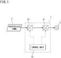
- FIG. 1 is a block diagram showing an example of a system including an inverter device according to an embodiment of the present invention.
- a photovoltaic panel 2 as a DC power supply is connected to an input end of an inverter device 1
- an AC commercial power system 3 (AC system) is connected to an output end of the inverter device 1.
- This system performs interconnection operation to convert DC power generated by the photovoltaic panel 2 to AC power and output the AC power to the commercial power system 3.
- the inverter device 1 includes a step-up circuit (DC/DC converter) 10 which receives DC power outputted from the photovoltaic panel 2, an inverter circuit (DC/AC inverter) 11 which converts power given from the step-up circuit 10 to AC power and outputs the AC power to the commercial power system 3, and a control unit 12 which controls operations of these circuits 10 and 11.
- DC/DC converter DC/DC converter
- DC/AC inverter DC/AC inverter
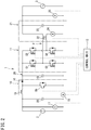
- FIG. 2 is an example of a circuit diagram of the inverter device 1.
- the step-up circuit 10 includes a DC reactor 15, a diode 16, and a switching element Qb composed of an Insulated Gate Bipolar Transistor (IGBT) or the like, to form a step-up chopper circuit.
- IGBT Insulated Gate Bipolar Transistor
- a first voltage sensor 17, a first current sensor 18, and a capacitor 26 for smoothing are provided on an input side of the step-up circuit 10.
- the first voltage sensor 17 detects a DC input voltage detection value Vg (DC input voltage value) of DC power outputted from the photovoltaic panel 2 and then inputted to the step-up circuit 10, and outputs the DC input voltage detection value Vg to the control unit 12.
- the first current sensor 18 detects a step-up circuit current detection value Iin (DC input current value) of current flowing in the DC reactor 15, and outputs the step-up circuit current detection value Iin to the control unit 12.
- a current sensor may be further provided at a stage preceding the capacitor 26.
- the control unit 12 has a function of calculating input power Pin from the DC input voltage detection value Vg and the step-up circuit current detection value Iin and performing maximum power point tracking (MPPT) control for the photovoltaic panel 2.
- MPPT maximum power point tracking
- the switching element Qb of the step-up circuit 10 is controlled so as to minimize a sum of the number of times the switching element Qb performs switching operation and the number of times the inverter circuit 11 performs switching operation, and a stop period arises. Therefore, during a period in which switching operation is performed in the step-up circuit 10, the step-up circuit 10 outputs stepped-up power to the inverter circuit 11, and during a period in which the switching operation is stopped, the step-up circuit 10 outputs, to the inverter circuit 11, DC power outputted from the photovoltaic panel 2 and then inputted to the step-up circuit 10, without stepping up the DC input voltage value thereof.
- a capacitor 19 (smoothing capacitor) for smoothing is connected to a DC bus 20 between the step-up circuit 10 and the inverter circuit 11.
- the inverter circuit 11 includes switching elements Q1 to Q4 each composed of a Field Effect Transistor (FET).
- FET Field Effect Transistor
- the switching elements Q1 to Q4 are connected to the control unit 12, and can be controlled by the control unit 12.
- the control unit 12 performs PWM control of operations of the switching elements Q1 to Q4.
- the inverter circuit 11 converts power given from the step-up circuit 10 to AC power.
- the inverter device 1 includes a filter circuit 21 between the inverter circuit 11 and the commercial power system 3.
- the filter circuit 21 is composed of two AC reactors 22 and a capacitor 23 (output smoothing capacitor) provided at a stage subsequent to the AC reactors 22.
- the filter circuit 21 has a function to remove a high-frequency component contained in AC power outputted from the inverter circuit 11.
- the AC power from which the high-frequency component has been removed by the filter circuit 21 is given to the commercial power system 3.
- the step-up circuit 10 and the inverter circuit 11 form a conversion unit which converts DC power outputted from the photovoltaic panel 2 to AC power and outputs the converted AC power to the commercial power system 3 via the filter circuit 21.
- a second current sensor 24 for detecting an inverter current detection value Iinv (current flowing in the AC reactor 22) which is a current value of output of the inverter circuit 11 is connected to the filter circuit 21.
- a second voltage sensor 25 for detecting a voltage value (system voltage detection value Va) on the commercial power system 3 side is connected between the filter circuit 21 and the commercial power system 3.
- the second current sensor 24 and the second voltage sensor 25 respectively output the detected inverter current detection value Iinv and the detected system voltage detection value Va (the voltage value of the AC system) to the control unit 12.
- the second current sensor 24 is provided at a stage preceding the capacitor 23 as shown in FIG. 2
- a third current sensor for detecting output current of the inverter device 1 may be added at a stage subsequent to the capacitor 23.
- the control unit 12 controls the step-up circuit 10 and the inverter circuit 11 based on the system voltage detection value Va, the inverter current detection value Iinv, the DC input voltage detection value Vg, and the step-up circuit current detection value Iin.
- FIG. 3 is a block diagram of the control unit 12. As shown in FIG. 3 , the control unit 12 functionally has a control processing unit 30, a step-up circuit control unit 32, an inverter circuit control unit 33, and an averaging processing unit 34.
- control unit 12 may be configured as a hardware circuit, or may be realized by software (computer program) executed by a computer.
- software for realizing a function of the control unit 12 is stored in a storage device (not shown) of the computer.
- the step-up circuit control unit 32 controls the switching element Qb of the step-up circuit 10 based on a target value and a detection value given from the control processing unit 30, thereby causing the step-up circuit 10 to output power having current corresponding to the target value.
- the inverter circuit control unit 33 controls the switching elements Q1 to Q4 of the inverter circuit 11 based on a target value and a detection value given from the control processing unit 30, thereby causing the inverter circuit 11 to output power having current corresponding to the target value.
- the control processing unit 30 receives the DC input voltage detection value Vg, the step-up circuit current detection value Iin, the system voltage detection value Va, and the inverter current detection value Iinv.
- the control processing unit 30 calculates the input power Pin and an average value ⁇ Pin> thereof from the DC input voltage detection value Vg and the step-up circuit current detection value Iin.
- the control processing unit 30 has a function to set a DC input current target value Ig* (which will be described later) based on the input power average value ⁇ Pin> and perform MPPT control for the photovoltaic panel 2, and to perform feedback control for the step-up circuit 10 and the inverter circuit 11.
- the DC input voltage detection value Vg and the step-up circuit current detection value Iin are given to the averaging processing unit 34 and the control processing unit 30.
- the averaging processing unit 34 has a function to sample, at predetermined time intervals, the DC input voltage detection value Vg and the step-up circuit current detection value Iin given from the first voltage sensor 17 and the first current sensor 18, calculate their respective average values, and give the averaged DC input voltage detection value Vg and the averaged step-up circuit current detection value Iin to the control processing unit 30.
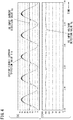
- FIG. 4 is a graph showing an example of a simulation result of temporal changes in the DC input voltage detection value Vg and the step-up circuit current detection value Iin.
- the DC input current detection value Ig is a current value detected on an input side relative to the capacitor 26.
- the DC input voltage detection value Vg, the step-up circuit current detection value Iin, and the DC input current detection value Ig vary in a half cycle of the system voltage.
- the reason why the DC input voltage detection value Vg and the DC input current detection value Ig vary periodically as shown in FIG. 4 is as follows. That is, the step-up circuit current detection value Iin greatly varies between almost 0A and a peak value in a half cycle of the AC cycle in accordance with operations of the step-up circuit 10 and the inverter circuit 11. Therefore, the variation component cannot be fully removed by the capacitor 26, and the DC input current detection value Ig is detected as pulsating current containing a component that varies in a half cycle of the AC cycle. On the other hand, output voltage of the photovoltaic panel varies depending on output current.
- the cycle of the periodic variation occurring in the DC input voltage detection value Vg is half the cycle of AC power outputted from the inverter device 1.
- the averaging processing unit 34 averages the DC input voltage detection value Vg and the step-up circuit current detection value Iin in order to suppress an influence of the above periodic variations.
- FIG. 5 is a diagram showing a manner in which the averaging processing unit 34 averages the DC input voltage detection value Vg.
- the averaging processing unit 34 samples the given DC input voltage detection value Vg a plurality of times (at timings indicated by solid dots in FIG. 5 ) at predetermined time intervals ⁇ t during a period L from a timing t1 to a timing t2, and calculates an average value of the plurality of DC input voltage detection values Vg that have been obtained.
- the averaging processing unit 34 sets the period L to half the length of the cycle of the commercial power system 3. In addition, the averaging processing unit 34 sets the time interval ⁇ t to be sufficiently shorter than half the length of the cycle of the commercial power system 3.
- the averaging processing unit 34 can accurately obtain the average value of the DC input voltage detection value Vg which periodically varies in synchronization with the cycle of the commercial power system 3, using as short a sampling period as possible.
- the time interval ⁇ t of sampling may be set at, for example, 1/100 to 1/1000 of the cycle of the commercial power system 3, or 20 microseconds to 200 microseconds.
- the averaging processing unit 34 may store the period L in advance, or may acquire the system voltage detection value Va from the second voltage sensor 25 and set the period L based on the cycle of the commercial power system 3.
- the period L is set to half the length of the cycle of the commercial power system 3.
- the average value of the DC input voltage detection value Vg can be accurately calculated at least if the period L is set to half the cycle of the commercial power system 3. This is because the DC input voltage detection value Vg periodically varies in a half cycle of the commercial power system 3 in accordance with operations of the step-up circuit 10 and the inverter circuit 11 as described above.
- the period L may be set to an integer multiple of a half cycle of the commercial power system 3, e.g., three or four times of a half cycle of the commercial power system 3.
- the voltage variation can be grasped on a cycle basis.
- the step-up circuit current detection value Iin also periodically varies in a half cycle of the commercial power system 3, as in the DC input voltage detection value Vg.
- the averaging processing unit 34 also calculates an average value of the step-up circuit current detection value Iin by the same method as in the DC input voltage detection value Vg shown in FIG. 5 .
- the control processing unit 30 sequentially calculates an average value of the DC input voltage detection value Vg and an average value of the step-up circuit current detection value Iin per the period L.
- the averaging processing unit 34 gives the calculated average value of the DC input voltage detection value Vg and the calculated average value of the step-up circuit current detection value Iin to the control processing unit 30.
- the averaging processing unit 34 calculates an average value (DC input voltage average value ⁇ Vg>) of the DC input voltage detection value Vg and an average value (step-up circuit current average value ⁇ Iin>) of the step-up circuit current detection value Iin, and using these values, the control processing unit 30 controls the step-up circuit 10 and the inverter circuit 11 while performing MPPT control for the photovoltaic panel 2. Therefore, even if DC current from the photovoltaic panel 2 varies to be unstable, the control unit 12 can accurately obtain output of the photovoltaic panel 2 as the DC input voltage average value ⁇ Vg> and the step-up circuit current average value ⁇ Iin> in which a variation component due to operation of the inverter device 1 has been removed. As a result, it becomes possible to appropriately perform MPPT control and effectively suppress reduction in power generation efficiency of the photovoltaic panel 2.
- the DC input voltage detection value Vg and the step-up circuit current detection value Iin are each sampled a plurality of times at the time intervals ⁇ t which are shorter than a half cycle of the AC system, during the period L which is set to half the length of the cycle of the commercial power system 3, and the DC input voltage average value ⁇ Vg> and the step-up circuit current average value ⁇ Iin> are calculated from a result of the sampling. Therefore, even if voltage and current of the DC current vary periodically, the DC input voltage average value ⁇ Vg> and the step-up circuit current average value ⁇ Iin> can be accurately calculated, with the sampling period shortened as much as possible.
- the control processing unit 30 sets the DC input current target value Ig* based on the above input power average value ⁇ Pin>, and calculates respective target values for the step-up circuit 10 and the inverter circuit 11 based on the set DC input current target value Ig* and the above values.
- the control processing unit 30 has a function of giving the calculated target values to the step-up circuit control unit 32 and the inverter circuit control unit 33 and performing feedback control for the step-up circuit 10 and the inverter circuit 11.
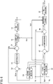
- FIG. 6 is a control block diagram for explaining the feedback control for the step-up circuit 10 and the inverter circuit 11 by the control processing unit 30.
- the control processing unit 30 includes, as function sections for controlling the inverter circuit 11, a first calculation section 41, a first adder 42, a compensator 43, and a second adder 44.
- control processing unit 30 includes, as a function section for controlling the step-up circuit 10, a second calculation section 51, a third adder 52, a compensator 53, and a fourth adder 54.
- FIG. 7 is a flowchart showing a control process for the step-up circuit 10 and the inverter circuit 11.
- the function sections shown in FIG. 6 control the step-up circuit 10 and the inverter circuit 11 by executing the process shown in the flowchart in FIG. 7 .
- control processing unit 30 calculates the present input power average value ⁇ Pin> (step S9), and compares the present input power average value ⁇ Pin> with the input power average value ⁇ Pin> that has been previously calculated, to set the DC input current target value Ig* (step S1).
- the input power average value ⁇ Pin> is calculated based on the following expression (1).
- Input power average value ⁇ Pin > ⁇ Iin ⁇ Vg >
- Iin is the step-up circuit current detection value
- Vg is the DC input voltage detection value (DC input voltage value).
- the DC input voltage average value ⁇ Vg> and the step-up circuit current average value ⁇ Iin> which are the values averaged by the averaging processing unit 34 are used.
- the control processing unit 30 gives the set DC input current target value Ig* to the first calculation section 41.
- the DC input current target value Ig* As well as the DC input current target value Ig*, the DC input voltage detection value Vg and the system voltage detection value Va are given to the first calculation section 41.
- the first calculation section 41 calculates an average value ⁇ Ia*> of an output current target value for the inverter device 1, based on the following expression (2).
- Average value ⁇ Ia * > of output current target value ⁇ Ig * ⁇ Vg / ⁇ Va > where ⁇ is a constant representing the conversion efficiency of the inverter device 1.
- the first calculation section 41 calculates an output current target value Ia* based on the following expression (3) (step S2).
- the first calculation section 41 calculates the output current target value Ia* as a sine wave having the same phase as the system voltage detection value Va.
- Output current target value Ia * ⁇ 2 ⁇ ⁇ Ia * > ⁇ sin ⁇ t
- the first calculation section 41 calculates the output current target value Ia* based on the input power average value ⁇ Pin> (an input power value of DC power) and the system voltage detection value Va.
- the first calculation section 41 calculates an inverter current target value Iinv* (a current target value for the inverter circuit) which is a current target value for controlling the inverter circuit 11, as shown by the following expression (4) (step S3).
- Inverter current target value Iinv * Ia * + s CaVa
- Ca is an electrostatic capacitance of the capacitor 23 (output smoothing capacitor), and s is the Laplace operator.
- the second term on the right-hand side is a value added in consideration of current flowing through the capacitor 23 of the filter circuit 21.
- the output current target value Ia* is calculated as a sine wave having the same phase as the system voltage detection value Va, as shown by the above expression (3). That is, the control processing unit 30 controls the inverter circuit 11 so that current Ia (output current) of AC power outputted from the inverter device 1 has the same phase as the system voltage (system voltage detection value Va).
- the first calculation section 41 After calculating the inverter current target value Iinv*, the first calculation section 41 gives the inverter current target value Iinv* to the first adder 42.
- the inverter circuit 11 is subjected to feedback control based on the inverter current target value Iinv*.
- the present inverter current detection value Iinv is given to the first adder 42.
- the first adder 42 calculates a difference between the inverter current target value Iinv* and the present inverter current detection value Iinv, and gives a result of the calculation to the compensator 43.
- the compensator 43 When the difference is given, the compensator 43 performs calculation based on based on a proportionality coefficient or the like, and further adds the system voltage Va by the second adder 44, thereby calculating an inverter voltage reference value Vinv# that allows the difference to converge so that the inverter current detection value Iinv becomes the inverter current target value Iinv*.
- a control signal obtained by comparing the inverter voltage reference value Vinv# with an output voltage target value Vo* for the DC/DC converter given from the first calculation section 41 is given to the inverter circuit control unit 33, thereby causing the inverter circuit 11 to output voltage according to the inverter voltage reference value Vinv#.
- the voltage outputted from the inverter circuit 11 is given to the AC reactor 22, and then fed back as a new inverter current detection value Iinv. Then, a difference between the inverter current target value Iinv* and the inverter current detection value Iinv is calculated again by the first adder 42, and the inverter circuit 11 is controlled based on the difference as described above.
- the inverter circuit 11 is subjected to feedback control based on the inverter current target value Iinv* and the inverter current detection value Iinv (step S4).
- the second calculation section 51 calculates an inverter output voltage target value Vinv* (a voltage target value for the inverter circuit) based on the following expression (5) (step S5).
- Inverter output voltage target value Vinv * Va * + ZaIinv *
- Za is an impedance of the AC reactor.
- the second term on the right-hand side in expression (5) and the second term and the third term on the right-hand side in expression (5a) are values added in consideration of voltage generated between both ends of the AC reactor 22.
- the inverter output voltage target value Vinv* is set based on the inverter current target value Iinv* which is the current target value for controlling the inverter circuit 11 so that current of AC power outputted from the inverter device 1 has the same phase as the system voltage detection value Va.
- the output target values (Iinv*, Vinv*) for the inverter circuit 11 which are target values on the AC side are set at a bridge output end of the inverter circuit 11, i.e., a circuit connection point P between the inverter circuit 11 and the filter circuit 21.
- the system interconnection is performed such that a point where the target values are set is moved to a stage preceding the original system interconnection point (a circuit connection point between the commercial power system 3 and the filter circuit 21), whereby appropriate system interconnection is finally reached.
- the second calculation section 51 compares the voltage Vg or preferably the following DC voltage Vgf, as voltage V DC on the DC power supply side, with an absolute value of the inverter output voltage target value Vinv*, and determines the greater one to be the step-up circuit voltage target value Vo* as shown by the following expression (6) (step S6).
- the second calculation section 51 calculates a step-up circuit current target value Iin* based on the following expression (7) (step S7).
- Step ⁇ up circuit current target value Iin * Iinv * ⁇ Vinv * + s C Vo * ⁇ Vo * / Vg ⁇ ZIin
- C is an electrostatic capacitance of the capacitor 19 (smoothing capacitor), and s is the Laplace operator.
- Iin * Iinv * ⁇ Vinv * + C ⁇ d Vo * / dt ⁇ Vo * / Vg ⁇ R + sL Iin
- Iin * Iinv * ⁇ Vinv * + Ic ⁇ Vo * / Vg ⁇ ZIin
- a term added to a product of the inverter current target value Iinv* and the inverter output voltage target value Vinv* is a value added in consideration of reactive power passing through the capacitor 19. That is, consideration of the reactive power in addition to the power target value for the inverter circuit 11 allows for more accurate calculation of the value of Iin*.
- the second calculation section 51 After calculating the step-up circuit current target value Iin*, the second calculation section 51 gives the step-up circuit current target value Iin* to the third adder 52.
- the step-up circuit 10 is subjected to feedback control based on the step-up circuit current target value Iin*.
- the present step-up circuit current detection value Iin is given to the third adder 52.
- the third adder 52 calculates a difference between the step-up circuit current target value Iin* and the present step-up circuit current detection value Iin, and gives a result of the calculation to the compensator 53.
- the compensator 53 performs calculation based on a proportionality coefficient or the like, and further subtracts the resultant value from the DC input voltage detection value Vg by the fourth adder 54, thereby calculating a step-up circuit voltage reference value Vbc# that allows the difference to converge so that the step-up circuit current detection value Iin becomes the step-up circuit current target value Iin*.
- a control signal obtained by comparing the step-up circuit voltage reference value Vbc# with the output voltage target value Vo* for the DC/DC converter given from the first calculation section 41 is given to the step-up circuit control unit 32, thereby causing the step-up circuit 10 to output voltage according to the step-up circuit voltage reference value Vbc#.
- the power outputted from the step-up circuit 10 is given to the DC reactor 15, and then fed back as a new step-up circuit current detection value Iin. Then, a difference between the step-up circuit current target value Iin* and the step-up circuit current detection value Iin is calculated again by the third adder 52, and the step-up circuit 10 is controlled based on the difference as described above.
- step-up circuit 10 is subjected to feedback control based on the step-up circuit current target value Iin* and the step-up circuit current detection value Iin (step S8).
- control processing unit 30 calculates the present input power average value ⁇ Pin> based on the above expression (1) (step S9).
- the control processing unit 30 Based on comparison with the input power average value ⁇ Pin> that has been previously calculated, the control processing unit 30 sets the DC input current target value Ig* so that the input power average value ⁇ Pin> becomes a maximum value (follows the maximum power point).
- control processing unit 30 controls the step-up circuit 10 and the inverter circuit 11 while performing MPPT control for the photovoltaic panel 2.
- control processing unit 30 performs feedback control for the inverter circuit 11 and the step-up circuit 10 by the current target values.
- FIG. 8 is graphs in which (a) shows an example of a simulation result of the step-up circuit current target value Iin* calculated in the above feedback control by the control processing unit 30, and the step-up circuit current detection value Iin obtained when control is performed in accordance with the step-up circuit current target value Iin*, and (b) shows an example of a simulation result of the step-up circuit voltage target value Vo* calculated in the above feedback control by the control processing unit 30, and a step-up circuit voltage detection value Vo obtained when control is performed in accordance with the step-up circuit voltage target value Vo*.
- step-up circuit current detection value Iin is controlled along the step-up circuit current target value Iin* by the control processing unit 30.
- the step-up circuit voltage target value Vo* varies so as to follow an absolute value of the inverter output voltage target value Vinv* during a period in which the absolute value of the inverter output voltage target value Vinv* is generally equal to or greater than the DC input voltage detection value Vg, and follow the DC input voltage detection value Vg during the other period.
- step-up circuit voltage detection value Vo is controlled along the step-up circuit voltage target value Vo* by the control processing unit 30.
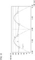
- FIG. 9 is a diagram showing an example of the inverter output voltage target value Vinv*.
- the vertical axis indicates voltage and the horizontal axis indicates time.
- a broken line indicates a voltage waveform of the commercial power system 3
- a solid line indicates a waveform of the inverter output voltage target value Vinv*.
- the inverter circuit 11 outputs power, using the inverter output voltage target value Vinv* shown in FIG. 9 as a voltage target value, through the control according to the flowchart in FIG. 7 .
- the inverter circuit 11 outputs power having voltage according to the waveform of the inverter output voltage target value Vinv* shown in FIG. 9 .
- the two waveforms have almost the same voltage value and the same frequency, but the phase of the inverter output voltage target value Vinv* leads the phase of voltage of the commercial power system 3 by several degrees.
- the control processing unit 30 of the present embodiment causes the phase of the inverter output voltage target value Vinv* to lead the phase of voltage of the commercial power system 3 by about three degrees while executing the feedback control for the step-up circuit 10 and the inverter circuit 11, as described above.
- the degree of angle by which the phase of the inverter output voltage target value Vinv* is caused to lead the phase of voltage of the commercial power system 3 may be several degrees, and as described later, the degree of angle is set within such a range that the phase of a voltage waveform of a difference from a voltage waveform of the commercial power system 3 leads the phase of the voltage waveform of the commercial power system 3 by 90 degrees.
- the degree of the phase leading angle is set to be greater than 0 degrees and smaller than 10 degrees.
- the degree of the phase leading angle is determined by the system voltage detection value Va, the inductance La of the AC reactor 22, and the inverter current target value Iinv* as shown by the above expression (5).
- the system voltage detection value Va and the inductance La of the AC reactor 22 are fixed values that are not control targets. Therefore, the degree of the phase leading angle is determined by the inverter current target value Iinv*.
- the inverter current target value Iinv* is determined by the output current target value Ia* as shown by the above expression (4). As the output current target value Ia* increases, a phase leading component of the inverter current target value Iinv* increases, and a leading angle (phase leading angle) of the inverter output voltage target value Vinv* increases.
- the step-up circuit control unit 32 controls the switching element Qb of the step-up circuit 10.
- the inverter circuit control unit 33 controls the switching elements Q1 to Q4 of the inverter circuit 11.
- the step-up circuit control unit 32 and the inverter circuit control unit 33 respectively generate a step-up circuit carrier wave and an inverter circuit carrier wave, and respectively modulate these carrier waves with the step-up circuit voltage reference value Vbc# and the inverter voltage reference value Vinv# which are target values given from the control processing unit 30, to generate drive waveforms for driving each switching element.
- the step-up circuit control unit 32 and the inverter circuit control unit 33 control each switching element based on the drive waveforms, thereby causing the step-up circuit 10 and the inverter circuit 11 to output AC powers having current waveforms approximate to the step-up circuit current target value Iin* and the inverter current target value Iinv*, respectively.
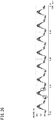
- FIG. 10 (a) is a graph showing comparison between the step-up circuit carrier wave and a waveform of the step-up circuit voltage reference value Vbc#.
- the vertical axis indicates voltage and the horizontal axis indicates time.
- the wavelength of the step-up circuit carrier wave is elongated as compared to the actual wavelength.
- the step-up circuit carrier wave generated by the step-up circuit control unit 32 is a triangle wave having a minimum value of "0", and has an amplitude A1 set at the step-up circuit voltage target value Vo* given from the control processing unit 30.
- the frequency of the step-up circuit carrier wave is set by the step-up circuit control unit 32 in accordance with a control command from the control processing unit 30, so as to realize a predetermined duty ratio.
- the step-up circuit voltage target value Vo* varies so as to follow an absolute value of the inverter output voltage target value Vinv* during a period W1 in which the absolute value of the inverter output voltage target value Vinv* is generally equal to or greater than the DC input voltage detection value Vg, and follow the DC input voltage detection value Vg during the other period. Therefore, the amplitude A1 of the step-up circuit carrier wave also varies in accordance with the step-up circuit voltage target value Vo*.
- the DC input voltage detection value Vg is 250 volts
- the amplitude of voltage of the commercial power system 3 is 288 volts.
- a waveform (hereinafter, may be referred to as a step-up circuit reference wave Vbc#) of the step-up circuit voltage reference value Vbc# corresponds to a value calculated based on the step-up circuit current target value Iin* by the control processing unit 30, and has a positive value during the period W1 in which the absolute value of the inverter output voltage target value Vinv* is greater than the DC input voltage detection value Vg.
- the step-up circuit reference wave Vbc# has a waveform approximate to the shape of a waveform created by the step-up circuit voltage target value Vo*, and crosses the step-up circuit carrier wave.
- the step-up circuit control unit 32 compares the step-up circuit carrier wave with the step-up circuit reference wave Vbc#, and generates a drive waveform for driving the switching element Qb so as to be turned on during a period in which the step-up circuit reference wave Vbc# which is a target value for voltage between both ends of the DC reactor 15 is equal to or greater than the step-up circuit carrier wave, and to be turned off during a period in which the step-up circuit reference wave Vbc# is equal to or smaller than the carrier wave.
- FIG. 10 shows the drive waveform for driving the switching element Qb, generated by the step-up circuit control unit 32.
- the vertical axis indicates voltage and the horizontal axis indicates time.
- the horizontal axis in (b) of FIG. 10 coincides with that in (a) of FIG. 10 .
- the drive waveform indicates switching operation of the switching element Qb.
- the switching element Qb is caused to perform switching operation in accordance with the drive waveform.
- the drive waveform forms a control command to turn off the switching element when the voltage is 0 volts and turn on the switching element when the voltage is a plus voltage.
- the step-up circuit control unit 32 generates the drive waveform so that the switching operation is performed during the period W1 in which the absolute value of the inverter output voltage target value Vinv* is equal to or greater than the DC input voltage detection value Vg. Therefore, in a range in which the absolute value is equal to or smaller than the DC input voltage detection value Vg, the switching element Qb is controlled to stop the switching operation.
- Each pulse width is determined by an intercept of the step-up circuit carrier wave which is a triangle wave. Therefore, the pulse width is greater at a part where voltage is higher.
- the step-up circuit control unit 32 modulates the step-up circuit carrier wave with the step-up circuit reference wave Vbc#, to generate the drive waveform representing pulse widths for switching.
- the step-up circuit control unit 32 performs PWM control for the switching element Qb of the step-up circuit 10, based on the generated drive waveform.
- a drive waveform inverted from the drive waveform for the switching element Qb is used for the switching element Qbu.
- a dead time of about 1 microsecond is provided at a part where a drive pulse for the switching element Qbu shifts from OFF to ON.
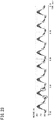
- FIG. 11 (a) is a graph showing comparison between the inverter circuit carrier wave and a waveform of the inverter voltage reference value Vinv#.
- the vertical axis indicates voltage and the horizontal axis indicates time.
- the wavelength of the inverter circuit carrier wave is elongated as compared to the actual wavelength.
- the inverter circuit carrier wave generated by the inverter circuit control unit 33 is a triangle wave having an amplitude center at 0 volts, and a one-side amplitude thereof is set at the step-up circuit voltage target value Vo* (a voltage target value for the capacitor 23). Therefore, the inverter circuit carrier wave has a period in which an amplitude A2 thereof is twice (500 volts) as great as the DC input voltage detection value Vg and a period in which the amplitude A2 is twice (576 volts at maximum) as great as voltage of the commercial power system 3.
- the frequency thereof is set by the inverter circuit control unit 33 in accordance with a control command from the control processing unit 30, or the like, so as to realize a predetermined duty ratio.
- the step-up circuit voltage target value Vo* varies to follow an absolute value of the inverter output voltage target value Vinv* during the period W1 in which the absolute value of the inverter output voltage target value Vinv* is generally equal to or greater than the DC input voltage detection value Vg, and follow the DC input voltage detection value Vg during the other period, i.e., a period W2. Therefore, the amplitude A2 of the inverter circuit carrier wave also varies in accordance with the step-up circuit voltage target value Vo*.
- a waveform (hereinafter, may be referred to as an inverter circuit reference wave Vinv#) of the inverter voltage reference value Vinv# corresponds to a value calculated based on the inverter current target value Iinv* by the control processing unit 30, and is set to have generally the same amplitude as the voltage amplitude (288 volts) of the commercial power system 3. Therefore, the inverter circuit reference wave Vinv# crosses the inverter circuit carrier wave in a range where the voltage value is between -Vg and +Vg.
- the inverter circuit control unit 33 compares the inverter circuit carrier wave with the inverter circuit reference wave Vinv#, and generates drive waveforms for driving the switching elements Q1 to Q4 so as to be turned on during a period in which the inverter circuit reference wave Vinv# which is a voltage target value is equal to or greater than the inverter circuit carrier wave, and to be turned off during a period in which the inverter circuit reference wave Vinv# is equal to or smaller than the carrier wave.
- FIG. 11 shows the drive waveform for driving the switching element Q1, generated by the inverter circuit control unit 33.
- the vertical axis indicates voltage and the horizontal axis indicates time.
- the horizontal axis in (b) of FIG. 11 coincides with that in (a) of FIG. 11 .
- the inverter circuit control unit 33 generates the drive waveform so that the switching operation is performed in the range W2 in which voltage of the inverter circuit reference wave Vinv# is between -Vg and +Vg. Therefore, in the other range, the switching element Q1 is controlled to stop the switching operation.
- FIG. 11 shows the drive waveform for driving the switching element Q3, generated by the inverter circuit control unit 33.
- the vertical axis indicates voltage and the horizontal axis indicates time.
- the inverter circuit control unit 33 compares the carrier wave with a waveform indicated by a broken line in (a) of FIG. 11 , which is inverted from the inverter circuit reference wave Vinv#, to generate the drive waveform for the switching element Q3.
- the inverter circuit control unit 33 generates the drive waveform so that the switching operation is performed in the range W2 in which voltage of (a waveform inverted from) the inverter circuit reference wave Vinv# is between -Vg and +Vg. Therefore, in the other range, the switching element Q3 is controlled to stop the switching operation.
- the inverter circuit control unit 33 generates, as the drive waveform for the switching element Q2, a waveform inverted from the drive waveform for the switching element Q1, and generates, as the drive waveform for the switching element Q4, a waveform inverted from the drive waveform for the switching element Q3.
- the inverter circuit control unit 33 modulates the inverter circuit carrier wave with the inverter circuit reference wave Vinv#, to generate the drive waveforms representing pulse widths for switching.
- the inverter circuit control unit 33 performs PWM control for the switching elements Q1 to Q4 of the inverter circuit 11, based on the generated drive waveforms.
- the step-up circuit control unit 32 of the present embodiment causes the step-up circuit 10 to output power so that current flowing in the DC reactor 15 coincides with the step-up circuit current target value Iin*.
- the step-up circuit 10 is caused to perform switching operation during the period W1 ( FIG. 10 ) in which an absolute value of the inverter output voltage target value Vinv* is generally equal to or greater than the DC input voltage detection value Vg.
- the step-up circuit 10 outputs power having voltage equal to or greater than the DC input voltage detection value Vg and approximate to the absolute value of the inverter output voltage target value Vinv*, during the period W1.
- the step-up circuit control unit 32 stops the switching operation of the step-up circuit 10. Therefore, during the period in which the absolute value is equal to or smaller than the DC input voltage detection value Vg, the step-up circuit 10 outputs, to the inverter circuit 11, DC power outputted from the photovoltaic panel 2 without stepping up the DC input voltage value thereof.
- the inverter circuit control unit 33 of the present embodiment causes the inverter circuit 11 to output power so that current flowing in the AC reactor 22 coincides with the inverter current target value Iinv*.
- the inverter circuit 11 is caused to perform switching operation during the period W2 ( FIG. 11 ) in which the inverter output voltage target value Vinv* is generally between -Vg and +Vg. That is, the inverter circuit 11 is caused to perform switching operation during a period in which an absolute value of the inverter output voltage target value Vinv* is equal to or smaller than the DC input voltage detection value Vg.
- the inverter circuit 11 performs switching operation to output AC power approximate to the inverter output voltage target value Vinv*.
- the inverter circuit control unit 33 stops the switching operation of the inverter circuit 11. During this period, power stepped up by the step-up circuit 10 is given to the inverter circuit 11. Therefore, the inverter circuit 11 whose switching operation is stopped outputs the power given from the step-up circuit 10, without stepping down the voltage thereof.
- the inverter device 1 of the present embodiment causes the step-up circuit 10 and the inverter circuit 11 to perform switching operations so as to be alternately switched therebetween, and superimposes their respective output powers on each other, thereby outputting AC power having a voltage waveform approximate to the inverter output voltage target value Vinv*.
- control is performed so that the step-up circuit 10 is operated in the case of outputting voltage corresponding to the part where the absolute value of the inverter output voltage target value Vinv* is higher than the DC input voltage detection value Vg, and the inverter circuit 11 is operated in the case of outputting voltage corresponding to the part where the absolute value of the inverter output voltage target value Vinv* is lower than the DC input voltage detection value Vg. Therefore, since the inverter circuit 11 does not step down the power that has been stepped up by the step-up circuit 10, a potential difference in stepping down of the voltage can be reduced, whereby loss due to switching of the step-up circuit is reduced and AC power can be outputted with increased efficiency.
- both the step-up circuit 10 and the inverter circuit 11 operate based on the inverter output voltage target value Vinv* set by the control unit 12, occurrence of deviation or distortion between power of the step-up circuit and power of the inverter circuit which are outputted so as to be alternately switched can be suppressed.
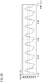
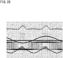
- FIG. 12 is a diagram showing examples of the reference waves and the drive waveforms for the switching elements, and an example of a current waveform of AC power outputted from the inverter device 1.
- FIG. 12 shows graphs of, from the uppermost side, the reference wave Vinv# and the carrier wave for the inverter circuit, the drive waveform for the switching element Q1, the reference wave Vbc# and the carrier wave for the step-up circuit, the drive waveform for the switching element Qb, and the target value and an actual measured value of a current waveform of AC power outputted from the inverter device 1.
- the horizontal axes of these graphs indicate time, and coincide with each other.
- output current is controlled so that an actual measured value Ia thereof coincides with a target value Ia*.
- the step-up circuit is controlled so that current flowing in the DC reactor 15 coincides with the current target value Iin* calculated based on the above expression (7).
- voltages of the step-up circuit and the inverter circuit have waveforms as shown in (b) of FIG. 8 , and it becomes possible to perform such an operation that high-frequency switching operations of the step-up circuit 10 and the inverter circuit 11 have respective stop periods and the switching operations are performed generally alternately.
- the step-up circuit 10 and the inverter circuit 11 "alternately" perform high-frequency switching so that their respective periods of high-frequency switching do not overlap each other.
- the loss can be reduced, leading to enhancement in the efficiency.
- the step-up circuit 10 and the inverter circuit 11 of the present embodiment output AC power having a voltage waveform approximate to the inverter output voltage target value Vinv*, to the filter circuit 21 connected at the subsequent stage, through the control by the control unit 12.
- the inverter device 1 outputs AC power to the commercial power system 3 via the filter circuit 21.
- the inverter output voltage target value Vinv* is generated by the control processing unit 30 so as to have a voltage phase leading the voltage phase of the commercial power system 3 by several degrees as described above.
- AC voltage outputted by the step-up circuit 10 and the inverter circuit 11 also has a voltage phase leading the voltage phase of the commercial power system 3 by several degrees.
- the AC voltage from the step-up circuit 10 and the inverter circuit 11 is applied to one end of the AC reactor 22 ( FIG. 2 ) of the filter circuit 21, and voltage of the commercial power system 3 is applied to the other end.
- voltages having phases shifted from each other by several degrees are applied to the respective ends of the AC reactor 22.
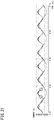
- FIG. 13 (a) is a graph showing voltage waveforms of AC voltage outputted from the inverter circuit 11, the commercial power system 3, and voltage between both ends of the AC reactor 22.
- the vertical axis indicates voltage and the horizontal axis indicates time.
- (b) is a graph showing a waveform of current flowing in the AC reactor 22.
- the vertical axis indicates current and the horizontal axis indicates time.
- the horizontal axis in (b) of FIG. 13 coincides with that in (a) of FIG. 13 .
- the current phase of the AC reactor 22 lags the voltage phase thereof by 90 degrees. Therefore, as shown in (b) of FIG. 13 , the current phase of AC power outputted through the AC reactor 22 is synchronized with the current phase of the commercial power system 3.
- phase of voltage outputted from the inverter circuit 11 leads the phase of the commercial power system 3 by several degrees, the phase of current outputted from the inverter circuit 11 coincides with the phase of current of the commercial power system 3.
- the phase of a current waveform outputted from the inverter device 1 coincides with the voltage phase of the commercial power system 3.
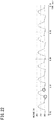
- (a) is an example of the AC output waveform of the inverter device 1 according to the above embodiment.
- the step-up circuit current target value Iin* in this case is given by expression (7), for example.
- AC output current having a sine waveform synchronized with the system voltage is obtained.
- the power factor is 0.997 and an overall current distortion rate is 4.6%, and thus they are adequate for respective criterion values in system interconnection which are generally set at 0.95 or higher and at 5% or lower, respectively.
- a second-order distortion rate is 2.6% (adequate for 3% or lower)
- a third-order distortion rate is 2.9% (adequate for 3% or lower)
- a fifth-order distortion rate is 0.3% (adequate for 3% or lower).
- (b) of FIG. 14 is an example of an AC output waveform obtained when the inverter device 1 is controlled in accordance with a step-up circuit current target value prescribed by the following expression (9).
- Iin * Ia * ⁇ Va / Vg
- the AC output current has a waveform the peak of which is clearly distorted.
- the power factor is 0.947 (inadequate for 0.95 or higher) and the overall current distortion rate is 8.3% (inadequate for 5% or lower), and thus both of them are not adequate for the above criterion values in system interconnection.
- a second-order distortion rate is 3.5% (inadequate for 3% or lower)
- a third-order distortion rate is 4.3% (inadequate for 3% or lower)
- a fifth-order distortion rate is 4.6% (inadequate for 3% or lower).
- FIG. 15 is a block diagram showing an example of a power storage system including the conversion device 1R.
- a storage battery 2 is connected to an output end of the conversion device 1R, and the commercial power system 3 (AC system) is connected to an input end of the conversion device 1R.
- the power storage system is capable of converting power provided from the commercial power system 3, from AC to DC, and storing the converted power in the storage battery 2.
- the conversion device 1R includes: an AC/DC converter 11u which converts AC power received from the commercial power system 3 to DC power; a step-down circuit (DC/DC converter) 10d which steps down output voltage of the AC/DC converter 11u; and the control unit 12 which controls operations of these circuits 10d and 11u. As is obvious from comparison with FIG. 1 , the direction of energy flow is reversed.
- FIG. 16 is an example of a circuit diagram of the conversion device 1R.
- the photovoltaic panel 2 in FIG. 2 is replaced with a storage battery 2B.
- the step-up circuit 10 in FIG. 2 is replaced with the step-down circuit 10d
- the inverter circuit 11 in FIG. 2 is replaced with the AC/DC converter 11u which is capable of also step-up operation in cooperation with the AC reactor 22 though the components thereof are the same.
- the step-down circuit 10d is provided with a switching element Qb2 in parallel with the same diode 16 as in FIG. 2 .
- the switching element Qb2 the shown IGBT or FET can be used, for example.
- the other configuration of the conversion device 1R is basically the same as that of the inverter device 1 in FIG. 2 . Therefore, the conversion device 1R has a bidirectional property, and is capable of performing the same operation as in the inverter device 1 in FIG. 2 when a photovoltaic panel is connected. In addition, the conversion device 1R is also capable of performing autonomous operation by converting DC power of the storage battery 2B to AC power.
- the switching element Qb2 is controlled by the control unit 12 so as to be OFF constantly (in the case of IGBT) or so as to be turned on alternately with the switching element Qb (in the case of FET).
- the step-down circuit 10d serves as a step-up circuit
- the AC/DC converter 11u serves as an inverter circuit.
- the control unit 12 can perform synchronous rectification by controlling operations of the switching elements Q1 to Q4. In addition, by performing PWM control under the presence of the AC reactor 22, the control unit 12 can perform rectification while performing step-up operation.
- the AC/DC converter 11u converts AC power given from the commercial AC system 3 to DC power.
- the step-down circuit 10d forms a step-down chopper circuit.
- the switching elements Qb and Qb2 are controlled by the control unit 12.
- the switching operation of the step-down circuit 10d is controlled so that a period in which the step-down circuit 10d performs switching operation and a period in which the AC/DC converter 11u performs switching operation are alternately switched. Therefore, during a period in which the step-down circuit 10d performs switching operation, the step-down circuit 10d outputs stepped-down voltage to the storage battery 2B, and during a period in which the step-down circuit 10d stops the switching operation (the switching element Qb is OFF and the switching element Qb2 is ON), the step-down circuit 10d gives DC voltage outputted from the AC/DC converter 11u and inputted to the step-down circuit 10d, to the storage battery 2 via the DC reactor 15.
- FIG. 17 is a voltage waveform diagram conceptually showing operation of the conversion device 1R.
- FIG. 17 shows an example of an absolute value of an AC input voltage target value Vinv* for the AC/DC converter 11u. This generally corresponds to a full-wave-rectified waveform based on the commercial AC.
- a two-dot dashed line indicates DC voltage Vg for charging.
- the AC/DC converter 11u performs switching operation and performs step-up operation in cooperation with the AC reactor 22.
- step-down circuit 10d the switching element Qb is OFF and the switching element Qb2 is ON, and the step-down circuit 10d stops step-down operation.
- thin stripes shown in (b) of FIG. 17 are actually a PWM pulse train, and the duty thereof varies in accordance with the absolute value of the AC input voltage target value Vinv*. Therefore, if the voltage in this state is applied to the DC/DC converter, input voltage of the DC/DC converter, i.e., voltage of the DC bus 20 and voltage of the capacitor 19 have waveforms as shown in (c) of FIG. 17 .
- the AC/DC converter 11u stops switching, and instead, the step-down circuit 10d operates.
- the switching mentioned here means high-frequency switching at about 20kHz, for example, and does not mean switching at such a low frequency (twice as high as the commercial frequency) that is used for performing synchronous rectification.
- the switching elements Q1 and Q4 are ON and the switching elements Q2 and Q3 are OFF, and during a period in which the sign of current in the AC/DC converter 11u is negative, ON and OFF of these switching elements are inverted.
- the frequency of the inversion is twice as high as the commercial frequency, and thus is very low as compared to the high-frequency switching frequency. Therefore, loss due to the ON/OFF inversion is extremely small.
- the step-down circuit 10d performs step-down operation.
- Thin stripes shown in (d) of FIG. 17 are actually a PWM pulse train, and the duty thereof varies in accordance with the absolute value of the AC input voltage target value Vinv*.
- desired DC voltage Vg shown in (e) of FIG. 17 is obtained.
- the step-down circuit 10d operates, and during the other period, switching in the step-down circuit 10d is stopped, whereby switching loss in the step-down circuit 10d can be reduced.
- the AC/DC converter 11u and the step-down circuit 10d alternately perform switching operations, and when one of them operates, the other one stops switching. That is, for each of the AC/DC converter 11u and the step-down circuit 10d, a period in which switching is stopped arises.
- the AC/DC converter 11u operates in a region other than the peak of the absolute value of the AC input voltage target value Vinv* and the vicinity thereof, voltage at which the AC/DC converter 11u performs switching is relatively low. This also contributes to reduction in switching loss. Thus, switching loss in the conversion device 1R as a whole can be greatly reduced.
- Control of the conversion device 1R can be considered to be similar control obtained by reversing the direction of the control in system interconnection by the inverter device 1 in FIG. 2 .
- This control is suitable for, with use of the conversion device 1R which can perform the same system interconnection as in the inverter device 1, enhancing the efficiency of the conversion device 1R also in the reversed operation.
- Iinv * Ia * ⁇ Ica
- the AC input voltage target value Vinv* corresponding to expression (5) is represented as follows.
- Vinv * Va ⁇ Za Iinv *
- the input target values (Iinv*, Vinv*) for the AC/DC converter 11u which are AC-side target values are set at a circuit connection point P between the AC/DC converter 11u and the filter circuit 21. Therefore, as in the case of performing system interconnection, a point where the target values are set is moved to a stage (AC/DC converter 11u side) preceding to a circuit connection point between the commercial power system 3 and the conversion device 1R. By such, as it were, "reverse" system interconnection, appropriate interconnection between AC and DC is performed.
- Vgf i.e., (Vg - Z Iin) in expression (6)
- Vgr i.e., (Vg + Z Iin)
- Iin * Iinv * ⁇ Vinv * ⁇ Ic ⁇ Vo * / Vg + ZIin
- a term added to a product of the AC input current target value Iinv* and the AC input voltage target value Vinv* is a value added in consideration of reactive power passing through the capacitor 19. That is, consideration of the reactive power in addition to the power target value for the AC/DC converter 11u allows for more accurate calculation of the value of Iin*.
- control unit 12 performs control so that the step-down circuit 10d is operated in the case of outputting voltage corresponding to the part where the absolute value of the AC input voltage target value Vinv* for the AC/DC converter 11u is higher than the DC voltage (Vg + Z Iin), and the AC/DC converter 11u is operated in the case of outputting voltage corresponding to the part where the absolute value of the AC input voltage target value Vinv* for the AC/DC converter 11u is lower than the DC voltage (Vg + Z Iin). Therefore, a potential difference in power stepped up by the AC/DC converter 11u can be reduced, and loss due to switching of the AC/DC converter 11u and the step-down circuit 10d is reduced, whereby DC power can be outputted with increased efficiency.
- both the step-down circuit 10d and the AC/DC converter 11u operate based on the target values set by the control unit 12, occurrence of phase-deviation or distortion in AC current inputted to the AC/DC converter 11u can be suppressed even if operation is performed so as to alternately switch the high-frequency switching period between the two circuits.
- the conversion device 1R can perform the same system interconnection operation as in the inverter device 1 in FIG. 2 . Therefore, it is possible to realize an efficient conversion device that can be used in both directions of DC/AC conversion to perform system interconnection, and AC/DC conversion.
- FIG. 16 an example in which FETs are used as the switching elements composing the AC/DC converter 11u has been shown.
- IGBTs instead of FETs, IGBTs may be used as shown in FIG. 14 .
- IGBTs synchronous rectification cannot be performed. Therefore, when high-frequency switching of the AC/DC converter 11u is stopped, the AC/DC converter 11u operates as a full-bridge rectification circuit by means of the diodes included in the elements.
- FIG. 18 is a diagram showing the voltage target value Vo* as an example of the DC bus voltage (voltage of the DC bus 20 in FIG. 2 and FIG. 16 ).
- the horizontal axis indicates time and the vertical axis indicates voltage.
- Vo* is represented as follows.
- Vo * Max Vg ⁇ ZIin , absolute value of Vinv *
- Vo* has a waveform obtained by combining: a part (absolute value of Vinv*), of an AC waveform, at the peak value thereof and in the vicinity of the peak value; and a DC waveform (Vg - ZIin).
- a point (indicated by a dot-line circle in FIG. 18 ) where the AC waveform and the DC waveform are connected to each other is a discontinuity point with no smoothness. If slight oscillation of current and voltage occurs from such a discontinuity point as a start point, the slight oscillation interferes with a feedback system in the control unit 12, to cause a little greater oscillation, and this may lead to slight distortion of output current.
- Vo* Vox * + Vcp
- Vcp can be given by the following function, for example.
- Vcp a ⁇ exp ⁇ Vgf ⁇ Vinv * / b
- a is a value proportional to Vox*
- b is a constant.
- FIG. 19 An upper graph in FIG. 19 is an example of a waveform of the DC bus voltage before continuity compensation. In this graph, change in voltage is shown in an enlarged manner as compared to FIG. 18 .
- a lower graph in FIG. 19 is an example of a waveform based on the compensation term.
- FIG. 20 is a waveform of the DC bus voltage after continuity compensation, obtained by adding the compensation term (lower graph) to the DC bus voltage (upper graph) in FIG. 19 .
- the compensation term acts to add a compensation value in a positive direction, at a timing at which the AC waveform and the DC waveform should have been connected to each other to form a discontinuity point.
- the control unit 12 adds the compensation value in a positive direction at the timing that should have corresponded to the discontinuity point, and outputs the resultant value, whereby the discontinuity point can be changed to a continuity point as shown in FIG. 20 .
- a discontinuity point of voltage of the DC bus can be corrected and continuity can be achieved.
- the compensation value is represented by, for example, a spire waveform signal as shown in FIG. 19 .
- the spire waveform signal is represented by a function of expression (11) which has a peak at the discontinuity point and becomes close to zero as a distance from the discontinuity point increases.
- the compensation value in the control unit 12 is incorporated into in the voltage target value of the DC bus for the step-up circuit 10 (first converter).
- the compensation value is incorporated into the voltage target value of the DC bus for the AC/DC converter 11u from the control unit 12. In this way, since the compensation value is incorporated into the voltage target value, it is possible to change the discontinuity point to a continuity point by changing the voltage target value without adding hardware, in either the case of DC to AC or the opposite case.
- FIG. 21 , FIG. 22 , and FIG. 23 are waveform diagrams showing examples of the detection values in the DC-to-AC conversion device in the case where continuity compensation is not performed, as a reference.
- a waveform with a shorter wavelength is a waveform of current flowing through the DC reactor 15, i.e., the step-up circuit current detection value Iin, and a waveform with a longer wavelength is a waveform of the output current Ia.
- FIG. 22 is a waveform diagram of the voltage target value Vo* for the step-up circuit 10.
- FIG. 23 is a waveform diagram of the step-up circuit voltage detection value Vo. As shown at a circle mark in each diagram, it is found that oscillation starting from the discontinuity point in FIG. 22 occurs in Iin ( FIG. 21 ) and Vo ( FIG. 23 ).
- FIG. 24 , FIG. 25 , and FIG. 26 are waveforms showing examples of the detection values in the DC-to-AC conversion device in the case where continuity compensation is performed.
- a waveform with a shorter wavelength is a waveform of current flowing through the DC reactor 15, i.e., the step-up circuit current detection value Iin, and a waveform with a longer wavelength is a waveform of the output current Ia.
- FIG. 25 is a waveform diagram of the voltage target value Vo* for the step-up circuit 10.
- FIG. 26 is a waveform diagram of the step-up circuit voltage detection value Vo. As shown at a circle mark in each diagram, it is found that, although extremely small oscillation starting from the discontinuity point in FIG. 23 occurs in Iin ( FIG. 24 ) and Vo ( FIG. 26 ), the oscillation is obviously reduced as compared to FIG. 21 and FIG. 23 .
- FIG. 27 and FIG. 28 are experimental examples of waveforms with no compensation term and waveforms with the compensation term.
- the uppermost waveform is a waveform of the DC bus. Comparing the waveforms of the DC bus in FIG. 27 and FIG. 28 , oscillation starting from the discontinuity point occurs in FIG. 27 , but the oscillation is obviously reduced in FIG. 28 .
Description
- The present invention relates to a conversion device that performs conversion from DC to AC or conversion from AC to DC.
- Generally, a conversion device that outputs AC power based on a DC power supply includes: a step-up circuit which steps up voltage of the DC power supply to a constant level equal to or higher than a required AC peak value and outputs the stepped-up voltage to a DC bus; and an inverter which modulates the constant voltage of the DC bus so as to have an AC waveform through switching, and outputs the modulated voltage. The step-up circuit and the inverter each perform high-frequency switching constantly. Due to the high-frequency switching, the corresponding switching loss occurs, and this causes deterioration in conversion efficiency. In order to reduce such switching loss to enhance the conversion efficiency, the present inventors have proposed a conversion device that minimizes the number of times of high-frequency switching (see Patent Literature 1).
- A basic operation of this conversion device is as follows: based on comparison between a required AC waveform and voltage of the DC power supply, when the voltage needs to be stepped up, the step-up circuit performs a step-up operation to form the AC waveform, and when the voltage need not be stepped up, the step-up operation is stopped and the inverter performs high-frequency switching. Thus, the number of times of high-frequency switching can be decreased as a whole.
-
WO-2013/069326 concerns an electrical power conversion device. After a voltage booster circuit boosts the voltage of a direct current's power supply, a single phase inverter converts the power to alternating current and connects to a circuit. During periods where the absolute value of the circuit voltage is less than the voltage of the direct current power supply, the single phase inverter outputs the alternating current output voltage by means of PWM control. When the modulation factor is smaller than the maximum value that has been set, the voltage booster circuit does not boost the voltage and when the modulation factor reaches the maximum value, the voltage booster circuit executes boosting operations by means of PWM control and adjusts the direct current bus voltage so that the single phase inverter will output the desired alternating current output voltage by means of PWM control. -
EP-2922192 concerns a power converter including the controller that switches between a boosting operation and a boost circuit and a pulse-width modulation operation in a single-phase inverter. -
JP-2000/152661 -
US-2012/201064 deals with a power converter including a booster circuit, an inverter circuit, a hysteresis control circuit and a proportional-integral control circuit. The proportional-integral control circuit controls the booster circuit, so that the AC power can be outputted to a system when the AC voltage of the system is larger than the DC voltage of the power source. - "Dual-Mode Time-Sharing One-Stage Single-Phase Power Conditioner Using Sinewave Tracked Soft Switching PWM Boost Chopper", Ahmed et al, Conference Record of the 2005
- IEEE Industry Applications Conference, concerns a circuit topology of a high efficiency single-phase sinewave power conditioning and processing converter with a DC-link chemical capacitor.
- PATENT LITERATURE 1: Japanese Patent No.
5618022 - However, in the case of performing operation of decreasing the number of times of high-frequency switching as described above, as a result, an AC waveform in one cycle is to be alternately generated by two circuits (step-up circuit and inverter). Therefore, on the DC bus, waveform continuity is lost at a point where change from the absolute value of the AC waveform to a DC waveform occurs, and thus a discontinuity point arises.
- Generally, an influence of the discontinuity point on a distortion rate of the eventual output current is so slight that there is no practical problem. However, in some cases such as the case where a plurality of step-up circuits are connected to the DC bus, a characteristic frequency of circuitry determined by an inductance of a DC reactor and an electrostatic capacitance of the DC bus increases to be close to the frequency of feedback control. In this case, current oscillation occurring from the discontinuity point as a start point cannot be suppressed, distortion of the output current might be increased.
- In view of the above problem, an object of the present invention is to enable a conversion device that generates an AC waveform in one cycle alternately by two circuits, to output high-quality power by correcting a discontinuity point of voltage on a DC bus to achieve continuity.
- The present invention provides a conversion device in line with
claim 1. This is interposed between a DC power supply and an AC power supply, the conversion device includes: a DC bus provided between the DC power supply and the AC power supply; a first converter provided between the DC power supply and the DC bus and configured to perform DC/DC conversion; a second converter provided between the DC bus and the AC power supply and configured to perform DC/AC conversion or AC/DC conversion; and a control unit configured to selectively cause the first converter and the second converter to operate within one cycle of the AC power supply, to alternately generate a part of an absolute value of an AC waveform, and a DC waveform, as voltage of the DC bus, wherein the control unit adds a compensation value in a positive direction, to a voltage target value for the DC bus, at a timing that should have corresponded to a discontinuity point where the AC waveform and the DC waveform are connected to each other. - According to the present invention, in the conversion device that generates an AC waveform in one cycle alternately by two circuits, a discontinuity point of voltage on the DC bus is corrected and continuity can be achieved. Thus, high-quality power can be outputted.
-
-
FIG. 1 is a block diagram showing an example of a system including an inverter device according to an embodiment of the present invention; -
FIG. 2 is an example of a circuit diagram of the inverter device; -
FIG. 3 is a block diagram of a control unit; -
FIG. 4 is a graph showing an example of a simulation result of temporal variations in a DC input voltage detection value and a step-up circuit current detection value; -
FIG. 5 is a diagram showing a manner in which an averaging processing unit averages a DC input voltage detection value; -
FIG. 6 is a control block diagram for explaining a control process by a control processing unit; -
FIG. 7 is a flowchart showing a control process for a step-up circuit and an inverter circuit; -
FIG. 8 is graphs in which (a) shows an example of a simulation result of a step-up circuit current target value calculated in a feedback control by the control processing unit, and a step-up circuit current detection value obtained when control is performed in accordance with the step-up circuit current target value, and (b) shows an example of a simulation result of a step-up circuit voltage target value calculated in the feedback control by the control processing unit, and a step-up circuit voltage detection value obtained when control is performed in accordance with the step-up circuit voltage target value; -
FIG. 9 is a diagram showing an example of an inverter output voltage target value; -
FIG. 10 is graphs in which (a) shows comparison between a step-up circuit carrier wave and a step-up circuit reference wave, and (b) shows a drive waveform for driving a switching element, generated by a step-up circuit control unit; -
FIG. 11 is graphs in which (a) shows comparison between an inverter circuit carrier wave and an inverter circuit reference wave, (b) shows a drive waveform for driving a switching element, generated by an inverter circuit control unit, and (c) shows a drive waveform for driving a switching element, generated by the inverter circuit control unit; -
FIG. 12 is a diagram showing examples of reference waves and drive waveforms for switching elements, and an example of a current waveform of AC power outputted from the inverter device; -
FIG. 13 is graphs in which (a) shows voltage waveforms of AC voltage outputted from the inverter circuit, a commercial power system, and voltage between both ends of an AC reactor, and (b) shows a waveform of current flowing in the AC reactor; -
FIG. 14 is examples of AC output waveforms in the embodiment and a comparative example; -
FIG. 15 is a block diagram showing an example of a power storage system including an AC-to-DC conversion device; -
FIG. 16 is an example of a circuit diagram of the conversion device; -
FIG. 17 is a voltage waveform diagram conceptually showing operation of the conversion device; -
FIG. 18 is a diagram showing a voltage target value as an example of DC bus voltage; -
FIG. 19 is waveform diagrams in which an upper diagram is an example of a waveform of the DC bus voltage before continuity compensation, and a lower diagram is an example of a waveform based on a compensation term; -
FIG. 20 is a waveform of the DC bus voltage after continuity compensation, in the case where the compensation term has been added to the DC bus voltage; -
FIG. 21 is waveform diagrams in which a waveform with a shorter wavelength is a waveform of current flowing through a DC reactor, i.e., the step-up circuit current detection value, and a waveform with a longer wavelength is a waveform of output current; -
FIG. 22 is a waveform diagram of the voltage target value for the step-up circuit; -
FIG. 23 is a waveform diagram of the step-up circuit voltage detection value; -
FIG. 24 is waveform diagrams in which a waveform with a shorter wavelength is a waveform of current flowing through the DC reactor, i.e., the step-up circuit current detection value, and a waveform with a longer wavelength is a waveform of output current; -
FIG. 25 is a waveform diagram of the voltage target value for the step-up circuit; -
FIG. 26 is a waveform diagram of the step-up circuit voltage detection value; -
FIG. 27 is an experimental example of a waveform with no compensation term; and -
FIG. 28 is an experimental example of a waveform with the compensation term. - Summary of the embodiments of the present invention includes at least the following.
- (1) A conversion device interposed between a DC power supply and an AC power supply includes: a DC bus provided between the DC power supply and the AC power supply; a first converter provided between the DC power supply and the DC bus and configured to perform DC/DC conversion; a second converter provided between the DC bus and the AC power supply and configured to perform DC/AC conversion or AC/DC conversion; and a control unit configured to selectively cause the first converter and the second converter to operate within one cycle of the AC power supply, to alternately generate a part of an absolute value of an AC waveform, and a DC waveform, as voltage of the DC bus, wherein the control unit adds a compensation value in a positive direction, to a voltage target value for the DC bus, at a timing that should have corresponded to a discontinuity point where the AC waveform and the DC waveform are connected to each other.
According to the conversion device of the above (1), although the point where the AC waveform and the DC waveform are connected to each other is originally a discontinuity point with no smoothness, the control unit adds the compensation value in a positive direction at the timing that should have corresponded to the discontinuity point, and outputs the resultant value, whereby the discontinuity point can be changed to a continuity point.
Thus, in the conversion device that generates an AC waveform in one cycle alternately by two circuits, a discontinuity point of voltage of the DC bus can be corrected and continuity can be achieved. Thus, high-quality power can be outputted. - (2) In the conversion device of the above (1), for example, the compensation value is represented by a spire waveform signal, and the spire waveform signal is represented by a function that has a peak at the discontinuity point and becomes close to zero as a distance from the discontinuity point increases.
In this case, while the discontinuity point is changed to a continuity point in a pinpoint manner, unnecessary influence on the waveform in the vicinity of the discontinuity point can be suppressed. - (3) In the conversion device of the above (2), for example, in the case where a voltage target value of the DC bus before compensation, to which the compensation value has not been added yet, is Vox*, a compensation term to give the compensation value is Vcp, and the voltage target value after the compensation is Vo*, the following expression is satisfied:

the compensation term Vcp is represented as follows:
Thus, by simply adding the compensation term to the voltage target value, continuity can be achieved without adding hardware. - (4) In the conversion device of any one of the above (1) to (3), for example, in the case where the second converter performs DC/AC conversion, the compensation value is incorporated into the voltage target value of the DC bus for the first converter, and in the case where the second converter performs AC/DC conversion, the compensation value is incorporated into the voltage target value of the DC bus for the second converter.
In this way, since the compensation value is incorporated into the voltage target value, it is possible to change the discontinuity point to a continuity point by changing the voltage target value without adding hardware, in either the case of DC to AC or the opposite case. - Hereinafter, embodiments of the present invention will be described in detail with reference to the drawings.
- The order of explanations is as follows: first, a basic configuration and a basic operation of a conversion device (DC to AC, AC to DC) will be described, and then control for continuity of DC bus voltage will be described.
- First, a DC-to-AC conversion device with a system interconnection function (hereinafter, simply referred to as an inverter device) will be described in detail.
-
FIG. 1 is a block diagram showing an example of a system including an inverter device according to an embodiment of the present invention. InFIG. 1 , aphotovoltaic panel 2 as a DC power supply is connected to an input end of aninverter device 1, and an AC commercial power system 3 (AC system) is connected to an output end of theinverter device 1. This system performs interconnection operation to convert DC power generated by thephotovoltaic panel 2 to AC power and output the AC power to thecommercial power system 3. - The
inverter device 1 includes a step-up circuit (DC/DC converter) 10 which receives DC power outputted from thephotovoltaic panel 2, an inverter circuit (DC/AC inverter) 11 which converts power given from the step-upcircuit 10 to AC power and outputs the AC power to thecommercial power system 3, and acontrol unit 12 which controls operations of thesecircuits -
FIG. 2 is an example of a circuit diagram of theinverter device 1. - The step-up
circuit 10 includes aDC reactor 15, adiode 16, and a switching element Qb composed of an Insulated Gate Bipolar Transistor (IGBT) or the like, to form a step-up chopper circuit. - On an input side of the step-up
circuit 10, afirst voltage sensor 17, a firstcurrent sensor 18, and acapacitor 26 for smoothing are provided. - The
first voltage sensor 17 detects a DC input voltage detection value Vg (DC input voltage value) of DC power outputted from thephotovoltaic panel 2 and then inputted to the step-upcircuit 10, and outputs the DC input voltage detection value Vg to thecontrol unit 12. The firstcurrent sensor 18 detects a step-up circuit current detection value Iin (DC input current value) of current flowing in theDC reactor 15, and outputs the step-up circuit current detection value Iin to thecontrol unit 12. In order to detect a DC input current detection value Ig, a current sensor may be further provided at a stage preceding thecapacitor 26. - The
control unit 12 has a function of calculating input power Pin from the DC input voltage detection value Vg and the step-up circuit current detection value Iin and performing maximum power point tracking (MPPT) control for thephotovoltaic panel 2. - As described below, the switching element Qb of the step-up
circuit 10 is controlled so as to minimize a sum of the number of times the switching element Qb performs switching operation and the number of times theinverter circuit 11 performs switching operation, and a stop period arises. Therefore, during a period in which switching operation is performed in the step-upcircuit 10, the step-upcircuit 10 outputs stepped-up power to theinverter circuit 11, and during a period in which the switching operation is stopped, the step-upcircuit 10 outputs, to theinverter circuit 11, DC power outputted from thephotovoltaic panel 2 and then inputted to the step-upcircuit 10, without stepping up the DC input voltage value thereof. - A capacitor 19 (smoothing capacitor) for smoothing is connected to a
DC bus 20 between the step-upcircuit 10 and theinverter circuit 11. - The
inverter circuit 11 includes switching elements Q1 to Q4 each composed of a Field Effect Transistor (FET). The switching elements Q1 to Q4 form a full-bridge circuit. - The switching elements Q1 to Q4 are connected to the
control unit 12, and can be controlled by thecontrol unit 12. Thecontrol unit 12 performs PWM control of operations of the switching elements Q1 to Q4. Thereby, theinverter circuit 11 converts power given from the step-upcircuit 10 to AC power. - The
inverter device 1 includes afilter circuit 21 between theinverter circuit 11 and thecommercial power system 3. - The
filter circuit 21 is composed of twoAC reactors 22 and a capacitor 23 (output smoothing capacitor) provided at a stage subsequent to theAC reactors 22. Thefilter circuit 21 has a function to remove a high-frequency component contained in AC power outputted from theinverter circuit 11. The AC power from which the high-frequency component has been removed by thefilter circuit 21 is given to thecommercial power system 3. - Thus, the step-up
circuit 10 and theinverter circuit 11 form a conversion unit which converts DC power outputted from thephotovoltaic panel 2 to AC power and outputs the converted AC power to thecommercial power system 3 via thefilter circuit 21. - A second
current sensor 24 for detecting an inverter current detection value Iinv (current flowing in the AC reactor 22) which is a current value of output of theinverter circuit 11 is connected to thefilter circuit 21. Asecond voltage sensor 25 for detecting a voltage value (system voltage detection value Va) on thecommercial power system 3 side is connected between thefilter circuit 21 and thecommercial power system 3. - The second
current sensor 24 and thesecond voltage sensor 25 respectively output the detected inverter current detection value Iinv and the detected system voltage detection value Va (the voltage value of the AC system) to thecontrol unit 12. Although the secondcurrent sensor 24 is provided at a stage preceding thecapacitor 23 as shown inFIG. 2 , a third current sensor for detecting output current of theinverter device 1 may be added at a stage subsequent to thecapacitor 23. - The
control unit 12 controls the step-upcircuit 10 and theinverter circuit 11 based on the system voltage detection value Va, the inverter current detection value Iinv, the DC input voltage detection value Vg, and the step-up circuit current detection value Iin. -
FIG. 3 is a block diagram of thecontrol unit 12. As shown inFIG. 3 , thecontrol unit 12 functionally has acontrol processing unit 30, a step-upcircuit control unit 32, an invertercircuit control unit 33, and an averagingprocessing unit 34. - Some or all of the functions of the
control unit 12 may be configured as a hardware circuit, or may be realized by software (computer program) executed by a computer. Such software (computer program) for realizing a function of thecontrol unit 12 is stored in a storage device (not shown) of the computer. - The step-up
circuit control unit 32 controls the switching element Qb of the step-upcircuit 10 based on a target value and a detection value given from thecontrol processing unit 30, thereby causing the step-upcircuit 10 to output power having current corresponding to the target value. - The inverter
circuit control unit 33 controls the switching elements Q1 to Q4 of theinverter circuit 11 based on a target value and a detection value given from thecontrol processing unit 30, thereby causing theinverter circuit 11 to output power having current corresponding to the target value. - The
control processing unit 30 receives the DC input voltage detection value Vg, the step-up circuit current detection value Iin, the system voltage detection value Va, and the inverter current detection value Iinv. - The
control processing unit 30 calculates the input power Pin and an average value <Pin> thereof from the DC input voltage detection value Vg and the step-up circuit current detection value Iin. - The
control processing unit 30 has a function to set a DC input current target value Ig* (which will be described later) based on the input power average value <Pin> and perform MPPT control for thephotovoltaic panel 2, and to perform feedback control for the step-upcircuit 10 and theinverter circuit 11. - The DC input voltage detection value Vg and the step-up circuit current detection value Iin are given to the averaging
processing unit 34 and thecontrol processing unit 30. - The averaging
processing unit 34 has a function to sample, at predetermined time intervals, the DC input voltage detection value Vg and the step-up circuit current detection value Iin given from thefirst voltage sensor 17 and the firstcurrent sensor 18, calculate their respective average values, and give the averaged DC input voltage detection value Vg and the averaged step-up circuit current detection value Iin to thecontrol processing unit 30. -
FIG. 4 is a graph showing an example of a simulation result of temporal changes in the DC input voltage detection value Vg and the step-up circuit current detection value Iin. - The DC input current detection value Ig is a current value detected on an input side relative to the
capacitor 26. - As shown in
FIG. 4 , it is found that the DC input voltage detection value Vg, the step-up circuit current detection value Iin, and the DC input current detection value Ig vary in a half cycle of the system voltage. - The reason why the DC input voltage detection value Vg and the DC input current detection value Ig vary periodically as shown in
FIG. 4 is as follows. That is, the step-up circuit current detection value Iin greatly varies between almost 0A and a peak value in a half cycle of the AC cycle in accordance with operations of the step-upcircuit 10 and theinverter circuit 11. Therefore, the variation component cannot be fully removed by thecapacitor 26, and the DC input current detection value Ig is detected as pulsating current containing a component that varies in a half cycle of the AC cycle. On the other hand, output voltage of the photovoltaic panel varies depending on output current. - Therefore, the cycle of the periodic variation occurring in the DC input voltage detection value Vg is half the cycle of AC power outputted from the
inverter device 1. - The averaging
processing unit 34 averages the DC input voltage detection value Vg and the step-up circuit current detection value Iin in order to suppress an influence of the above periodic variations. -
FIG. 5 is a diagram showing a manner in which the averagingprocessing unit 34 averages the DC input voltage detection value Vg. - The averaging
processing unit 34 samples the given DC input voltage detection value Vg a plurality of times (at timings indicated by solid dots inFIG. 5 ) at predetermined time intervals Δt during a period L from a timing t1 to a timing t2, and calculates an average value of the plurality of DC input voltage detection values Vg that have been obtained. - Here, the averaging
processing unit 34 sets the period L to half the length of the cycle of thecommercial power system 3. In addition, the averagingprocessing unit 34 sets the time interval Δt to be sufficiently shorter than half the length of the cycle of thecommercial power system 3. - Thus, the averaging
processing unit 34 can accurately obtain the average value of the DC input voltage detection value Vg which periodically varies in synchronization with the cycle of thecommercial power system 3, using as short a sampling period as possible. - The time interval Δt of sampling may be set at, for example, 1/100 to 1/1000 of the cycle of the
commercial power system - The averaging
processing unit 34 may store the period L in advance, or may acquire the system voltage detection value Va from thesecond voltage sensor 25 and set the period L based on the cycle of thecommercial power system 3. - Here, the period L is set to half the length of the cycle of the
commercial power system 3. The average value of the DC input voltage detection value Vg can be accurately calculated at least if the period L is set to half the cycle of thecommercial power system 3. This is because the DC input voltage detection value Vg periodically varies in a half cycle of thecommercial power system 3 in accordance with operations of the step-upcircuit 10 and theinverter circuit 11 as described above. - Therefore, if it is required to set the period L to be longer, the period L may be set to an integer multiple of a half cycle of the
commercial power system 3, e.g., three or four times of a half cycle of thecommercial power system 3. Thus, the voltage variation can be grasped on a cycle basis. - As described above, the step-up circuit current detection value Iin also periodically varies in a half cycle of the
commercial power system 3, as in the DC input voltage detection value Vg. - Therefore, the averaging
processing unit 34 also calculates an average value of the step-up circuit current detection value Iin by the same method as in the DC input voltage detection value Vg shown inFIG. 5 . - The
control processing unit 30 sequentially calculates an average value of the DC input voltage detection value Vg and an average value of the step-up circuit current detection value Iin per the period L. - The averaging
processing unit 34 gives the calculated average value of the DC input voltage detection value Vg and the calculated average value of the step-up circuit current detection value Iin to thecontrol processing unit 30. - In the present embodiment, as described above, the averaging
processing unit 34 calculates an average value (DC input voltage average value <Vg>) of the DC input voltage detection value Vg and an average value (step-up circuit current average value <Iin>) of the step-up circuit current detection value Iin, and using these values, thecontrol processing unit 30 controls the step-upcircuit 10 and theinverter circuit 11 while performing MPPT control for thephotovoltaic panel 2. Therefore, even if DC current from thephotovoltaic panel 2 varies to be unstable, thecontrol unit 12 can accurately obtain output of thephotovoltaic panel 2 as the DC input voltage average value <Vg> and the step-up circuit current average value <Iin> in which a variation component due to operation of theinverter device 1 has been removed. As a result, it becomes possible to appropriately perform MPPT control and effectively suppress reduction in power generation efficiency of thephotovoltaic panel 2. - As described above, in the case where voltage (DC input voltage detection value Vg) or current (step-up circuit current detection value Iin) of DC power outputted from the
photovoltaic panel 2 varies due to operation of theinverter device 1, the cycle of the variation coincides with a half cycle (a half cycle of the commercial power system 3) of AC power outputted from theinverter circuit 11. - In this regard, in the present embodiment, the DC input voltage detection value Vg and the step-up circuit current detection value Iin are each sampled a plurality of times at the time intervals Δt which are shorter than a half cycle of the AC system, during the period L which is set to half the length of the cycle of the
commercial power system 3, and the DC input voltage average value <Vg> and the step-up circuit current average value <Iin> are calculated from a result of the sampling. Therefore, even if voltage and current of the DC current vary periodically, the DC input voltage average value <Vg> and the step-up circuit current average value <Iin> can be accurately calculated, with the sampling period shortened as much as possible. - The
control processing unit 30 sets the DC input current target value Ig* based on the above input power average value <Pin>, and calculates respective target values for the step-upcircuit 10 and theinverter circuit 11 based on the set DC input current target value Ig* and the above values. - The
control processing unit 30 has a function of giving the calculated target values to the step-upcircuit control unit 32 and the invertercircuit control unit 33 and performing feedback control for the step-upcircuit 10 and theinverter circuit 11. -
FIG. 6 is a control block diagram for explaining the feedback control for the step-upcircuit 10 and theinverter circuit 11 by thecontrol processing unit 30. - The
control processing unit 30 includes, as function sections for controlling theinverter circuit 11, afirst calculation section 41, afirst adder 42, acompensator 43, and asecond adder 44. - In addition, the
control processing unit 30 includes, as a function section for controlling the step-upcircuit 10, asecond calculation section 51, athird adder 52, acompensator 53, and afourth adder 54. -
FIG. 7 is a flowchart showing a control process for the step-upcircuit 10 and theinverter circuit 11. The function sections shown inFIG. 6 control the step-upcircuit 10 and theinverter circuit 11 by executing the process shown in the flowchart inFIG. 7 . - Hereinafter, the control process for the step-up
circuit 10 and theinverter circuit 11 will be described with reference toFIG. 7 . - First, the
control processing unit 30 calculates the present input power average value <Pin> (step S9), and compares the present input power average value <Pin> with the input power average value <Pin> that has been previously calculated, to set the DC input current target value Ig* (step S1). The input power average value <Pin> is calculated based on the following expression (1).
- In expression (1), Iin is the step-up circuit current detection value, and Vg is the DC input voltage detection value (DC input voltage value). For these values, the DC input voltage average value <Vg> and the step-up circuit current average value <Iin> which are the values averaged by the averaging
processing unit 34 are used. - In each expression other than expression (1) and relevant to the control shown below, instantaneous values which are not averaged are used for the step-up circuit current detection value Iin and the DC input voltage detection value Vg.
- A notation "< >" indicates an average value of a value in the brackets. The same applies hereinafter.
- The
control processing unit 30 gives the set DC input current target value Ig* to thefirst calculation section 41. - As well as the DC input current target value Ig*, the DC input voltage detection value Vg and the system voltage detection value Va are given to the
first calculation section 41. - The
first calculation section 41 calculates an average value <Ia*> of an output current target value for theinverter device 1, based on the following expression (2).
inverter device 1. - Further, the
first calculation section 41 calculates an output current target value Ia* based on the following expression (3) (step S2). - Here, the
first calculation section 41 calculates the output current target value Ia* as a sine wave having the same phase as the system voltage detection value Va.
- As described above, the
first calculation section 41 calculates the output current target value Ia* based on the input power average value <Pin> (an input power value of DC power) and the system voltage detection value Va. - Next, the
first calculation section 41 calculates an inverter current target value Iinv* (a current target value for the inverter circuit) which is a current target value for controlling theinverter circuit 11, as shown by the following expression (4) (step S3).
- In expression (4), Ca is an electrostatic capacitance of the capacitor 23 (output smoothing capacitor), and s is the Laplace operator.
- The above expression (4) is represented as follows, using a derivative with respect to time t.

- If current flowing through the
capacitor 23 is detected and the detected current is denoted by Ica, the following expression is obtained.
- In expressions (4), (4a), and (4b), the second term on the right-hand side is a value added in consideration of current flowing through the
capacitor 23 of thefilter circuit 21. - The output current target value Ia* is calculated as a sine wave having the same phase as the system voltage detection value Va, as shown by the above expression (3). That is, the
control processing unit 30 controls theinverter circuit 11 so that current Ia (output current) of AC power outputted from theinverter device 1 has the same phase as the system voltage (system voltage detection value Va). - After calculating the inverter current target value Iinv*, the
first calculation section 41 gives the inverter current target value Iinv* to thefirst adder 42. - The
inverter circuit 11 is subjected to feedback control based on the inverter current target value Iinv*. - As well as the inverter current target value Iinv*, the present inverter current detection value Iinv is given to the
first adder 42. - The
first adder 42 calculates a difference between the inverter current target value Iinv* and the present inverter current detection value Iinv, and gives a result of the calculation to thecompensator 43. - When the difference is given, the
compensator 43 performs calculation based on based on a proportionality coefficient or the like, and further adds the system voltage Va by thesecond adder 44, thereby calculating an inverter voltage reference value Vinv# that allows the difference to converge so that the inverter current detection value Iinv becomes the inverter current target value Iinv*. A control signal obtained by comparing the inverter voltage reference value Vinv# with an output voltage target value Vo* for the DC/DC converter given from thefirst calculation section 41 is given to the invertercircuit control unit 33, thereby causing theinverter circuit 11 to output voltage according to the inverter voltage reference value Vinv#. - The voltage outputted from the
inverter circuit 11 is given to theAC reactor 22, and then fed back as a new inverter current detection value Iinv. Then, a difference between the inverter current target value Iinv* and the inverter current detection value Iinv is calculated again by thefirst adder 42, and theinverter circuit 11 is controlled based on the difference as described above. - As described above, the
inverter circuit 11 is subjected to feedback control based on the inverter current target value Iinv* and the inverter current detection value Iinv (step S4). - On the other hand, the inverter current target value Iinv* calculated by the
first calculation section 41, as well as the DC input voltage detection value Vg and the system voltage detection value Va, is given to thesecond calculation section 51. - The
second calculation section 51 calculates an inverter output voltage target value Vinv* (a voltage target value for the inverter circuit) based on the following expression (5) (step S5).
- In expression (5), Za is an impedance of the AC reactor.
- The above expression (5) is represented as follows, using a derivative with respect to time t.

- The second term on the right-hand side in expression (5) and the second term and the third term on the right-hand side in expression (5a) are values added in consideration of voltage generated between both ends of the
AC reactor 22. - Thus, in the present embodiment, the inverter output voltage target value Vinv* is set based on the inverter current target value Iinv* which is the current target value for controlling the
inverter circuit 11 so that current of AC power outputted from theinverter device 1 has the same phase as the system voltage detection value Va. - As described above, the output target values (Iinv*, Vinv*) for the
inverter circuit 11 which are target values on the AC side are set at a bridge output end of theinverter circuit 11, i.e., a circuit connection point P between theinverter circuit 11 and thefilter circuit 21. Thus, the system interconnection is performed such that a point where the target values are set is moved to a stage preceding the original system interconnection point (a circuit connection point between thecommercial power system 3 and the filter circuit 21), whereby appropriate system interconnection is finally reached. - After calculating the inverter output voltage target value Vinv*, the
second calculation section 51 compares the voltage Vg or preferably the following DC voltage Vgf, as voltage VDC on the DC power supply side, with an absolute value of the inverter output voltage target value Vinv*, and determines the greater one to be the step-up circuit voltage target value Vo* as shown by the following expression (6) (step S6). The DC voltage Vgf is voltage calculated by considering voltage drop due to an impedance Z of theDC reactor 15 for Vg, and in the case where the step-up circuit current is denoted by Iin, Vgf is represented as Vgf = Vg - ZIin. Accordingly, Vo* can be represented as follows.
- The above expression (6) is represented as follows, using a derivative with respect to time t.

- Further, the
second calculation section 51 calculates a step-up circuit current target value Iin* based on the following expression (7) (step S7).
- In expression (7), C is an electrostatic capacitance of the capacitor 19 (smoothing capacitor), and s is the Laplace operator.
- The above expression (7) is represented as follows, using a derivative with respect to time t.

- If current flowing through the
capacitor 19 is detected and the detected current is denoted by Ic, the following expression is obtained.
- In expressions (7), (7a), and (7b), a term added to a product of the inverter current target value Iinv* and the inverter output voltage target value Vinv* is a value added in consideration of reactive power passing through the
capacitor 19. That is, consideration of the reactive power in addition to the power target value for theinverter circuit 11 allows for more accurate calculation of the value of Iin*. - Further, if power loss PLOSS of the
inverter device 1 is measured in advance, the above expression (7a) can be represented as follows.
- Similarly, the above expression (7b) can be represented as follows.

- In this case, consideration of the reactive power and the power loss PLOSS in addition to the power target value of the
inverter circuit 11 allows for more strict calculation of the value of Iin*. - If the electrostatic capacitance C and the power loss PLOSS of the
capacitor 19 are sufficiently smaller than (Iinv* × Vinv*), the following expression (8) is obtained. Iin* calculated by this expression (8) can be used as Iin contained in the right-hand sides of expressions (6), (6a), (7), (7a), (7b), (7c), and (7d).
- After calculating the step-up circuit current target value Iin*, the
second calculation section 51 gives the step-up circuit current target value Iin* to thethird adder 52. - The step-up
circuit 10 is subjected to feedback control based on the step-up circuit current target value Iin*. - As well as the step-up circuit current target value Iin*, the present step-up circuit current detection value Iin is given to the
third adder 52. - The
third adder 52 calculates a difference between the step-up circuit current target value Iin* and the present step-up circuit current detection value Iin, and gives a result of the calculation to thecompensator 53. - When the above difference is given, the
compensator 53 performs calculation based on a proportionality coefficient or the like, and further subtracts the resultant value from the DC input voltage detection value Vg by thefourth adder 54, thereby calculating a step-up circuit voltage reference value Vbc# that allows the difference to converge so that the step-up circuit current detection value Iin becomes the step-up circuit current target value Iin*. A control signal obtained by comparing the step-up circuit voltage reference value Vbc# with the output voltage target value Vo* for the DC/DC converter given from thefirst calculation section 41 is given to the step-upcircuit control unit 32, thereby causing the step-upcircuit 10 to output voltage according to the step-up circuit voltage reference value Vbc#. - The power outputted from the step-up
circuit 10 is given to theDC reactor 15, and then fed back as a new step-up circuit current detection value Iin. Then, a difference between the step-up circuit current target value Iin* and the step-up circuit current detection value Iin is calculated again by thethird adder 52, and the step-upcircuit 10 is controlled based on the difference as described above. - As described above, the step-up
circuit 10 is subjected to feedback control based on the step-up circuit current target value Iin* and the step-up circuit current detection value Iin (step S8). - After the above step S8, the
control processing unit 30 calculates the present input power average value <Pin> based on the above expression (1) (step S9). - Based on comparison with the input power average value <Pin> that has been previously calculated, the
control processing unit 30 sets the DC input current target value Ig* so that the input power average value <Pin> becomes a maximum value (follows the maximum power point). - Thus, the
control processing unit 30 controls the step-upcircuit 10 and theinverter circuit 11 while performing MPPT control for thephotovoltaic panel 2. - As described above, the
control processing unit 30 performs feedback control for theinverter circuit 11 and the step-upcircuit 10 by the current target values. -
FIG. 8 is graphs in which (a) shows an example of a simulation result of the step-up circuit current target value Iin* calculated in the above feedback control by thecontrol processing unit 30, and the step-up circuit current detection value Iin obtained when control is performed in accordance with the step-up circuit current target value Iin*, and (b) shows an example of a simulation result of the step-up circuit voltage target value Vo* calculated in the above feedback control by thecontrol processing unit 30, and a step-up circuit voltage detection value Vo obtained when control is performed in accordance with the step-up circuit voltage target value Vo*. - As shown in (a) of
FIG. 8 , it is found that the step-up circuit current detection value Iin is controlled along the step-up circuit current target value Iin* by thecontrol processing unit 30. - As shown in (b) of
FIG. 8 , since the step-up circuit voltage target value Vo* is calculated by the above expression (6), the step-up circuit voltage target value Vo* varies so as to follow an absolute value of the inverter output voltage target value Vinv* during a period in which the absolute value of the inverter output voltage target value Vinv* is generally equal to or greater than the DC input voltage detection value Vg, and follow the DC input voltage detection value Vg during the other period. - It is found that the step-up circuit voltage detection value Vo is controlled along the step-up circuit voltage target value Vo* by the
control processing unit 30. -
FIG. 9 is a diagram showing an example of the inverter output voltage target value Vinv*. InFIG. 9 , the vertical axis indicates voltage and the horizontal axis indicates time. A broken line indicates a voltage waveform of thecommercial power system 3, and a solid line indicates a waveform of the inverter output voltage target value Vinv*. - The
inverter circuit 11 outputs power, using the inverter output voltage target value Vinv* shown inFIG. 9 as a voltage target value, through the control according to the flowchart inFIG. 7 . - Therefore, the
inverter circuit 11 outputs power having voltage according to the waveform of the inverter output voltage target value Vinv* shown inFIG. 9 . - As shown in
FIG. 9 , the two waveforms have almost the same voltage value and the same frequency, but the phase of the inverter output voltage target value Vinv* leads the phase of voltage of thecommercial power system 3 by several degrees. - The
control processing unit 30 of the present embodiment causes the phase of the inverter output voltage target value Vinv* to lead the phase of voltage of thecommercial power system 3 by about three degrees while executing the feedback control for the step-upcircuit 10 and theinverter circuit 11, as described above. - The degree of angle by which the phase of the inverter output voltage target value Vinv* is caused to lead the phase of voltage of the
commercial power system 3 may be several degrees, and as described later, the degree of angle is set within such a range that the phase of a voltage waveform of a difference from a voltage waveform of thecommercial power system 3 leads the phase of the voltage waveform of thecommercial power system 3 by 90 degrees. For example, the degree of the phase leading angle is set to be greater than 0 degrees and smaller than 10 degrees. - The degree of the phase leading angle is determined by the system voltage detection value Va, the inductance La of the
AC reactor 22, and the inverter current target value Iinv* as shown by the above expression (5). Of these values, the system voltage detection value Va and the inductance La of theAC reactor 22 are fixed values that are not control targets. Therefore, the degree of the phase leading angle is determined by the inverter current target value Iinv*. - The inverter current target value Iinv* is determined by the output current target value Ia* as shown by the above expression (4). As the output current target value Ia* increases, a phase leading component of the inverter current target value Iinv* increases, and a leading angle (phase leading angle) of the inverter output voltage target value Vinv* increases.
- Since the output current target value Ia* is calculated by the above expression (2), the phase leading angle is adjusted by the DC input current target value Ig*.
- The step-up
circuit control unit 32 controls the switching element Qb of the step-upcircuit 10. The invertercircuit control unit 33 controls the switching elements Q1 to Q4 of theinverter circuit 11. - The step-up
circuit control unit 32 and the invertercircuit control unit 33 respectively generate a step-up circuit carrier wave and an inverter circuit carrier wave, and respectively modulate these carrier waves with the step-up circuit voltage reference value Vbc# and the inverter voltage reference value Vinv# which are target values given from thecontrol processing unit 30, to generate drive waveforms for driving each switching element. - The step-up
circuit control unit 32 and the invertercircuit control unit 33 control each switching element based on the drive waveforms, thereby causing the step-upcircuit 10 and theinverter circuit 11 to output AC powers having current waveforms approximate to the step-up circuit current target value Iin* and the inverter current target value Iinv*, respectively. - In
FIG. 10 , (a) is a graph showing comparison between the step-up circuit carrier wave and a waveform of the step-up circuit voltage reference value Vbc#. In (a) ofFIG. 10 , the vertical axis indicates voltage and the horizontal axis indicates time. In (a) ofFIG. 10 , for facilitating the understanding, the wavelength of the step-up circuit carrier wave is elongated as compared to the actual wavelength. - The step-up circuit carrier wave generated by the step-up
circuit control unit 32 is a triangle wave having a minimum value of "0", and has an amplitude A1 set at the step-up circuit voltage target value Vo* given from thecontrol processing unit 30. - The frequency of the step-up circuit carrier wave is set by the step-up
circuit control unit 32 in accordance with a control command from thecontrol processing unit 30, so as to realize a predetermined duty ratio. - As described above, the step-up circuit voltage target value Vo* varies so as to follow an absolute value of the inverter output voltage target value Vinv* during a period W1 in which the absolute value of the inverter output voltage target value Vinv* is generally equal to or greater than the DC input voltage detection value Vg, and follow the DC input voltage detection value Vg during the other period. Therefore, the amplitude A1 of the step-up circuit carrier wave also varies in accordance with the step-up circuit voltage target value Vo*.
- In the present embodiment, the DC input voltage detection value Vg is 250 volts, and the amplitude of voltage of the
commercial power system 3 is 288 volts. - A waveform (hereinafter, may be referred to as a step-up circuit reference wave Vbc#) of the step-up circuit voltage reference value Vbc# corresponds to a value calculated based on the step-up circuit current target value Iin* by the
control processing unit 30, and has a positive value during the period W1 in which the absolute value of the inverter output voltage target value Vinv* is greater than the DC input voltage detection value Vg. During the period W1, the step-up circuit reference wave Vbc# has a waveform approximate to the shape of a waveform created by the step-up circuit voltage target value Vo*, and crosses the step-up circuit carrier wave. - The step-up
circuit control unit 32 compares the step-up circuit carrier wave with the step-up circuit reference wave Vbc#, and generates a drive waveform for driving the switching element Qb so as to be turned on during a period in which the step-up circuit reference wave Vbc# which is a target value for voltage between both ends of theDC reactor 15 is equal to or greater than the step-up circuit carrier wave, and to be turned off during a period in which the step-up circuit reference wave Vbc# is equal to or smaller than the carrier wave. - In
FIG. 10 , (b) shows the drive waveform for driving the switching element Qb, generated by the step-upcircuit control unit 32. In (b) ofFIG. 10 , the vertical axis indicates voltage and the horizontal axis indicates time. The horizontal axis in (b) ofFIG. 10 coincides with that in (a) ofFIG. 10 . - The drive waveform indicates switching operation of the switching element Qb. When the drive waveform is given to the switching element Qb, the switching element Qb is caused to perform switching operation in accordance with the drive waveform. The drive waveform forms a control command to turn off the switching element when the voltage is 0 volts and turn on the switching element when the voltage is a plus voltage.
- The step-up
circuit control unit 32 generates the drive waveform so that the switching operation is performed during the period W1 in which the absolute value of the inverter output voltage target value Vinv* is equal to or greater than the DC input voltage detection value Vg. Therefore, in a range in which the absolute value is equal to or smaller than the DC input voltage detection value Vg, the switching element Qb is controlled to stop the switching operation. - Each pulse width is determined by an intercept of the step-up circuit carrier wave which is a triangle wave. Therefore, the pulse width is greater at a part where voltage is higher.
- As described above, the step-up
circuit control unit 32 modulates the step-up circuit carrier wave with the step-up circuit reference wave Vbc#, to generate the drive waveform representing pulse widths for switching. The step-upcircuit control unit 32 performs PWM control for the switching element Qb of the step-upcircuit 10, based on the generated drive waveform. - In the case where a switching element Qbu that conducts current in a forward direction of the
diode 16 is provided in parallel with thediode 16, a drive waveform inverted from the drive waveform for the switching element Qb is used for the switching element Qbu. In order to prevent the switching element Qb and the switching element Qbu from conducting currents at the same time, a dead time of about 1 microsecond is provided at a part where a drive pulse for the switching element Qbu shifts from OFF to ON. - In
FIG. 11 , (a) is a graph showing comparison between the inverter circuit carrier wave and a waveform of the inverter voltage reference value Vinv#. In (a) ofFIG. 11 , the vertical axis indicates voltage and the horizontal axis indicates time. Also in (a) ofFIG. 11 , for facilitating the understanding, the wavelength of the inverter circuit carrier wave is elongated as compared to the actual wavelength. - The inverter circuit carrier wave generated by the inverter
circuit control unit 33 is a triangle wave having an amplitude center at 0 volts, and a one-side amplitude thereof is set at the step-up circuit voltage target value Vo* (a voltage target value for the capacitor 23). Therefore, the inverter circuit carrier wave has a period in which an amplitude A2 thereof is twice (500 volts) as great as the DC input voltage detection value Vg and a period in which the amplitude A2 is twice (576 volts at maximum) as great as voltage of thecommercial power system 3. - The frequency thereof is set by the inverter
circuit control unit 33 in accordance with a control command from thecontrol processing unit 30, or the like, so as to realize a predetermined duty ratio. - As described above, the step-up circuit voltage target value Vo* varies to follow an absolute value of the inverter output voltage target value Vinv* during the period W1 in which the absolute value of the inverter output voltage target value Vinv* is generally equal to or greater than the DC input voltage detection value Vg, and follow the DC input voltage detection value Vg during the other period, i.e., a period W2. Therefore, the amplitude A2 of the inverter circuit carrier wave also varies in accordance with the step-up circuit voltage target value Vo*.
- A waveform (hereinafter, may be referred to as an inverter circuit reference wave Vinv#) of the inverter voltage reference value Vinv# corresponds to a value calculated based on the inverter current target value Iinv* by the
control processing unit 30, and is set to have generally the same amplitude as the voltage amplitude (288 volts) of thecommercial power system 3. Therefore, the inverter circuit reference wave Vinv# crosses the inverter circuit carrier wave in a range where the voltage value is between -Vg and +Vg. - The inverter
circuit control unit 33 compares the inverter circuit carrier wave with the inverter circuit reference wave Vinv#, and generates drive waveforms for driving the switching elements Q1 to Q4 so as to be turned on during a period in which the inverter circuit reference wave Vinv# which is a voltage target value is equal to or greater than the inverter circuit carrier wave, and to be turned off during a period in which the inverter circuit reference wave Vinv# is equal to or smaller than the carrier wave. - In
FIG. 11 , (b) shows the drive waveform for driving the switching element Q1, generated by the invertercircuit control unit 33. In (b) ofFIG. 11 , the vertical axis indicates voltage and the horizontal axis indicates time. The horizontal axis in (b) ofFIG. 11 coincides with that in (a) ofFIG. 11 . - The inverter
circuit control unit 33 generates the drive waveform so that the switching operation is performed in the range W2 in which voltage of the inverter circuit reference wave Vinv# is between -Vg and +Vg. Therefore, in the other range, the switching element Q1 is controlled to stop the switching operation. - In
FIG. 11 , (c) shows the drive waveform for driving the switching element Q3, generated by the invertercircuit control unit 33. In (c) ofFIG. 11 , the vertical axis indicates voltage and the horizontal axis indicates time. - The inverter
circuit control unit 33 compares the carrier wave with a waveform indicated by a broken line in (a) ofFIG. 11 , which is inverted from the inverter circuit reference wave Vinv#, to generate the drive waveform for the switching element Q3. - Also in this case, the inverter
circuit control unit 33 generates the drive waveform so that the switching operation is performed in the range W2 in which voltage of (a waveform inverted from) the inverter circuit reference wave Vinv# is between -Vg and +Vg. Therefore, in the other range, the switching element Q3 is controlled to stop the switching operation. - The inverter
circuit control unit 33 generates, as the drive waveform for the switching element Q2, a waveform inverted from the drive waveform for the switching element Q1, and generates, as the drive waveform for the switching element Q4, a waveform inverted from the drive waveform for the switching element Q3. - As described above, the inverter
circuit control unit 33 modulates the inverter circuit carrier wave with the inverter circuit reference wave Vinv#, to generate the drive waveforms representing pulse widths for switching. The invertercircuit control unit 33 performs PWM control for the switching elements Q1 to Q4 of theinverter circuit 11, based on the generated drive waveforms. - The step-up
circuit control unit 32 of the present embodiment causes the step-upcircuit 10 to output power so that current flowing in theDC reactor 15 coincides with the step-up circuit current target value Iin*. As a result, the step-upcircuit 10 is caused to perform switching operation during the period W1 (FIG. 10 ) in which an absolute value of the inverter output voltage target value Vinv* is generally equal to or greater than the DC input voltage detection value Vg. The step-upcircuit 10 outputs power having voltage equal to or greater than the DC input voltage detection value Vg and approximate to the absolute value of the inverter output voltage target value Vinv*, during the period W1. On the other hand, during the period in which the absolute value of the inverter output voltage target value Vinv* is generally equal to or smaller than the DC input voltage detection value Vg, the step-upcircuit control unit 32 stops the switching operation of the step-upcircuit 10. Therefore, during the period in which the absolute value is equal to or smaller than the DC input voltage detection value Vg, the step-upcircuit 10 outputs, to theinverter circuit 11, DC power outputted from thephotovoltaic panel 2 without stepping up the DC input voltage value thereof. - The inverter
circuit control unit 33 of the present embodiment causes theinverter circuit 11 to output power so that current flowing in theAC reactor 22 coincides with the inverter current target value Iinv*. As a result, theinverter circuit 11 is caused to perform switching operation during the period W2 (FIG. 11 ) in which the inverter output voltage target value Vinv* is generally between -Vg and +Vg. That is, theinverter circuit 11 is caused to perform switching operation during a period in which an absolute value of the inverter output voltage target value Vinv* is equal to or smaller than the DC input voltage detection value Vg. - Therefore, while switching operation of the step-up
circuit 10 is stopped, theinverter circuit 11 performs switching operation to output AC power approximate to the inverter output voltage target value Vinv*. - Since the inverter circuit reference wave Vinv# and the inverter output voltage target value Vinv* are approximate to each other, they overlap each other in (a) of
FIG. 11 . - On the other hand, in the period other than the period W2 in which voltage of the inverter output voltage target value Vinv* is generally between -Vg and +Vg, the inverter
circuit control unit 33 stops the switching operation of theinverter circuit 11. During this period, power stepped up by the step-upcircuit 10 is given to theinverter circuit 11. Therefore, theinverter circuit 11 whose switching operation is stopped outputs the power given from the step-upcircuit 10, without stepping down the voltage thereof. - That is, the
inverter device 1 of the present embodiment causes the step-upcircuit 10 and theinverter circuit 11 to perform switching operations so as to be alternately switched therebetween, and superimposes their respective output powers on each other, thereby outputting AC power having a voltage waveform approximate to the inverter output voltage target value Vinv*. - Thus, in the present embodiment, control is performed so that the step-up
circuit 10 is operated in the case of outputting voltage corresponding to the part where the absolute value of the inverter output voltage target value Vinv* is higher than the DC input voltage detection value Vg, and theinverter circuit 11 is operated in the case of outputting voltage corresponding to the part where the absolute value of the inverter output voltage target value Vinv* is lower than the DC input voltage detection value Vg. Therefore, since theinverter circuit 11 does not step down the power that has been stepped up by the step-upcircuit 10, a potential difference in stepping down of the voltage can be reduced, whereby loss due to switching of the step-up circuit is reduced and AC power can be outputted with increased efficiency. - Further, since both the step-up
circuit 10 and theinverter circuit 11 operate based on the inverter output voltage target value Vinv* set by thecontrol unit 12, occurrence of deviation or distortion between power of the step-up circuit and power of the inverter circuit which are outputted so as to be alternately switched can be suppressed. -
FIG. 12 is a diagram showing examples of the reference waves and the drive waveforms for the switching elements, and an example of a current waveform of AC power outputted from theinverter device 1. -
FIG. 12 shows graphs of, from the uppermost side, the reference wave Vinv# and the carrier wave for the inverter circuit, the drive waveform for the switching element Q1, the reference wave Vbc# and the carrier wave for the step-up circuit, the drive waveform for the switching element Qb, and the target value and an actual measured value of a current waveform of AC power outputted from theinverter device 1. The horizontal axes of these graphs indicate time, and coincide with each other. - As shown in
FIG. 12 , it is found that output current is controlled so that an actual measured value Ia thereof coincides with a target value Ia*. - In addition, it is found that the period in which the switching element Qb of the step-up
circuit 10 performs switching operation and the period in which the switching elements Q1 to Q4 of theinverter circuit 11 perform switching operations are controlled so as to be generally alternately switched therebetween. - In the present embodiment, as shown in (a) of
FIG. 8 , the step-up circuit is controlled so that current flowing in theDC reactor 15 coincides with the current target value Iin* calculated based on the above expression (7). As a result, voltages of the step-up circuit and the inverter circuit have waveforms as shown in (b) ofFIG. 8 , and it becomes possible to perform such an operation that high-frequency switching operations of the step-upcircuit 10 and theinverter circuit 11 have respective stop periods and the switching operations are performed generally alternately. - Ideally, it is preferable that the step-up
circuit 10 and theinverter circuit 11 "alternately" perform high-frequency switching so that their respective periods of high-frequency switching do not overlap each other. However, in practice, even if both periods slightly overlap each other, as long as a stop period is provided for each of the step-upcircuit 10 and theinverter circuit 11, the loss can be reduced, leading to enhancement in the efficiency. - The step-up
circuit 10 and theinverter circuit 11 of the present embodiment output AC power having a voltage waveform approximate to the inverter output voltage target value Vinv*, to thefilter circuit 21 connected at the subsequent stage, through the control by thecontrol unit 12. Theinverter device 1 outputs AC power to thecommercial power system 3 via thefilter circuit 21. - Here, the inverter output voltage target value Vinv* is generated by the
control processing unit 30 so as to have a voltage phase leading the voltage phase of thecommercial power system 3 by several degrees as described above. - Therefore, AC voltage outputted by the step-up
circuit 10 and theinverter circuit 11 also has a voltage phase leading the voltage phase of thecommercial power system 3 by several degrees. - As a result, the AC voltage from the step-up
circuit 10 and theinverter circuit 11 is applied to one end of the AC reactor 22 (FIG. 2 ) of thefilter circuit 21, and voltage of thecommercial power system 3 is applied to the other end. Thus, voltages having phases shifted from each other by several degrees are applied to the respective ends of theAC reactor 22. - In
FIG. 13 , (a) is a graph showing voltage waveforms of AC voltage outputted from theinverter circuit 11, thecommercial power system 3, and voltage between both ends of theAC reactor 22. In (a) ofFIG. 13 , the vertical axis indicates voltage and the horizontal axis indicates time. - As shown in (a) of
FIG. 13 , when voltages having phases shifted from each other by several degrees are applied to the respective ends of theAC reactor 22, the voltage between both ends of theAC reactor 22 is equal to a difference between the voltages applied to the respective ends of theAC reactor 22 and having phases shifted from each other by several degrees. - Therefore, as shown in (a) of
FIG. 13 , the phase of voltage between both ends of theAC reactor 22 leads the phase of voltage of thecommercial power system 3 by 90 degrees. - In
FIG. 13 , (b) is a graph showing a waveform of current flowing in theAC reactor 22. In (b) ofFIG. 13 , the vertical axis indicates current and the horizontal axis indicates time. The horizontal axis in (b) ofFIG. 13 coincides with that in (a) ofFIG. 13 . - The current phase of the
AC reactor 22 lags the voltage phase thereof by 90 degrees. Therefore, as shown in (b) ofFIG. 13 , the current phase of AC power outputted through theAC reactor 22 is synchronized with the current phase of thecommercial power system 3. - Therefore, although the phase of voltage outputted from the
inverter circuit 11 leads the phase of thecommercial power system 3 by several degrees, the phase of current outputted from theinverter circuit 11 coincides with the phase of current of thecommercial power system 3. - Therefore, as shown in the lowermost graph in
FIG. 12 , the phase of a current waveform outputted from theinverter device 1 coincides with the voltage phase of thecommercial power system 3. - As a result, AC current in phase with voltage of the
commercial power system 3 can be outputted, whereby reduction in a power factor of the AC power can be suppressed. - In
FIG. 14 , (a) is an example of the AC output waveform of theinverter device 1 according to the above embodiment. The step-up circuit current target value Iin* in this case is given by expression (7), for example. - Thus, AC output current having a sine waveform synchronized with the system voltage is obtained. In this case, the power factor is 0.997 and an overall current distortion rate is 4.6%, and thus they are adequate for respective criterion values in system interconnection which are generally set at 0.95 or higher and at 5% or lower, respectively. Besides, a second-order distortion rate is 2.6% (adequate for 3% or lower), a third-order distortion rate is 2.9% (adequate for 3% or lower), and a fifth-order distortion rate is 0.3% (adequate for 3% or lower).
- On the other hand, (b) of
FIG. 14 is an example of an AC output waveform obtained when theinverter device 1 is controlled in accordance with a step-up circuit current target value prescribed by the following expression (9).
- In this case, the AC output current has a waveform the peak of which is clearly distorted. The power factor is 0.947 (inadequate for 0.95 or higher) and the overall current distortion rate is 8.3% (inadequate for 5% or lower), and thus both of them are not adequate for the above criterion values in system interconnection. Besides, a second-order distortion rate is 3.5% (inadequate for 3% or lower), a third-order distortion rate is 4.3% (inadequate for 3% or lower), and a fifth-order distortion rate is 4.6% (inadequate for 3% or lower).
- «AC-to-DC conversion device»
- Next, an embodiment of a
conversion device 1R that performs power conversion from AC to DC will be described. -
FIG. 15 is a block diagram showing an example of a power storage system including theconversion device 1R. InFIG. 15 , astorage battery 2 is connected to an output end of theconversion device 1R, and the commercial power system 3 (AC system) is connected to an input end of theconversion device 1R. The power storage system is capable of converting power provided from thecommercial power system 3, from AC to DC, and storing the converted power in thestorage battery 2. - The
conversion device 1R includes: an AC/DC converter 11u which converts AC power received from thecommercial power system 3 to DC power; a step-down circuit (DC/DC converter) 10d which steps down output voltage of the AC/DC converter 11u; and thecontrol unit 12 which controls operations of thesecircuits FIG. 1 , the direction of energy flow is reversed. -
FIG. 16 is an example of a circuit diagram of theconversion device 1R. As a difference fromFIG. 2 , first, thephotovoltaic panel 2 inFIG. 2 is replaced with astorage battery 2B. In addition, in theconversion device 1R, the step-upcircuit 10 inFIG. 2 is replaced with the step-downcircuit 10d, and theinverter circuit 11 inFIG. 2 is replaced with the AC/DC converter 11u which is capable of also step-up operation in cooperation with theAC reactor 22 though the components thereof are the same. - The step-down
circuit 10d is provided with a switching element Qb2 in parallel with thesame diode 16 as inFIG. 2 . As the switching element Qb2, the shown IGBT or FET can be used, for example. - The other configuration of the
conversion device 1R is basically the same as that of theinverter device 1 inFIG. 2 . Therefore, theconversion device 1R has a bidirectional property, and is capable of performing the same operation as in theinverter device 1 inFIG. 2 when a photovoltaic panel is connected. In addition, theconversion device 1R is also capable of performing autonomous operation by converting DC power of thestorage battery 2B to AC power. - In the case where the
conversion device 1R operates as an inverter device, the switching element Qb2 is controlled by thecontrol unit 12 so as to be OFF constantly (in the case of IGBT) or so as to be turned on alternately with the switching element Qb (in the case of FET). In addition, the step-downcircuit 10d serves as a step-up circuit, and the AC/DC converter 11u serves as an inverter circuit. - In the case of charging the
storage battery 2B based on AC power of thecommercial AC system 3, thecontrol unit 12 can perform synchronous rectification by controlling operations of the switching elements Q1 to Q4. In addition, by performing PWM control under the presence of theAC reactor 22, thecontrol unit 12 can perform rectification while performing step-up operation. Thus, the AC/DC converter 11u converts AC power given from thecommercial AC system 3 to DC power. - The step-down
circuit 10d forms a step-down chopper circuit. The switching elements Qb and Qb2 are controlled by thecontrol unit 12. - The switching operation of the step-down
circuit 10d is controlled so that a period in which the step-downcircuit 10d performs switching operation and a period in which the AC/DC converter 11u performs switching operation are alternately switched. Therefore, during a period in which the step-downcircuit 10d performs switching operation, the step-downcircuit 10d outputs stepped-down voltage to thestorage battery 2B, and during a period in which the step-downcircuit 10d stops the switching operation (the switching element Qb is OFF and the switching element Qb2 is ON), the step-downcircuit 10d gives DC voltage outputted from the AC/DC converter 11u and inputted to the step-downcircuit 10d, to thestorage battery 2 via theDC reactor 15. -
FIG. 17 is a voltage waveform diagram conceptually showing operation of theconversion device 1R. - In
FIG. 17 , (a) shows an example of an absolute value of an AC input voltage target value Vinv* for the AC/DC converter 11u. This generally corresponds to a full-wave-rectified waveform based on the commercial AC. A two-dot dashed line indicates DC voltage Vg for charging. As shown in (b) ofFIG. 17 , during periods (from t0 to t1, from t2 to t3, from t4) in which the DC voltage Vg is higher than the absolute value of the AC input voltage target value Vinv*, the AC/DC converter 11u performs switching operation and performs step-up operation in cooperation with theAC reactor 22. - Meanwhile, during these periods (from t0 to t1, from t2 to t3, from t4), in the step-down
circuit 10d, the switching element Qb is OFF and the switching element Qb2 is ON, and the step-downcircuit 10d stops step-down operation. It is noted that thin stripes shown in (b) ofFIG. 17 are actually a PWM pulse train, and the duty thereof varies in accordance with the absolute value of the AC input voltage target value Vinv*. Therefore, if the voltage in this state is applied to the DC/DC converter, input voltage of the DC/DC converter, i.e., voltage of theDC bus 20 and voltage of thecapacitor 19 have waveforms as shown in (c) ofFIG. 17 . - On the other hand, during periods (from t1 to t2, from t3 to t4) in which the DC voltage Vg is lower than the absolute value of the AC input voltage target value Vinv*, the AC/
DC converter 11u stops switching, and instead, the step-downcircuit 10d operates. The switching mentioned here means high-frequency switching at about 20kHz, for example, and does not mean switching at such a low frequency (twice as high as the commercial frequency) that is used for performing synchronous rectification. Even if the switching elements Q1 to Q4 are all OFF due to stop of switching in the AC/DC converter 11u, voltage rectified through the diodes included in the switching elements Q1 to Q4 is inputted to the step-downcircuit 10d. Here, in order to reduce conduction loss, it is preferable to perform synchronous rectification. - In the AC/
DC converter 11u in the case of performing synchronous rectification, through control by thecontrol unit 12, during a period in which the sign of current in the AC/DC converter 11u is positive, the switching elements Q1 and Q4 are ON and the switching elements Q2 and Q3 are OFF, and during a period in which the sign of current in the AC/DC converter 11u is negative, ON and OFF of these switching elements are inverted. The frequency of the inversion is twice as high as the commercial frequency, and thus is very low as compared to the high-frequency switching frequency. Therefore, loss due to the ON/OFF inversion is extremely small. - Meanwhile, during the periods (from t1 to t2, from t3 to t4), the step-down
circuit 10d performs step-down operation. Thin stripes shown in (d) ofFIG. 17 are actually a PWM pulse train, and the duty thereof varies in accordance with the absolute value of the AC input voltage target value Vinv*. As a result of the step-down operation, desired DC voltage Vg shown in (e) ofFIG. 17 is obtained. - As described above, only during a period in which the absolute value of the AC input voltage target value Vinv* based on AC voltage is lower than the DC voltage Vg, the AC/
DC converter 11u operates, and during the other period, switching in the AC/DC converter 11u is stopped, whereby switching loss in the AC/DC converter 11u can be reduced. - Similarly, only during a period in which the absolute value of the AC input voltage target value Vinv* is higher than the DC voltage Vg, the step-down
circuit 10d operates, and during the other period, switching in the step-downcircuit 10d is stopped, whereby switching loss in the step-downcircuit 10d can be reduced. - Thus, the AC/
DC converter 11u and the step-downcircuit 10d alternately perform switching operations, and when one of them operates, the other one stops switching. That is, for each of the AC/DC converter 11u and the step-downcircuit 10d, a period in which switching is stopped arises. In addition, since the AC/DC converter 11u operates in a region other than the peak of the absolute value of the AC input voltage target value Vinv* and the vicinity thereof, voltage at which the AC/DC converter 11u performs switching is relatively low. This also contributes to reduction in switching loss. Thus, switching loss in theconversion device 1R as a whole can be greatly reduced. - Control of the
conversion device 1R can be considered to be similar control obtained by reversing the direction of the control in system interconnection by theinverter device 1 inFIG. 2 . This control is suitable for, with use of theconversion device 1R which can perform the same system interconnection as in theinverter device 1, enhancing the efficiency of theconversion device 1R also in the reversed operation. - Various values in the
inverter device 1, and various values in theconversion device 1R corresponding thereto are as follows. - Ia*: a target value for input current from the
commercial power system 3 - Iin: a step-down circuit current detection value
- Iin*: a step-down circuit current target value
- Iinv*: a target value for AC input current to the AC/
DC converter 11u - Ig*: a target value for DC input current to the
storage battery 2B - Ic: current flowing through the
capacitor 19 - Ica: current flowing through the
capacitor 23 - Va: a system voltage detection value
- Vg: a storage battery voltage value
- Vinv*: a target value for AC input voltage to the AC/
DC converter 11u - Vo*: a target value for input voltage to the step-down
circuit 10d - Pin: input power to the
storage battery 2B - PLOSS: power loss in the
conversion device 1R - η: a power conversion efficiency in the
conversion device 1R - Therefore, it is possible to apply the following relationships corresponding to the aforementioned expressions (1) to (8) for the
inverter device 1 inFIG. 2 . - An average value <Pin> of input power Pin to the
storage battery 2B, corresponding to expression (1), is represented as follows.
- An average value <Ia*> of the target value for input current from the
commercial power system 3, corresponding to expression (2), is represented as follows.
- The input current target value Ia* corresponding to expression (3) is represented as follows.

- The AC input current target value Iinv* corresponding to expression (4) is represented as follows.

- The above expression (R4) is represented as follows, using a derivative with respect to time t.

- If current flowing through the
capacitor 23 is detected and the detected current is denoted by Ica, the following expression is obtained.
- The AC input voltage target value Vinv* corresponding to expression (5) is represented as follows.

- The above expression (R5) is represented as follows, using a derivative with respect to time t.

- As described above, the input target values (Iinv*, Vinv*) for the AC/
DC converter 11u which are AC-side target values are set at a circuit connection point P between the AC/DC converter 11u and thefilter circuit 21. Therefore, as in the case of performing system interconnection, a point where the target values are set is moved to a stage (AC/DC converter 11u side) preceding to a circuit connection point between thecommercial power system 3 and theconversion device 1R. By such, as it were, "reverse" system interconnection, appropriate interconnection between AC and DC is performed. - As for the input voltage target value Vo* for the step-down
circuit 10d corresponding to expression (6), Vgf, i.e., (Vg - Z Iin) in expression (6) is replaced with Vgr, i.e., (Vg + Z Iin), to obtain the following expression.
- The above expression (R6) is represented as follows, using a derivative with respect to time t.

- The step-down circuit current target value Iin* is represented as follows.

- The above expression (R7) is represented as follows, using a derivative with respect to time t.

- If current flowing through the
capacitor 19 is detected and the detected current is denoted by Ic, the following expression is obtained.
- In expressions (R7), (R7a), and (R7b), a term added to a product of the AC input current target value Iinv* and the AC input voltage target value Vinv* is a value added in consideration of reactive power passing through the
capacitor 19. That is, consideration of the reactive power in addition to the power target value for the AC/DC converter 11u allows for more accurate calculation of the value of Iin*. - Further, if power loss PLOSS of the
conversion device 1R is measured in advance, the above expression (R7a) can be represented as follows.
- Similarly, the above expression (R7b) can be represented as follows.

- In this case, consideration of the reactive power and the power loss PLOSS in addition to the power target value of the AC/
DC converter 11u allows for more strict calculation of the value of Iin*. - If the electrostatic capacitance C and the power loss PLOSS of the
capacitor 19 are sufficiently smaller than (Iinv* × Vinv*), the following expression (R8) is obtained. Iin* calculated by this expression (R8) can be used as Iin contained in the right-hand sides of expressions (R6), (R6a), (R7), (R7a), (R7b), (R7c), and (R7d).
- As described above, the
control unit 12 performs control so that the step-downcircuit 10d is operated in the case of outputting voltage corresponding to the part where the absolute value of the AC input voltage target value Vinv* for the AC/DC converter 11u is higher than the DC voltage (Vg + Z Iin), and the AC/DC converter 11u is operated in the case of outputting voltage corresponding to the part where the absolute value of the AC input voltage target value Vinv* for the AC/DC converter 11u is lower than the DC voltage (Vg + Z Iin). Therefore, a potential difference in power stepped up by the AC/DC converter 11u can be reduced, and loss due to switching of the AC/DC converter 11u and the step-downcircuit 10d is reduced, whereby DC power can be outputted with increased efficiency. - Further, since both the step-down
circuit 10d and the AC/DC converter 11u operate based on the target values set by thecontrol unit 12, occurrence of phase-deviation or distortion in AC current inputted to the AC/DC converter 11u can be suppressed even if operation is performed so as to alternately switch the high-frequency switching period between the two circuits. - In addition, as described above, the
conversion device 1R can perform the same system interconnection operation as in theinverter device 1 inFIG. 2 . Therefore, it is possible to realize an efficient conversion device that can be used in both directions of DC/AC conversion to perform system interconnection, and AC/DC conversion. - In
FIG. 16 , an example in which FETs are used as the switching elements composing the AC/DC converter 11u has been shown. However, instead of FETs, IGBTs may be used as shown inFIG. 14 . In the case of IGBTs, synchronous rectification cannot be performed. Therefore, when high-frequency switching of the AC/DC converter 11u is stopped, the AC/DC converter 11u operates as a full-bridge rectification circuit by means of the diodes included in the elements. - Next, control for ensuring continuity of the DC bus voltage will be described.
-
FIG. 18 is a diagram showing the voltage target value Vo* as an example of the DC bus voltage (voltage of theDC bus 20 inFIG. 2 andFIG. 16 ). The horizontal axis indicates time and the vertical axis indicates voltage. - According to the aforementioned expression (6), Vo* is represented as follows.

- Therefore, Vo* has a waveform obtained by combining: a part (absolute value of Vinv*), of an AC waveform, at the peak value thereof and in the vicinity of the peak value; and a DC waveform (Vg - ZIin). A point (indicated by a dot-line circle in
FIG. 18 ) where the AC waveform and the DC waveform are connected to each other is a discontinuity point with no smoothness. If slight oscillation of current and voltage occurs from such a discontinuity point as a start point, the slight oscillation interferes with a feedback system in thecontrol unit 12, to cause a little greater oscillation, and this may lead to slight distortion of output current. - Considering the above, the Vo* calculated by the above expression is set as Vox*, and using a compensation term Vcp, the compensated voltage target value Vo* is calculated as follows.

- Vcp can be given by the following function, for example.

- Vox*: a voltage target value (value before compensation) for the DC bus
- Vo*: a voltage target value (value after compensation) for the DC bus
- Vcp: a compensation term for continuity of voltage of the DC bus
- Vgf: DC power supply voltage (voltage obtained by subtracting voltage drop due to the
DC reactor 15 from Vg) - Vinv*: an inverter output voltage target value
- As for a and b, a is a value proportional to Vox*, and b is a constant. For example, the values of a and b are as follows.


- Thus, by simply adding the compensation term Vcp to the voltage target value Vo*, continuity can be achieved without adding hardware.
- Next, the effects of expressions (10) and (11) are verified under the following condition.
- Inductance of DC reactor 15: 500µH
- Capacitance of capacitor 19: 22µF
- Inductance of AC reactor 22: 1mH
- Capacitance of capacitor 23: 22µF
- Voltage Vg: 200V
- Voltage Va: 286V
- Switching frequency: 15kHz
- Vcp is set to 1/20 of Vox*.
- An upper graph in
FIG. 19 is an example of a waveform of the DC bus voltage before continuity compensation. In this graph, change in voltage is shown in an enlarged manner as compared toFIG. 18 . A lower graph inFIG. 19 is an example of a waveform based on the compensation term.FIG. 20 is a waveform of the DC bus voltage after continuity compensation, obtained by adding the compensation term (lower graph) to the DC bus voltage (upper graph) inFIG. 19 . - As shown in
FIG. 19 , the compensation term acts to add a compensation value in a positive direction, at a timing at which the AC waveform and the DC waveform should have been connected to each other to form a discontinuity point. - Although the point where the AC waveform and the DC waveform of the DC bus voltage in
FIG. 19 are connected to each other is originally a discontinuity point, thecontrol unit 12 adds the compensation value in a positive direction at the timing that should have corresponded to the discontinuity point, and outputs the resultant value, whereby the discontinuity point can be changed to a continuity point as shown inFIG. 20 . - Thus, in the conversion device that generates an AC waveform in one cycle alternately by two circuits, a discontinuity point of voltage of the DC bus can be corrected and continuity can be achieved.
- The compensation value is represented by, for example, a spire waveform signal as shown in
FIG. 19 . The spire waveform signal is represented by a function of expression (11) which has a peak at the discontinuity point and becomes close to zero as a distance from the discontinuity point increases. - In this case, while the discontinuity point is changed to a continuity point in a pinpoint manner, unnecessary influence on the waveform in the vicinity of the discontinuity point can be suppressed. The function of expression (11) is an example, and the spire waveform signal is not limited thereto.
- In the case where the inverter circuit 11 (second converter) performs DC/AC conversion, the compensation value in the
control unit 12 is incorporated into in the voltage target value of the DC bus for the step-up circuit 10 (first converter). - On the other hand, in the AC-to-DC conversion device (
FIG. 16 ), since the AC/DC converter 11u (second converter) performs AC/DC conversion, the compensation value is incorporated into the voltage target value of the DC bus for the AC/DC converter 11u from thecontrol unit 12. In this way, since the compensation value is incorporated into the voltage target value, it is possible to change the discontinuity point to a continuity point by changing the voltage target value without adding hardware, in either the case of DC to AC or the opposite case. -
FIG. 21 ,FIG. 22 , andFIG. 23 are waveform diagrams showing examples of the detection values in the DC-to-AC conversion device in the case where continuity compensation is not performed, as a reference. - In
FIG. 21 , a waveform with a shorter wavelength is a waveform of current flowing through theDC reactor 15, i.e., the step-up circuit current detection value Iin, and a waveform with a longer wavelength is a waveform of the output current Ia. -
FIG. 22 is a waveform diagram of the voltage target value Vo* for the step-upcircuit 10. -
FIG. 23 is a waveform diagram of the step-up circuit voltage detection value Vo. As shown at a circle mark in each diagram, it is found that oscillation starting from the discontinuity point inFIG. 22 occurs in Iin (FIG. 21 ) and Vo (FIG. 23 ). -
FIG. 24 ,FIG. 25 , andFIG. 26 are waveforms showing examples of the detection values in the DC-to-AC conversion device in the case where continuity compensation is performed. - In
FIG. 24 , a waveform with a shorter wavelength is a waveform of current flowing through theDC reactor 15, i.e., the step-up circuit current detection value Iin, and a waveform with a longer wavelength is a waveform of the output current Ia. -
FIG. 25 is a waveform diagram of the voltage target value Vo* for the step-upcircuit 10. -
FIG. 26 is a waveform diagram of the step-up circuit voltage detection value Vo. As shown at a circle mark in each diagram, it is found that, although extremely small oscillation starting from the discontinuity point inFIG. 23 occurs in Iin (FIG. 24 ) and Vo (FIG. 26 ), the oscillation is obviously reduced as compared toFIG. 21 andFIG. 23 . -
FIG. 27 andFIG. 28 are experimental examples of waveforms with no compensation term and waveforms with the compensation term. The uppermost waveform is a waveform of the DC bus. Comparing the waveforms of the DC bus inFIG. 27 andFIG. 28 , oscillation starting from the discontinuity point occurs inFIG. 27 , but the oscillation is obviously reduced inFIG. 28 . -
- 1
- inverter device
- 1R
- conversion device
- 2
- photovoltaic panel
- 2B
- storage battery
- 3
- commercial power system
- 10
- step-up circuit (DC/DC converter)
- 10d
- step-down circuit (DC/DC converter)
- 11
- inverter circuit (DC/AC inverter)
- 11u
- AC/DC converter
- 12
- control unit
- 15
- DC reactor
- 16
- diode
- 17
- first voltage sensor
- 18
- first current sensor
- 19
- capacitor (smoothing capacitor (second capacitor))
- 21
- filter circuit
- 22
- AC reactor
- 23
- capacitor (output smoothing capacitor (first capacitor))
- 24
- second current sensor
- 25
- second voltage sensor
- 26
- capacitor
- 30
- control processing unit
- 32
- step-up circuit control unit
- 33
- inverter circuit control unit
- 34
- averaging processing unit
- 41
- first calculation section
- 42
- first adder
- 43
- compensator
- 44
- second adder
- 51
- second calculation section
- 52
- third adder
- 53
- compensator
- 54
- fourth adder
- P
- circuit connection point
- Q1 to Q4, Qb
- switching element
Claims (6)
- A conversion device interposed between a DC power supply (2) and an AC power supply (3), the conversion device comprising:a DC bus (20) provided between the DC power supply (2) and the AC power supply (3);a first converter (10) provided between the DC power supply (2) and the DC bus (20) and configured to perform DC/DC conversion;a second converter (11) provided between the DC bus (20) and the AC power supply (3) and configured to perform DC/AC conversion or AC/DC conversion; anda control unit (12) configured to selectively cause the first converter (10) and the second converter (11) to operate within one cycle of the AC power supply (3), to alternately generate a part of an absolute value of an AC waveform, and a DC waveform, as voltage of the DC bus (20),characterized in that:at a timing when the AC waveform and the DC waveform should have been connected to each other to form a discontinuity point, the control unit (12) is configured to change the discontinuity point to a continuity point by adding a positive compensation value in a form of a spire waveform that has a peak at the timing, to a voltage target value for the DC bus (20).
- The conversion device according to claim 1, wherein the spire waveform becomes close to zero as a distance from the discontinuity point increases.
- The conversion device according to claim 2, wherein
in the case where a voltage target value of the DC bus (20) before compensation, to which the compensation value has not been added yet, is Vox*, a compensation term to give the compensation value is Vcp, and the voltage target value after the compensation is Vo*, the following expression is satisfied:
the compensation term Vcp is represented as follows:
- The conversion device according to claim 1, wherein
in the case where the second converter (11) performs DC/AC conversion, the compensation value is incorporated into the voltage target value of the DC bus (20) for the first converter (10), and
in the case where the second converter (11) performs AC/DC conversion, the compensation value is incorporated into the voltage target value of the DC bus (20) for the second converter (11). - The conversion device according to claim 2, wherein
in the case where the second converter (11) performs DC/AC conversion, the compensation value is incorporated into the voltage target value of the DC bus (20) for the first converter (10), and
in the case where the second converter (11) performs AC/DC conversion, the compensation value is incorporated into the voltage target value of the DC bus (20) for the second converter (11). - The conversion device according to claim 3, wherein
in the case where the second converter (11) performs DC/AC conversion, the compensation value is incorporated into the voltage target value of the DC bus (20) for the first converter (10), and
in the case where the second converter (11) performs AC/DC conversion, the compensation value is incorporated into the voltage target value of the DC bus (20) for the second converter (11).
Applications Claiming Priority (1)
| Application Number | Priority Date | Filing Date | Title |
|---|---|---|---|
| JP2015044658A JP6414491B2 (en) | 2015-03-06 | 2015-03-06 | Conversion device |
Publications (2)
| Publication Number | Publication Date |
|---|---|
| EP3065285A1 EP3065285A1 (en) | 2016-09-07 |
| EP3065285B1 true EP3065285B1 (en) | 2017-10-04 |
Family
ID=55359413
Family Applications (1)
| Application Number | Title | Priority Date | Filing Date |
|---|---|---|---|
| EP16154808.6A Active EP3065285B1 (en) | 2015-03-06 | 2016-02-09 | Reversible dc-ac converter |
Country Status (5)
| Country | Link |
|---|---|
| US (1) | US9800177B2 (en) |
| EP (1) | EP3065285B1 (en) |
| JP (1) | JP6414491B2 (en) |
| KR (1) | KR102441722B1 (en) |
| CN (1) | CN105939128B (en) |
Families Citing this family (8)
| Publication number | Priority date | Publication date | Assignee | Title |
|---|---|---|---|---|
| JP6485251B2 (en) * | 2015-06-29 | 2019-03-20 | 住友電気工業株式会社 | Conversion device and control method thereof |
| US20180266216A1 (en) * | 2015-09-22 | 2018-09-20 | Schlumberger Technology Corporation | Downhole generator system |
| CN109314461B (en) * | 2016-06-24 | 2020-11-03 | 本田技研工业株式会社 | Power supply device, apparatus, and control method |
| US10483763B2 (en) * | 2016-08-25 | 2019-11-19 | Toyota Jidosha Kabushiki Kaisha | Photovoltaic device and operating point control circuit device for photovoltaic cells or other power supply elements connected in series |
| KR102518182B1 (en) * | 2018-02-14 | 2023-04-07 | 현대자동차주식회사 | Apparatus for controlling converter of green car and method thereof |
| EP3605813A1 (en) * | 2018-07-30 | 2020-02-05 | Fronius International GmbH | Inverter with intermediate circuit protection |
| CN115719893A (en) * | 2018-09-14 | 2023-02-28 | 高途乐公司 | Electrical connection between removable components |
| KR102200284B1 (en) * | 2018-12-07 | 2021-01-08 | 효성중공업 주식회사 | Power converting method |
Family Cites Families (15)
| Publication number | Priority date | Publication date | Assignee | Title |
|---|---|---|---|---|
| JPS5618022B2 (en) | 1973-06-07 | 1981-04-25 | ||
| JPS6411019U (en) * | 1987-07-09 | 1989-01-20 | ||
| JP4200244B2 (en) * | 1998-11-10 | 2008-12-24 | パナソニック株式会社 | Grid-connected inverter device |
| JP2001008467A (en) * | 1999-06-22 | 2001-01-12 | Matsushita Electric Ind Co Ltd | System interconnection inverter |
| JP4925181B2 (en) * | 2006-03-09 | 2012-04-25 | 国立大学法人長岡技術科学大学 | Power system |
| DE102007030577A1 (en) * | 2007-06-29 | 2009-01-02 | Sma Solar Technology Ag | Inverter for feeding electrical energy into a power supply network |
| JP5267589B2 (en) * | 2011-02-03 | 2013-08-21 | 株式会社日本自動車部品総合研究所 | Power converter |
| US8767421B2 (en) * | 2011-06-16 | 2014-07-01 | Solarbridge Technologies, Inc. | Power converter bus control method, system, and article of manufacture |
| JP5788017B2 (en) * | 2011-11-07 | 2015-09-30 | 三菱電機株式会社 | Power converter |
| US20130285621A1 (en) * | 2012-04-27 | 2013-10-31 | Samsung Electro-Mechanics Co., Ltd. | Power supplying apparatus and power charging apparatus |
| US20140169055A1 (en) * | 2012-12-18 | 2014-06-19 | Enphase Energy, Inc. | Non-isolated dc/ac inverter |
| JP5618023B1 (en) | 2013-06-11 | 2014-11-05 | 住友電気工業株式会社 | Inverter device |
| JP5618022B1 (en) * | 2013-06-11 | 2014-11-05 | 住友電気工業株式会社 | Inverter device |
| JP6327106B2 (en) | 2014-01-10 | 2018-05-23 | 住友電気工業株式会社 | Conversion device |
| JP6086085B2 (en) * | 2014-03-18 | 2017-03-01 | 株式会社安川電機 | Power conversion device, power generation system, control device for power conversion device, and control method for power conversion device |
-
2015
- 2015-03-06 JP JP2015044658A patent/JP6414491B2/en active Active
-
2016
- 2016-02-09 EP EP16154808.6A patent/EP3065285B1/en active Active
- 2016-02-18 US US15/047,232 patent/US9800177B2/en active Active
- 2016-03-04 CN CN201610123729.7A patent/CN105939128B/en active Active
- 2016-03-04 KR KR1020160026151A patent/KR102441722B1/en active IP Right Grant
Non-Patent Citations (1)
| Title |
|---|
| None * |
Also Published As
| Publication number | Publication date |
|---|---|
| CN105939128B (en) | 2020-07-03 |
| JP6414491B2 (en) | 2018-10-31 |
| KR20160108216A (en) | 2016-09-19 |
| CN105939128A (en) | 2016-09-14 |
| US20160261206A1 (en) | 2016-09-08 |
| KR102441722B1 (en) | 2022-09-07 |
| EP3065285A1 (en) | 2016-09-07 |
| US9800177B2 (en) | 2017-10-24 |
| JP2016165184A (en) | 2016-09-08 |
Similar Documents
| Publication | Publication Date | Title |
|---|---|---|
| US9882508B2 (en) | High-frequency switching type conversion device | |
| EP3065285B1 (en) | Reversible dc-ac converter | |
| US9722508B2 (en) | Power conversion device and three-phase alternating current power supply device | |
| US10355620B2 (en) | Conversion device | |
| US9627995B2 (en) | Inverter device with a control unit | |
| US10277036B2 (en) | Inverter device | |
| US10193434B2 (en) | Power conversion device and three-phase AC power supply device | |
| JP6349974B2 (en) | Conversion device | |
| WO2018185963A1 (en) | Power conversion device and control method thereof |
Legal Events
| Date | Code | Title | Description |
|---|---|---|---|
| PUAI | Public reference made under article 153(3) epc to a published international application that has entered the european phase |
Free format text: ORIGINAL CODE: 0009012 |
|
| AK | Designated contracting states |
Kind code of ref document: A1 Designated state(s): AL AT BE BG CH CY CZ DE DK EE ES FI FR GB GR HR HU IE IS IT LI LT LU LV MC MK MT NL NO PL PT RO RS SE SI SK SM TR |
|
| AX | Request for extension of the european patent |
Extension state: BA ME |
|
| 17P | Request for examination filed |
Effective date: 20170301 |
|
| RBV | Designated contracting states (corrected) |
Designated state(s): AL AT BE BG CH CY CZ DE DK EE ES FI FR GB GR HR HU IE IS IT LI LT LU LV MC MK MT NL NO PL PT RO RS SE SI SK SM TR |
|
| GRAP | Despatch of communication of intention to grant a patent |
Free format text: ORIGINAL CODE: EPIDOSNIGR1 |
|
| RIC1 | Information provided on ipc code assigned before grant |
Ipc: H02M 1/14 20060101ALI20170323BHEP Ipc: H02M 7/797 20060101AFI20170323BHEP Ipc: H02M 1/00 20070101ALN20170323BHEP Ipc: H02M 3/158 20060101ALN20170323BHEP |
|
| INTG | Intention to grant announced |
Effective date: 20170419 |
|
| GRAS | Grant fee paid |
Free format text: ORIGINAL CODE: EPIDOSNIGR3 |
|
| GRAA | (expected) grant |
Free format text: ORIGINAL CODE: 0009210 |
|
| AK | Designated contracting states |
Kind code of ref document: B1 Designated state(s): AL AT BE BG CH CY CZ DE DK EE ES FI FR GB GR HR HU IE IS IT LI LT LU LV MC MK MT NL NO PL PT RO RS SE SI SK SM TR |
|
| REG | Reference to a national code |
Ref country code: GB Ref legal event code: FG4D |
|
| REG | Reference to a national code |
Ref country code: CH Ref legal event code: EP |
|
| REG | Reference to a national code |
Ref country code: AT Ref legal event code: REF Ref document number: 934897 Country of ref document: AT Kind code of ref document: T Effective date: 20171015 |
|
| REG | Reference to a national code |
Ref country code: IE Ref legal event code: FG4D |
|
| REG | Reference to a national code |
Ref country code: DE Ref legal event code: R096 Ref document number: 602016000477 Country of ref document: DE |
|
| REG | Reference to a national code |
Ref country code: NL Ref legal event code: MP Effective date: 20171004 |
|
| REG | Reference to a national code |
Ref country code: LT Ref legal event code: MG4D Ref country code: FR Ref legal event code: PLFP Year of fee payment: 3 |
|
| REG | Reference to a national code |
Ref country code: AT Ref legal event code: MK05 Ref document number: 934897 Country of ref document: AT Kind code of ref document: T Effective date: 20171004 |
|
| PG25 | Lapsed in a contracting state [announced via postgrant information from national office to epo] |
Ref country code: NL Free format text: LAPSE BECAUSE OF FAILURE TO SUBMIT A TRANSLATION OF THE DESCRIPTION OR TO PAY THE FEE WITHIN THE PRESCRIBED TIME-LIMIT Effective date: 20171004 |
|
| PG25 | Lapsed in a contracting state [announced via postgrant information from national office to epo] |
Ref country code: ES Free format text: LAPSE BECAUSE OF FAILURE TO SUBMIT A TRANSLATION OF THE DESCRIPTION OR TO PAY THE FEE WITHIN THE PRESCRIBED TIME-LIMIT Effective date: 20171004 Ref country code: SE Free format text: LAPSE BECAUSE OF FAILURE TO SUBMIT A TRANSLATION OF THE DESCRIPTION OR TO PAY THE FEE WITHIN THE PRESCRIBED TIME-LIMIT Effective date: 20171004 Ref country code: LT Free format text: LAPSE BECAUSE OF FAILURE TO SUBMIT A TRANSLATION OF THE DESCRIPTION OR TO PAY THE FEE WITHIN THE PRESCRIBED TIME-LIMIT Effective date: 20171004 Ref country code: NO Free format text: LAPSE BECAUSE OF FAILURE TO SUBMIT A TRANSLATION OF THE DESCRIPTION OR TO PAY THE FEE WITHIN THE PRESCRIBED TIME-LIMIT Effective date: 20180104 Ref country code: FI Free format text: LAPSE BECAUSE OF FAILURE TO SUBMIT A TRANSLATION OF THE DESCRIPTION OR TO PAY THE FEE WITHIN THE PRESCRIBED TIME-LIMIT Effective date: 20171004 |
|
| PG25 | Lapsed in a contracting state [announced via postgrant information from national office to epo] |
Ref country code: IS Free format text: LAPSE BECAUSE OF FAILURE TO SUBMIT A TRANSLATION OF THE DESCRIPTION OR TO PAY THE FEE WITHIN THE PRESCRIBED TIME-LIMIT Effective date: 20180204 Ref country code: RS Free format text: LAPSE BECAUSE OF FAILURE TO SUBMIT A TRANSLATION OF THE DESCRIPTION OR TO PAY THE FEE WITHIN THE PRESCRIBED TIME-LIMIT Effective date: 20171004 Ref country code: BG Free format text: LAPSE BECAUSE OF FAILURE TO SUBMIT A TRANSLATION OF THE DESCRIPTION OR TO PAY THE FEE WITHIN THE PRESCRIBED TIME-LIMIT Effective date: 20180104 Ref country code: LV Free format text: LAPSE BECAUSE OF FAILURE TO SUBMIT A TRANSLATION OF THE DESCRIPTION OR TO PAY THE FEE WITHIN THE PRESCRIBED TIME-LIMIT Effective date: 20171004 Ref country code: AT Free format text: LAPSE BECAUSE OF FAILURE TO SUBMIT A TRANSLATION OF THE DESCRIPTION OR TO PAY THE FEE WITHIN THE PRESCRIBED TIME-LIMIT Effective date: 20171004 Ref country code: HR Free format text: LAPSE BECAUSE OF FAILURE TO SUBMIT A TRANSLATION OF THE DESCRIPTION OR TO PAY THE FEE WITHIN THE PRESCRIBED TIME-LIMIT Effective date: 20171004 Ref country code: GR Free format text: LAPSE BECAUSE OF FAILURE TO SUBMIT A TRANSLATION OF THE DESCRIPTION OR TO PAY THE FEE WITHIN THE PRESCRIBED TIME-LIMIT Effective date: 20180105 |
|
| REG | Reference to a national code |
Ref country code: DE Ref legal event code: R097 Ref document number: 602016000477 Country of ref document: DE |
|
| PG25 | Lapsed in a contracting state [announced via postgrant information from national office to epo] |
Ref country code: CZ Free format text: LAPSE BECAUSE OF FAILURE TO SUBMIT A TRANSLATION OF THE DESCRIPTION OR TO PAY THE FEE WITHIN THE PRESCRIBED TIME-LIMIT Effective date: 20171004 Ref country code: EE Free format text: LAPSE BECAUSE OF FAILURE TO SUBMIT A TRANSLATION OF THE DESCRIPTION OR TO PAY THE FEE WITHIN THE PRESCRIBED TIME-LIMIT Effective date: 20171004 Ref country code: SK Free format text: LAPSE BECAUSE OF FAILURE TO SUBMIT A TRANSLATION OF THE DESCRIPTION OR TO PAY THE FEE WITHIN THE PRESCRIBED TIME-LIMIT Effective date: 20171004 Ref country code: DK Free format text: LAPSE BECAUSE OF FAILURE TO SUBMIT A TRANSLATION OF THE DESCRIPTION OR TO PAY THE FEE WITHIN THE PRESCRIBED TIME-LIMIT Effective date: 20171004 |
|
| PLBE | No opposition filed within time limit |
Free format text: ORIGINAL CODE: 0009261 |
|
| STAA | Information on the status of an ep patent application or granted ep patent |
Free format text: STATUS: NO OPPOSITION FILED WITHIN TIME LIMIT |
|
| PG25 | Lapsed in a contracting state [announced via postgrant information from national office to epo] |
Ref country code: IT Free format text: LAPSE BECAUSE OF FAILURE TO SUBMIT A TRANSLATION OF THE DESCRIPTION OR TO PAY THE FEE WITHIN THE PRESCRIBED TIME-LIMIT Effective date: 20171004 Ref country code: RO Free format text: LAPSE BECAUSE OF FAILURE TO SUBMIT A TRANSLATION OF THE DESCRIPTION OR TO PAY THE FEE WITHIN THE PRESCRIBED TIME-LIMIT Effective date: 20171004 Ref country code: PL Free format text: LAPSE BECAUSE OF FAILURE TO SUBMIT A TRANSLATION OF THE DESCRIPTION OR TO PAY THE FEE WITHIN THE PRESCRIBED TIME-LIMIT Effective date: 20171004 Ref country code: SM Free format text: LAPSE BECAUSE OF FAILURE TO SUBMIT A TRANSLATION OF THE DESCRIPTION OR TO PAY THE FEE WITHIN THE PRESCRIBED TIME-LIMIT Effective date: 20171004 |
|
| 26N | No opposition filed |
Effective date: 20180705 |
|
| PG25 | Lapsed in a contracting state [announced via postgrant information from national office to epo] |
Ref country code: MC Free format text: LAPSE BECAUSE OF FAILURE TO SUBMIT A TRANSLATION OF THE DESCRIPTION OR TO PAY THE FEE WITHIN THE PRESCRIBED TIME-LIMIT Effective date: 20171004 |
|
| REG | Reference to a national code |
Ref country code: IE Ref legal event code: MM4A |
|
| REG | Reference to a national code |
Ref country code: BE Ref legal event code: MM Effective date: 20180228 |
|
| PG25 | Lapsed in a contracting state [announced via postgrant information from national office to epo] |
Ref country code: LU Free format text: LAPSE BECAUSE OF NON-PAYMENT OF DUE FEES Effective date: 20180209 Ref country code: SI Free format text: LAPSE BECAUSE OF FAILURE TO SUBMIT A TRANSLATION OF THE DESCRIPTION OR TO PAY THE FEE WITHIN THE PRESCRIBED TIME-LIMIT Effective date: 20171004 |
|
| PG25 | Lapsed in a contracting state [announced via postgrant information from national office to epo] |
Ref country code: IE Free format text: LAPSE BECAUSE OF NON-PAYMENT OF DUE FEES Effective date: 20180209 |
|
| PG25 | Lapsed in a contracting state [announced via postgrant information from national office to epo] |
Ref country code: BE Free format text: LAPSE BECAUSE OF NON-PAYMENT OF DUE FEES Effective date: 20180228 |
|
| REG | Reference to a national code |
Ref country code: CH Ref legal event code: PL |
|
| PG25 | Lapsed in a contracting state [announced via postgrant information from national office to epo] |
Ref country code: LI Free format text: LAPSE BECAUSE OF NON-PAYMENT OF DUE FEES Effective date: 20190228 Ref country code: CH Free format text: LAPSE BECAUSE OF NON-PAYMENT OF DUE FEES Effective date: 20190228 |
|
| PG25 | Lapsed in a contracting state [announced via postgrant information from national office to epo] |
Ref country code: MT Free format text: LAPSE BECAUSE OF NON-PAYMENT OF DUE FEES Effective date: 20180209 |
|
| PG25 | Lapsed in a contracting state [announced via postgrant information from national office to epo] |
Ref country code: TR Free format text: LAPSE BECAUSE OF FAILURE TO SUBMIT A TRANSLATION OF THE DESCRIPTION OR TO PAY THE FEE WITHIN THE PRESCRIBED TIME-LIMIT Effective date: 20171004 |
|
| PG25 | Lapsed in a contracting state [announced via postgrant information from national office to epo] |
Ref country code: PT Free format text: LAPSE BECAUSE OF FAILURE TO SUBMIT A TRANSLATION OF THE DESCRIPTION OR TO PAY THE FEE WITHIN THE PRESCRIBED TIME-LIMIT Effective date: 20171004 |
|
| PG25 | Lapsed in a contracting state [announced via postgrant information from national office to epo] |
Ref country code: HU Free format text: LAPSE BECAUSE OF FAILURE TO SUBMIT A TRANSLATION OF THE DESCRIPTION OR TO PAY THE FEE WITHIN THE PRESCRIBED TIME-LIMIT; INVALID AB INITIO Effective date: 20160209 Ref country code: CY Free format text: LAPSE BECAUSE OF FAILURE TO SUBMIT A TRANSLATION OF THE DESCRIPTION OR TO PAY THE FEE WITHIN THE PRESCRIBED TIME-LIMIT Effective date: 20171004 Ref country code: MK Free format text: LAPSE BECAUSE OF NON-PAYMENT OF DUE FEES Effective date: 20171004 |
|
| PG25 | Lapsed in a contracting state [announced via postgrant information from national office to epo] |
Ref country code: AL Free format text: LAPSE BECAUSE OF FAILURE TO SUBMIT A TRANSLATION OF THE DESCRIPTION OR TO PAY THE FEE WITHIN THE PRESCRIBED TIME-LIMIT Effective date: 20171004 |
|
| PGFP | Annual fee paid to national office [announced via postgrant information from national office to epo] |
Ref country code: GB Payment date: 20221230 Year of fee payment: 8 |
|
| PGFP | Annual fee paid to national office [announced via postgrant information from national office to epo] |
Ref country code: FR Payment date: 20230110 Year of fee payment: 8 |
|
| PGFP | Annual fee paid to national office [announced via postgrant information from national office to epo] |
Ref country code: DE Payment date: 20221229 Year of fee payment: 8 |
|
| P01 | Opt-out of the competence of the unified patent court (upc) registered |
Effective date: 20230515 |