EP1849189B9 - Protective circuit with current bypass for solar cell module - Google Patents
Protective circuit with current bypass for solar cell module Download PDFInfo
- Publication number
- EP1849189B9 EP1849189B9 EP20060701624 EP06701624A EP1849189B9 EP 1849189 B9 EP1849189 B9 EP 1849189B9 EP 20060701624 EP20060701624 EP 20060701624 EP 06701624 A EP06701624 A EP 06701624A EP 1849189 B9 EP1849189 B9 EP 1849189B9
- Authority
- EP
- European Patent Office
- Prior art keywords
- solar cell
- protective
- circuit
- parallel
- actuating circuit
- Prior art date
- Legal status (The legal status is an assumption and is not a legal conclusion. Google has not performed a legal analysis and makes no representation as to the accuracy of the status listed.)
- Active
Links
- 230000001681 protective effect Effects 0.000 title claims description 34
- 239000003990 capacitor Substances 0.000 claims description 12
- 230000000903 blocking effect Effects 0.000 description 6
- 230000003071 parasitic effect Effects 0.000 description 4
- XUIMIQQOPSSXEZ-UHFFFAOYSA-N Silicon Chemical compound [Si] XUIMIQQOPSSXEZ-UHFFFAOYSA-N 0.000 description 2
- 230000015556 catabolic process Effects 0.000 description 2
- 238000006243 chemical reaction Methods 0.000 description 2
- 230000001419 dependent effect Effects 0.000 description 2
- 238000004146 energy storage Methods 0.000 description 2
- 238000010438 heat treatment Methods 0.000 description 2
- 238000005286 illumination Methods 0.000 description 2
- 238000000034 method Methods 0.000 description 2
- 230000005855 radiation Effects 0.000 description 2
- 229910052710 silicon Inorganic materials 0.000 description 2
- 239000010703 silicon Substances 0.000 description 2
- 238000004804 winding Methods 0.000 description 2
- 230000033228 biological regulation Effects 0.000 description 1
- 230000005540 biological transmission Effects 0.000 description 1
- 230000001276 controlling effect Effects 0.000 description 1
- 230000007423 decrease Effects 0.000 description 1
- 229910052732 germanium Inorganic materials 0.000 description 1
- GNPVGFCGXDBREM-UHFFFAOYSA-N germanium atom Chemical compound [Ge] GNPVGFCGXDBREM-UHFFFAOYSA-N 0.000 description 1
- 230000001771 impaired effect Effects 0.000 description 1
- 230000010354 integration Effects 0.000 description 1
- 230000000704 physical effect Effects 0.000 description 1
- 238000010248 power generation Methods 0.000 description 1
- 230000001105 regulatory effect Effects 0.000 description 1
- 238000004088 simulation Methods 0.000 description 1
Images


Classifications
-
- H—ELECTRICITY
- H01—ELECTRIC ELEMENTS
- H01L—SEMICONDUCTOR DEVICES NOT COVERED BY CLASS H10
- H01L31/00—Semiconductor devices sensitive to infrared radiation, light, electromagnetic radiation of shorter wavelength or corpuscular radiation and specially adapted either for the conversion of the energy of such radiation into electrical energy or for the control of electrical energy by such radiation; Processes or apparatus specially adapted for the manufacture or treatment thereof or of parts thereof; Details thereof
- H01L31/02—Details
- H01L31/02016—Circuit arrangements of general character for the devices
- H01L31/02019—Circuit arrangements of general character for the devices for devices characterised by at least one potential jump barrier or surface barrier
- H01L31/02021—Circuit arrangements of general character for the devices for devices characterised by at least one potential jump barrier or surface barrier for solar cells
-
- H—ELECTRICITY
- H02—GENERATION; CONVERSION OR DISTRIBUTION OF ELECTRIC POWER
- H02S—GENERATION OF ELECTRIC POWER BY CONVERSION OF INFRARED RADIATION, VISIBLE LIGHT OR ULTRAVIOLET LIGHT, e.g. USING PHOTOVOLTAIC [PV] MODULES
- H02S50/00—Monitoring or testing of PV systems, e.g. load balancing or fault identification
-
- Y—GENERAL TAGGING OF NEW TECHNOLOGICAL DEVELOPMENTS; GENERAL TAGGING OF CROSS-SECTIONAL TECHNOLOGIES SPANNING OVER SEVERAL SECTIONS OF THE IPC; TECHNICAL SUBJECTS COVERED BY FORMER USPC CROSS-REFERENCE ART COLLECTIONS [XRACs] AND DIGESTS
- Y02—TECHNOLOGIES OR APPLICATIONS FOR MITIGATION OR ADAPTATION AGAINST CLIMATE CHANGE
- Y02E—REDUCTION OF GREENHOUSE GAS [GHG] EMISSIONS, RELATED TO ENERGY GENERATION, TRANSMISSION OR DISTRIBUTION
- Y02E10/00—Energy generation through renewable energy sources
- Y02E10/50—Photovoltaic [PV] energy
Definitions
- the invention relates to a protective circuit according to the preamble of claims 1 or 3.
- Such protective circuits for electrical connection to solar cells of a solar cell module are known from WO 03/098703 A2 as well as well known from practice in a variety of configurations. Such circuits are sometimes referred to as connection circuits for solar cells
- solar cell modules In general, several solar cells are interconnected to form solar cell modules. For this purpose, there is either the possibility of series connection or the possibility of parallel connection of the solar cells in the solar cell module.
- the parallel solar cells should, however, have substantially the same physical properties, so that the parallel connection of solar cells has hardly prevailed in practice, especially since a single solar cell can already supply a current of a few amperes and the output voltage of individual solar cells typically is low to operate electrical appliances, such as household appliances.
- protective devices are used, generally bypass diodes which are connected in anti-parallel to the solar cells. In this way, it is achieved that a shaded solar cell does not contribute more to the total voltage of the solar cell module, but the current flow is still maintained.
- the solar cell module thus only shows a reduced operating voltage, but does not completely fail. In addition, no power is converted in the shaded solar cell, so that damage to the shaded solar cell can be avoided.
- each solar cell of a solar cell module could be assigned exactly one bypass diode.
- the procedure is such that a plurality of solar cells connected in series, that is to say a so-called string of solar cells, are each protected by a common bypass diode.
- Protective circuits for the electrical connection to solar cells of a solar cell module thus generally have at least one bypass diode, often a plurality of bypass diodes.
- this involves the problem that the protective circuits used for the electrical connection of solar cells of a solar cell module are strongly heated by the power converted in the bypass diodes, which is disadvantageous in various aspects.
- WO 03/098703 A2 is a circuit arrangement for control or. Regulation of photovoltaic systems comprising a plurality of serially and / or parallel connected solar generators. In order to avoid power losses of the solar generators, which are due to the fact that not all solar generators are operated in their power maximum, each solar generator is assigned a variable energy bypass, which is controlled or regulated so that each solar generator continuously in its current, specific maximum power is operated.
- the current core line of the sensor is determined virtually continuously, the power core line is calculated from the current core line, and the controlled variable for the converter is derived virtually continuously from its maximum.
- the sensor is a solar panel of the type and batch, such as the solar panels forming the solar generator.
- the invention thus provides that in order to avoid the problems described above associated with partially shaded solar cells as a protective device, a controlled electronic switching device is used, so that the use of bypass diodes can be reduced or avoided altogether.
- a controlled electronic switching device By replacing by-pass diodes with a controlled electronic circuitry that is functionally substantially equivalent to the bypass diodes, a reduction in the heating of the circuitry can be achieved, as set forth below.
- the controlled electronic switching arrangement has a drive circuit and a switching device which can be controlled by the drive circuit, the switching device being connected in parallel to at least one solar cell, preferably parallel to a string of solar cells, and in the case of shading of one of the solar cells it is connected in parallel, is at least temporarily turned on by the drive circuit, so that a current bypass for the shaded solar cell is achieved.
- the switching device has two series-connected and driven by the drive circuit electrical or electronic switching elements.
- two mutually poled transistors preferably two MOSFETs are provided as switching elements.
- the power supply of the drive circuit via the power generated by the unshaded solar cells of the solar cell module current is provided according to a preferred embodiment of the invention, in particular, that the drive circuit is provided with a storage capacitor ,
- a controlled electronic circuit arrangement which has at least one transistor and at least one parallel connected DC / DC converter for at least one string of solar cells, which is connected via an energy store with a drive circuit
- the protective device has a few low-cost MOSFETs with a small footprint, because with the help of a voltage converter already from the low Flußschreib the parasitic diode of the MOSFET, the voltage is generated, which is required for its control.
- the voltage conversion takes place through the integration of a protective device into at least two strings of solar cells of a solar cell module.
- the protection device is alternately supplied alternately from the voltage that is present across a MOSFET, because there are several MOSFETs.
- a sufficient voltage can be obtained from the sum of the forward voltages of the parasitic diodes of the MOSFETs in order to use these for the conversion and control of the MOSFETs.
- the maximum, occurring in the reverse direction voltage per protective device is limited to the forward voltage of a silicon diode, which increases the risk of complete failure of the supply in case of insufficient illumination of the solar cells remaining in operation z. B. minimized in diffused light.
- an overvoltage protection element for protecting the protection circuit and the solar cells from overvoltages, e.g. by an adjacent lightning strike.
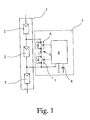
- Fig. 1 shows a solar cell 1, which has a plurality of series-connected strings 2, which in turn consist of several, not shown in detail, also connected in series solar cells.
- the provision of three strings 2 for the solar cell module 1 is purely exemplary.
- the protection via a protection circuit according to a preferred exemplary embodiment of the invention is shown for only one string 2.
- a corresponding safeguard can of course be provided for each string.
- the aim is to provide such a protection circuit, which ensures that in the case of shading the string thus secured a current bypass for this shadowed string is achieved, so that the solar cell module 1 on the one hand remains ready for use, ie one Provides power, and on the other hand damage to the shadowed string 2 is prevented.
- the protection circuit has a controlled electronic switching arrangement 3, which has a drive circuit 4 and a switching device 5.
- the switching device 5 is formed by two switching elements, namely two mutually poled MOSFETs 6, 7, which can be controlled by the drive circuit 4. Moreover, a storage capacitor 8 is provided for the drive circuit 4, so that in case of shading of the protected by the protection circuit string 2 the following sequence is made possible:
- the drive circuit 4 Due to the intrinsic power consumption of the drive circuit 4, the voltage across the storage capacitor 8 and at the gates of the MOSFETs 6, 7 decreases slowly from. Once a voltage is exceeded, in which a complete Aufsteuem the MOSFETs 6, 7 is no longer guaranteed, the drive circuit 4 turns off at least the MOSFET 7 from. Via the MOSFET 7, a voltage builds up, which in turn, as described above, limited. The Leitendphase the MOSFETs 6, 7 takes several tens of milliseconds.
- the drive circuit 4 is further designed such that it is not supplied when lighting the thus secured strings 2, so that the MOSFETs 6, 7 block.
- the MOSFETs 6, 7 In addition to the low reverse currents of the MOSFETs 6, 7 thus occur through the controlled electronic switching device 3 no losses, so that the total losses are in practice even below those of Schottky diodes.
- the protection circuit according to a preferred embodiment of the invention is essential that the controlled electrical switching device in the voltage-limited blocking phase of the remaining, so still lit strings 2 supplies, so that no external supply is required.
- the drive circuit 4 essentially comprises a Schmitt trigger, which is supplied by the drain of the MOSFET 7.
- This Schmitt trigger ensures that the MOSFETs 6, 7 are only turned on when a voltage is applied to the capacitor 8.
- the pulse-pause ratio results from the hysteresis of the Schmitt trigger and the intrinsic current consumption of the switching arrangement 3 in conjunction with the capacitance of the capacitor 8.
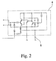
- the drive circuit 4 can be particularly simple z.
- a voltage supervisor IC such as the MAX6462 from Maxim Integrated Products.
- a simple additional wiring is required, which has a diode that protects the circuit from the regular poled operating voltage when the string is lit, and a resistor that limits the current through this diode, as long as the MOSFETs are not turned on yet.
- the diode in conjunction with the resistor at the output of the drive circuit 4 limits the voltage across the MOSFETs 6, 7, while the voltage across the capacitor 8 only builds up.
- the drive circuit 4 is a total of essentially a comparator circuit, which may be constructed in detail as well as from Fig. 2 seen.
- This circuit essentially represents a discrete simulation of the aforementioned voltage supervisor IC with the additional circuit also mentioned above.
- a solar cell module usually has a plurality of strings A, B,..., X connected in series, to which at least a switching arrangement 100 is assigned as a protective device.
- strings A, B are shown explicitly, while string X is only indicated by dots and should represent that basically any number of strings can be connected in series.
- Each string A - X consists of several series-connected solar cells 1 - n.
- each string A - X as a protective device to a MOSFET 10 and a DC / DC converter 20 which is connected via an energy storage 30 with a drive circuit 40 in connection.
- a MOSFET 10 is in each case arranged parallel to a string A - X and is connected via its gate to the drive circuit 40. All strings A - X are combined to form a solar cell module and assigned to a converter UM.
- FIG. 4 shows, according to the third preferred embodiment of the invention, two of the strings A - X, namely in each case the two strings A and B and C and D together assigned to a protective device.
- Each solar cell row A and B or C and D has a MOSFET 10 connected in parallel.
- the two MOSFETs 10 are each connected to a common drive circuit 40 via their gate, the supply of the drive circuit 40 being effected by the two DC / DC converters 20, each associated with a string A - X, which are parallel to the series connection of the strings A - X. are connected, wherein one of the DC / DC converter 20, an energy storage 30 is assigned.
- the common protection device for two of the strings A - X is alternately supplied alternately from the voltage applied across a MOSFET 10, because there are two MOSFETs 10 per protection device.
- a sufficient voltage can be obtained from the sum of the forward voltages of the parasitic diodes of the MOSFETs 10 in order to use them for converting and driving the MOSFETs 10. All strings A - X are also combined to form a solar cell module and assigned to a converter UM.
- the DC / DC converter 20 off Fig. 3 can be formed in detail.
- the DC / DC converter 20 which converts the voltage resulting from the shadowing of a string A - X into the internal diode of the MOSFET 10 into a voltage suitable for driving the MOSFET 10, should operate with input voltages below 0.7 V to bypass Ensure function.
- z. B. serve with a germanium transistor 50 constructed Meissner oscillator whose transformer contains a third winding.
- Meissner oscillator reference may be made to the textbook by U. Tietze and Ch. Schenk "Halbleiter-Scenstechnik", 9th edition, p. 461 f.
- a silicon diode 60 arranged antiparallel to the base-emitter path of the transistor 50 serves to protect the transistor 50 against the inverse input voltage present when the string A - X is illuminated.
- the drive circuit 40 consists essentially of a Schmitt trigger which, when a specific threshold voltage is exceeded across the capacitor 30, applies this voltage to the gate of the MOSFET 10 sets and falls below this threshold voltage by a value given by the hysteresis the gate discharges.
- the Schmitt trigger ensures that the MOSFET 10 is only turned on when the capacitor 30, a voltage above the threshold voltage of the MOSFETs 10 is applied.
- the pulse-pause ratio results from the hysteresis of the Schmitt trigger and the self-current consumption of the overall circuit in conjunction with the capacitance of the capacitor 30.
- the Schmitt trigger can be realized particularly easily with a voltage supervisor IC, such as the previously mentioned MAX6462 from Maxim Integrated Products.
- a voltage supervisor IC such as the previously mentioned MAX6462 from Maxim Integrated Products.
- suitable Schmitt trigger circuits are achieved, in particular by the use of logic-level MOSFETs.
- Fig. 6 Now, an example of a drive circuit 40 can be seen in detail, as it practically corresponds to a discrete replica of a voltage supervisor IC.
- protection circuits for solar cells of a solar cell module are thus provided by the invention, which are just as unproblematic as a protective circuit with bypass diodes, but have significantly lower power losses, so that much higher currents can be hedged.
Landscapes
- Engineering & Computer Science (AREA)
- Electromagnetism (AREA)
- Sustainable Development (AREA)
- Sustainable Energy (AREA)
- Physics & Mathematics (AREA)
- Condensed Matter Physics & Semiconductors (AREA)
- Life Sciences & Earth Sciences (AREA)
- General Physics & Mathematics (AREA)
- Computer Hardware Design (AREA)
- Microelectronics & Electronic Packaging (AREA)
- Power Engineering (AREA)
- Photovoltaic Devices (AREA)
- Charge And Discharge Circuits For Batteries Or The Like (AREA)
- Protection Of Static Devices (AREA)
Description
Die Ereindung betrifft eine Schutzschaltung gemäß dem Oberbegriff des Patentansprüche 1 oder 3.The invention relates to a protective circuit according to the preamble of
Solche Schutzschaltungen zum elektrischen Anschluß an Solarzellen eines Solarzellenmoduls sind aus der
Im allgemeinen werden mehrere Solarzellen zu Solarzellenmodulen zusammengeschaltet. Dazu besteht entweder die Möglichkeit der Reihenschaltung oder die Möglichkeit der Parallelschaltung der Solarzellen im Solarzellenmodul. Durch ein Parallelschalten der Solarzellen addieren sich die einzelnen Ströme der Solarzellen zu einem Gesamtstrom. Dabei sollten die parallel geschalteten Solarzellen allerdings im wesentlichen die gleichen physikalischen Eigenschaften aufweisen, so daß sich in der Praxis das Parallelschalten von Solarzellen kaum durchgesetzt hat, insbesondere auch da eine einzelne Solarzelle bereits einen Strom von einigen Ampere liefern kann und die Ausgangsspannung einzelner Solarzellen typischerweise zu gering ist, um elektrische Geräte, wie Haushaltsgeräte, betreiben zu können.In general, several solar cells are interconnected to form solar cell modules. For this purpose, there is either the possibility of series connection or the possibility of parallel connection of the solar cells in the solar cell module. By connecting the solar cells in parallel, the individual currents of the solar cells add up to a total current. The parallel solar cells should, however, have substantially the same physical properties, so that the parallel connection of solar cells has hardly prevailed in practice, especially since a single solar cell can already supply a current of a few amperes and the output voltage of individual solar cells typically is low to operate electrical appliances, such as household appliances.
Bei der Zusammenstellung on Solarzellenmodulen aus einzelnen Solarzellen werden diese daher häufig Reihe geschaltet. Ein Problem kann sich dabei jedoch dann ergeben, wenn ein Solarzellenmodul im Betrieb partiell abgeschattet wird, also eine Solarzelle oder eine Mehrzahl von Solarzellen des Solarzellenmoduls weniger oder gar keine Sonnenbestrahlung erhält. Der Grund für eine derartig verringerte Sonnenbestrahlung kann z. B. in einer Verschmutzung der Solarzellen und/oder in Schattenwürfen von Bäumen, Gebäudeeinrichtungen oder Gebäuden selbst liegen.When putting together solar cell modules from individual solar cells, these are therefore often connected in series. However, a problem may arise when a solar cell module is partially shaded during operation, that is to say a solar cell or a plurality of solar cells of the solar cell module receives less or no solar radiation. The reason for such a reduced solar radiation can z. B. in a pollution of the solar cells and / or shadows cast by trees, building facilities or buildings themselves.
Im Gegensatz zu einer Abschaltung des Solarzellenmoduls gleichmäßig über seine gesamte Fläche, die nur zur einer Leistungsverringerung insgesamt führt, ergibt sich bei einer partiellen Abschattung folgendes Problem: Durch die in Reihe geschalteten Solarzellen des Solarzellenmoduls fließt ein gemeinsamer Strom, wobei jede einzelne Solarzelle mit ihrer jeweiligen Spannung zur Gesamtspannung des Solarzellenmoduls beiträgt. Wird nun eine Solarzelle abgeschattet, so erzeugt diese keine Spannung mehr und setzt dem Stromfluß im Solarzellenmodul praktisch eine Diode in Sperrichtung entgegen. Dies bedeutet jedoch, daß das gesamte Solarzellenmodul keinen Strom mehr liefern kann, so daß die gesamte Funktion des Solarzellenmoduls beeinträchtigt ist.In contrast to a shutdown of the solar cell module evenly over its entire surface, which leads only to a reduction in performance overall, resulting in a partial shading the following problem: the series-connected solar cells of the solar cell module, a common current flows, each individual solar cell contributes with their respective voltage to the total voltage of the solar cell module. If a solar cell is now shaded, it no longer generates any voltage and practically counteracts the current flow in the solar cell module by a diode in the reverse direction. However, this means that the entire solar cell module can no longer provide power, so that the entire function of the solar cell module is impaired.
Weiterhin gilt, daß an der abgeschatteten Solarzelle eine Spannung anliegt, die abhängig ist von der Position der abgeschatteten Solarzelle in der Reihenschaltung. Ist diese an der abgeschatteten Solarzelle anliegende Spannung größer als ihre Sperrspannung, so wird es in der Solarzelle zu einem Durchschlag und damit zu einer dauerhaften Beschädigung kommen.Furthermore, it applies that a voltage is applied to the shaded solar cell, which is dependent on the position of the shaded solar cell in the series circuit. If this voltage applied to the shaded solar cell is greater than its blocking voltage, a breakdown and thus permanent damage will occur in the solar cell.
Selbst wenn es zu keiner Beschädigung der Solarzelle durch einen Durchschlag kommen sollte, wird in einer abgeschatteten Solarzelle eine große Verlustleistung umgesetzt, so daß sich die abgeschattete Solarzelle aufheizt. Auch eine solche Aufheizung kann zu Beschädigungen an der abgeschatteten Solarzelle sowie an den ihr benachbarten Solarzellen führen.Even if there should be no damage to the solar cell by a breakdown, a large power loss is implemented in a shaded solar cell, so that heats up the shaded solar cell. Such heating can also lead to damage to the shaded solar cell and to the solar cells adjacent to it.
Um die mit teilweise abgeschatteten Solarzellen verbundene Problematik vermeiden, werden Schutzeinrichtungen verwendet, im allgemeinen nämlich Bypass-Dioden, die antiparallel zu den Solarzellen geschaltet werden. Auf diese Weise wird erreicht, daß eine abgeschattete Solarzelle zwar keinen Anteil mehr zur Gesamtspannung des Solarzellenmoduls leistet, der Stromfluß jedoch trotzdem erhalten bleibt. Das Solarzellenmodul zeigt somit lediglich eine verminderte Betriebsspannung, fällt jedoch nicht vollständig aus. Außerdem wird in der abgeschatteten Solarzelle keine Leistung mehr umgesetzt, so daß eine Beschädigung der abgeschatteten Solarzelle vermieden werden kann.In order to avoid the problems associated with partially shaded solar cells, protective devices are used, generally bypass diodes which are connected in anti-parallel to the solar cells. In this way, it is achieved that a shaded solar cell does not contribute more to the total voltage of the solar cell module, but the current flow is still maintained. The solar cell module thus only shows a reduced operating voltage, but does not completely fail. In addition, no power is converted in the shaded solar cell, so that damage to the shaded solar cell can be avoided.
Grundsätzlich könnte jeder Solarzelle eines Solarzellenmoduls genau eine Bypass-Diode zugeordnet sein. Häufig jedoch wird so vorgegangen, daß eine Mehrzahl hintereinander geschalteter Solarzellen, also ein sogenannter String von Solarzellen, jeweils durch eine gemeinsame Bypass-Diode abgesichert wird.In principle, each solar cell of a solar cell module could be assigned exactly one bypass diode. Frequently, however, the procedure is such that a plurality of solar cells connected in series, that is to say a so-called string of solar cells, are each protected by a common bypass diode.
Schutzschaltungen zum elektrischen Anschluß an Solarzellen eines Solarzellenmoduls weisen somit im allgemeinen wenigstens eine Bypass-Diode, häufig eine Mehrzahl von Bypass-Dioden auf. Damit ist jedoch das Problem verbunden, daß die zum elektrischen Anschluß von Solarzellen eines Solarzellenmoduls verwendeten Schutzschaltungen durch die in den Bypass-Dioden umgesetzte Leistung stark erwärmt werden, was unter verschiedenen Aspekten nachteilig ist.Protective circuits for the electrical connection to solar cells of a solar cell module thus generally have at least one bypass diode, often a plurality of bypass diodes. However, this involves the problem that the protective circuits used for the electrical connection of solar cells of a solar cell module are strongly heated by the power converted in the bypass diodes, which is disadvantageous in various aspects.
In der
Weiterhin ist aus der
Schließlich ist in der
Es ist die Aufgabe der Erfindung, eine derartige Schutzschaltung zum elektrischen Anschluß an Solarzellen eines Solarzellenmoduls anzugeben, die sich im Betrieb nur gering erwärmt.It is the object of the invention to provide such a protective circuit for the electrical connection to solar cells of a solar cell module, which heats only slightly during operation.
Die zuvor genannte Aufgabe ist durch die Gegenstände der unabhängigen Ansprüche gelöst.The above object is solved by the subject matters of the independent claims.
Erfindungsgemäß ist also vorgesehen, daß zur Vermeidung der oben beschriebenen, mit teilweise abgeschatteten Solarzellen verbundenen Problematik als Schutzeinrichtung eine gesteuerte elektronische Schaltanordnung verwendet wird, so daß die Verwendung von Bypass-Dioden reduziert oder ganz vermieden werden kann. Durch den Ersatz von Bypass-Dioden durch eine gesteuerte elektronische Schaltanordnung, die zu den Bypass-Dioden funktional im wesentlichen gleichwirkend ist, kann eine Verringerung der Erwärmung der Schaltanordnung erzielt werden, wie nachfolgend ausgeführt.The invention thus provides that in order to avoid the problems described above associated with partially shaded solar cells as a protective device, a controlled electronic switching device is used, so that the use of bypass diodes can be reduced or avoided altogether. By replacing by-pass diodes with a controlled electronic circuitry that is functionally substantially equivalent to the bypass diodes, a reduction in the heating of the circuitry can be achieved, as set forth below.
Diese funktionale Gleichwirkung zu den aus dem Stand der Technik bekannten Bypass-Dioden kann nun auf unterschiedliche Arten und Weisen erzielt werden. Erfindungsgemäß ist dazu vorgesehen, daß die gesteuerte elektronische Schaltanordnung eine Ansteuerschalung und eine von der Ansteuerschaltung ansteuerbare Schalteinrichtung aufweist, wobei die Schalteinrichtung parallel zu wenigstens einer Solarzelle, vorzugsweise parallel zu einem String von Solarzellen, geschaltet ist und im Falle einer Abschattung einer der Solarzellen, zu der sie parallel geschaltet ist, von der Ansteuerschaltung wenigstens zeitweise aufgesteuert wird, so daß ein Strom-Bypass für die abgeschattete Solarzelle erzielt wird.This functional equality with the known from the prior art bypass diodes can now be achieved in different ways. According to the invention, it is provided that the controlled electronic switching arrangement has a drive circuit and a switching device which can be controlled by the drive circuit, the switching device being connected in parallel to at least one solar cell, preferably parallel to a string of solar cells, and in the case of shading of one of the solar cells it is connected in parallel, is at least temporarily turned on by the drive circuit, so that a current bypass for the shaded solar cell is achieved.
Entsprechende Schalteinrichtungen lassen sich auf verschiedene Arten realisieren. Gemäß einer Ansgestaltung der Erfindung ist jedoch vorgesehen, daß die Schalteinrichtung zwei in Reihe geschaltete und von der Ansteuerschaltung angesteuerte elektrische oder elektronische Schaltelemente aufweist. Erfindungsgemäß ist dabei vorgesehen, daß als Schaltelemente zwei gegeneinander gepolte Transistoren, vorzugsweise zwei MOSFETs, vorgesehen sind. Weiterhin gilt, daß gemäß einer bevorzugten Weiterbildung der Erfindung vorgesehen ist, daß die Stromversorgung der Ansteuerschaltung über den von den nicht abgeschatteten Solarzellen des Solarzellenmoduls erzeugten Strom erfolgt, wobei gemäß einer bevorzugten Weiterbildung der Erfindung insbesondere vorgesehen ist, daß die Ansteuerschaltung mit einem Speicherkondensator versehen ist.Corresponding switching devices can be realized in various ways. According to an Ansgestaltung of the invention, however, it is provided that the switching device has two series-connected and driven by the drive circuit electrical or electronic switching elements. According to the invention it is provided that two mutually poled transistors, preferably two MOSFETs are provided as switching elements. Furthermore, according to a preferred embodiment of the invention, it is provided that the power supply of the drive circuit via the power generated by the unshaded solar cells of the solar cell module current is provided according to a preferred embodiment of the invention, in particular, that the drive circuit is provided with a storage capacitor ,
Gemäß der Erfindung ist alternativ vorgesehen, daß als Schutzeinrichtung eine gesteuerte elektronische Schaltungsanordnung vorgesehen ist, die für wenigstens einen String von Solarzellen wenigstens einen Transistor und wenigstens einen parallel dazu geschalteten DC/DC-Wandler aufweist, welcher über einen Energiespeicher mit einer Ansteuerschaltung in Verbindung steht Bei einer solchen Ausbildung ist besonders vorteilhaft, daß die Schutzeinrichtung wenige preisgünstige MOSFETs mit geringem Platzbedarf aufweist, weil mit Hilfe eines Spannungswandlers bereits aus der geringen Flußspannung der parasitären Diode des MOSFET die Spannung erzeugt wird, die zu dessen Ansteuerung erforderlich ist.According to the invention, it is alternatively provided that as a protective device a controlled electronic circuit arrangement is provided, which has at least one transistor and at least one parallel connected DC / DC converter for at least one string of solar cells, which is connected via an energy store with a drive circuit With such a design is particularly advantageous that the protective device has a few low-cost MOSFETs with a small footprint, because with the help of a voltage converter already from the low Flußspannung the parasitic diode of the MOSFET, the voltage is generated, which is required for its control.
Weiterhin ist besonders vorteilhaft, wenn die Spannungswandlung durch die Integration einer Schutzeinrichtung in wenigstens zwei Strings von Solarzellen eines Solarzellenmodnls erfolgt. Einerseits ist es so möglich, daß sich die Schutzeinrichtung wechselweise aus der Spannung, die über einem MOSFET ansteht, ausreichend versorgt wird, weil mehrere MOSFETs vorhanden sind. Andererseits kann bei Abschattung aller zu einem String gehörenden Solarzellen aus der Summe der Flußspannungen der parasitären Dioden der MOSFETs eine ausreichende Spannung gewonnen werden, um diese zur Wandlung und Ansteuerung der MOSFETs zu verwenden. Zudem ist es vorteilhaft, daß die maximale, in Rückwärtsrichtung auftretende Spannung je Schutzeinrichtung auf die Flußspannung einer Siliziumdiode begrenzt ist, was das Risiko des kompletten Ausfalls der Versorgung bei unzureichender Beleuchtung der in Betrieb verbliebenen Solarzellen z. B. bei diffusem Licht minimiert.Furthermore, it is particularly advantageous if the voltage conversion takes place through the integration of a protective device into at least two strings of solar cells of a solar cell module. On the one hand, it is possible that the protection device is alternately supplied alternately from the voltage that is present across a MOSFET, because there are several MOSFETs. On the other hand, with shading of all the solar cells belonging to a string, a sufficient voltage can be obtained from the sum of the forward voltages of the parasitic diodes of the MOSFETs in order to use these for the conversion and control of the MOSFETs. Moreover, it is advantageous that the maximum, occurring in the reverse direction voltage per protective device is limited to the forward voltage of a silicon diode, which increases the risk of complete failure of the supply in case of insufficient illumination of the solar cells remaining in operation z. B. minimized in diffused light.
Schließlich ist bei allen zuvor genannten Ausgestaltung von Schutzschaltungen für Solarzellen eines Solarzellenmoduls gemäß eines Beipiels, das nicht Teil der beanspruchten Erfindung ist vorgesehen, daß ein Überspannungsschutzelement zum Schutz der Schutzschaltung sowie der Solarzellen vor Überspannungen, z.B. durch einen benachbarten Blitzeinschlag, verwendet wird.Finally, in all the above-mentioned configuration of solar cell protection circuits of a solar cell module according to an example not part of the claimed invention, it is provided that an overvoltage protection element for protecting the protection circuit and the solar cells from overvoltages, e.g. by an adjacent lightning strike.
Im einzelnen gibt es nun eine Vielzahl von Möglichkeiten, die erfindungsgemäßen Schutzschaltungen auszugestalten und weiterzubilden. Dazu wird auf die Unteransprüche sowie auf die nachfolgende detaillierte Beschreibung eines bevorzugten Ausführungsbeispiels der Erfindung verwiesen. In der Zeichnung zeigt
- Fig. 1
- schematisch eine Schutzschaltung gemäß einem ersten bevorzugten Ausführungsbeispiel der Erfindung,
- Fig. 2
- den Aufbau der Ansteuerschaltung aus
Fig. 1 im einzelnen, - Fig. 3
- schematisch eine Schutzschaltung gemäß einem zweiten bevorzugten Ausführungsbeispiel,
- Fig. 4
- schematisch eine Schutzschaltung gemäß einem dritten bevorzugten Ausführungsbeispiel,
- Fig. 5
- den Aufbau eines DC/DC-Wandlers aus den
Fig. 3 bzw. 4 im einzelnen und - Fig. 6
- den Aufbau einer Ansteuerschaltung aus den
Fig. 3 bzw. 4 im einzelnen.
- Fig. 1
- schematically a protection circuit according to a first preferred embodiment of the invention,
- Fig. 2
- the structure of the drive circuit
Fig. 1 in detail, - Fig. 3
- schematically a protection circuit according to a second preferred embodiment,
- Fig. 4
- schematically a protection circuit according to a third preferred embodiment,
- Fig. 5
- the structure of a DC / DC converter from the
Fig. 3 or 4 in detail and - Fig. 6
- the structure of a drive circuit of the
Fig. 3 or 4 in detail.
Wie zuvor schon ausgeführt, ist es das Ziel, eine derartige Schutzschaltung anzugeben, die gewährleistet, daß im Falle einer Abschattung des damit abgesicherten Strings ein Strom-Bypass für diesen abgeschatteten String erzielt wird, so daß das Solarzellenmodul 1 einerseits weiterhin einsatzbereit bleibt, also einen Strom liefert, und andererseits eine Beschädigung des abgeschatteten Strings 2 verhindert wird. Dazu weist die Schutzschaltung eine gesteuerte elektronische Schaltanordnung 3 auf, die über eine Ansteuerschaltung 4 sowie eine Schalteinrichtung 5 verfügt.As stated above, the aim is to provide such a protection circuit, which ensures that in the case of shading the string thus secured a current bypass for this shadowed string is achieved, so that the
Die Schalteinrichtung 5 wird von zwei Schaltelementen gebildet, nämlich von zwei gegeneinander gepolten MOSFETs 6, 7, die von der Ansteuerschaltung 4 ansteuerbar sind. Im übrigen ist für die Ansteuerschaltung 4 ein Speicherkondensator 8 vorgesehen, so daß im Falle einer Abschattung des durch die Schutzschaltung abgesicherten Strings 2 folgender Ablauf ermöglicht wird:The switching device 5 is formed by two switching elements, namely two mutually poled
Bei Abschattung des abgesicherten Strings 2 und weiterer Beleuchtung der verbleibenden Strings 2 des Solarzellenmoduls 1 baut sich über den unteren, sperrend wirkenden MOSFET 7 aufgrund der parasitären Diode des oberen MOSFETs 6 eine Spannung auf. Die Ansteuerschaltung 4 ist nun derart ausgelegt, daß sie diese Spannung durch teilweises Aufsteuern wenigstens des MOSFETs 7 auf ca. 20 V begrenzt, so daß eine Beschädigung des abgesicherten Strings 2 vermieden wird. In dieser Phase lädt sich der Speicherkondensator 8 strombegrenzt aus der Spannung über den MOSFET 7 auf. Sobald der Speicherkondensator 8 auf ca. 15 V aufgeladen ist, werden die MOSFETs 6, 7 vollständig aufgesteuert, wodurch die über den MOSFETs 6, 7 anliegende Spannung zusammenbricht. Vom Auftreten der anfänglichen Sperrspannung bis zu diesem Zeitpunkt des Zusammenbrechens der Spannung vergehen nur wenige Mikrosekunden.When shading the fused
Durch den Eigenstromverbrauch der Ansteuerschaltung 4 sinkt die Spannung über dem Speicherkondensator 8 und an den Gates der MOSFETs 6, 7 langsam ab. Sobald eine Spannung unterschritten wird, bei der ein vollständige Aufsteuem der MOSFETs 6, 7 nicht mehr gewährleistet ist, schaltet die Ansteuerschaltung 4 wenigstens den MOSFET 7 ab. Über den MOSFET 7 baut sich dann eine Spannung auf, die wiederum, wie oben beschrieben, begrenzt wird. Die Leitendphase der MOSFETs 6, 7 dauert mehrere zehn Millisekunden. Aufgrund der verglichen zur Leitendphase sehr kurzen spannungsbegrenzten Sperrphase fallen die momentan hohen Verlustleistungen über den MOSFETs 6, 7 während der Sperrphasen damit gegenüber den Leitendverlusten kaum ins Gewicht, so daß insgesamt Verluste deutlich unter denen einer Schottky-Diode erreicht wird.Due to the intrinsic power consumption of the
Die Ansteuerschaltung 4 ist weiterhin derart ausgelegt, daß sie bei Beleuchtung des damit abgesicherten Strings 2 nicht versorgt wird, so daß die MOSFETs 6, 7 sperren. Außer den geringen Sperrströmen der MOSFETs 6, 7 treten somit durch die gesteuerte elektronische Schaltanordnung 3 keinerlei Verluste auf, so daß die Gesamtverluste in der Praxis sogar unter denen von Schottky-Dioden liegen. Darüber hinaus ist bei der vorliegend beschriebenen Schutzschaltung gemäß einem bevorzugten Ausführungsbeispiel der Erfmdung wesentlich, daß sich die gesteuerte elektrische Schaltanordnung in der spannungsbegrenzten Sperrphase aus den verbleibenden, also noch beleuchteten Strings 2 versorgt, so daß keine Fremdversorgung erforderlich ist.The
Um die oben genannte Funktionalität zu ermöglichen, weist die Ansteuerschaltung 4 im wesentlichen einen Schmitt-Trigger auf, der vom Drain des MOSFETs 7 versorgt wird. Dieser Schmitt-Trigger sorgt dafür, daß die MOSFETs 6, 7 nur dann aufgesteuert werden, wenn am Kondensator 8 eine Spannung anliegt. Das Puls-Pausen-Verhältnis ergibt sich aus der Hysterese des Schmitt-Triggers und dem Eigenstromverbrauch der Schaltanordnung 3 in Verbindung mit der Kapazität des Kondensators 8.To enable the above-mentioned functionality, the
Die Ansteuerschaltung 4 läßt sich besonders einfach z. B. mit einem Voltage-Supervisor-IC verwirklichen, wie dem MAX6462 von Maxim Integrated Products. Bei Verwendung eines solchen Voltage-Supervisor-IC ist lediglich eine einfache zusätzliche Beschaltung erforderlich, die eine Diode aufweist, die die Schaltung vor der regulären gepolten Betriebsspannung bei beleuchtetem String schützt, und einem Widerstand, der den Strom durch diese Diode begrenzt, solange die MOSFETs noch nicht durchgeschaltet sind. Die Diode in Verbindung mit dem Widerstand am Ausgang der Ansteuerschaltung 4 begrenzt die Spannung über die MOSFETs 6, 7, während sich die Spannung über den Kondensator 8 erst aufbaut.The
Damit stellt die Ansteuerschaltung 4 insgesamt im wesentlichen eine Komparatorschaltung dar, die im einzelnen auch so aufgebaut sein kann, wie aus
Im folgenden werden ein zweites und ein drittes bevorzugtes Ausführungsbeispiel der Erfindung beschrieben, die einen bzw. zwei DC/DC-Wandler aufweisen.In the following, a second and a third preferred embodiment of the invention will be described, which have one or two DC / DC converter.
Wie aus den
Wie insbesondere aus
Wie insbesondere aus
Aus
Die Ansteuerschaltung 40 besteht im einfachsten Fall im wesentlichen aus einem Schmitt-Trigger, der bei Überschreiten einer bestimmten Schwellspannung über den Kondensator 30 diese Spannung auf das Gate des MOSFETs 10 legt und bei Unterschreitung dieser Schwellspannung um einen durch die Hysterese gegebenen Wert das Gate entlädt. Der Schmitt-Trigger sorgt dafür, daß der MOSFET 10 nur dann aufgesteuert wird, wenn am Kondensator 30 eine Spannung oberhalb der Schwellspannung der MOSFETs 10 anliegt. Das Puls-Pausenverhältnis ergibt sich aus der Hysterese des Schmitt-Triggers und dem Eigenstromverbrauch der Gesamtschaltung in Verbindung mit der Kapazität des Kondensators 30.In the simplest case, the
Ähnlich wie die weiter oben beschriebene Ansteuerschaltung 4 aus
Im Ergebnis werden durch die Erfindung damit Schutzschaltungen für Solarzellen eines Solarzellenmoduls bereitgestellt, die genauso unproblematisch einsetzbar sind wie eine Schutzschaltung mit Bypass-Dioden, jedoch wesentlich geringere Verlustleistungen aufweisen, so daß wesentlich höhere Ströme abgesichert werden können.As a result, protection circuits for solar cells of a solar cell module are thus provided by the invention, which are just as unproblematic as a protective circuit with bypass diodes, but have significantly lower power losses, so that much higher currents can be hedged.
Claims (10)
- Protective circuit for the electrical connection of at least one solar cell of a solar cell module (1), with a protective device having a controlled electronic switching arrangement (3, 100), wherein
the controlled electronic switching arrangement (3, 100) has an actuating circuit (4, 40) and a switching device (5, 10) actuated by the actuating circuit (4, 40), the switching device (5, 10) is hooked up in parallel with at least one solar cell and in event of a shadowing of the solar cell it is at least temporarily actuated by the actuating circuit (4, 40) so that a current bypass is achieved for the shadowed solar cell, characterized in that the protective device in the case of the shadowed solar cell acts as a current bypass for the shadowed solar cell in parallel with the shadowed solar cell,
the switching device (5) has two series-switched electrical or electronic switch elements (6, 7) actuated by the actuating circuit (4) and two opposite-poled transistors are provided as switch elements (6, 7). - Protective circuit according to claim 1, characterized in that the opposite-poled transistors are MOSFETs.
- Protective circuit for the electrical connection of at least one solar cell of a solar cell module (1), with a protective device having a controlled electronic switching arrangement (3, 100), wherein
the controlled electronic switching arrangement (3, 100) has an actuating circuit (4, 40) and a switching device (5, 10) actuated by the actuating circuit (4, 40) and the switching device (5, 10) is hooked up in parallel with at least one solar cell and in event of a shadowing of the solar cell it is at least temporarily actuated by the actuating circuit (4, 40) so that a current bypass is achieved for the shadowed solar cell, characterized in that the protective device in the case of the shadowed solar cell acts as a current bypass for the shadowed solar cell in parallel with the shadowed solar cell, and the protective device has at least one transistor (10) and at least one DC/DC converter (20) hooked up in parallel with it, which is in communication with the actuating circuit (40) across an energy accumulator (30). - Protective circuit according to claim 3, characterized in that a MOSFET is provided as the transistor (10).
- Protective circuit according to claim 3 or 4, characterized in that several strings (A-X) of solar cells are associated jointly with a protective device, having one parallel switched transistor (10) for each string (A-X), which communicates by its respective gate with an actuating circuit (40).
- Protective circuit according to claim 5, characterized in that the power supply of the actuating circuit (40) comes from a respective DC/DC converter (20) for each string (A-X), the DC/DC converters (20) being switched in parallel with the series circuit of the strings (A-X).
- Protective circuit according to claim 6, characterized in that at least one of the DC/DC converters (20) is associated with an energy accumulator (30).
- Protective circuit according to one of claims 1 to 7, characterized in that the actuating circuit (40) of the electronic switching arrangement has a microcontroller.
- Protective circuit according to one of claims 1 to 8, characterized in that the power supply of the actuating circuit (4) comes from the current generated by the nonshadowed solar cells of the solar cell module (1).
- Protective circuit according to one of claims 1 to 9, characterized in that a storage capacitor (8, 30) is provided for the actuating circuit (4).
Applications Claiming Priority (4)
| Application Number | Priority Date | Filing Date | Title |
|---|---|---|---|
| DE102005003720 | 2005-01-26 | ||
| DE102005012213A DE102005012213B4 (en) | 2005-01-26 | 2005-03-15 | Connected circuit |
| DE102005018463 | 2005-04-20 | ||
| PCT/EP2006/000599 WO2006079503A2 (en) | 2005-01-26 | 2006-01-24 | Protective circuit with current bypass for solar cell module |
Publications (3)
| Publication Number | Publication Date |
|---|---|
| EP1849189A2 EP1849189A2 (en) | 2007-10-31 |
| EP1849189B1 EP1849189B1 (en) | 2012-09-05 |
| EP1849189B9 true EP1849189B9 (en) | 2012-12-26 |
Family
ID=36694489
Family Applications (1)
| Application Number | Title | Priority Date | Filing Date |
|---|---|---|---|
| EP20060701624 Active EP1849189B9 (en) | 2005-01-26 | 2006-01-24 | Protective circuit with current bypass for solar cell module |
Country Status (4)
| Country | Link |
|---|---|
| US (2) | US7864497B2 (en) |
| EP (1) | EP1849189B9 (en) |
| ES (1) | ES2393647T3 (en) |
| WO (1) | WO2006079503A2 (en) |
Families Citing this family (103)
| Publication number | Priority date | Publication date | Assignee | Title |
|---|---|---|---|---|
| ES2393647T3 (en) * | 2005-01-26 | 2012-12-26 | Günther Spelsberg GmbH & Co. KG | Protection circuit with current bypass for a solar cell module |
| US11881814B2 (en) | 2005-12-05 | 2024-01-23 | Solaredge Technologies Ltd. | Testing of a photovoltaic panel |
| US10693415B2 (en) | 2007-12-05 | 2020-06-23 | Solaredge Technologies Ltd. | Testing of a photovoltaic panel |
| US8947194B2 (en) | 2009-05-26 | 2015-02-03 | Solaredge Technologies Ltd. | Theft detection and prevention in a power generation system |
| US11855231B2 (en) | 2006-12-06 | 2023-12-26 | Solaredge Technologies Ltd. | Distributed power harvesting systems using DC power sources |
| US11309832B2 (en) | 2006-12-06 | 2022-04-19 | Solaredge Technologies Ltd. | Distributed power harvesting systems using DC power sources |
| US9112379B2 (en) | 2006-12-06 | 2015-08-18 | Solaredge Technologies Ltd. | Pairing of components in a direct current distributed power generation system |
| US8013472B2 (en) | 2006-12-06 | 2011-09-06 | Solaredge, Ltd. | Method for distributed power harvesting using DC power sources |
| US9130401B2 (en) | 2006-12-06 | 2015-09-08 | Solaredge Technologies Ltd. | Distributed power harvesting systems using DC power sources |
| US11687112B2 (en) | 2006-12-06 | 2023-06-27 | Solaredge Technologies Ltd. | Distributed power harvesting systems using DC power sources |
| US8473250B2 (en) | 2006-12-06 | 2013-06-25 | Solaredge, Ltd. | Monitoring of distributed power harvesting systems using DC power sources |
| US8816535B2 (en) | 2007-10-10 | 2014-08-26 | Solaredge Technologies, Ltd. | System and method for protection during inverter shutdown in distributed power installations |
| US11888387B2 (en) | 2006-12-06 | 2024-01-30 | Solaredge Technologies Ltd. | Safety mechanisms, wake up and shutdown methods in distributed power installations |
| US11728768B2 (en) | 2006-12-06 | 2023-08-15 | Solaredge Technologies Ltd. | Pairing of components in a direct current distributed power generation system |
| US9088178B2 (en) | 2006-12-06 | 2015-07-21 | Solaredge Technologies Ltd | Distributed power harvesting systems using DC power sources |
| US8319483B2 (en) | 2007-08-06 | 2012-11-27 | Solaredge Technologies Ltd. | Digital average input current control in power converter |
| US8319471B2 (en) | 2006-12-06 | 2012-11-27 | Solaredge, Ltd. | Battery power delivery module |
| US8384243B2 (en) | 2007-12-04 | 2013-02-26 | Solaredge Technologies Ltd. | Distributed power harvesting systems using DC power sources |
| US11735910B2 (en) | 2006-12-06 | 2023-08-22 | Solaredge Technologies Ltd. | Distributed power system using direct current power sources |
| US11296650B2 (en) | 2006-12-06 | 2022-04-05 | Solaredge Technologies Ltd. | System and method for protection during inverter shutdown in distributed power installations |
| US8618692B2 (en) | 2007-12-04 | 2013-12-31 | Solaredge Technologies Ltd. | Distributed power system using direct current power sources |
| US11569659B2 (en) | 2006-12-06 | 2023-01-31 | Solaredge Technologies Ltd. | Distributed power harvesting systems using DC power sources |
| US8963369B2 (en) | 2007-12-04 | 2015-02-24 | Solaredge Technologies Ltd. | Distributed power harvesting systems using DC power sources |
| US20090014050A1 (en) * | 2007-07-13 | 2009-01-15 | Peter Haaf | Solar module system and method using transistors for bypass |
| DE102008004675B3 (en) * | 2007-10-12 | 2009-03-05 | Fraunhofer-Gesellschaft zur Förderung der angewandten Forschung e.V. | Controllable switching device for solar module, has control provided to control controllable switching unit to switch switching unit in one of switch conditions using output of solar module or input at output terminal |
| EP2220734B1 (en) * | 2007-11-14 | 2020-01-22 | Renergyx Pty Limited | Electrical energy and distribution system |
| WO2009072076A2 (en) | 2007-12-05 | 2009-06-11 | Solaredge Technologies Ltd. | Current sensing on a mosfet |
| US8289742B2 (en) | 2007-12-05 | 2012-10-16 | Solaredge Ltd. | Parallel connected inverters |
| US11264947B2 (en) | 2007-12-05 | 2022-03-01 | Solaredge Technologies Ltd. | Testing of a photovoltaic panel |
| US9291696B2 (en) | 2007-12-05 | 2016-03-22 | Solaredge Technologies Ltd. | Photovoltaic system power tracking method |
| CN101933209B (en) | 2007-12-05 | 2015-10-21 | 太阳能安吉有限公司 | Release mechanism in distributed electrical power apparatus, to wake up and method for closing |
| US20090184746A1 (en) * | 2008-01-22 | 2009-07-23 | Microsemi Corporation | Low Voltage Drop Unidirectional Electronic Valve |
| US8111052B2 (en) | 2008-03-24 | 2012-02-07 | Solaredge Technologies Ltd. | Zero voltage switching |
| DE102008021654B3 (en) * | 2008-04-30 | 2009-12-10 | Insta Elektro Gmbh | Photovoltaic system operating method, involves analyzing temporal lapse of voltage value to determine operational voltage fluctuations and voltage modulations for data transfer from internal control unit to central control unit |
| EP2294669B8 (en) | 2008-05-05 | 2016-12-07 | Solaredge Technologies Ltd. | Direct current power combiner |
| SG160241A1 (en) * | 2008-09-15 | 2010-04-29 | Alternative Energy Technology | Photovoltaic cell circuit |
| US8791598B2 (en) * | 2008-12-21 | 2014-07-29 | NavSemi Energy Private Ltd. | System and method for selectively controlling a solar panel in segments |
| CN102422429B (en) | 2009-05-22 | 2014-08-06 | 太阳能安吉科技有限公司 | Electrically isolated heat dissipating junction box |
| US8169252B2 (en) * | 2009-07-09 | 2012-05-01 | Microsemi Corporation | Low voltage drop closed loop unidirectional electronic valve |
| US8791602B2 (en) * | 2009-08-17 | 2014-07-29 | NavSemi Energy Private Ltd. | System and method for controlling a solar panel output |
| DE102009042084A1 (en) * | 2009-09-18 | 2011-06-22 | Gehrlicher Solar AG, 85609 | Low-maintenance electronic component to prevent backflow while protecting against overcurrents in photovoltaic systems |
| US8263920B2 (en) * | 2009-09-30 | 2012-09-11 | The Boeing Company | Diodeless terrestrial photovoltaic solar power array |
| US9324885B2 (en) | 2009-10-02 | 2016-04-26 | Tigo Energy, Inc. | Systems and methods to provide enhanced diode bypass paths |
| DE102009044695A1 (en) * | 2009-11-27 | 2011-06-01 | Müller, Ingo, Dr. | Solar module, modular switch, solar cable, busbar, multi-contact connector |
| US8710699B2 (en) | 2009-12-01 | 2014-04-29 | Solaredge Technologies Ltd. | Dual use photovoltaic system |
| US8766696B2 (en) | 2010-01-27 | 2014-07-01 | Solaredge Technologies Ltd. | Fast voltage level shifter circuit |
| US9425783B2 (en) | 2010-03-15 | 2016-08-23 | Tigo Energy, Inc. | Systems and methods to provide enhanced diode bypass paths |
| KR101078799B1 (en) | 2010-03-23 | 2011-11-02 | 엘지전자 주식회사 | Photovoltaic power generation system |
| EP2564487A4 (en) | 2010-04-27 | 2015-10-28 | Navsemi Energy Private Ltd | Method and apparatus for controlling a solar panel output in charging a battery |
| IT1400921B1 (en) | 2010-05-14 | 2013-07-02 | St Microelectronics Srl | BY-PASS DIODE OR SWITCH MADE WITH A LOW RESISTANCE CONDUCTING MOSFET AND ITS SELF-POWERED CONTROL CIRCUIT |
| DE102010023549B4 (en) * | 2010-06-03 | 2016-03-24 | Dmos Gmbh | Photovoltaic generator with circuit system and method for protecting photovoltaic modules |
| EP2395550B1 (en) * | 2010-06-09 | 2013-10-09 | SMA Solar Technology AG | Method for recognising and evaluating shadowing |
| DE102010036816A1 (en) * | 2010-08-03 | 2012-02-09 | Newtos Ag | Method and device for monitoring and controlling a photovoltaic system |
| US10615743B2 (en) * | 2010-08-24 | 2020-04-07 | David Crites | Active and passive monitoring system for installed photovoltaic strings, substrings, and modules |
| US20120049855A1 (en) * | 2010-08-24 | 2012-03-01 | Crites David E | Dark IV monitoring system for photovoltaic installations |
| US10673229B2 (en) | 2010-11-09 | 2020-06-02 | Solaredge Technologies Ltd. | Arc detection and prevention in a power generation system |
| US10673222B2 (en) | 2010-11-09 | 2020-06-02 | Solaredge Technologies Ltd. | Arc detection and prevention in a power generation system |
| GB2485527B (en) * | 2010-11-09 | 2012-12-19 | Solaredge Technologies Ltd | Arc detection and prevention in a power generation system |
| US10230310B2 (en) | 2016-04-05 | 2019-03-12 | Solaredge Technologies Ltd | Safety switch for photovoltaic systems |
| GB2486408A (en) | 2010-12-09 | 2012-06-20 | Solaredge Technologies Ltd | Disconnection of a string carrying direct current |
| GB2483317B (en) | 2011-01-12 | 2012-08-22 | Solaredge Technologies Ltd | Serially connected inverters |
| DE102012010083B4 (en) * | 2011-05-23 | 2023-04-27 | Microsemi Corp. | Photovoltaic safety shutdown device |
| US8570005B2 (en) | 2011-09-12 | 2013-10-29 | Solaredge Technologies Ltd. | Direct current link circuit |
| GB2498365A (en) * | 2012-01-11 | 2013-07-17 | Solaredge Technologies Ltd | Photovoltaic module |
| US9853565B2 (en) | 2012-01-30 | 2017-12-26 | Solaredge Technologies Ltd. | Maximized power in a photovoltaic distributed power system |
| GB2498790A (en) | 2012-01-30 | 2013-07-31 | Solaredge Technologies Ltd | Maximising power in a photovoltaic distributed power system |
| GB2498791A (en) | 2012-01-30 | 2013-07-31 | Solaredge Technologies Ltd | Photovoltaic panel circuitry |
| GB2499991A (en) | 2012-03-05 | 2013-09-11 | Solaredge Technologies Ltd | DC link circuit for photovoltaic array |
| EP2859650B1 (en) | 2012-05-25 | 2017-02-15 | Solaredge Technologies Ltd. | Circuit for interconnected direct current power sources |
| US10115841B2 (en) | 2012-06-04 | 2018-10-30 | Solaredge Technologies Ltd. | Integrated photovoltaic panel circuitry |
| US9105765B2 (en) | 2012-12-18 | 2015-08-11 | Enphase Energy, Inc. | Smart junction box for a photovoltaic system |
| US9548619B2 (en) | 2013-03-14 | 2017-01-17 | Solaredge Technologies Ltd. | Method and apparatus for storing and depleting energy |
| US9941813B2 (en) | 2013-03-14 | 2018-04-10 | Solaredge Technologies Ltd. | High frequency multi-level inverter |
| EP4318001A3 (en) | 2013-03-15 | 2024-05-01 | Solaredge Technologies Ltd. | Bypass mechanism |
| DE102013106808A1 (en) * | 2013-06-28 | 2014-12-31 | Sma Solar Technology Ag | Circuit arrangement for inline power supply |
| CN103888058A (en) * | 2014-03-07 | 2014-06-25 | 苏州边枫电子科技有限公司 | Over-temperature state indication type photovoltaic terminal box based on current measurement |
| CN103888060A (en) * | 2014-03-07 | 2014-06-25 | 苏州边枫电子科技有限公司 | Over-temperature state indication type photovoltaic terminal box based on semiconductor temperature measurement |
| CN103888059A (en) * | 2014-03-07 | 2014-06-25 | 苏州边枫电子科技有限公司 | Over-temperature state indication type photovoltaic terminal box based on voltage measurement |
| CN103888057A (en) * | 2014-03-07 | 2014-06-25 | 苏州边枫电子科技有限公司 | Over-temperature status indicating type photovoltaic junction box based on far infrared heat sensors |
| US9318974B2 (en) | 2014-03-26 | 2016-04-19 | Solaredge Technologies Ltd. | Multi-level inverter with flying capacitor topology |
| CN103888067A (en) * | 2014-04-03 | 2014-06-25 | 苏州边枫电子科技有限公司 | Remote monitoring type photovoltaic junction box based on Hall sensors and FM transmission |
| CN103888062A (en) * | 2014-04-03 | 2014-06-25 | 苏州边枫电子科技有限公司 | Remote monitor type photovoltaic connecting box based on current detection and electric wire carrier waves |
| CN103888061A (en) * | 2014-04-03 | 2014-06-25 | 苏州边枫电子科技有限公司 | Remote monitor type photovoltaic connecting box based on semiconductor temperature measurement and FM transmission |
| CN103888072A (en) * | 2014-04-03 | 2014-06-25 | 苏州边枫电子科技有限公司 | Remote monitoring type photovoltaic junction box based on thermistor temperature measurement and single-line communication protocol |
| CN107210698A (en) | 2014-06-19 | 2017-09-26 | 李平 | Motor, generator and direct current switch system, apparatus and method |
| US20150372279A1 (en) * | 2014-06-24 | 2015-12-24 | Turboroto Inc. | Active battery stack system and method |
| US20160079761A1 (en) * | 2014-09-15 | 2016-03-17 | The Board Of Trustees Of The University Of Illinois | System and method for power point tracking for photovoltaic cells |
| DE102015012413A1 (en) * | 2015-04-14 | 2016-10-20 | Smartexergy Wms Gmbh | Bridging device for at least one photovoltaic module |
| CN107153212B (en) | 2016-03-03 | 2023-07-28 | 太阳能安吉科技有限公司 | Method for mapping a power generation facility |
| US11081608B2 (en) | 2016-03-03 | 2021-08-03 | Solaredge Technologies Ltd. | Apparatus and method for determining an order of power devices in power generation systems |
| US10599113B2 (en) | 2016-03-03 | 2020-03-24 | Solaredge Technologies Ltd. | Apparatus and method for determining an order of power devices in power generation systems |
| DE102016105930A1 (en) * | 2016-03-31 | 2017-10-05 | Sma Solar Technology Ag | Solar module, operating procedure For a solar module and photovoltaic system |
| US11177663B2 (en) | 2016-04-05 | 2021-11-16 | Solaredge Technologies Ltd. | Chain of power devices |
| EP3291309B1 (en) * | 2016-08-29 | 2022-08-24 | Solaredge Technologies Ltd. | Safety switch for photovoltaic systems |
| US11018623B2 (en) | 2016-04-05 | 2021-05-25 | Solaredge Technologies Ltd. | Safety switch for photovoltaic systems |
| US20180013377A1 (en) * | 2016-07-11 | 2018-01-11 | International Business Machines Corporation | Mitigating the Effects on Shading in Photovoltaic Cells Using Flow Batteries |
| DE102016115295A1 (en) * | 2016-08-17 | 2018-02-22 | Sma Solar Technology Ag | Separator for a photovoltaic string |
| CN117175565A (en) * | 2017-03-29 | 2023-12-05 | 太阳能安吉科技有限公司 | Bypass circuit and method of bypassing power module in power system |
| EP3611815A1 (en) * | 2018-08-17 | 2020-02-19 | Solaredge Technologies Ltd. | Bypass circuit and method to bypass power modules in power system |
| EP3709491A1 (en) * | 2019-03-12 | 2020-09-16 | ABB Schweiz AG | A multi-channel inverter for a photovoltaic apparatus |
| WO2020219995A1 (en) * | 2019-04-25 | 2020-10-29 | Aerovironment | System and method for solar cell array diagnostics in high altitude long endurance aircraft |
| US11855451B2 (en) * | 2020-09-25 | 2023-12-26 | Analog Devices International Unlimited Company | Bootstrapped line-protector CMOS switch |
| CN113644876B (en) * | 2021-08-12 | 2023-11-24 | 阳光新能源开发股份有限公司 | Photovoltaic power generation system and protection circuit of photovoltaic module |
Family Cites Families (10)
| Publication number | Priority date | Publication date | Assignee | Title |
|---|---|---|---|---|
| US3600599A (en) * | 1968-10-03 | 1971-08-17 | Trw Inc | Shunt regulation electric power system |
| US5367310A (en) * | 1991-10-11 | 1994-11-22 | Southwest Research Institute | Fiber optic antenna radiation efficiency tuner |
| JP2666754B2 (en) | 1994-12-19 | 1997-10-22 | 日本電気株式会社 | Power supply method in solar cell power supply |
| JP2000174308A (en) * | 1998-12-01 | 2000-06-23 | Toshiba Corp | Solar battery power generation module |
| DE19904561C1 (en) | 1999-02-04 | 2000-08-24 | Rossendorf Forschzent | Maximum power point control method for solar generator uses current characteristic for sensor of similar type and charge for calculation of power characteristic used for providing setting parameter for solar generator |
| DE19916742C1 (en) | 1999-04-13 | 2000-08-24 | Angew Solarenergie Ase Gmbh | Solar cell current generation circuit has bypass diodes across each solar cell chain connected in series and bridged in groups by further diodes |
| US6246219B1 (en) * | 2000-03-24 | 2001-06-12 | The Boeing Company | String switching apparatus and associated method for controllably connecting the output of a solar array string to a respective power bus |
| DE10222621A1 (en) * | 2002-05-17 | 2003-11-27 | Josef Steger | Process and circuit to control and regulated a photovoltaic device assembly for solar energy has controlled bypass for each cell to ensure maximum power operation |
| US7612283B2 (en) * | 2002-07-09 | 2009-11-03 | Canon Kabushiki Kaisha | Solar power generation apparatus and its manufacturing method |
| ES2393647T3 (en) * | 2005-01-26 | 2012-12-26 | Günther Spelsberg GmbH & Co. KG | Protection circuit with current bypass for a solar cell module |
-
2006
- 2006-01-24 ES ES06701624T patent/ES2393647T3/en active Active
- 2006-01-24 EP EP20060701624 patent/EP1849189B9/en active Active
- 2006-01-24 WO PCT/EP2006/000599 patent/WO2006079503A2/en active Application Filing
- 2006-01-24 US US11/814,045 patent/US7864497B2/en active Active
-
2010
- 2010-11-29 US US12/955,322 patent/US8139335B2/en not_active Expired - Fee Related
Also Published As
| Publication number | Publication date |
|---|---|
| US20090195081A1 (en) | 2009-08-06 |
| EP1849189B1 (en) | 2012-09-05 |
| US20110068633A1 (en) | 2011-03-24 |
| EP1849189A2 (en) | 2007-10-31 |
| US8139335B2 (en) | 2012-03-20 |
| US7864497B2 (en) | 2011-01-04 |
| ES2393647T3 (en) | 2012-12-26 |
| WO2006079503A2 (en) | 2006-08-03 |
| WO2006079503A3 (en) | 2006-11-30 |
Similar Documents
| Publication | Publication Date | Title |
|---|---|---|
| EP1849189B9 (en) | Protective circuit with current bypass for solar cell module | |
| DE102005012213B4 (en) | Connected circuit | |
| DE102005036153B4 (en) | Protection switching device for a solar module | |
| EP1914857B1 (en) | Circuit apparatus and method, in particular for photovoltaic generators | |
| DE10120595B4 (en) | Solar Energy System | |
| EP2457258B1 (en) | Bypass and protection circuit for a solar module and method for controlling a solar module | |
| EP2342807B1 (en) | Converter with at least one normally-on switch | |
| WO2009049717A1 (en) | Controllable switch-over device for a solar module | |
| DE102006023563A1 (en) | Photovoltaic system for transforming of solar power into electricity, has strings with solar modules attached with transducers, where one of transducers is charged with output voltage of series connection of strings by using switching units | |
| EP3414778B1 (en) | Protective circuit for a photovoltaic (pv) module, method for operating the protective circuit, and photovoltaic (pv) system having such a protective circuit | |
| DE2320128B2 (en) | Chopper | |
| DE102010060463B4 (en) | Circuit arrangement for potential adjustment of a photovoltaic generator and photovoltaic system | |
| DE19635606A1 (en) | Low voltage direct current to high voltage alternating current converter | |
| DE2529124A1 (en) | LIGHT-ACTUATED SEMI-CONDUCTOR SWITCHING DEVICE | |
| DE2644715C2 (en) | Device for relieving electrical or electronic one-way switches from high power dissipation during switch-on - in which a non-zero current previously flowing in a different circuit path changes to the relevant one-way switch - and from excessive blocking voltage stress at the end of switch-off | |
| EP2112737B1 (en) | Circuit for protecting at least one direct current network with direct current loads against overvoltage | |
| EP2514271B1 (en) | Method and circuit for operating an electric luminous element | |
| EP0849854B1 (en) | Switched electronic supply unit | |
| EP3365966B1 (en) | Arrangement for switching on a two-way switch of a converter module, converter module for a modular multi-level converter having the arrangement and method for producing operational standby for a converter module having a two-way switch | |
| EP0829123B1 (en) | Free-wheel circuit with an adjustable off delay time | |
| DE102011055371B4 (en) | Power-limited generator earthing - Circuit arrangement and photovoltaic inverter with circuit arrangement | |
| EP2774255B1 (en) | Voltage converter having a first parallel circuit | |
| DE202016103031U1 (en) | Controllable bypass diode | |
| WO2017001277A1 (en) | Optimized photovoltaic module having a bypass network | |
| DE4132376A1 (en) | ELECTRICAL POWER SUPPLY DEVICE FOR LOW VOLTAGE DC CONSUMER |
Legal Events
| Date | Code | Title | Description |
|---|---|---|---|
| PUAI | Public reference made under article 153(3) epc to a published international application that has entered the european phase |
Free format text: ORIGINAL CODE: 0009012 |
|
| 17P | Request for examination filed |
Effective date: 20070316 |
|
| AK | Designated contracting states |
Kind code of ref document: A2 Designated state(s): AT BE BG CH CY CZ DE DK EE ES FI FR GB GR HU IE IS IT LI LT LU LV MC NL PL PT RO SE SI SK TR |
|
| DAX | Request for extension of the european patent (deleted) | ||
| 17Q | First examination report despatched |
Effective date: 20081208 |
|
| RAP1 | Party data changed (applicant data changed or rights of an application transferred) |
Owner name: INSTA ELEKTRO GMBH Owner name: GUENTHER SPELSBERG GMBH & CO. KG |
|
| RAP1 | Party data changed (applicant data changed or rights of an application transferred) |
Owner name: INSTA ELEKTRO GMBH Owner name: GUENTHER SPELSBERG GMBH & CO. KG |
|
| RTI1 | Title (correction) |
Free format text: PROTECTIVE CIRCUIT WITH CURRENT BYPASS FOR SOLAR CELL MODULE AND ITS USE |
|
| REG | Reference to a national code |
Ref country code: DE Ref legal event code: R079 Ref document number: 502006011940 Country of ref document: DE Free format text: PREVIOUS MAIN CLASS: H01L0027142000 Ipc: H01L0031042000 |
|
| GRAP | Despatch of communication of intention to grant a patent |
Free format text: ORIGINAL CODE: EPIDOSNIGR1 |
|
| RIC1 | Information provided on ipc code assigned before grant |
Ipc: H01L 27/142 20060101ALI20120309BHEP Ipc: H01L 31/042 20060101AFI20120309BHEP Ipc: H01L 31/02 20060101ALI20120309BHEP |
|
| RTI1 | Title (correction) |
Free format text: PROTECTIVE CIRCUIT WITH CURRENT BYPASS FOR SOLAR CELL MODULE |
|
| GRAS | Grant fee paid |
Free format text: ORIGINAL CODE: EPIDOSNIGR3 |
|
| GRAA | (expected) grant |
Free format text: ORIGINAL CODE: 0009210 |
|
| AK | Designated contracting states |
Kind code of ref document: B1 Designated state(s): AT BE BG CH CY CZ DE DK EE ES FI FR GB GR HU IE IS IT LI LT LU LV MC NL PL PT RO SE SI SK TR |
|
| REG | Reference to a national code |
Ref country code: DE Ref legal event code: R081 Ref document number: 502006011940 Country of ref document: DE Owner name: FRAUNHOFER-GESELLSCHAFT ZUR FOERDERUNG DER ANG, DE Free format text: FORMER OWNERS: GUENTHER SPELSBERG GMBH & CO. KG, 58579 SCHALKSMUEHLE, DE; INSTA ELEKTRO GMBH, 58509 LUEDENSCHEID, DE Ref country code: GB Ref legal event code: FG4D Free format text: NOT ENGLISH |
|
| REG | Reference to a national code |
Ref country code: CH Ref legal event code: EP |
|
| REG | Reference to a national code |
Ref country code: AT Ref legal event code: REF Ref document number: 574463 Country of ref document: AT Kind code of ref document: T Effective date: 20120915 |
|
| REG | Reference to a national code |
Ref country code: IE Ref legal event code: FG4D Free format text: LANGUAGE OF EP DOCUMENT: GERMAN |
|
| REG | Reference to a national code |
Ref country code: DE Ref legal event code: R096 Ref document number: 502006011940 Country of ref document: DE Effective date: 20121031 |
|
| REG | Reference to a national code |
Ref country code: ES Ref legal event code: FG2A Ref document number: 2393647 Country of ref document: ES Kind code of ref document: T3 Effective date: 20121226 |
|
| REG | Reference to a national code |
Ref country code: NL Ref legal event code: T3 |
|
| PG25 | Lapsed in a contracting state [announced via postgrant information from national office to epo] |
Ref country code: LT Free format text: LAPSE BECAUSE OF FAILURE TO SUBMIT A TRANSLATION OF THE DESCRIPTION OR TO PAY THE FEE WITHIN THE PRESCRIBED TIME-LIMIT Effective date: 20120905 Ref country code: CY Free format text: LAPSE BECAUSE OF FAILURE TO SUBMIT A TRANSLATION OF THE DESCRIPTION OR TO PAY THE FEE WITHIN THE PRESCRIBED TIME-LIMIT Effective date: 20120905 Ref country code: FI Free format text: LAPSE BECAUSE OF FAILURE TO SUBMIT A TRANSLATION OF THE DESCRIPTION OR TO PAY THE FEE WITHIN THE PRESCRIBED TIME-LIMIT Effective date: 20120905 |
|
| REG | Reference to a national code |
Ref country code: LT Ref legal event code: MG4D Effective date: 20120905 |
|
| PG25 | Lapsed in a contracting state [announced via postgrant information from national office to epo] |
Ref country code: GR Free format text: LAPSE BECAUSE OF FAILURE TO SUBMIT A TRANSLATION OF THE DESCRIPTION OR TO PAY THE FEE WITHIN THE PRESCRIBED TIME-LIMIT Effective date: 20121206 Ref country code: LV Free format text: LAPSE BECAUSE OF FAILURE TO SUBMIT A TRANSLATION OF THE DESCRIPTION OR TO PAY THE FEE WITHIN THE PRESCRIBED TIME-LIMIT Effective date: 20120905 Ref country code: SE Free format text: LAPSE BECAUSE OF FAILURE TO SUBMIT A TRANSLATION OF THE DESCRIPTION OR TO PAY THE FEE WITHIN THE PRESCRIBED TIME-LIMIT Effective date: 20120905 Ref country code: SI Free format text: LAPSE BECAUSE OF FAILURE TO SUBMIT A TRANSLATION OF THE DESCRIPTION OR TO PAY THE FEE WITHIN THE PRESCRIBED TIME-LIMIT Effective date: 20120905 |
|
| PG25 | Lapsed in a contracting state [announced via postgrant information from national office to epo] |
Ref country code: RO Free format text: LAPSE BECAUSE OF FAILURE TO SUBMIT A TRANSLATION OF THE DESCRIPTION OR TO PAY THE FEE WITHIN THE PRESCRIBED TIME-LIMIT Effective date: 20120905 Ref country code: IS Free format text: LAPSE BECAUSE OF FAILURE TO SUBMIT A TRANSLATION OF THE DESCRIPTION OR TO PAY THE FEE WITHIN THE PRESCRIBED TIME-LIMIT Effective date: 20130105 Ref country code: EE Free format text: LAPSE BECAUSE OF FAILURE TO SUBMIT A TRANSLATION OF THE DESCRIPTION OR TO PAY THE FEE WITHIN THE PRESCRIBED TIME-LIMIT Effective date: 20120905 |
|
| PG25 | Lapsed in a contracting state [announced via postgrant information from national office to epo] |
Ref country code: PT Free format text: LAPSE BECAUSE OF FAILURE TO SUBMIT A TRANSLATION OF THE DESCRIPTION OR TO PAY THE FEE WITHIN THE PRESCRIBED TIME-LIMIT Effective date: 20130107 Ref country code: PL Free format text: LAPSE BECAUSE OF FAILURE TO SUBMIT A TRANSLATION OF THE DESCRIPTION OR TO PAY THE FEE WITHIN THE PRESCRIBED TIME-LIMIT Effective date: 20120905 Ref country code: SK Free format text: LAPSE BECAUSE OF FAILURE TO SUBMIT A TRANSLATION OF THE DESCRIPTION OR TO PAY THE FEE WITHIN THE PRESCRIBED TIME-LIMIT Effective date: 20120905 |
|
| PLBE | No opposition filed within time limit |
Free format text: ORIGINAL CODE: 0009261 |
|
| STAA | Information on the status of an ep patent application or granted ep patent |
Free format text: STATUS: NO OPPOSITION FILED WITHIN TIME LIMIT |
|
| BERE | Be: lapsed |
Owner name: GUNTHER SPELSBERG G.M.B.H. & CO. KG Effective date: 20130131 Owner name: INSTA ELEKTRO G.M.B.H. Effective date: 20130131 |
|
| PG25 | Lapsed in a contracting state [announced via postgrant information from national office to epo] |
Ref country code: DK Free format text: LAPSE BECAUSE OF FAILURE TO SUBMIT A TRANSLATION OF THE DESCRIPTION OR TO PAY THE FEE WITHIN THE PRESCRIBED TIME-LIMIT Effective date: 20120905 Ref country code: BG Free format text: LAPSE BECAUSE OF FAILURE TO SUBMIT A TRANSLATION OF THE DESCRIPTION OR TO PAY THE FEE WITHIN THE PRESCRIBED TIME-LIMIT Effective date: 20121205 |
|
| 26N | No opposition filed |
Effective date: 20130606 |
|
| PG25 | Lapsed in a contracting state [announced via postgrant information from national office to epo] |
Ref country code: IT Free format text: LAPSE BECAUSE OF FAILURE TO SUBMIT A TRANSLATION OF THE DESCRIPTION OR TO PAY THE FEE WITHIN THE PRESCRIBED TIME-LIMIT Effective date: 20120905 Ref country code: MC Free format text: LAPSE BECAUSE OF NON-PAYMENT OF DUE FEES Effective date: 20130131 |
|
| REG | Reference to a national code |
Ref country code: DE Ref legal event code: R097 Ref document number: 502006011940 Country of ref document: DE Effective date: 20130606 |
|
| REG | Reference to a national code |
Ref country code: IE Ref legal event code: MM4A |
|
| PG25 | Lapsed in a contracting state [announced via postgrant information from national office to epo] |
Ref country code: BE Free format text: LAPSE BECAUSE OF NON-PAYMENT OF DUE FEES Effective date: 20130131 |
|
| PG25 | Lapsed in a contracting state [announced via postgrant information from national office to epo] |
Ref country code: IE Free format text: LAPSE BECAUSE OF NON-PAYMENT OF DUE FEES Effective date: 20130124 |
|
| PG25 | Lapsed in a contracting state [announced via postgrant information from national office to epo] |
Ref country code: TR Free format text: LAPSE BECAUSE OF FAILURE TO SUBMIT A TRANSLATION OF THE DESCRIPTION OR TO PAY THE FEE WITHIN THE PRESCRIBED TIME-LIMIT Effective date: 20120905 |
|
| PG25 | Lapsed in a contracting state [announced via postgrant information from national office to epo] |
Ref country code: LU Free format text: LAPSE BECAUSE OF NON-PAYMENT OF DUE FEES Effective date: 20130124 Ref country code: HU Free format text: LAPSE BECAUSE OF FAILURE TO SUBMIT A TRANSLATION OF THE DESCRIPTION OR TO PAY THE FEE WITHIN THE PRESCRIBED TIME-LIMIT; INVALID AB INITIO Effective date: 20060124 |
|
| REG | Reference to a national code |
Ref country code: FR Ref legal event code: PLFP Year of fee payment: 11 |
|
| REG | Reference to a national code |
Ref country code: DE Ref legal event code: R082 Ref document number: 502006011940 Country of ref document: DE Representative=s name: MICHALSKI HUETTERMANN & PARTNER PATENTANWAELTE, DE Ref country code: DE Ref legal event code: R081 Ref document number: 502006011940 Country of ref document: DE Owner name: FRAUNHOFER-GESELLSCHAFT ZUR FOERDERUNG DER ANG, DE Free format text: FORMER OWNERS: GUENTHER SPELSBERG GMBH & CO. KG, 58579 SCHALKSMUEHLE, DE; INSTA ELEKTRO GMBH, 58509 LUEDENSCHEID, DE |
|
| REG | Reference to a national code |
Ref country code: CH Ref legal event code: PUE Owner name: FRAUNHOFER-GESELLSCHAFT ZUR FOERDERUNG DER ANG, DE Free format text: FORMER OWNER: GUENTHER SPELSBERG GMBH AND CO. KG, DE |
|
| REG | Reference to a national code |
Ref country code: ES Ref legal event code: PC2A Owner name: FRAUNHOFER GESELLSCHATFT ZUR FOERDERUNG DER ANGEWA Effective date: 20160303 Ref country code: GB Ref legal event code: 732E Free format text: REGISTERED BETWEEN 20160211 AND 20160217 |
|
| REG | Reference to a national code |
Ref country code: FR Ref legal event code: TP Owner name: GUNTHER SPELSBERG GMBH & CO. KG, DE Effective date: 20160308 |
|
| REG | Reference to a national code |
Ref country code: AT Ref legal event code: PC Ref document number: 574463 Country of ref document: AT Kind code of ref document: T Owner name: FRAUENHOFER GESELLSCHAFT ZUR FOERDERUNG DER AN, DE Effective date: 20160426 |
|
| REG | Reference to a national code |
Ref country code: NL Ref legal event code: PD Owner name: FRAUNHOFER GESELLSCHAFT ZUR FOERDERUNG DER ANGEWA Free format text: DETAILS ASSIGNMENT: VERANDERING VAN EIGENAAR(S), OVERDRACHT; FORMER OWNER NAME: INSTA ELEKTRO GMBH Effective date: 20160127 |
|
| REG | Reference to a national code |
Ref country code: FR Ref legal event code: PLFP Year of fee payment: 12 |
|
| REG | Reference to a national code |
Ref country code: FR Ref legal event code: PLFP Year of fee payment: 13 |
|
| PGFP | Annual fee paid to national office [announced via postgrant information from national office to epo] |
Ref country code: FR Payment date: 20230123 Year of fee payment: 18 |
|
| PGFP | Annual fee paid to national office [announced via postgrant information from national office to epo] |
Ref country code: NL Payment date: 20240123 Year of fee payment: 19 |
|
| PGFP | Annual fee paid to national office [announced via postgrant information from national office to epo] |
Ref country code: ES Payment date: 20240216 Year of fee payment: 19 |
|
| PGFP | Annual fee paid to national office [announced via postgrant information from national office to epo] |
Ref country code: AT Payment date: 20240118 Year of fee payment: 19 |
|
| PGFP | Annual fee paid to national office [announced via postgrant information from national office to epo] |
Ref country code: DE Payment date: 20240119 Year of fee payment: 19 Ref country code: CZ Payment date: 20240111 Year of fee payment: 19 Ref country code: GB Payment date: 20240124 Year of fee payment: 19 Ref country code: CH Payment date: 20240202 Year of fee payment: 19 |