EP1508960A2 - Method of forming a high efficiency power controller - Google Patents
Method of forming a high efficiency power controller Download PDFInfo
- Publication number
- EP1508960A2 EP1508960A2 EP04076985A EP04076985A EP1508960A2 EP 1508960 A2 EP1508960 A2 EP 1508960A2 EP 04076985 A EP04076985 A EP 04076985A EP 04076985 A EP04076985 A EP 04076985A EP 1508960 A2 EP1508960 A2 EP 1508960A2
- Authority
- EP
- European Patent Office
- Prior art keywords
- voltage
- output
- amplifier
- value
- receive
- Prior art date
- Legal status (The legal status is an assumption and is not a legal conclusion. Google has not performed a legal analysis and makes no representation as to the accuracy of the status listed.)
- Granted
Links
Images


Classifications
-
- H—ELECTRICITY
- H02—GENERATION; CONVERSION OR DISTRIBUTION OF ELECTRIC POWER
- H02M—APPARATUS FOR CONVERSION BETWEEN AC AND AC, BETWEEN AC AND DC, OR BETWEEN DC AND DC, AND FOR USE WITH MAINS OR SIMILAR POWER SUPPLY SYSTEMS; CONVERSION OF DC OR AC INPUT POWER INTO SURGE OUTPUT POWER; CONTROL OR REGULATION THEREOF
- H02M3/00—Conversion of dc power input into dc power output
- H02M3/02—Conversion of dc power input into dc power output without intermediate conversion into ac
- H02M3/04—Conversion of dc power input into dc power output without intermediate conversion into ac by static converters
- H02M3/10—Conversion of dc power input into dc power output without intermediate conversion into ac by static converters using discharge tubes with control electrode or semiconductor devices with control electrode
- H02M3/145—Conversion of dc power input into dc power output without intermediate conversion into ac by static converters using discharge tubes with control electrode or semiconductor devices with control electrode using devices of a triode or transistor type requiring continuous application of a control signal
- H02M3/155—Conversion of dc power input into dc power output without intermediate conversion into ac by static converters using discharge tubes with control electrode or semiconductor devices with control electrode using devices of a triode or transistor type requiring continuous application of a control signal using semiconductor devices only
- H02M3/156—Conversion of dc power input into dc power output without intermediate conversion into ac by static converters using discharge tubes with control electrode or semiconductor devices with control electrode using devices of a triode or transistor type requiring continuous application of a control signal using semiconductor devices only with automatic control of output voltage or current, e.g. switching regulators
- H02M3/158—Conversion of dc power input into dc power output without intermediate conversion into ac by static converters using discharge tubes with control electrode or semiconductor devices with control electrode using devices of a triode or transistor type requiring continuous application of a control signal using semiconductor devices only with automatic control of output voltage or current, e.g. switching regulators including plural semiconductor devices as final control devices for a single load
- H02M3/1582—Buck-boost converters
-
- H—ELECTRICITY
- H02—GENERATION; CONVERSION OR DISTRIBUTION OF ELECTRIC POWER
- H02M—APPARATUS FOR CONVERSION BETWEEN AC AND AC, BETWEEN AC AND DC, OR BETWEEN DC AND DC, AND FOR USE WITH MAINS OR SIMILAR POWER SUPPLY SYSTEMS; CONVERSION OF DC OR AC INPUT POWER INTO SURGE OUTPUT POWER; CONTROL OR REGULATION THEREOF
- H02M1/00—Details of apparatus for conversion
- H02M1/0048—Circuits or arrangements for reducing losses
-
- Y—GENERAL TAGGING OF NEW TECHNOLOGICAL DEVELOPMENTS; GENERAL TAGGING OF CROSS-SECTIONAL TECHNOLOGIES SPANNING OVER SEVERAL SECTIONS OF THE IPC; TECHNICAL SUBJECTS COVERED BY FORMER USPC CROSS-REFERENCE ART COLLECTIONS [XRACs] AND DIGESTS
- Y02—TECHNOLOGIES OR APPLICATIONS FOR MITIGATION OR ADAPTATION AGAINST CLIMATE CHANGE
- Y02B—CLIMATE CHANGE MITIGATION TECHNOLOGIES RELATED TO BUILDINGS, e.g. HOUSING, HOUSE APPLIANCES OR RELATED END-USER APPLICATIONS
- Y02B70/00—Technologies for an efficient end-user side electric power management and consumption
- Y02B70/10—Technologies improving the efficiency by using switched-mode power supplies [SMPS], i.e. efficient power electronics conversion e.g. power factor correction or reduction of losses in power supplies or efficient standby modes
Definitions
- the present invention relates, in general, to electronics, and more particularly, to methods of forming power conversion devices.
- buck converter One typical configuration, referred to as a buck converter, was used to regulate an output voltage that had a value that was less than an input voltage.
- the buck converter typically included a switching transistor that was controlled by a pulse width modulation controller or other similar controller. The switching transistor was enabled in a switching mode to supply power from the input voltage to the output as the output voltage decreased below a desired value.
- boost converter Another typical configuration, referred to as a boost converter, was used to regulate an output voltage that had a value that was greater than the input voltage.
- the boost converter also utilized a switching transistor that was operated in a switching mode to boost the value of the input voltage to the desired output voltage value.
- a boost converter and a buck converter were connected together in series or in tandem to provide a more regulated output voltage than either the boost converter or buck converter could individually provide.
- the tandem coupled buck and boost converters operated the switching transistors similarly to the separate boost or buck converter.
- One problem with this tandem configuration was efficiency. With both converters processing power in the switching mode, the overall efficiency was the product of the two efficiencies, thus, the efficiency was lower than desired. The lower efficiency resulted in excess power dissipation and heat as well as increased operating costs.
- current carrying electrode means an element of a device that carries current through the device such as a source or a drain of an MOS transistor or an emitter or a collector of a bipolar transistor
- a control electrode means an element of the device that controls current through the device such as a gate of an MOS transistor or a base of a bipolar transistor.
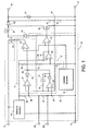
- FIG. 1 schematically illustrates an embodiment of a portion of a power controller 10 that has a pass-through zone that facilitates high efficiency operation.
- Controller 10 includes a buck controller 11 and a boost controller 12 interconnected in tandem to provide an output voltage having a desired value.
- Controller 10 receives an input voltage between a voltage input 13 and a voltage return 14, and responsively generates an output voltage between a voltage output 16 and a voltage return 17. Return 17 typically is connected to return 14.
- Buck controller 11 and boost controller 12 are pointed out in general by dashed boxes.
- a kick-back diode 43 assists in operating buck controller 11
- a boost diode 62 assists in operating boost controller 12, and an inductor 61 is shared by the operation of both controllers 11 and 12.
- Buck controller 11 includes a first error amplifier 31, a buck comparator 41, and a buck output switch or output transistor 42.
- Boost controller 12 includes a second error amplifier 32, an adder-subtracter amplifier 56, a boost comparator 57, and a boost output switch or output transistor 58.
- a resistor 36 and a capacitor 37 form a compensation network that provides phase compensation to stabilize the feedback loop and minimize oscillation in the output voltage at output 16.
- transistor 42 is a P-Channel power MOS transistor and transistor 58 is an N-Channel power MOS transistor but may also be other switch devices capable of supplying the desired current.
- a feedback network includes resistors 22 and 23 connected in series between output 16 and return 17 to form a feedback voltage at a node 24 that is representative of the output voltage on output 16.
- the feedback network typically is external to controller 10, but may be within controller 10 in some embodiments.
- a reference generator 19 of controller 10 provides a reference voltage on an output of generator 19.
- Generator 19 can be one of various implementations that are well-known to those skilled of the art including a bandgap reference generator.
- a signal generator 18 is also included in controller 10.
- Generator 18 generates an oscillating signal that facilitates switching transistors 42 and 58 at a periodic rate. In the preferred embodiment, the oscillating signal from generator 18 has a sawtooth wave shape that varies between two voltages that are greater than the voltage on return 14.
- An output capacitor 21 functions to filter the output voltage from controller 10.
- Other well known functions and circuits such as soft start, under voltage lock-out, over voltage protection, current limit, thermal protection, current mode control, or voltage mode control may also be included as a portion of controller 10.
- Transistors 42 and 58, resistors 22 and 23, diodes 43 and 62, and capacitor 21 typically are external to controller 10 but any or all may be included within controller 10 in some embodiments.
- the input voltage applied between input 13 and return 14 is a voltage that varies both above and below the desired value of the output voltage.
- the pass-through zone formed by controller 10 increases the operational efficiency while forming the output voltage from the varying input voltage.
- the pass-through zone is a range of output voltage values for which controller 10 continuously connects the input voltage to output 16 to generate the output voltage.
- the pass-through zone has a first voltage or upper limit and a second voltage or lower limit.
- controller 10 continuously enables transistor 42 and disables transistor 58 in order to couple the input voltage to output 16 to keep the output voltage within the desired range.
- buck controller 11 and boost controller 12 are inhibited from operating in the switching mode.
- boost controller 12 disables transistor 58 and buck controller 11 operates in the switching mode by driving transistor 42 with the oscillating signal to decrease the value of the output voltage.
- boost controller 11 continuously enables transistor 42 and boost controller 12 operates in the switching mode by driving transistor 58 with the oscillating signal to increase the value of the output voltage. Consequently, when the output voltage is greater than or less than the pass-through zone, controller 10 switchingly couples the input voltage to output 16.
- the output voltage may only be a few microvolts greater than or less than the respective upper or lower limits of the pass-through zone.
- the upper and lower limits are no greater than about ten percent (10%) above and below the desired value of the output voltage however the amount depends on the amount of regulation desired in the output voltage.
- a reference divider network comprising resistors 26, 27, and 29 along with associated reference nodes 46 and 47 are connected in series between the output of generator 19 and return 14.
- the reference divider network provides two different reference voltage values that are used by amplifiers 31 and 32 to establish the upper and lower limits of the pass-through zone.
- the reference voltage at node 46 establishes the output voltage value representing the upper limit of the pass-through zone
- the reference voltage at node 47 establishes the output voltage value representing the lower limit of the pass-through zone.
- resistor 27 may be omitted and an external resistor may be connected to optional inputs 44 and 45 to function for resistor 27. Such an external resistor provides a method to adjust the reference voltage values.
- resistor 27 can remain and an external resistor connected to inputs 44 and 45 in parallel with resistor 27.
- the output of amplifiers 31 and 32 are logically "OR" ed together, through diodes 33 and 34, to form a single control voltage at a control node 38.
- the control voltage is used to control the operation of both controllers 11 and 12 and transistors 42 and 58.
- the output of amplifier 31 is driven to a high level that reverse biases diode 33 and prevents amplifier 31 from driving node 38.
- the output of amplifier 32 is driven to a low level that reverse biases diode 34 and prevents amplifier 32 from driving node 38.
- Resistors 49, 51, and 52 form a resistor divider that sets the level of the control voltage that is applied to amplifier 56.
- resistors 49, 51, and 52 are selected so that when neither amplifier 31 nor 32 is driving node 38, resistors 49, 51, and 52 provide a voltage at node 38 that is larger than the maximum value of the oscillating signal applied to comparator 41. This ensures that comparator 41 enables transistor 42 to couple the input voltage to output 16 and that comparator 57 disables transistor 58.
- resistors 49, 51, 52, 53, and 54 are selected to provide a voltage at the output of amplifier 56 that is approximately equal to the control voltage at node 38 minus an offset that is larger than the peak-to-peak amplitude of oscillating signal. This condition ensures that the output of comparator 57 is low and transistor 58 is disabled.
- the output of amplifier 31 is a high voltage and the output of amplifier 32 is a low voltage and diodes 33 and 34 block amplifiers 31 and 32 from driving node 38. Since resistors 49, 51, and 52 form a voltage at node 38 that is larger than the maximum value of the oscillating signal, the output of comparator 41 is low and transistor 42 is enabled to connect the input voltage to output 16. Also, the output of amplifier 56 provides a voltage that drives the output of comparator 57 low to disable transistor 58.
- comparator 41 responsively generates pulses that switchingly drive transistor 42. The pulses occur whenever the control voltage at node 38 is less than the upper value of the oscillating signal from generator 18. The pulses from the output of comparator 41 switch transistor 42 thereby operating controller 10 in the buck mode and reducing the value of the output voltage. Controller 10 continues to operate in the buck mode as long as the value of the output voltage is greater than the upper limit of the pass-through zone.
- the feedback voltage decreases to a value that is less than the reference voltage at node 47. Consequently, the output voltage of amplifier 32 increases and correspondingly increases the control voltage.
- the high control voltage causes the output of amplifier 56 to increase past the lower limit of the oscillating signal thereby enabling comparator 57 to generate pulses to switchingly drive transistor 58 and operate controller 10 in the boost mode.
- the pulses occur whenever the output of amplifier 56 is greater than the lower value of the oscillating signal from generator 18.
- the feedback voltage also increases causing a corresponding decrease in the output of amplifier 32 until the output voltage is no less than the lower limit of the pass-through zone.
- the output of amplifier 56 responsively decreases past the lower limit of the oscillating signal thereby forcing the output of comparator 57 low and disabling transistor 58.
- the desired output voltage was twenty-four volts (24 V) and the upper and lower limits of the pass-through zone were twenty-six volts (26 V) and twenty-two volts (22 V), respectively.
- Resistors 26, 27, and 29 were selected to provide reference voltages of 2.6 volts at node 46 and 2.2 volts at node 47.
- Resistors 22 and 23 were selected to provide a feedback voltage of 2.4 volts when the output voltage was twenty-four volts (24 V).
- the values of resistors 49, 51, 52, 53, and 54 were chosen so that adder-subtractor amplifier 56 subtracted 2.5 volts from the control voltage at node 38.
- the oscillating signal had upper and lower peak values of two volts (2.0 V) and one volt (1.0 V), respectively. Consequently the value of the control voltage would be 2.5 volts when amplifiers 31 and 32 were not driving node 38.
- the input voltage applied between input 13 and return 14 was a half wave rectified and filtered voltage that varied between about eighteen volts (18 V) and thirty volts (30 V). In this example embodiment, controller 10 operated with an efficiency that was approximately ten percent (10%) greater than prior art controllers.
- a first terminal of resistor 26 is connected to the output of generator 19 and a second terminal is connected to both node 46 and to a first terminal of resistor 27.
- a second terminal of resistor 27 is connected to node 47 and to a first terminal of resistor 29.
- a second terminal of resistor 29 is connected to return 14.
- Resistor 22 has a first terminal connected to output 16 and a second terminal connected to both node 24 and to a first terminal of resistor 23 which has a second terminal connected to return 14.
- Amplifier 31 has a positive input connected to node 46, an inverting input connected to node 24, and an output connected to a cathode of diode 33.
- An anode of diode 33 is connected to node 38 and to a cathode of diode 34.
- An anode of diode 34 is connected to the output of amplifier 32.
- a positive input of amplifier 32 is connected to node 47 and an inverting input is connected to both node 24 and a first terminal of resistor 36.
- a second terminal of resistor 36 is connected to a first terminal of capacitor 37 which has a second terminal connected to the cathode of diode 34.
- Resistor 49 has a first terminal connected to the output of generator 19 and a second terminal connected to node 38 and to a first terminal of resistor 51.
- a second terminal of resistor 51 is connected to the positive input of amplifier 56 and to a first terminal of resistor 52 which has a second terminal connected to return 14.
- An inverting input of amplifier 56 is connected to a first terminal of resistor 54 and to a first terminal of resistor 53, and an output of amplifier 56 is connected to a second terminal of resistor 54.
- a second terminal of resistor 53 is connected to the output of generator 19.
- Generator 18 has an output connected to a negative input of comparator 57 and a positive input of comparator 41.
- Comparator 41 has a negative input connected to node 38 and an output connected to the gate of transistor 42.
- a source of transistor 42 is connected to input 13 and a drain is connected to both a cathode of diode 43 and a first terminal of inductor 61.
- An anode of diode 43 is connected to return 14.
- a second terminal of inductor 61 is connected to the anode of diode 62 and to the drain of transistor 58.
- a source of transistor 58 is connected to return 14 and a gate of transistor 58 is connected to the output of comparator 57.
- a positive input of comparator 57 is connected to the output of amplifier 56.
- a first terminal of capacitor 21 is connected to output 16 and to the cathode of diode 62, and a second terminal of capacitor 21 is connected to return 14.
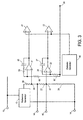
- FIG. 2 schematically illustrates a portion of an embodiment of a power controller 70 that is an alternate embodiment of power controller 10 explained in the description of FIG. 1.
- Controller 70 couples a boost converter 72 before a buck converter 71.
- Boost converter 72 is followed in the tandem configuration with buck converter 71. This is the opposite arrangement to that of controller 10.
- Inductor 61 and diode 43 are positioned between transistor 42 and output 16.
- An additional input inductor 64 is coupled in series with diode 62.
- a filter capacitor 65 is connected to receive the output voltage of boost converter 72 and store the energy for use by converter 71.
- converter 70 has minimal high-frequency ripple current at input 13, and converter 70 also provides capacitor 21 with a continuous output current resulting in less high-frequency ripple voltage at output 16.
- Transistors 42 and 58, diodes 43 and 62, resistors 22 and 23, inductors 61 and 64, and capacitors 21 and 65 typically are external to controller 70 but any or all may be included within controller 10 in other embodiments.
- controller 70 elements of controller 70 that control comparators 41 and 57 are connected in the same manner as the same elements of controller 10.
- transistors 42 and 58 are connected differently.
- the source of transistor 58 connected to return 14, the gate is connected to the output of comparator 57, and the drain is connected to a first terminal of inductor 64 and to an anode of diode 62.
- a second terminal of inductor 64 is connected to input 13.
- a cathode of diode 62 is connected to a first terminal of capacitor 65 and to a source of transistor 42.
- a drain of transistor 42 is connected to a cathode of diode 43 and to a first terminal of inductor 61, and the gate is connected to the output of comparator 41.
- a second terminal of inductor 61 is connected output 16.
- the anode of diode 43 and a second terminal of capacitor 65 are connected to return 14.
- FIG. 3 schematically illustrates an alternate embodiment of a portion of power controller 10 explained in the description of FIG. 1.
- the outputs of amplifiers 31 and 32 are separated to form two control voltages instead of the single control voltage generated in the embodiment of FIG. 1.
- the output of amplifier 31 forms a first control voltage that drives comparator 41 directly to switchingly drive transistor 42 when the output voltage is greater than the upper limit of the pass-through zone.
- the output of amplifier 32 forms a second control voltage that drives comparator 57 directly to switchingly drive transistor 58 when the output voltage is less than the lower limit of the pass-through zone. Consequently, diodes 33 and 34, resistors 49, 51, 52, 53, and 54, and amplifier 56 are omitted.
- a compensation network of a resistor 39 and a capacitor 40 may be coupled to amplifier 31 to improve the stability of controller 10 in a manner similar to resistor 36 and capacitor 37. Using separate compensation for the upper and lower limits of the pass-through zone improves the stability of the controller. Additionally, input resistors 66 and 67 couple the feedback voltage to the inputs of amplifiers 31 and 32. Resistors 66 and 67 assist in providing some isolation between the inputs to amplifiers 31 and 32.
- the output of amplifier 31 is connected to the inverting input of comparator 41 and to a first terminal of capacitor 40.
- a second terminal of capacitor 40 is connected to a first terminal of resistor 39 which has a second terminal connected to the inverting input of amplifier 31.
- the output of amplifier 32 is connected to the positive input of comparator 57.
- FIG. 4 illustrates an enlarged plan view of a semiconductor device 80 that includes high efficiency power controller 10 explained in the description of FIG. 1.
- Device 80 is formed on a semiconductor die 81.
- Forming the pass-through voltage zone facilitates coupling the input voltage to the output to form the output voltage in a controlled manner to increase the efficiency of the voltage conversion.
- Using an upper voltage limit and a lower voltage limit provides voltage levels to transition between continuously coupling the input voltage to the output and switching the output transistors to form the output voltage.
Landscapes
- Engineering & Computer Science (AREA)
- Power Engineering (AREA)
- Dc-Dc Converters (AREA)
Abstract
Description
- The present invention relates, in general, to electronics, and more particularly, to methods of forming power conversion devices.
- In the past, various methods and circuits were utilized to implement power conversion functions. One typical configuration, referred to as a buck converter, was used to regulate an output voltage that had a value that was less than an input voltage. The buck converter typically included a switching transistor that was controlled by a pulse width modulation controller or other similar controller. The switching transistor was enabled in a switching mode to supply power from the input voltage to the output as the output voltage decreased below a desired value. Another typical configuration, referred to as a boost converter, was used to regulate an output voltage that had a value that was greater than the input voltage. The boost converter also utilized a switching transistor that was operated in a switching mode to boost the value of the input voltage to the desired output voltage value. In some applications, a boost converter and a buck converter were connected together in series or in tandem to provide a more regulated output voltage than either the boost converter or buck converter could individually provide. The tandem coupled buck and boost converters operated the switching transistors similarly to the separate boost or buck converter. One problem with this tandem configuration was efficiency. With both converters processing power in the switching mode, the overall efficiency was the product of the two efficiencies, thus, the efficiency was lower than desired. The lower efficiency resulted in excess power dissipation and heat as well as increased operating costs.
- Accordingly, it is desirable to have a power conversion method that has increased efficiency.
-
- FIG. 1 schematically illustrates a portion of an embodiment of a high efficiency power controller in accordance with the present invention;
- FIG. 2 schematically illustrates a portion of another embodiment of a high efficiency power controller in accordance with the present invention;
- FIG. 3 schematically illustrates an alternate embodiment of a portion of the power controllers of FIG. 1 and FIG. 2 in accordance with the present invention; and
- FIG. 4 illustrates an enlarged plan view of a semiconductor device that includes a high efficiency power controller in accordance with the present invention.
-
- For simplicity and clarity of illustration, elements in the figures are not necessarily to scale, and the same reference numbers in different figures denote the same elements. Additionally, descriptions and details of well known steps and elements are omitted for simplicity of the description. As used herein current carrying electrode means an element of a device that carries current through the device such as a source or a drain of an MOS transistor or an emitter or a collector of a bipolar transistor, and a control electrode means an element of the device that controls current through the device such as a gate of an MOS transistor or a base of a bipolar transistor.
- FIG. 1 schematically illustrates an embodiment of a portion of a
power controller 10 that has a pass-through zone that facilitates high efficiency operation.Controller 10 includes abuck controller 11 and aboost controller 12 interconnected in tandem to provide an output voltage having a desired value.Controller 10 receives an input voltage between avoltage input 13 and avoltage return 14, and responsively generates an output voltage between avoltage output 16 and avoltage return 17.Return 17 typically is connected to return 14.Buck controller 11 andboost controller 12 are pointed out in general by dashed boxes. A kick-back diode 43 assists inoperating buck controller 11, aboost diode 62 assists inoperating boost controller 12, and aninductor 61 is shared by the operation of bothcontrollers -
Buck controller 11 includes afirst error amplifier 31, abuck comparator 41, and a buck output switch oroutput transistor 42.Boost controller 12 includes asecond error amplifier 32, an adder-subtracter amplifier 56, aboost comparator 57, and a boost output switch oroutput transistor 58. Aresistor 36 and acapacitor 37 form a compensation network that provides phase compensation to stabilize the feedback loop and minimize oscillation in the output voltage atoutput 16. Typicallytransistor 42 is a P-Channel power MOS transistor andtransistor 58 is an N-Channel power MOS transistor but may also be other switch devices capable of supplying the desired current. - A feedback network includes
resistors output 16 and return 17 to form a feedback voltage at anode 24 that is representative of the output voltage onoutput 16. The feedback network typically is external to controller 10, but may be withincontroller 10 in some embodiments. Areference generator 19 ofcontroller 10 provides a reference voltage on an output ofgenerator 19.Generator 19 can be one of various implementations that are well-known to those skilled of the art including a bandgap reference generator. Asignal generator 18 is also included incontroller 10.Generator 18 generates an oscillating signal that facilitatesswitching transistors generator 18 has a sawtooth wave shape that varies between two voltages that are greater than the voltage onreturn 14. Such oscillating signals are well known to those skilled in the art. Anoutput capacitor 21 functions to filter the output voltage fromcontroller 10. Other well known functions and circuits such as soft start, under voltage lock-out, over voltage protection, current limit, thermal protection, current mode control, or voltage mode control may also be included as a portion ofcontroller 10.Transistors resistors diodes capacitor 21 typically are external to controller 10 but any or all may be included withincontroller 10 in some embodiments. - Typically, the input voltage applied between
input 13 andreturn 14 is a voltage that varies both above and below the desired value of the output voltage. The pass-through zone formed bycontroller 10 increases the operational efficiency while forming the output voltage from the varying input voltage. The pass-through zone is a range of output voltage values for whichcontroller 10 continuously connects the input voltage tooutput 16 to generate the output voltage. In general, the pass-through zone has a first voltage or upper limit and a second voltage or lower limit. When the output voltage is no greater than the upper limit and no less than the lower limit,controller 10 continuously enablestransistor 42 and disablestransistor 58 in order to couple the input voltage to output 16 to keep the output voltage within the desired range. Thus,buck controller 11 andboost controller 12 are inhibited from operating in the switching mode. When the value of the output voltage is greater than the upper limit of the pass-through zone,boost controller 12 disablestransistor 58 andbuck controller 11 operates in the switching mode bydriving transistor 42 with the oscillating signal to decrease the value of the output voltage. When the value of the output voltage is less than the lower limit of the pass-through zone,buck controller 11 continuously enablestransistor 42 andboost controller 12 operates in the switching mode by drivingtransistor 58 with the oscillating signal to increase the value of the output voltage. Consequently, when the output voltage is greater than or less than the pass-through zone,controller 10 switchingly couples the input voltage to output 16. Those skilled in the art will realize that because of the high gain of the feedback circuit, the output voltage may only be a few microvolts greater than or less than the respective upper or lower limits of the pass-through zone. Typically the upper and lower limits are no greater than about ten percent (10%) above and below the desired value of the output voltage however the amount depends on the amount of regulation desired in the output voltage. - A reference divider
network comprising resistors reference nodes generator 19 andreturn 14. The reference divider network provides two different reference voltage values that are used byamplifiers node 46 establishes the output voltage value representing the upper limit of the pass-through zone, and the reference voltage atnode 47 establishes the output voltage value representing the lower limit of the pass-through zone. In some embodiments,resistor 27 may be omitted and an external resistor may be connected tooptional inputs resistor 27. Such an external resistor provides a method to adjust the reference voltage values. In other embodiments,resistor 27 can remain and an external resistor connected toinputs resistor 27. - The output of
amplifiers diodes control node 38. The control voltage is used to control the operation of bothcontrollers transistors node 46, the output ofamplifier 31 is driven to a high level thatreverse biases diode 33 and preventsamplifier 31 fromdriving node 38. Similarly, when the value of the feedback voltage is greater than the voltage atnode 47, the output ofamplifier 32 is driven to a low level thatreverse biases diode 34 and preventsamplifier 32 fromdriving node 38. Thus, whenamplifier 31 is high andamplifier 32 islow node 38 is not driven.Resistors amplifier 56. Typically resistors 49, 51, and 52 are selected so that when neitheramplifier 31 nor 32 is drivingnode 38,resistors node 38 that is larger than the maximum value of the oscillating signal applied tocomparator 41. This ensures thatcomparator 41 enablestransistor 42 to couple the input voltage tooutput 16 and thatcomparator 57 disablestransistor 58. Also under this condition of neitheramplifier 31 nor 32 drivingnode 38,resistors amplifier 56 that is approximately equal to the control voltage atnode 38 minus an offset that is larger than the peak-to-peak amplitude of oscillating signal. This condition ensures that the output ofcomparator 57 is low andtransistor 58 is disabled. - In operation, when the output voltage on
output 16 is within the past-through zone, the feedback voltage atnode 24 is less than the reference voltage atnode 46 and greater than the reference voltage atnode 47. Thus, the output ofamplifier 31 is a high voltage and the output ofamplifier 32 is a low voltage anddiodes block amplifiers node 38. Sinceresistors node 38 that is larger than the maximum value of the oscillating signal, the output ofcomparator 41 is low andtransistor 42 is enabled to connect the input voltage tooutput 16. Also, the output ofamplifier 56 provides a voltage that drives the output ofcomparator 57 low to disabletransistor 58. - If the value of the output voltage increases sufficiently to cause the value of the feedback voltage at
node 24 to exceed the value of the reference voltage atnode 46, the output ofamplifier 31 will decrease causing a decrease in the control voltage atnode 38. When the value of the control voltage decreases past the upper value of the oscillating signal,comparator 41 responsively generates pulses that switchinglydrive transistor 42. The pulses occur whenever the control voltage atnode 38 is less than the upper value of the oscillating signal fromgenerator 18. The pulses from the output ofcomparator 41switch transistor 42 thereby operatingcontroller 10 in the buck mode and reducing the value of the output voltage.Controller 10 continues to operate in the buck mode as long as the value of the output voltage is greater than the upper limit of the pass-through zone. - If the output voltage decreases to a value that is less than the lower limit of the pass-through zone, the feedback voltage decreases to a value that is less than the reference voltage at
node 47. Consequently, the output voltage ofamplifier 32 increases and correspondingly increases the control voltage. The high control voltage causes the output ofamplifier 56 to increase past the lower limit of the oscillating signal thereby enablingcomparator 57 to generate pulses to switchinglydrive transistor 58 and operatecontroller 10 in the boost mode. The pulses occur whenever the output ofamplifier 56 is greater than the lower value of the oscillating signal fromgenerator 18. As the value of the output voltage increases from the boost mode operation, the feedback voltage also increases causing a corresponding decrease in the output ofamplifier 32 until the output voltage is no less than the lower limit of the pass-through zone. The output ofamplifier 56 responsively decreases past the lower limit of the oscillating signal thereby forcing the output ofcomparator 57 low and disablingtransistor 58. - In one example embodiment of
controller 10, the desired output voltage was twenty-four volts (24 V) and the upper and lower limits of the pass-through zone were twenty-six volts (26 V) and twenty-two volts (22 V), respectively.Resistors node 46 and 2.2 volts atnode 47.Resistors resistors subtractor amplifier 56 subtracted 2.5 volts from the control voltage atnode 38. The oscillating signal had upper and lower peak values of two volts (2.0 V) and one volt (1.0 V), respectively. Consequently the value of the control voltage would be 2.5 volts whenamplifiers node 38. The input voltage applied betweeninput 13 and return 14 was a half wave rectified and filtered voltage that varied between about eighteen volts (18 V) and thirty volts (30 V). In this example embodiment,controller 10 operated with an efficiency that was approximately ten percent (10%) greater than prior art controllers. - In order to facilitate this functionality, a first terminal of
resistor 26 is connected to the output ofgenerator 19 and a second terminal is connected to bothnode 46 and to a first terminal ofresistor 27. A second terminal ofresistor 27 is connected tonode 47 and to a first terminal ofresistor 29. A second terminal ofresistor 29 is connected to return 14.Resistor 22 has a first terminal connected tooutput 16 and a second terminal connected to bothnode 24 and to a first terminal ofresistor 23 which has a second terminal connected to return 14.Amplifier 31 has a positive input connected tonode 46, an inverting input connected tonode 24, and an output connected to a cathode ofdiode 33. An anode ofdiode 33 is connected tonode 38 and to a cathode ofdiode 34. An anode ofdiode 34 is connected to the output ofamplifier 32. A positive input ofamplifier 32 is connected tonode 47 and an inverting input is connected to bothnode 24 and a first terminal ofresistor 36. A second terminal ofresistor 36 is connected to a first terminal ofcapacitor 37 which has a second terminal connected to the cathode ofdiode 34.Resistor 49 has a first terminal connected to the output ofgenerator 19 and a second terminal connected tonode 38 and to a first terminal ofresistor 51. A second terminal ofresistor 51 is connected to the positive input ofamplifier 56 and to a first terminal ofresistor 52 which has a second terminal connected to return 14. An inverting input ofamplifier 56 is connected to a first terminal ofresistor 54 and to a first terminal ofresistor 53, and an output ofamplifier 56 is connected to a second terminal ofresistor 54. A second terminal ofresistor 53 is connected to the output ofgenerator 19.Generator 18 has an output connected to a negative input ofcomparator 57 and a positive input ofcomparator 41.Comparator 41 has a negative input connected tonode 38 and an output connected to the gate oftransistor 42. A source oftransistor 42 is connected to input 13 and a drain is connected to both a cathode ofdiode 43 and a first terminal ofinductor 61. An anode ofdiode 43 is connected to return 14. A second terminal ofinductor 61 is connected to the anode ofdiode 62 and to the drain oftransistor 58. A source oftransistor 58 is connected to return 14 and a gate oftransistor 58 is connected to the output ofcomparator 57. A positive input ofcomparator 57 is connected to the output ofamplifier 56. A first terminal ofcapacitor 21 is connected tooutput 16 and to the cathode ofdiode 62, and a second terminal ofcapacitor 21 is connected to return 14. - FIG. 2 schematically illustrates a portion of an embodiment of a
power controller 70 that is an alternate embodiment ofpower controller 10 explained in the description of FIG. 1.Controller 70 couples aboost converter 72 before abuck converter 71.Boost converter 72 is followed in the tandem configuration withbuck converter 71. This is the opposite arrangement to that ofcontroller 10. Because of the different connections, the configuration ofdiodes inductor 61 are also different than those ofcontroller 10.Inductor 61 anddiode 43 are positioned betweentransistor 42 andoutput 16. Anadditional input inductor 64 is coupled in series withdiode 62. Afilter capacitor 65 is connected to receive the output voltage ofboost converter 72 and store the energy for use byconverter 71. In addition to high efficiency,converter 70 has minimal high-frequency ripple current atinput 13, andconverter 70 also providescapacitor 21 with a continuous output current resulting in less high-frequency ripple voltage atoutput 16.Transistors diodes resistors inductors capacitors controller 70 but any or all may be included withincontroller 10 in other embodiments. - In order to facilitate this functionality, elements of
controller 70 that controlcomparators controller 10. However,transistors transistor 58 connected to return 14, the gate is connected to the output ofcomparator 57, and the drain is connected to a first terminal ofinductor 64 and to an anode ofdiode 62. A second terminal ofinductor 64 is connected to input 13. A cathode ofdiode 62 is connected to a first terminal ofcapacitor 65 and to a source oftransistor 42. A drain oftransistor 42 is connected to a cathode ofdiode 43 and to a first terminal ofinductor 61, and the gate is connected to the output ofcomparator 41. A second terminal ofinductor 61 is connectedoutput 16. The anode ofdiode 43 and a second terminal ofcapacitor 65 are connected to return 14. - FIG. 3 schematically illustrates an alternate embodiment of a portion of
power controller 10 explained in the description of FIG. 1. In the alternate embodiment of FIG. 3, the outputs ofamplifiers amplifier 31 forms a first control voltage that drivescomparator 41 directly toswitchingly drive transistor 42 when the output voltage is greater than the upper limit of the pass-through zone. Similarly, the output ofamplifier 32 forms a second control voltage that drivescomparator 57 directly toswitchingly drive transistor 58 when the output voltage is less than the lower limit of the pass-through zone. Consequently,diodes resistors amplifier 56 are omitted. A compensation network of aresistor 39 and acapacitor 40 may be coupled toamplifier 31 to improve the stability ofcontroller 10 in a manner similar toresistor 36 andcapacitor 37. Using separate compensation for the upper and lower limits of the pass-through zone improves the stability of the controller. Additionally,input resistors amplifiers Resistors amplifiers - To facilitate this operation, the output of
amplifier 31 is connected to the inverting input ofcomparator 41 and to a first terminal ofcapacitor 40. A second terminal ofcapacitor 40 is connected to a first terminal ofresistor 39 which has a second terminal connected to the inverting input ofamplifier 31. The output ofamplifier 32 is connected to the positive input ofcomparator 57. - FIG. 4 illustrates an enlarged plan view of a
semiconductor device 80 that includes highefficiency power controller 10 explained in the description of FIG. 1.Device 80 is formed on asemiconductor die 81. - In view of all of the above, it is evident that a novel device and method is disclosed. Forming the pass-through voltage zone facilitates coupling the input voltage to the output to form the output voltage in a controlled manner to increase the efficiency of the voltage conversion. Using an upper voltage limit and a lower voltage limit provides voltage levels to transition between continuously coupling the input voltage to the output and switching the output transistors to form the output voltage.
Claims (9)
- A method of forming a high efficiency power controller comprising:providing a boost converter (12) coupled in tandem with a buck converter (11) to receive an input voltage (13) and generate an output voltage on an output (16) of the high efficiency power controller;forming the high efficiency power controller to operate the buck converter in a switching mode when the output voltage is greater than a first value and to operate the boost converter in a switching mode when the output voltage is less than a second value wherein the first value is greater than the second value; andforming the high efficiency power controller to constantly couple the input voltage to the output and not operate the buck converter or the boost converter in a switching mode when the output voltage is less than the first value and greater than the second value.
- The method of claim 1 wherein forming the high efficiency power controller to constantly couple the input voltage to the output includes forming the high efficiency power controller to constantly enable an output transistor (42) of the buck converter and disable an output transistor (58) of the boost converter.
- The method of claim 2 wherein forming the high efficiency power controller to constantly enable the output transistor of the buck converter and disable the output transistor of the boost converter includes coupling a first amplifier (31) to receive a feedback voltage (24) representative of the output voltage and to receive a first reference voltage (46) and responsively generate a control voltage (38) and including using the control voltage to enable the output transistor (42) of the buck converter, and coupling a second amplifier (56) to receive the control voltage and using an output of the second amplifier to disable the output transistor (58) of the boost converter.
- The method of claim 1 wherein forming the high efficiency power controller to constantly couple the input voltage to the output and not operate the buck converter or the boost converter in a switching mode when the output voltage is less than the first value and greater than the second value includes forming the high efficiency power controller to generate a control voltage (38) having a first voltage representative of the first value and a second voltage representative of the second value.
- The method of claim 4 wherein forming the high efficiency power controller to generate the control voltage having the first voltage representative of the first value and the second voltage representative of the second value includes coupling a first amplifier (31) to receive a feedback voltage representative of the output voltage and to receive a first reference voltage, and coupling a second amplifier (56) to receive a second reference voltage (47) and the control voltage (38).
- The method of claim 5 further including coupling a first comparator (57) to receive an output of the second amplifier (56) and receive an oscillating signal (20) and responsively drive an output transistor (58) of the boost converter.
- The method of claim 6 further including coupling a second comparator (41) to receive the control voltage (38) and receive the oscillating signal (20) and responsively drive an output transistor (42) of the buck converter.
- The method of claim 7 further including coupling a third amplifier (32) to receive the feedback voltage and to receive a third reference voltage (47), and coupling an output of the third amplifier to an output of the first amplifier (31).
- The method of claim 4 further including coupling a first comparator (41) to receive the control voltage (38) and receive an oscillating voltage (20) and responsively drive an output transistor (42) of the buck converter.
Applications Claiming Priority (2)
| Application Number | Priority Date | Filing Date | Title |
|---|---|---|---|
| US10/638,227 US6936997B2 (en) | 2003-08-11 | 2003-08-11 | Method of forming a high efficiency power controller |
| US638227 | 2003-08-11 |
Publications (3)
| Publication Number | Publication Date |
|---|---|
| EP1508960A2 true EP1508960A2 (en) | 2005-02-23 |
| EP1508960A3 EP1508960A3 (en) | 2006-05-31 |
| EP1508960B1 EP1508960B1 (en) | 2020-01-22 |
Family
ID=34063433
Family Applications (1)
| Application Number | Title | Priority Date | Filing Date |
|---|---|---|---|
| EP04076985.3A Expired - Fee Related EP1508960B1 (en) | 2003-08-11 | 2004-07-09 | Method of forming a high efficiency power controller |
Country Status (4)
| Country | Link |
|---|---|
| US (1) | US6936997B2 (en) |
| EP (1) | EP1508960B1 (en) |
| CN (1) | CN100489723C (en) |
| HK (1) | HK1073894A1 (en) |
Cited By (1)
| Publication number | Priority date | Publication date | Assignee | Title |
|---|---|---|---|---|
| US10686381B1 (en) | 2019-02-27 | 2020-06-16 | Analog Devices International Unlimited Company | Synchronous boost regulator circuit with pass-through operation control |
Families Citing this family (32)
| Publication number | Priority date | Publication date | Assignee | Title |
|---|---|---|---|---|
| JP2005086843A (en) * | 2003-09-04 | 2005-03-31 | Taiyo Yuden Co Ltd | Output control device of power supply source |
| JP4426807B2 (en) * | 2003-10-02 | 2010-03-03 | セイコーインスツル株式会社 | Buck-boost switching regulator control circuit and buck-boost switching regulator |
| JP2005117784A (en) * | 2003-10-08 | 2005-04-28 | Rohm Co Ltd | Switching power supply apparatus |
| JP3600915B1 (en) * | 2003-10-09 | 2004-12-15 | ローム株式会社 | Switching power supply device and electronic device with display device |
| KR100577325B1 (en) * | 2003-11-14 | 2006-05-10 | 마쯔시다덴기산교 가부시키가이샤 | Dc-dc converter |
| TWI242928B (en) * | 2004-09-10 | 2005-11-01 | Richtek Techohnology Corp | Electronic circuit using normally-on junction field effect transistor |
| EP1792398B1 (en) * | 2004-09-14 | 2016-08-03 | Nxp B.V. | Dc/dc converter with dynamic offset compensation |
| US6987378B1 (en) * | 2004-12-02 | 2006-01-17 | Semiconductor Components Industries, L.L.C. | Over-voltage protection circuit and method therefor |
| US20060132105A1 (en) * | 2004-12-16 | 2006-06-22 | Prasad Atluri R | Controlling inrush current |
| US7679874B2 (en) * | 2005-07-25 | 2010-03-16 | Semiconductor Components Industries, L.L.C. | Power overload detection method and structure therefor |
| US7218080B2 (en) * | 2005-09-13 | 2007-05-15 | System-General Corporation | Soft-start apparatus for power supplies |
| KR100866967B1 (en) * | 2007-05-10 | 2008-11-05 | 삼성전자주식회사 | Irregular voltage detection and cutoff circuit using bandgap reference voltage generation circuit |
| US20090256534A1 (en) * | 2008-04-14 | 2009-10-15 | Twisthink, L.L.C. | Power supply control method and apparatus |
| US8541991B2 (en) | 2008-04-16 | 2013-09-24 | Enpirion, Inc. | Power converter with controller operable in selected modes of operation |
| US8692532B2 (en) | 2008-04-16 | 2014-04-08 | Enpirion, Inc. | Power converter with controller operable in selected modes of operation |
| US8686698B2 (en) | 2008-04-16 | 2014-04-01 | Enpirion, Inc. | Power converter with controller operable in selected modes of operation |
| US9246390B2 (en) | 2008-04-16 | 2016-01-26 | Enpirion, Inc. | Power converter with controller operable in selected modes of operation |
| US9548714B2 (en) | 2008-12-29 | 2017-01-17 | Altera Corporation | Power converter with a dynamically configurable controller and output filter |
| US8698463B2 (en) * | 2008-12-29 | 2014-04-15 | Enpirion, Inc. | Power converter with a dynamically configurable controller based on a power conversion mode |
| US8867295B2 (en) | 2010-12-17 | 2014-10-21 | Enpirion, Inc. | Power converter for a memory module |
| CN103176025B (en) * | 2011-12-22 | 2015-02-04 | 上海华虹宏力半导体制造有限公司 | Power source voltage detection circuit and control method thereof |
| JP6007804B2 (en) * | 2013-01-28 | 2016-10-12 | 株式会社ソシオネクスト | Power supply control circuit, power supply device, electronic device, and power supply control method |
| JP2014222969A (en) * | 2013-05-13 | 2014-11-27 | 株式会社オートネットワーク技術研究所 | Voltage conversion device |
| US9256236B2 (en) * | 2013-07-26 | 2016-02-09 | Analog Devices, Inc. | Area-efficient frequency compensation |
| CN103887983A (en) * | 2014-03-21 | 2014-06-25 | 浙江大学 | Control method for double-tube cascade type buck-boost converter |
| US9509217B2 (en) | 2015-04-20 | 2016-11-29 | Altera Corporation | Asymmetric power flow controller for a power converter and method of operating the same |
| US10069439B2 (en) * | 2015-12-22 | 2018-09-04 | Renesas Electronics Corporation | Power conversion system, power module, and semiconductor device with diode coupling |
| US10116216B2 (en) | 2016-03-29 | 2018-10-30 | Semiconductor Components Industries, Llc | Ultrasonic control system and method for a buck-boost power converter |
| JP6954205B2 (en) * | 2018-03-28 | 2021-10-27 | トヨタ自動車株式会社 | Power converter |
| JP7140699B2 (en) * | 2019-03-15 | 2022-09-21 | 株式会社東芝 | Power supply circuit and control method for power supply circuit |
| US11942865B2 (en) * | 2021-04-29 | 2024-03-26 | Tdk-Lambda Americas Inc. | Non-isolated power module with user adjustable pass-through mode |
| JP2023010088A (en) * | 2021-07-09 | 2023-01-20 | 富士通株式会社 | Power supply device and information processing device |
Citations (4)
| Publication number | Priority date | Publication date | Assignee | Title |
|---|---|---|---|---|
| US5402060A (en) * | 1993-05-13 | 1995-03-28 | Toko America, Inc. | Controller for two-switch buck-boost converter |
| US6037755A (en) * | 1998-07-07 | 2000-03-14 | Lucent Technologies Inc. | Switching controller for a buck+boost converter and method of operation thereof |
| US6191567B1 (en) * | 1999-05-04 | 2001-02-20 | U.S. Philips Corporation | DC-DC converter, with duty cycle comparison for a dual mode back boost converter |
| US20030052654A1 (en) * | 2001-08-07 | 2003-03-20 | Yoshihide Kanakubo | Boosting and step-down switching regulator controlling circuit and boosting and step-down switching regulator for use in the same |
Family Cites Families (15)
| Publication number | Priority date | Publication date | Assignee | Title |
|---|---|---|---|---|
| US519600A (en) * | 1894-05-08 | Car-coupling | ||
| US134355A (en) * | 1872-12-31 | Improvement in drills for drilling metals | ||
| US406470A (en) * | 1889-07-09 | Windmill-tower | ||
| US2241A (en) * | 1841-09-04 | Manufacture of leather hats | ||
| US814696A (en) * | 1904-07-07 | 1906-03-13 | Cooper Hewitt Electric Co | Method of producing light. |
| US838181A (en) * | 1906-04-16 | 1906-12-11 | Walter D Grippin | Window-shade bracket. |
| DE3527801A1 (en) | 1985-08-02 | 1987-02-12 | Frako Kondensator Apparate | METHOD AND CIRCUIT FOR MEASURING THE ACTIVE CURRENT AND THE BLIND CURRENT IN AN ELECTRIC AC SYSTEM |
| US5134355A (en) | 1990-12-31 | 1992-07-28 | Texas Instruments Incorporated | Power factor correction control for switch-mode power converters |
| US5359280A (en) * | 1992-01-10 | 1994-10-25 | Space Systems/Loral | Bilateral power converter for a satellite power system |
| EP0562662B1 (en) | 1992-03-27 | 1997-05-21 | Ascom FRAKO GmbH | AC/DC converter |
| US5568041A (en) | 1995-02-09 | 1996-10-22 | Magnetek, Inc. | Low-cost power factor correction circuit and method for electronic ballasts |
| US5519600A (en) | 1995-03-31 | 1996-05-21 | International Business Machines Corporation | Three-phase self-balancing power supply |
| WO1998009368A1 (en) | 1996-08-30 | 1998-03-05 | Sgs-Thomson Microelectronics | Method and apparatus for automatic average current mode controlled power factor correction without input voltage sensing |
| US6002241A (en) | 1998-10-30 | 1999-12-14 | Lucent Technologies Inc. | Dual mode split-boost converter and method of operation thereof |
| US6788033B2 (en) * | 2002-08-08 | 2004-09-07 | Vlt, Inc. | Buck-boost DC-DC switching power conversion |
-
2003
- 2003-08-11 US US10/638,227 patent/US6936997B2/en not_active Expired - Lifetime
-
2004
- 2004-07-09 EP EP04076985.3A patent/EP1508960B1/en not_active Expired - Fee Related
- 2004-08-10 CN CNB2004100564354A patent/CN100489723C/en active Active
-
2005
- 2005-07-22 HK HK05106288.3A patent/HK1073894A1/en unknown
Patent Citations (4)
| Publication number | Priority date | Publication date | Assignee | Title |
|---|---|---|---|---|
| US5402060A (en) * | 1993-05-13 | 1995-03-28 | Toko America, Inc. | Controller for two-switch buck-boost converter |
| US6037755A (en) * | 1998-07-07 | 2000-03-14 | Lucent Technologies Inc. | Switching controller for a buck+boost converter and method of operation thereof |
| US6191567B1 (en) * | 1999-05-04 | 2001-02-20 | U.S. Philips Corporation | DC-DC converter, with duty cycle comparison for a dual mode back boost converter |
| US20030052654A1 (en) * | 2001-08-07 | 2003-03-20 | Yoshihide Kanakubo | Boosting and step-down switching regulator controlling circuit and boosting and step-down switching regulator for use in the same |
Cited By (1)
| Publication number | Priority date | Publication date | Assignee | Title |
|---|---|---|---|---|
| US10686381B1 (en) | 2019-02-27 | 2020-06-16 | Analog Devices International Unlimited Company | Synchronous boost regulator circuit with pass-through operation control |
Also Published As
| Publication number | Publication date |
|---|---|
| EP1508960B1 (en) | 2020-01-22 |
| EP1508960A3 (en) | 2006-05-31 |
| HK1073894A1 (en) | 2005-10-21 |
| CN1581007A (en) | 2005-02-16 |
| US20050035747A1 (en) | 2005-02-17 |
| US6936997B2 (en) | 2005-08-30 |
| CN100489723C (en) | 2009-05-20 |
Similar Documents
| Publication | Publication Date | Title |
|---|---|---|
| EP1508960B1 (en) | Method of forming a high efficiency power controller | |
| US7737668B2 (en) | Buck-boost switching regulator | |
| CN100394342C (en) | Synchronization of multiphase synthetic ripple voltage regulator | |
| TWI479790B (en) | Switching-mode power supply with ripple mode control and associated methods | |
| CN100514813C (en) | DC-DC converter and dc-dc converter control method | |
| US7388359B1 (en) | Constant current output using transconductance amplifier | |
| KR101309899B1 (en) | Switching regulator | |
| CN101540552B (en) | Power supply device | |
| US7965071B2 (en) | DC-DC boost converter | |
| US20090108820A1 (en) | Topology for a positive buck-boost switching regulator | |
| US9735677B2 (en) | DC-DC converter having digital control and reference PWM generators | |
| US7453303B2 (en) | Control circuit for lossless switching converter | |
| JPH06311736A (en) | Dc/dc converter | |
| US20040140792A1 (en) | Control IC for low power auxiliary supplies | |
| EP4125201A1 (en) | Three-level direct current converter, power supply system, and chip | |
| US6462520B1 (en) | Differential output switching converter with ripple reduction | |
| US10291120B2 (en) | Boost DC-DC converter having digital control and reference PWM generators | |
| US6307359B1 (en) | DC-DC converter powered by doubled output voltage | |
| TWI467900B (en) | Buck regulator | |
| EP3723255B1 (en) | Regulated switched-capacitor converter | |
| JP2001086740A (en) | Dc-dc converter device | |
| US6614131B2 (en) | Power supply with magnetic reset of saturable amplifier | |
| CN220915169U (en) | Multipath output switching power supply adopting auxiliary circuit linear voltage stabilizing technology | |
| US20240146197A1 (en) | Buck-boost converter and control method therefor | |
| CN212282055U (en) | Operating table load drive circuit and operating table |
Legal Events
| Date | Code | Title | Description |
|---|---|---|---|
| PUAI | Public reference made under article 153(3) epc to a published international application that has entered the european phase |
Free format text: ORIGINAL CODE: 0009012 |
|
| AK | Designated contracting states |
Kind code of ref document: A2 Designated state(s): AT BE BG CH CY CZ DE DK EE ES FI FR GB GR HU IE IT LI LU MC NL PL PT RO SE SI SK TR |
|
| AX | Request for extension of the european patent |
Extension state: AL HR LT LV MK |
|
| PUAL | Search report despatched |
Free format text: ORIGINAL CODE: 0009013 |
|
| AK | Designated contracting states |
Kind code of ref document: A3 Designated state(s): AT BE BG CH CY CZ DE DK EE ES FI FR GB GR HU IE IT LI LU MC NL PL PT RO SE SI SK TR |
|
| AX | Request for extension of the european patent |
Extension state: AL HR LT LV MK |
|
| 17P | Request for examination filed |
Effective date: 20060915 |
|
| AKX | Designation fees paid |
Designated state(s): DE FR GB IT |
|
| 17Q | First examination report despatched |
Effective date: 20110912 |
|
| GRAP | Despatch of communication of intention to grant a patent |
Free format text: ORIGINAL CODE: EPIDOSNIGR1 |
|
| INTG | Intention to grant announced |
Effective date: 20190821 |
|
| GRAS | Grant fee paid |
Free format text: ORIGINAL CODE: EPIDOSNIGR3 |
|
| GRAA | (expected) grant |
Free format text: ORIGINAL CODE: 0009210 |
|
| AK | Designated contracting states |
Kind code of ref document: B1 Designated state(s): DE FR GB IT |
|
| REG | Reference to a national code |
Ref country code: GB Ref legal event code: FG4D |
|
| REG | Reference to a national code |
Ref country code: DE Ref legal event code: R096 Ref document number: 602004054491 Country of ref document: DE |
|
| PGFP | Annual fee paid to national office [announced via postgrant information from national office to epo] |
Ref country code: FR Payment date: 20200623 Year of fee payment: 17 |
|
| PGFP | Annual fee paid to national office [announced via postgrant information from national office to epo] |
Ref country code: GB Payment date: 20200624 Year of fee payment: 17 |
|
| REG | Reference to a national code |
Ref country code: DE Ref legal event code: R097 Ref document number: 602004054491 Country of ref document: DE |
|
| PGFP | Annual fee paid to national office [announced via postgrant information from national office to epo] |
Ref country code: DE Payment date: 20200622 Year of fee payment: 17 |
|
| PLBE | No opposition filed within time limit |
Free format text: ORIGINAL CODE: 0009261 |
|
| STAA | Information on the status of an ep patent application or granted ep patent |
Free format text: STATUS: NO OPPOSITION FILED WITHIN TIME LIMIT |
|
| PGFP | Annual fee paid to national office [announced via postgrant information from national office to epo] |
Ref country code: IT Payment date: 20200622 Year of fee payment: 17 |
|
| 26N | No opposition filed |
Effective date: 20201023 |
|
| REG | Reference to a national code |
Ref country code: DE Ref legal event code: R119 Ref document number: 602004054491 Country of ref document: DE |
|
| GBPC | Gb: european patent ceased through non-payment of renewal fee |
Effective date: 20210709 |
|
| PG25 | Lapsed in a contracting state [announced via postgrant information from national office to epo] |
Ref country code: GB Free format text: LAPSE BECAUSE OF NON-PAYMENT OF DUE FEES Effective date: 20210709 Ref country code: DE Free format text: LAPSE BECAUSE OF NON-PAYMENT OF DUE FEES Effective date: 20220201 |
|
| PG25 | Lapsed in a contracting state [announced via postgrant information from national office to epo] |
Ref country code: FR Free format text: LAPSE BECAUSE OF NON-PAYMENT OF DUE FEES Effective date: 20210731 |
|
| PG25 | Lapsed in a contracting state [announced via postgrant information from national office to epo] |
Ref country code: IT Free format text: LAPSE BECAUSE OF NON-PAYMENT OF DUE FEES Effective date: 20210709 |