JP2005117784A - Switching power supply apparatus - Google Patents
Switching power supply apparatus Download PDFInfo
- Publication number
- JP2005117784A JP2005117784A JP2003349014A JP2003349014A JP2005117784A JP 2005117784 A JP2005117784 A JP 2005117784A JP 2003349014 A JP2003349014 A JP 2003349014A JP 2003349014 A JP2003349014 A JP 2003349014A JP 2005117784 A JP2005117784 A JP 2005117784A
- Authority
- JP
- Japan
- Prior art keywords
- voltage
- power supply
- switching
- detection
- signal
- Prior art date
- Legal status (The legal status is an assumption and is not a legal conclusion. Google has not performed a legal analysis and makes no representation as to the accuracy of the status listed.)
- Pending
Links
Images

Classifications
-
- H—ELECTRICITY
- H02—GENERATION; CONVERSION OR DISTRIBUTION OF ELECTRIC POWER
- H02M—APPARATUS FOR CONVERSION BETWEEN AC AND AC, BETWEEN AC AND DC, OR BETWEEN DC AND DC, AND FOR USE WITH MAINS OR SIMILAR POWER SUPPLY SYSTEMS; CONVERSION OF DC OR AC INPUT POWER INTO SURGE OUTPUT POWER; CONTROL OR REGULATION THEREOF
- H02M3/00—Conversion of dc power input into dc power output
- H02M3/02—Conversion of dc power input into dc power output without intermediate conversion into ac
- H02M3/04—Conversion of dc power input into dc power output without intermediate conversion into ac by static converters
- H02M3/10—Conversion of dc power input into dc power output without intermediate conversion into ac by static converters using discharge tubes with control electrode or semiconductor devices with control electrode
- H02M3/145—Conversion of dc power input into dc power output without intermediate conversion into ac by static converters using discharge tubes with control electrode or semiconductor devices with control electrode using devices of a triode or transistor type requiring continuous application of a control signal
- H02M3/155—Conversion of dc power input into dc power output without intermediate conversion into ac by static converters using discharge tubes with control electrode or semiconductor devices with control electrode using devices of a triode or transistor type requiring continuous application of a control signal using semiconductor devices only
-
- H—ELECTRICITY
- H02—GENERATION; CONVERSION OR DISTRIBUTION OF ELECTRIC POWER
- H02M—APPARATUS FOR CONVERSION BETWEEN AC AND AC, BETWEEN AC AND DC, OR BETWEEN DC AND DC, AND FOR USE WITH MAINS OR SIMILAR POWER SUPPLY SYSTEMS; CONVERSION OF DC OR AC INPUT POWER INTO SURGE OUTPUT POWER; CONTROL OR REGULATION THEREOF
- H02M1/00—Details of apparatus for conversion
- H02M1/32—Means for protecting converters other than automatic disconnection
-
- H—ELECTRICITY
- H02—GENERATION; CONVERSION OR DISTRIBUTION OF ELECTRIC POWER
- H02M—APPARATUS FOR CONVERSION BETWEEN AC AND AC, BETWEEN AC AND DC, OR BETWEEN DC AND DC, AND FOR USE WITH MAINS OR SIMILAR POWER SUPPLY SYSTEMS; CONVERSION OF DC OR AC INPUT POWER INTO SURGE OUTPUT POWER; CONTROL OR REGULATION THEREOF
- H02M3/00—Conversion of dc power input into dc power output
- H02M3/02—Conversion of dc power input into dc power output without intermediate conversion into ac
- H02M3/04—Conversion of dc power input into dc power output without intermediate conversion into ac by static converters
- H02M3/10—Conversion of dc power input into dc power output without intermediate conversion into ac by static converters using discharge tubes with control electrode or semiconductor devices with control electrode
- H02M3/145—Conversion of dc power input into dc power output without intermediate conversion into ac by static converters using discharge tubes with control electrode or semiconductor devices with control electrode using devices of a triode or transistor type requiring continuous application of a control signal
- H02M3/155—Conversion of dc power input into dc power output without intermediate conversion into ac by static converters using discharge tubes with control electrode or semiconductor devices with control electrode using devices of a triode or transistor type requiring continuous application of a control signal using semiconductor devices only
- H02M3/156—Conversion of dc power input into dc power output without intermediate conversion into ac by static converters using discharge tubes with control electrode or semiconductor devices with control electrode using devices of a triode or transistor type requiring continuous application of a control signal using semiconductor devices only with automatic control of output voltage or current, e.g. switching regulators
Abstract
Description
本発明は、電源入力電圧をスイッチングすることにより、電源入力電圧が基準電圧に応じて昇圧された電源出力電圧を発生するスイッチング電源装置に関する。 The present invention relates to a switching power supply device that generates a power supply output voltage that is boosted according to a reference voltage by switching the power supply input voltage.
電源入力電圧をコイルを介してスイッチによりオンオフし、発生する電圧をダイオードとコンデンサによって整流平滑して、昇圧された出力電圧を発生するスイッチング電源装置が知られている。このスイッチング電源装置では、出力電圧を所定値に保つために、出力電圧に比例した帰還電圧が基準電圧に等しくなるようにフィードバック制御して、定電圧に制御を行っている。 There is known a switching power supply device that generates a boosted output voltage by turning on and off a power supply input voltage with a switch via a coil, rectifying and smoothing the generated voltage with a diode and a capacitor. In this switching power supply device, in order to keep the output voltage at a predetermined value, feedback control is performed so that the feedback voltage proportional to the output voltage becomes equal to the reference voltage, thereby controlling to a constant voltage.
このスイッチング電源装置の定電圧制御は、スイッチング電源用ICにより行われる。そのスイッチング電源用ICにおいて、帰還電圧形成用の分圧回路や整流用の外付けダイオード等が実装不良等の原因でオープン状態になった場合や、出力回路が短絡した場合には、昇圧不足と判断し、出力電圧を高くする方向に動作する。この結果、出力電圧として異常な高電圧が出力されてしまったり、過大電流が流れてしまうという問題があった。 The constant voltage control of the switching power supply device is performed by a switching power supply IC. In the switching power supply IC, if the voltage divider circuit for forming the feedback voltage, the external diode for rectification, etc. are open due to mounting failure or the output circuit is short-circuited, Determine and operate in the direction of increasing the output voltage. As a result, there is a problem that an abnormal high voltage is output as an output voltage or an excessive current flows.
また、昇圧トランスを用いたディジタル制御方式のスイッチング電源装置において、アーク放電である負荷異常状態を検出して保護するために、出力電圧をモニタし、このモニタ値が異常負荷状態を示す所定閾値以下で、かつ前回のモニタ値が今回のモニタ値よりも小さい場合を異常負荷状態として検出し、この異常負荷状態が2回連続して検出された場合にPWM信号のデューティを最小値に設定するものが提案されている(特許文献1参照)。
特許文献1のスイッチング電源装置では、負荷異常状態を出力電圧が所定閾値以下で且つ前回のモニタ値より今回のモニタ値が小さい場合が連続して観測される必要があり、少なくとも3回以上のモニタ値を必要とするから、異常状態の検出にどうしても時間遅れを生じてしまう。また、負荷異常状態を判定するために出力電圧の所定閾値を決める必要があるが、負荷状態等に応じてその最適値を個別に設定することになるから、その調整に手数を要する等の課題がある。 In the switching power supply device of Patent Document 1, it is necessary to continuously observe a load abnormal state when the output voltage is equal to or lower than a predetermined threshold value and the current monitor value is smaller than the previous monitor value. Since a value is required, a time delay is inevitably caused in detecting an abnormal state. In addition, it is necessary to determine a predetermined threshold value of the output voltage in order to determine the abnormal load state. However, since the optimum value is individually set according to the load state and the like, it is necessary to adjust the adjustment. There is.
そこで、本発明は、出力電圧を帰還して所定の出力電圧を発生するように制御する昇圧型のスイッチング電源装置において、電源装置の各所でのオープン故障の発生に直ちに応答して、過電圧などの異常状態を未然に抑制することを目的とする。また、電源装置での故障発生を、負荷状態などに関わらず、固定した閾値で判断することを目的とする。 Therefore, the present invention provides a step-up switching power supply that controls the output voltage to be fed back to generate a predetermined output voltage. In response to the occurrence of an open failure at various points in the power supply, The purpose is to suppress the abnormal state. It is another object of the present invention to determine the occurrence of a failure in a power supply device with a fixed threshold regardless of the load state.
請求項1のスイッチング型電源装置は、電源入力電圧をスイッチング信号に応じて昇圧し、昇圧された出力電圧を出力するとともに、前記スイッチング信号が供給されない時に前記電源入力電圧に略近い電圧を出力電圧として出力する昇圧回路と、
前記出力電圧に応じて検出されるべき第1検出電圧と第1基準電圧とが入力され、前記第1検出電圧が前記第1基準電圧に等しくなるように、前記第1検出電圧と前記第1基準電圧との差電圧に応じて制御された前記スイッチング信号を出力する制御回路と、
前記出力電圧に応じて検出されるべき第2検出電圧と第2基準電圧とを比較し、前記第2基準電圧が前記第2検出電圧を上回った時に前記スイッチング信号の供給を停止させるための故障検出信号を発生し、前記制御回路に入力する故障検出回路と、を有することを特徴とする。
The switching type power supply device according to claim 1 boosts a power supply input voltage according to a switching signal, outputs a boosted output voltage, and outputs a voltage substantially close to the power supply input voltage when the switching signal is not supplied. A booster circuit that outputs as
The first detection voltage and the first reference voltage to be detected according to the output voltage are input, and the first detection voltage and the first reference voltage are equal to the first reference voltage. A control circuit that outputs the switching signal controlled in accordance with a voltage difference from a reference voltage;
A failure for comparing the second detection voltage to be detected according to the output voltage with a second reference voltage and stopping the supply of the switching signal when the second reference voltage exceeds the second detection voltage And a failure detection circuit that generates a detection signal and inputs the detection signal to the control circuit.
請求項2のスイッチング型電源装置は、請求項1記載のスイッチング型電源装置において、前記昇圧回路は、コイルと、このコイルに直列接続され、前記スイッチング信号によってオンオフ制御されるスイッチ手段と、前記コイルと前記スイッチ手段との直列接続点の電圧を整流し平滑して前記出力電圧を出力する整流平滑回路を含むことを特徴とする。 The switching power supply device according to claim 2 is the switching power supply device according to claim 1, wherein the booster circuit is a coil, switch means connected in series to the coil and controlled to be turned on / off by the switching signal, and the coil And a rectifying / smoothing circuit for rectifying and smoothing a voltage at a series connection point of the switch means and outputting the output voltage.
請求項3のスイッチング型電源装置は、請求項1、2記載のスイッチング型電源装置において、前記故障検出回路は、前記第2検出電圧と前記第2基準電圧とが入力され、前記故障検出信号を発生する比較器を含むことを特徴とする。 The switching type power supply device according to claim 3 is the switching type power supply device according to claim 1 or 2, wherein the failure detection circuit receives the second detection voltage and the second reference voltage, and outputs the failure detection signal. It includes a comparator that generates.
請求項4のスイッチング型電源装置は、請求項1〜3記載のスイッチング型電源装置において、前記制御回路は、前記差電圧に応じてデューティ比が制御されている前記スイッチング信号を出力することを特徴とする。 According to a fourth aspect of the present invention, there is provided the switching type power supply apparatus according to any one of the first to third aspects, wherein the control circuit outputs the switching signal whose duty ratio is controlled according to the difference voltage. And
請求項5のスイッチング型電源装置は、請求項4記載のスイッチング型電源装置において、前記第1基準電圧は動作開始信号によってスタート電圧から所定電圧まで徐々に増加するものであることを特徴とする。 The switching power supply of claim 5 is the switching power supply of claim 4, wherein the first reference voltage is gradually increased from a start voltage to a predetermined voltage by an operation start signal.
請求項6のスイッチング型電源装置は、請求項1〜5記載のスイッチング型電源装置において、前記第1検出電圧と前記第2検出電圧は同じ電圧であることを特徴とする。 The switching type power supply device according to a sixth aspect is the switching type power supply device according to any one of the first to fifth aspects, wherein the first detection voltage and the second detection voltage are the same voltage.
請求項7のスイッチング型電源装置は、請求項1〜6記載のスイッチング型電源装置において、前記故障検出信号が発生されたことを警報するための警報手段を有することを特徴とする。 According to a seventh aspect of the present invention, there is provided the switching type power supply apparatus according to any one of the first to sixth aspects, further comprising alarm means for alarming that the failure detection signal has been generated.
本発明によれば、出力電圧を帰還して所定の出力電圧を発生するように制御する昇圧型のスイッチング電源装置において、出力電圧に応じて検出されるべき第2検出電圧を監視し、この第2検出電圧が入力電圧(あるいはそれに応じた電圧)より若干低い第2基準電圧を下回ったことによって、実装不良等に原因するオープン故障の発生を検出する。この故障発生に応じてスイッチング信号の供給を直ちに停止するから、出力電圧の異常な上昇(即ち、過電圧の発生)を未然に抑制できる。 According to the present invention, in the step-up type switching power supply device that controls to generate a predetermined output voltage by feeding back the output voltage, the second detection voltage to be detected according to the output voltage is monitored, 2 When the detection voltage falls below the second reference voltage which is slightly lower than the input voltage (or a voltage corresponding to the input voltage), the occurrence of an open failure due to a mounting failure or the like is detected. Since the supply of the switching signal is immediately stopped in response to the occurrence of this failure, an abnormal increase in output voltage (that is, occurrence of overvoltage) can be suppressed in advance.
また、本発明によれば、出力電圧は、スイッチング信号が供給されないときも含めて常に略電源入力電圧以上であるから、故障検出のための第2基準電圧は、負荷状態などに関わらず、固定した電圧(略電源入力電圧に応じた電圧以下の電圧)に設定できる。したがって、第2基準電圧の設定が容易である。 Further, according to the present invention, since the output voltage is always substantially higher than the power supply input voltage even when the switching signal is not supplied, the second reference voltage for failure detection is fixed regardless of the load state or the like. Can be set to a voltage that is approximately equal to or lower than the voltage corresponding to the power supply input voltage. Therefore, it is easy to set the second reference voltage.
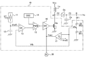
以下、本発明のスイッチング電源装置の実施例について、図1及び図2を参照して説明する。図1は、本発明の実施例に係るスイッチング電源装置の回路構成を示す図であり、図2はその動作を説明するための特性図である。 Embodiments of the switching power supply device of the present invention will be described below with reference to FIGS. FIG. 1 is a diagram showing a circuit configuration of a switching power supply device according to an embodiment of the present invention, and FIG. 2 is a characteristic diagram for explaining the operation thereof.
図1において、電源入力電圧Vccとグランド間にコイルLoとスイッチ手段Qoとが直列に接続される。スイッチ手段Qoは、MOSトランジスタやバイポーラトランジスタが好適である。この例では、スイッチ手段Qoとして、N型MOSトランジスタが使用されている。 In FIG. 1, a coil Lo and a switch means Qo are connected in series between a power supply input voltage Vcc and ground. The switch means Qo is preferably a MOS transistor or a bipolar transistor. In this example, an N-type MOS transistor is used as the switch means Qo.
そのコイルLoとスイッチ手段Qoとの直列接続点Aに整流用ダイオードDoのアノードが接続される。整流用ダイオードDoは電圧降下の小さいショットキ・バリヤ・ダイオードが好適である。その整流用ダイオードDoのカソードとグランド間に平滑用コンデンサCoが接続される。これにより、直列接続点Aの電圧が、整流用ダイオードDoと平滑用コンデンサCoからなる整流平滑回路で、整流平滑されて出力点Bから出力電圧Voとして、負荷(図示していない)に供給される。 The anode of the rectifying diode Do is connected to a series connection point A between the coil Lo and the switch means Qo. The rectifying diode Do is preferably a Schottky barrier diode with a small voltage drop. A smoothing capacitor Co is connected between the cathode of the rectifying diode Do and the ground. As a result, the voltage at the series connection point A is rectified and smoothed by the rectifying and smoothing circuit including the rectifying diode Do and the smoothing capacitor Co, and supplied from the output point B to the load (not shown) as the output voltage Vo. The
これらコイルLo、ダイオードDo、コンデンサCoは外付け部品で構成されることが多く、スイッチ手段Qoを含む制御手段(スイッチング電源用IC)10とともに、スイッチング型の昇圧回路が構成される。スイッチ手段Qoのゲートに印加されるスイッチング信号のデューティ比に応じて、スイッチ手段Qoのオン期間とオフ期間が変更されて、電源入力電圧Vccが昇圧された出力電圧Voが出力される。 The coil Lo, the diode Do, and the capacitor Co are often constituted by external components, and a switching type booster circuit is constituted together with the control means (switching power supply IC) 10 including the switching means Qo. Depending on the duty ratio of the switching signal applied to the gate of the switch means Qo, the ON period and the OFF period of the switch means Qo are changed, and the output voltage Vo obtained by boosting the power input voltage Vcc is output.
また、この昇圧回路では、スイッチング信号が供給されないとき、即ちスイッチ手段Qoがオフ状態のときには、コイルLo、ダイオードDoを介して、コンデンサCoは略電源入力電圧Vccに近くまで充電される。具体的には、電源入力電圧VccからダイオードDoの降下電圧Vfを引いた電圧に充電される。ダイオードDoの降下電圧Vfは、ショットキーダイオードの場合には比較的小さく、例えば0.2〜0.4v程度である。 Further, in this booster circuit, when the switching signal is not supplied, that is, when the switch means Qo is in the OFF state, the capacitor Co is charged almost to the power supply input voltage Vcc through the coil Lo and the diode Do. Specifically, the battery is charged to a voltage obtained by subtracting the drop voltage Vf of the diode Do from the power supply input voltage Vcc. The drop voltage Vf of the diode Do is relatively small in the case of a Schottky diode, for example, about 0.2 to 0.4 v.
出力点Bから抵抗21(抵抗値R1)と抵抗22(抵抗値R2)の分圧回路で出力電圧Voが分圧されて、抵抗21と抵抗22との直列接続点から分圧電圧Vfb(=Vo×R1/(R1+R2))が得られる。この分圧電圧Vfbが、第1検出電圧である帰還電圧になり、また、第2検出電圧になる。 The output voltage Vo is divided from the output point B by the voltage dividing circuit of the resistor 21 (resistance value R1) and the resistor 22 (resistance value R2), and the divided voltage Vfb (= Vo × R1 / (R1 + R2)) is obtained. This divided voltage Vfb becomes a feedback voltage that is a first detection voltage, and also becomes a second detection voltage.
スイッチ手段Qo及び抵抗21、22は、スイッチング電源用IC10に形成されている。スイッチ手段Qo及び抵抗21、22を例えばディスクリート部品として、スイッチング電源用IC10の外部に設けることも出来る。スイッチング電源用IC10の外部にスイッチ手段Qo及び抵抗21、22を設けた場合には、スイッチング電源用IC10の耐電圧を低いものにすることが出来る。
The switch means Qo and the
スイッチング電源用IC10に形成されているその他の構成について、順次説明する。ソフトスタートの充電回路11がコンデンサ12と直列に接続されており、その接続点の電圧が第1基準電圧Vref1である。ソフトスタートの充電回路11は、例えば定電流源回路により構成されており、スタート信号STが印加されると動作を開始する。ソフトスタートの充電回路11の定電流回路から一定の電流がコンデンサ12に流れて、コンデンサ12の充電電圧、即ち第1基準電圧Vref1が緩やかに立ち上がっていく。第1基準電圧Vref1は、図示しない電圧制御回路による制御により、所定の電圧になった時点で一定値に保たれる。コンデンサ12は、スイッチング電源用IC10の外部に設けてもよい。
Other configurations formed in the switching power supply IC 10 will be sequentially described. The soft-start charging circuit 11 is connected in series with the
誤差増幅回路13は、第1基準電圧Vref1が正(+)入力端子に入力され、第1検出電圧である帰還電圧Vfbが負(−)入力端子に入力され、その二入力の差を増幅して誤差信号として出力する。
In the
発振回路14は、パルス幅変調に用いる三角波信号を発生する。三角波信号に代えて、鋸歯状波信号でも良い。パルス幅変調(PWM)回路15は、誤差増幅回路13からの誤差信号が+入力端子に入力され、発振回路14からの三角波信号が−入力端子に入力され、その二入力を比較して、PWM信号を発生する。
The
ドライバー回路16は、パルス幅変調回路15からのPWM信号を受けて、これに同期したスイッチング信号を形成し、スイッチ手段Qoのゲートに印加する。したがって、スイッチング信号は、PWM信号である。このドライバー回路16は、他の制御信号(故障検出信号Fdet)によって、その動作を行わせるか、あるいはその動作を停止させるかが制御される。これらソフトスタートの充電回路11、コンデンサ12、誤差増幅回路13、発振回路14、パルス幅変調回路15、ドライバー回路16は、抵抗21、抵抗22とともに、制御回路を構成する。
The
故障検出用比較器17は、第2検出電圧である帰還電圧Vfbと第2基準電圧Vref2とを比較し、帰還電圧Vfbが第2基準電圧Vref2より小さいときに故障検出信号Fdetを発生し、ドライバー回路16に上述の他の制御信号として供給する。第2基準電圧Vref2は、スイッチ手段Qoがオフ状態のときの帰還電圧Vfbより少し低い電圧になるように設定することがよい。即ち、第2基準電圧Vref2は、(Vcc−Vf)×R1/(R1+R2)より小さい電圧に設定される。また、故障検出用比較器17には、ヒステリシス特性を持たせておくと、出力電圧変動やノイズの影響を抑えられて良い。故障検出用比較器17は、抵抗21、抵抗22とともに、故障検出回路を構成する。なお、故障検出用比較器17に供給される第2検出電圧は、帰還電圧Vfbに代えて、抵抗22へ印加される印加電圧(即ち、出力電圧Vo)としても良い。
The
なお、故障検出信号Fdetは、ドライバー回路16に限らず、スイッチ手段Qoへのスイッチング信号が停止できれば良いから、制御回路中のいずれかの回路に供給するようにしてもよい。
Note that the failure detection signal Fdet is not limited to the
また、故障検出信号Fdetは、スイッチング電源用IC10の外部にも導出するように構成しても良い。この導出された故障検出信号Fdetは、外部に設けられた警報手段30に供給される。そして、故障検出信号Fdetが発生されたことを警報する。警報手段30としては、LEDなどの表示器やブザーなどで良い。
Moreover, the failure detection signal Fdet may be configured to be derived outside the switching
以上のように構成されるスイッチング電源装置の動作を、図1とともに図2を参照して説明する。なお、図2では、出力電圧Voや帰還電圧Vfbに含まれる電圧変動は省略している。 The operation of the switching power supply configured as described above will be described with reference to FIG. 2 together with FIG. In FIG. 2, voltage fluctuations included in the output voltage Vo and the feedback voltage Vfb are omitted.
まず、スタート信号STがソフトスタートの充電回路11に供給される以前、即ちスイッチング電源装置が休止状態にある場合には、第1基準電圧Vref1は零であり、スイッチ手段Qoにはスイッチング信号は供給されていない。したがって、スイッチ手段Qoはオフ状態にある。 First, before the start signal ST is supplied to the soft start charging circuit 11, that is, when the switching power supply device is in a dormant state, the first reference voltage Vref1 is zero and the switching signal is supplied to the switch means Qo. It has not been. Therefore, the switch means Qo is in an off state.
この場合に、電源入力電圧Vccは印加されているので、コイルLo、ダイオードDoを介してコンデンサCoが充電される。その充電電圧は、電源入力電圧VccからダイオードDoの降下電圧Vfを引いた電圧であり、ほぼ電源入力電圧Vccに近い値である。この充電電圧が、出力電圧Voとなっている。また、帰還電圧Vfbは出力電圧Voを抵抗R21,R22で分圧した電圧であり、第1基準電圧Vref1は零である。なお、第2基準電圧Vref2は常に一定の電圧である。 In this case, since the power supply input voltage Vcc is applied, the capacitor Co is charged via the coil Lo and the diode Do. The charging voltage is a voltage obtained by subtracting the drop voltage Vf of the diode Do from the power supply input voltage Vcc, and is a value substantially close to the power supply input voltage Vcc. This charging voltage is the output voltage Vo. The feedback voltage Vfb is a voltage obtained by dividing the output voltage Vo by the resistors R21 and R22, and the first reference voltage Vref1 is zero. The second reference voltage Vref2 is always a constant voltage.
時点t1で、スタート信号STがソフトスタートの充電回路11に供給されると、コンデンサ12が定電流で充電が開始され、第1基準電圧Vref1は徐々に上昇していく。第1基準電圧Vref1が、時点t2で帰還電圧Vfbを上回るようになると、誤差増幅回路13から誤差信号が出力され、その誤差信号と三角波信号とがパルス幅変調回路15で比較されてPWM信号を発生する。これにより、ドライバー回路16を介してスイッチ手段Qoにスイッチング信号が印加されて、出力電圧Voが上昇していく。
When the start signal ST is supplied to the soft start charging circuit 11 at time t1, the
第1基準電圧Vref1の上昇に連れて、出力電圧Vo及び帰還電圧Vfbが上昇していく。第1基準電圧Vref1は、所定の基準値に達した時点t3で、その上昇が終了し、以後その所定の基準値で一定に維持される。帰還電圧Vfbがこの第1基準電圧Vref1に一致するようにスイッチ手段Qoがスイッチング制御されるから、出力電圧Voもそれらに対応した所定の電圧に維持される。 As the first reference voltage Vref1 increases, the output voltage Vo and the feedback voltage Vfb increase. The rise of the first reference voltage Vref1 ends at the time point t3 when it reaches the predetermined reference value, and is thereafter kept constant at the predetermined reference value. Since the switching means Qo is switching-controlled so that the feedback voltage Vfb matches the first reference voltage Vref1, the output voltage Vo is also maintained at a predetermined voltage corresponding to them.
第2基準電圧Vref2は、スイッチ手段Qoがオフ状態のときの帰還電圧Vfbより低い電圧になるように設定されているから、休止状態から定常出力状態に掛けて帰還電圧Vfbを下回っている。したがって、故障検出用比較器17は、故障検出信号Fdetを出力することはない。
Since the second reference voltage Vref2 is set to be lower than the feedback voltage Vfb when the switch means Qo is in the off state, the second reference voltage Vref2 is lower than the feedback voltage Vfb from the rest state to the steady output state. Therefore, the
定常出力状態において、時点t4で例えば図1中の故障点F1で示すように、分圧抵抗R2への経路において、オープン故障(断線や接続不良等)が発生した場合を想定する。この場合には、その故障点F1でのオープン故障によって帰還電圧Vfbは零になる。 Assume that an open failure (disconnection, poor connection, etc.) occurs in the path to the voltage dividing resistor R2 at the time t4, for example, as indicated by a failure point F1 in FIG. In this case, the feedback voltage Vfb becomes zero due to an open failure at the failure point F1.
帰還電圧Vfbが零になると、制御回路では第1基準電圧Vref1に帰還電圧Vfbを近づけるようにスイッチ手段Qoへのスイッチング信号(PWM制御信号)のデューティ比を高めるように動作するから、出力電圧Voは図2の時点t4に破線で示すように急激に上昇しようとする。 When the feedback voltage Vfb becomes zero, the control circuit operates to increase the duty ratio of the switching signal (PWM control signal) to the switch means Qo so as to bring the feedback voltage Vfb closer to the first reference voltage Vref1. Tries to rise rapidly as shown by the broken line at time t4 in FIG.
しかし、本発明では、時点t4で帰還電圧Vfbが零になると、故障検出用比較器17において第2基準電圧Vref2が帰還電圧Vfbを上回るから故障検出信号Fdetが発生されて、ドライバー回路16に印加される。ドライバー回路16では、故障検出信号Fdetが印加されると、パルス幅変調回路15からのPWM信号をスイッチ手段Qoにスイッチング信号として供給することを直ちに停止(遮断)する。
However, in the present invention, when the feedback voltage Vfb becomes zero at time t4, the
時点t4で帰還電圧Vfbが零になってから、スイッチ手段Qoへのスイッチング信号の供給停止までに要する時間遅れはほとんどなく、実質上直ちに停止される。また、故障検出信号Fdetが発生されたことは、外部の警報手段30に通知されるから、表示や音による警報がなされる。 There is almost no time delay required until the supply of the switching signal to the switch means Qo is stopped after the feedback voltage Vfb becomes zero at the time t4, and it is stopped immediately. Further, since the external alarm means 30 is notified that the failure detection signal Fdet has been generated, an alarm by display or sound is made.
これにより、出力電圧Voは、図2の時点t4に破線で示すように急激に上昇することはなく、逆に図2に実線で示すように逆に時点t4から低下していくことになる。したがって、出力電圧の異常な上昇(即ち、過電圧の発生)を未然に抑制できる。よって、出力電圧Voが供給される負荷のみでなく、スイッチング電源用IC10を耐電圧の低いものも使用することが出来る。また、警報手段30による警報によって、故障発生を報知することが出来るから、故障原因の調査が容易になる。
As a result, the output voltage Vo does not rapidly increase as indicated by a broken line at time t4 in FIG. 2, but conversely decreases from time t4 as indicated by a solid line in FIG. Therefore, an abnormal increase in output voltage (that is, occurrence of overvoltage) can be suppressed in advance. Therefore, not only the load to which the output voltage Vo is supplied but also the switching
また、スタート信号STが印加される時点で、既に故障点F1でオープン故障が発生している場合には、故障検出用比較器17から故障検出信号Fdetが出力されているから、ドライバー回路30はその動作が停止されている。したがって、スイッチ手段Qoにスイッチング信号が供給されることはない。この場合も、警報手段30による警報によって、故障発生を認識できる。
When an open failure has already occurred at the failure point F1 when the start signal ST is applied, the failure detection signal Fdet is output from the
このオープン故障の個所は、図1中の故障点F1に限らず、ダイオードDoのカソードから抵抗R2の接続点B間(例えば故障点F3の故障)のどこでも、また、接続点AとダイオードDoのアノード間(例えば故障点F2の故障)のどこであっても、故障点F1でのオープン故障の場合と同様に動作して、過電圧の発生を未然に抑制できる。したがって、オープン故障としては、経路中の断線や、ダイオードDo等構成素子の実装不良等幅広い故障に対応することが出来る。また、出力回路が短絡したような場合であっても、オープン故障の場合と同様に動作して、過電流を抑制することができる。また、以上の説明では、定常出力状態時やスタート前に故障が発生した場合について説明したが、スタート後の出力電圧の上昇中においても同様に動作する。 The location of the open failure is not limited to the failure point F1 in FIG. 1, but anywhere between the cathode of the diode Do and the connection point B of the resistor R2 (for example, failure of the failure point F3), and between the connection point A and the diode Do. The operation between the anodes (for example, failure at the failure point F2) can be performed in the same manner as in the case of the open failure at the failure point F1, and the occurrence of overvoltage can be suppressed in advance. Therefore, as an open failure, it is possible to deal with a wide range of failures such as disconnection in the path and mounting failure of components such as the diode Do. Further, even when the output circuit is short-circuited, the overcurrent can be suppressed by operating similarly to the case of the open failure. In the above description, the case where a failure occurs in the steady output state or before the start has been described. However, the same operation is performed even when the output voltage rises after the start.
なお、昇圧回路としては、電源入力電圧をスイッチング信号に応じて昇圧し、昇圧された出力電圧を出力するとともに、スイッチング信号が供給されない時に電源入力電圧に略近い電圧を出力電圧として出力する昇圧回路であればよい。例えば、チャージポンプ型の昇圧回路にも適用できる。また、ソフトスタートの充電回路11として、定電流回路のみを示したが、これに限定されない。 The booster circuit boosts the power supply input voltage according to the switching signal, outputs the boosted output voltage, and outputs a voltage substantially close to the power supply input voltage as the output voltage when the switching signal is not supplied. If it is. For example, the present invention can be applied to a charge pump type booster circuit. Further, although only the constant current circuit is shown as the soft start charging circuit 11, it is not limited to this.
Lo コイル
Qo スイッチ手段
Do 整流用ダイオード
Co 平滑用コンデンサ
Vcc 電源入力電圧
Vo 出力電圧
10 スイッチング電源用IC
11 ソフトスタートの充電回路
12 コンデンサ
13 誤差増幅回路
14 発振回路
15 パルス幅変調回路
16 ドライバー回路
17 故障検出用比較器
21、22 分圧抵抗
30 警報手段
Vref1 第1基準電圧
Vref2 第2基準電圧
Vfb 帰還電圧
Fdet 故障検出信号
ST スタート信号
F1〜F3 故障点
Lo Coil Qo Switch means Do Rectifier diode Co Smoothing capacitor Vcc Power supply input voltage
11 Soft start charging
Claims (7)
前記出力電圧に応じて検出されるべき第1検出電圧と第1基準電圧とが入力され、前記第1検出電圧が前記第1基準電圧に等しくなるように、前記第1検出電圧と前記第1基準電圧との差電圧に応じて制御された前記スイッチング信号を出力する制御回路と、
前記出力電圧に応じて検出されるべき第2検出電圧と第2基準電圧とを比較し、前記第2基準電圧が前記第2検出電圧を上回った時に前記スイッチング信号の供給を停止させるための故障検出信号を発生し、前記制御回路に入力する故障検出回路と、を有することを特徴とする、スイッチング型電源装置。 A booster circuit that boosts a power supply input voltage in accordance with a switching signal, outputs a boosted output voltage, and outputs a voltage substantially close to the power supply input voltage when the switching signal is not supplied;
The first detection voltage and the first reference voltage to be detected according to the output voltage are input, and the first detection voltage and the first reference voltage are equal to the first reference voltage. A control circuit that outputs the switching signal controlled in accordance with a voltage difference from a reference voltage;
A failure for comparing the second detection voltage to be detected according to the output voltage with a second reference voltage and stopping the supply of the switching signal when the second reference voltage exceeds the second detection voltage And a failure detection circuit which generates a detection signal and inputs the detection signal to the control circuit.
Priority Applications (7)
| Application Number | Priority Date | Filing Date | Title |
|---|---|---|---|
| JP2003349014A JP2005117784A (en) | 2003-10-08 | 2003-10-08 | Switching power supply apparatus |
| TW093129371A TW200520357A (en) | 2003-10-08 | 2004-09-29 | Switching power device |
| US10/959,018 US7301312B2 (en) | 2003-10-08 | 2004-10-04 | Switching power supply unit for generating an output voltage stepped up from an input voltage |
| KR1020040080000A KR20050033854A (en) | 2003-10-08 | 2004-10-07 | Switching power equipment |
| CNA2004100951361A CN1607715A (en) | 2003-10-08 | 2004-10-08 | Switching power supply unit |
| US11/764,055 US7471070B2 (en) | 2003-10-08 | 2007-06-15 | Switching power supply unit for generating an output voltage stepped up from an input voltage |
| US12/325,907 US7633274B2 (en) | 2003-10-08 | 2008-12-01 | Step-up switching power supply with open-circuit malfunction response |
Applications Claiming Priority (1)
| Application Number | Priority Date | Filing Date | Title |
|---|---|---|---|
| JP2003349014A JP2005117784A (en) | 2003-10-08 | 2003-10-08 | Switching power supply apparatus |
Publications (1)
| Publication Number | Publication Date |
|---|---|
| JP2005117784A true JP2005117784A (en) | 2005-04-28 |
Family
ID=34419683
Family Applications (1)
| Application Number | Title | Priority Date | Filing Date |
|---|---|---|---|
| JP2003349014A Pending JP2005117784A (en) | 2003-10-08 | 2003-10-08 | Switching power supply apparatus |
Country Status (5)
| Country | Link |
|---|---|
| US (3) | US7301312B2 (en) |
| JP (1) | JP2005117784A (en) |
| KR (1) | KR20050033854A (en) |
| CN (1) | CN1607715A (en) |
| TW (1) | TW200520357A (en) |
Cited By (13)
| Publication number | Priority date | Publication date | Assignee | Title |
|---|---|---|---|---|
| WO2007010802A1 (en) * | 2005-07-15 | 2007-01-25 | Rohm Co., Ltd. | Step-up switching regulator and its control circuit and electronic apparatus employing it |
| JP2007043861A (en) * | 2005-08-05 | 2007-02-15 | Rohm Co Ltd | Power supply and electric apparatus employing it |
| US7242170B1 (en) | 2006-01-09 | 2007-07-10 | Fujitsu Limited | Control circuit having error amplifier for DC-DC converter and control method therefor |
| US7586296B2 (en) | 2006-03-17 | 2009-09-08 | Denso Corporation | Power supply apparatus |
| JP2010017054A (en) * | 2008-07-07 | 2010-01-21 | Nissan Motor Co Ltd | Flyback switching supply |
| US7777474B2 (en) | 2006-06-09 | 2010-08-17 | Fujitsu Semiconductor Limited | DC-DC converter with oscillator and monitoring function |
| KR101077372B1 (en) | 2008-11-25 | 2011-10-26 | 가부시키가이샤 히타치 디스프레이즈 | Power circuit of display device and display device using the same |
| JP2015027196A (en) * | 2013-07-26 | 2015-02-05 | 新電元工業株式会社 | Bidirectional dc/dc converter device |
| KR20170002325A (en) * | 2015-06-29 | 2017-01-06 | 페어차일드코리아반도체 주식회사 | Soft-start circuit and buck converter comprising the same |
| JP2017107551A (en) * | 2015-11-30 | 2017-06-15 | ローム株式会社 | Power supply regulator |
| KR101904717B1 (en) * | 2018-02-12 | 2018-10-05 | 엘지디스플레이 주식회사 | Apparatus for protecting a light emitting diode and liquid crystal display using the same |
| JP2020102083A (en) * | 2018-12-25 | 2020-07-02 | 株式会社デンソーテン | Voltage conversion apparatus |
| US10886842B2 (en) | 2019-03-15 | 2021-01-05 | Kabushiki Kaisha Toshiba | Power supply circuit and control method for power supply circuit |
Families Citing this family (39)
| Publication number | Priority date | Publication date | Assignee | Title |
|---|---|---|---|---|
| JP2005117784A (en) * | 2003-10-08 | 2005-04-28 | Rohm Co Ltd | Switching power supply apparatus |
| US7579784B2 (en) * | 2004-12-03 | 2009-08-25 | Rohm Co., Ltd. | Switching power supply and its control circuit, and electronic apparatus employing such switching power supply |
| JP4172473B2 (en) * | 2005-06-29 | 2008-10-29 | オムロン株式会社 | Booster circuit and electric power steering device |
| US7539028B2 (en) * | 2005-07-01 | 2009-05-26 | Power Integrations, Inc. | Method and apparatus for fault detection in a switching power supply |
| JP4823604B2 (en) * | 2005-08-05 | 2011-11-24 | ローム株式会社 | Soft start circuit, power supply, electrical equipment |
| TWI279955B (en) * | 2005-09-09 | 2007-04-21 | Realtek Semiconductor Corp | Switching regulator with over-current protection |
| JP2007202273A (en) * | 2006-01-25 | 2007-08-09 | Ricoh Co Ltd | Switching regulator |
| KR100809688B1 (en) * | 2006-03-31 | 2008-03-06 | 삼성전자주식회사 | Over voltage protection circuit and method thereof |
| JP4338721B2 (en) * | 2006-08-22 | 2009-10-07 | 株式会社日立製作所 | Power conversion apparatus and abnormality detection method thereof |
| TW200910044A (en) * | 2007-08-24 | 2009-03-01 | Vastview Tech Inc | Constant current regulating circuit with a current sensing loop |
| CN101394700B (en) * | 2007-09-17 | 2012-10-17 | 钰瀚科技股份有限公司 | Constant current regulating circuit having current sensing loop |
| US20090115390A1 (en) * | 2007-11-05 | 2009-05-07 | Chen-Min Chen | Power converter with protection mechanism for diode in open-circuit condition and pulse-width-modulation controller thereof |
| KR100806295B1 (en) * | 2007-11-26 | 2008-02-22 | 주식회사 룩센테크놀러지 | Output voltage adaptive converter and method thereof |
| JP5076993B2 (en) * | 2008-03-19 | 2012-11-21 | 富士電機株式会社 | Switching power supply |
| JP5091024B2 (en) * | 2008-06-24 | 2012-12-05 | 株式会社リコー | Switching regulator and operation control method thereof |
| TWI380548B (en) * | 2008-12-16 | 2012-12-21 | Delta Electronics Inc | Error detecting and motor protecting apparatus and method thereof |
| KR101387279B1 (en) * | 2009-07-31 | 2014-04-18 | 다이킨 고교 가부시키가이샤 | Power conversion device |
| US8179156B2 (en) * | 2009-11-19 | 2012-05-15 | Semiconductor Components Industries, Llc | Capacitor test method and circuit therefor |
| CN102130574B (en) * | 2010-01-13 | 2013-06-19 | 台达电子工业股份有限公司 | Multi-output voltage-reduction type conversion device with controllable energy release function |
| JP2011244677A (en) * | 2010-04-23 | 2011-12-01 | Rohm Co Ltd | Control circuit for switching power supply, and switching power supply, light-emitting device and electronic apparatus with the same |
| CN104967110B (en) * | 2011-02-22 | 2018-03-23 | 台达电子工业股份有限公司 | More power sources in parallel electric power systems |
| TWI429162B (en) | 2011-02-22 | 2014-03-01 | Delta Electronics Inc | A power supply system with multiple power sources in parallel |
| CN103259243B (en) * | 2012-02-16 | 2016-01-13 | 佳能株式会社 | Information processor and control method thereof |
| CN103904767B (en) * | 2012-12-28 | 2016-02-17 | 台达电子工业股份有限公司 | UPS and method of operation thereof |
| US9285812B2 (en) * | 2013-02-01 | 2016-03-15 | Allegro Microsystems, Llc | Soft start circuits and techniques |
| TWI497883B (en) * | 2013-08-14 | 2015-08-21 | Beyond Innovation Tech Co Ltd | Boost apparatus with over-current and over-voltage protection function |
| CN103683931B (en) * | 2013-12-27 | 2016-09-28 | 深圳市航嘉驰源电气股份有限公司 | A kind of power-switching circuit |
| CN105373178B (en) * | 2014-08-15 | 2018-02-02 | 深圳市中兴微电子技术有限公司 | Circuit start method, control circuit and voltage reference circuit |
| CN104410299A (en) * | 2014-11-23 | 2015-03-11 | 成都创图科技有限公司 | Double-buffering trigger type driving power source for power system fault detecting device |
| CN104507215B (en) * | 2014-12-04 | 2018-05-04 | 苏州工业园区海的机电科技有限公司 | LED module lights detection device and its lights detection method |
| JP2016140118A (en) * | 2015-01-26 | 2016-08-04 | 株式会社村田製作所 | Power supply |
| CN108528051B (en) * | 2017-03-06 | 2020-09-25 | 珠海天威技术开发有限公司 | Power supply voltage control circuit and working method thereof, consumable chip and working method thereof |
| CN106953300B (en) * | 2017-04-14 | 2019-04-16 | 深圳创维-Rgb电子有限公司 | A kind of protective circuit of switch power source and display equipment |
| CN107147082B (en) * | 2017-06-20 | 2019-04-19 | 矽力杰半导体技术(杭州)有限公司 | Overvoltage crowbar and the integrated circuit and switch converters for applying it |
| US10256623B2 (en) | 2017-08-21 | 2019-04-09 | Rohm Co., Ltd. | Power control device |
| JP2019129607A (en) * | 2018-01-24 | 2019-08-01 | トヨタ自動車株式会社 | Power supply controller |
| JP6809489B2 (en) | 2018-01-25 | 2021-01-06 | 株式会社デンソー | Boost switching power supply circuit |
| CN111366804B (en) * | 2020-03-25 | 2022-07-19 | 广州华凌制冷设备有限公司 | Power supply circuit, circuit fault detection method, circuit board and vehicle-mounted air conditioner |
| DE102021206136A1 (en) * | 2021-06-16 | 2022-12-22 | Robert Bosch Gesellschaft mit beschränkter Haftung | voltage regulator |
Citations (3)
| Publication number | Priority date | Publication date | Assignee | Title |
|---|---|---|---|---|
| JPH0284056A (en) * | 1988-09-17 | 1990-03-26 | Fuji Electric Co Ltd | Output voltage control method for booster chopper apparatus |
| JPH06311733A (en) * | 1993-04-21 | 1994-11-04 | Fujitsu Ten Ltd | Malfunction detector in booster circuit |
| JP2000032743A (en) * | 1998-07-09 | 2000-01-28 | Matsushita Electric Works Ltd | Power unit |
Family Cites Families (6)
| Publication number | Priority date | Publication date | Assignee | Title |
|---|---|---|---|---|
| US5359281A (en) * | 1992-06-08 | 1994-10-25 | Motorola, Inc. | Quick-start and overvoltage protection for a switching regulator circuit |
| US6185082B1 (en) * | 1999-06-01 | 2001-02-06 | System General Corporation | Protection circuit for a boost power converter |
| JP3610830B2 (en) | 1999-06-16 | 2005-01-19 | 富士ゼロックス株式会社 | Power supply |
| JP4397617B2 (en) * | 2003-04-01 | 2010-01-13 | パナソニック株式会社 | Multi-output DC-DC converter |
| US6936997B2 (en) * | 2003-08-11 | 2005-08-30 | Semiconductor Components Industries, Llc | Method of forming a high efficiency power controller |
| JP2005117784A (en) * | 2003-10-08 | 2005-04-28 | Rohm Co Ltd | Switching power supply apparatus |
-
2003
- 2003-10-08 JP JP2003349014A patent/JP2005117784A/en active Pending
-
2004
- 2004-09-29 TW TW093129371A patent/TW200520357A/en unknown
- 2004-10-04 US US10/959,018 patent/US7301312B2/en active Active
- 2004-10-07 KR KR1020040080000A patent/KR20050033854A/en not_active Application Discontinuation
- 2004-10-08 CN CNA2004100951361A patent/CN1607715A/en active Pending
-
2007
- 2007-06-15 US US11/764,055 patent/US7471070B2/en active Active
-
2008
- 2008-12-01 US US12/325,907 patent/US7633274B2/en active Active
Patent Citations (3)
| Publication number | Priority date | Publication date | Assignee | Title |
|---|---|---|---|---|
| JPH0284056A (en) * | 1988-09-17 | 1990-03-26 | Fuji Electric Co Ltd | Output voltage control method for booster chopper apparatus |
| JPH06311733A (en) * | 1993-04-21 | 1994-11-04 | Fujitsu Ten Ltd | Malfunction detector in booster circuit |
| JP2000032743A (en) * | 1998-07-09 | 2000-01-28 | Matsushita Electric Works Ltd | Power unit |
Cited By (19)
| Publication number | Priority date | Publication date | Assignee | Title |
|---|---|---|---|---|
| WO2007010802A1 (en) * | 2005-07-15 | 2007-01-25 | Rohm Co., Ltd. | Step-up switching regulator and its control circuit and electronic apparatus employing it |
| JP2007028783A (en) * | 2005-07-15 | 2007-02-01 | Rohm Co Ltd | Step-up switching regulator, its control circuit and electronic apparatus employing the circuit |
| US7755340B2 (en) | 2005-07-15 | 2010-07-13 | Rohm Co., Ltd. | Step-up switching regulator with soft start circuits |
| JP2007043861A (en) * | 2005-08-05 | 2007-02-15 | Rohm Co Ltd | Power supply and electric apparatus employing it |
| WO2007018089A1 (en) * | 2005-08-05 | 2007-02-15 | Rohm Co., Ltd. | Power supply device and electric device using the same |
| US7893667B2 (en) | 2005-08-05 | 2011-02-22 | Rohm Co., Ltd. | PWM power supply apparatus having a controlled duty ratio without causing overall system oscillation |
| US7242170B1 (en) | 2006-01-09 | 2007-07-10 | Fujitsu Limited | Control circuit having error amplifier for DC-DC converter and control method therefor |
| US7586296B2 (en) | 2006-03-17 | 2009-09-08 | Denso Corporation | Power supply apparatus |
| US7777474B2 (en) | 2006-06-09 | 2010-08-17 | Fujitsu Semiconductor Limited | DC-DC converter with oscillator and monitoring function |
| JP2010017054A (en) * | 2008-07-07 | 2010-01-21 | Nissan Motor Co Ltd | Flyback switching supply |
| KR101077372B1 (en) | 2008-11-25 | 2011-10-26 | 가부시키가이샤 히타치 디스프레이즈 | Power circuit of display device and display device using the same |
| JP2015027196A (en) * | 2013-07-26 | 2015-02-05 | 新電元工業株式会社 | Bidirectional dc/dc converter device |
| KR20170002325A (en) * | 2015-06-29 | 2017-01-06 | 페어차일드코리아반도체 주식회사 | Soft-start circuit and buck converter comprising the same |
| KR102231095B1 (en) | 2015-06-29 | 2021-03-22 | 온세미컨덕터코리아 주식회사 | Soft-start circuit and buck converter comprising the same |
| JP2017107551A (en) * | 2015-11-30 | 2017-06-15 | ローム株式会社 | Power supply regulator |
| KR101904717B1 (en) * | 2018-02-12 | 2018-10-05 | 엘지디스플레이 주식회사 | Apparatus for protecting a light emitting diode and liquid crystal display using the same |
| JP2020102083A (en) * | 2018-12-25 | 2020-07-02 | 株式会社デンソーテン | Voltage conversion apparatus |
| JP7133463B2 (en) | 2018-12-25 | 2022-09-08 | 株式会社デンソーテン | voltage converter |
| US10886842B2 (en) | 2019-03-15 | 2021-01-05 | Kabushiki Kaisha Toshiba | Power supply circuit and control method for power supply circuit |
Also Published As
| Publication number | Publication date |
|---|---|
| US7633274B2 (en) | 2009-12-15 |
| US20080030173A1 (en) | 2008-02-07 |
| US20090085547A1 (en) | 2009-04-02 |
| US7471070B2 (en) | 2008-12-30 |
| KR20050033854A (en) | 2005-04-13 |
| CN1607715A (en) | 2005-04-20 |
| US7301312B2 (en) | 2007-11-27 |
| US20050077882A1 (en) | 2005-04-14 |
| TW200520357A (en) | 2005-06-16 |
| TWI350637B (en) | 2011-10-11 |
Similar Documents
| Publication | Publication Date | Title |
|---|---|---|
| JP2005117784A (en) | Switching power supply apparatus | |
| US7071667B2 (en) | DC—DC converter | |
| JP4912067B2 (en) | Semiconductor integrated circuit and electronic device having the same | |
| KR102110109B1 (en) | Switching regulator and electronic device | |
| JP2005117810A (en) | Switching power supply device and electronic apparatus equipped with indication device | |
| JP2012060714A (en) | Integrated circuit | |
| JP2007089239A (en) | Dc-dc converter with short circuit protection circuit | |
| KR20060135559A (en) | Switching control circuit and self-excited dc-dc converter | |
| JP2009153234A (en) | Switching power supply device | |
| JP5091024B2 (en) | Switching regulator and operation control method thereof | |
| JP5228567B2 (en) | Boost DC-DC converter | |
| JP5254876B2 (en) | Power factor improved switching power supply | |
| US8492993B2 (en) | LED driving circuit and power converting circuit | |
| JP2015162939A (en) | Dc/dc converter and control method therefor | |
| JP2009148030A (en) | Power controller and machine using it | |
| JPH05251800A (en) | He-ne laser power supply | |
| JP6109976B1 (en) | Automatic voltage regulator | |
| JP2009290937A (en) | Switching power supply | |
| JP2019022303A (en) | Dc/dc converter and control circuit of the same | |
| JP6344086B2 (en) | Control device | |
| JP5338159B2 (en) | Flyback switching power supply | |
| JP4957041B2 (en) | Power supply device | |
| JP2014197941A (en) | Power conversion device and inrush current suppression method | |
| JP6372189B2 (en) | Control device | |
| JP2010124648A (en) | Switching power supply apparatus |
Legal Events
| Date | Code | Title | Description |
|---|---|---|---|
| A621 | Written request for application examination |
Free format text: JAPANESE INTERMEDIATE CODE: A621 Effective date: 20060810 |
|
| RD03 | Notification of appointment of power of attorney |
Free format text: JAPANESE INTERMEDIATE CODE: A7423 Effective date: 20090122 |
|
| RD04 | Notification of resignation of power of attorney |
Free format text: JAPANESE INTERMEDIATE CODE: A7424 Effective date: 20090210 |
|
| A977 | Report on retrieval |
Free format text: JAPANESE INTERMEDIATE CODE: A971007 Effective date: 20090409 |
|
| A131 | Notification of reasons for refusal |
Free format text: JAPANESE INTERMEDIATE CODE: A131 Effective date: 20090421 |
|
| A521 | Request for written amendment filed |
Free format text: JAPANESE INTERMEDIATE CODE: A523 Effective date: 20090622 |
|
| A131 | Notification of reasons for refusal |
Free format text: JAPANESE INTERMEDIATE CODE: A131 Effective date: 20091117 |
|
| A02 | Decision of refusal |
Free format text: JAPANESE INTERMEDIATE CODE: A02 Effective date: 20100316 |