CN1183807C - Process for producing voltage pulse sequences and circuit assembly therefor - Google Patents
Process for producing voltage pulse sequences and circuit assembly therefor Download PDFInfo
- Publication number
- CN1183807C CN1183807C CNB988010321A CN98801032A CN1183807C CN 1183807 C CN1183807 C CN 1183807C CN B988010321 A CNB988010321 A CN B988010321A CN 98801032 A CN98801032 A CN 98801032A CN 1183807 C CN1183807 C CN 1183807C
- Authority
- CN
- China
- Prior art keywords
- switch
- illuminator
- dielectric isolation
- voltage
- pulse
- Prior art date
- Legal status (The legal status is an assumption and is not a legal conclusion. Google has not performed a legal analysis and makes no representation as to the accuracy of the status listed.)
- Expired - Lifetime
Links
Images


Classifications
-
- H—ELECTRICITY
- H05—ELECTRIC TECHNIQUES NOT OTHERWISE PROVIDED FOR
- H05B—ELECTRIC HEATING; ELECTRIC LIGHT SOURCES NOT OTHERWISE PROVIDED FOR; CIRCUIT ARRANGEMENTS FOR ELECTRIC LIGHT SOURCES, IN GENERAL
- H05B41/00—Circuit arrangements or apparatus for igniting or operating discharge lamps
- H05B41/14—Circuit arrangements
- H05B41/26—Circuit arrangements in which the lamp is fed by power derived from dc by means of a converter, e.g. by high-voltage dc
- H05B41/28—Circuit arrangements in which the lamp is fed by power derived from dc by means of a converter, e.g. by high-voltage dc using static converters
- H05B41/288—Circuit arrangements in which the lamp is fed by power derived from dc by means of a converter, e.g. by high-voltage dc using static converters with semiconductor devices and specially adapted for lamps without preheating electrodes, e.g. for high-intensity discharge lamps, high-pressure mercury or sodium lamps or low-pressure sodium lamps
- H05B41/2881—Load circuits; Control thereof
-
- H—ELECTRICITY
- H05—ELECTRIC TECHNIQUES NOT OTHERWISE PROVIDED FOR
- H05B—ELECTRIC HEATING; ELECTRIC LIGHT SOURCES NOT OTHERWISE PROVIDED FOR; CIRCUIT ARRANGEMENTS FOR ELECTRIC LIGHT SOURCES, IN GENERAL
- H05B41/00—Circuit arrangements or apparatus for igniting or operating discharge lamps
- H05B41/14—Circuit arrangements
- H05B41/30—Circuit arrangements in which the lamp is fed by pulses, e.g. flash lamp
-
- H—ELECTRICITY
- H05—ELECTRIC TECHNIQUES NOT OTHERWISE PROVIDED FOR
- H05B—ELECTRIC HEATING; ELECTRIC LIGHT SOURCES NOT OTHERWISE PROVIDED FOR; CIRCUIT ARRANGEMENTS FOR ELECTRIC LIGHT SOURCES, IN GENERAL
- H05B41/00—Circuit arrangements or apparatus for igniting or operating discharge lamps
- H05B41/14—Circuit arrangements
- H05B41/26—Circuit arrangements in which the lamp is fed by power derived from dc by means of a converter, e.g. by high-voltage dc
- H05B41/28—Circuit arrangements in which the lamp is fed by power derived from dc by means of a converter, e.g. by high-voltage dc using static converters
- H05B41/2806—Circuit arrangements in which the lamp is fed by power derived from dc by means of a converter, e.g. by high-voltage dc using static converters with semiconductor devices and specially adapted for lamps without electrodes in the vessel, e.g. surface discharge lamps, electrodeless discharge lamps
-
- Y—GENERAL TAGGING OF NEW TECHNOLOGICAL DEVELOPMENTS; GENERAL TAGGING OF CROSS-SECTIONAL TECHNOLOGIES SPANNING OVER SEVERAL SECTIONS OF THE IPC; TECHNICAL SUBJECTS COVERED BY FORMER USPC CROSS-REFERENCE ART COLLECTIONS [XRACs] AND DIGESTS
- Y02—TECHNOLOGIES OR APPLICATIONS FOR MITIGATION OR ADAPTATION AGAINST CLIMATE CHANGE
- Y02B—CLIMATE CHANGE MITIGATION TECHNOLOGIES RELATED TO BUILDINGS, e.g. HOUSING, HOUSE APPLIANCES OR RELATED END-USER APPLICATIONS
- Y02B20/00—Energy efficient lighting technologies, e.g. halogen lamps or gas discharge lamps
-
- Y—GENERAL TAGGING OF NEW TECHNOLOGICAL DEVELOPMENTS; GENERAL TAGGING OF CROSS-SECTIONAL TECHNOLOGIES SPANNING OVER SEVERAL SECTIONS OF THE IPC; TECHNICAL SUBJECTS COVERED BY FORMER USPC CROSS-REFERENCE ART COLLECTIONS [XRACs] AND DIGESTS
- Y10—TECHNICAL SUBJECTS COVERED BY FORMER USPC
- Y10S—TECHNICAL SUBJECTS COVERED BY FORMER USPC CROSS-REFERENCE ART COLLECTIONS [XRACs] AND DIGESTS
- Y10S315/00—Electric lamp and discharge devices: systems
- Y10S315/07—Starting and control circuits for gas discharge lamp using transistors
Abstract
An electric circuit assembly for generating voltage pulse sequences for the operation of dielectrically inhibited discharges, comprising a series circuit provided with an oscillating circuit induction coil (TR2-A) and a controlled switch (T1), a pulse generator (OS) controlling said switch (T1), a current valve (D1) mounted in parallel to said switch (T1), a feedback capacitor (C2) also mounted in parallel to said switch (T1), an element for coupling a lamp (La1) to at least one dielectrically inhibited electrode and optionally a feedback buffer capacitor (C1) mounted in parallel to said series circuit provided with said oscillating circuit induction coil (TR2-A) and said controlled switch (T1). The coupling element of a lamp particularly includes two terminals (a'', b'') and the secondary winding (TR2-B) of an autotransformer (TR2) mounted between a first pole of said switch (T1) and the associated terminal (a''), wherein the primary winding (TR2-A) of said autotransformer (TR2) acts as an oscillating circuit induction coil. The second terminal (b'') is connected to the second pole of said switch (T1). In operation, said switch (T1) opens and closes alternately according to the control signal rate of the pulse generator (OS), in order to generate a sequence of voltage pulses separated by interruption times at the dielectrically inhibited electrodes of a lamp connected to the terminals (a'', b'').
Description
Technical field
The present invention relates to a kind of circuit arrangement.It relates to a kind of circuit arrangement that is used to drive the pulse voltage series of discharge lamp.The present invention relates to produce the method for pulse voltage series in addition by this circuit arrangement.
More properly, the present invention relates to drive the circuit arrangement of discharge lamp or light source, wherein the electrode of at least one polarity of discharge lamp is a dielectric isolation, this circuit arrangement by unipolarity or at least essence be that unipolar potential pulse drives discharge lamp, described in WO 94/23442.Unconfined sequence of voltage pulses on this type of drive using priciple, they were separated each other by the dead zone time.The luminous essence that plays a decisive role is pulse shape and pulse duration and dead zone time for producing effectively efficiently.Usually in the scope of conduction ratio between about 1: 5 to 1: 10.The peak value of high-voltage pulse is relevant with corresponding modulated structure, and for example with electrode number, arcing distance and media type and thickness are relevant, usually between 1KV and 5KV.Pulse repetition frequency is relevant with the geometric parameter of lamp simultaneously, reaches at about 25KHz to the scope of about 80KHz.Conventional ADS driving mode for this lamp then is to use sinusoidal shape alternating voltage.
Dielectric isolation discharge is different from the discharge of carrying out in the common discharge lamp, and it has one or more electrodes (one-sided dielectric isolation) of being located at the inner and same polarity of discharge space or all electrodes is medium between the dipolar electrode (bilateral dielectric isolation).Kind electrode is also referred to as dielectric isolation electrode.Electric charge from a dielectric isolation electrode to discharge section ionized gas moves so not by conductor current but realize by capacitance current.In the equivalent circuit diagram of this electric discharge device, produced capacitive element thus.Therefore this circuit arrangement must adapt to the energy capacitive be coupled in the discharge lamp.
Background technology
By DE 195 48 003 A1 known a kind of generation pulse voltage series, especially drive the circuit arrangement of dielectric isolation electric discharge device.It has: one with charge circuit input voltage power supply and that have charging capacitor; Discharge and a pulse circuit with fast controllable switch, it is connected with a pulse control circuit; Impulser that has a coupled load and one have the feedback current valve and import the feedback tank circuit of buffer condenser in parallel with charge circuit.During each switch conduction, the electric energy that is stored in the capacitor is sent to load by impulser.Storing feedback energy storage point by the energy of load and impulser feedback into by the feedback tank circuit goes up and is cushioned capacitor and absorb.Thus on the current potential of the voltage clamp that makes secondary winding during the feedback at input voltage.In addition, feedback energy can be common to charging stage of charging capacitor in this way.The shortcoming of this scheme is the high impulse load of impulser and switch element, and this causes the efficient and the big relatively element cost of relative mistake.In addition, the concrete structure of impulser has significant impact to switching function.The optimum structure of impulser only can be definite by testing.
Summary of the invention
Task of the present invention is, a kind of circuit arrangement is provided, and can produce essence with less switching loss by it is unipolar pulse voltage series.This pulse voltage series should be accomplished and have level and smooth as far as possible pulse shape in the load of essence capacitive effect in addition.Another aspect of the present invention is to realize simple relatively circuit with few relatively element.
This task will solve by feature of the present invention.According to illuminator of the present invention, have
A pulse voltage source, it is suitable for providing at work the potential pulse of being separated by time out,
The discharge lamp of a dielectric isolation (La1) has
One is partially transparent at least and that be filled with air seal or can be flow through and open discharge vessel by gas or admixture of gas, and it is made by electrically non-conductive material, and
Electrode, it is connected with pulse voltage source, and wherein the electrode of at least one polarity separates by dielectric material and discharge vessel inside,
And wherein, this pulse voltage source has a circuit arrangement that is used to produce pulse voltage series, and these pulse voltage series are used to operate the interior dielectric isolation discharge of discharge vessel of the discharge lamp (La1) of dielectric isolation, have
A tanke circuit inductance (L1; TR1-A, TR2-A),
A gate-controlled switch (T1, T2), it and tanke circuit inductance (L1; TR1-A; TR2-A) series connection,
A pulse generator (OS), its control switch (T1),
A current valve (D1), it and switch (T1) inverse parallel, wherein, this current valve is by a hidden element or plays integrated source-leakages diode formation of the MOSFET (T2) of on-off action,
A tank circuit inductance (C2), it is in parallel with switch (T1), wherein, tank circuit inductance be by a hidden element or partly the natural capacity of the discharge lamp (La1) of the barrier layer electric capacity by a MOSFET (T2) who plays on-off action and/or this dielectric isolation of joining form
Device (a, a b who is used to connect the discharge lamp (La1) of this dielectric isolation; TR1-B, a ' b '; TR2-B, a ", b "),
Wherein, control signal by pulse generator (OS) when work alternately makes switch (T1, T2) conducting or blocking-up produce the sequence of voltage pulses that is suspended time-division thus between the electrode of the discharge lamp (La1) of a dielectric isolation that is connected with this device.Its particularly advantageous configuration provides below.
Another task of the present invention is to provide a kind of method that produces above-mentioned pulse voltage series.This task will solve by method feature described later.
Basic design of the present invention will following by Fig. 1 in simplified block diagram explain., at first perceptual accumulator 3 is loaded periodically by 1 power supply of an energy supply source in gate-controlled switch 2 conducting phase.In case after loading, i.e. switch 2 blocking-up, the magnetic energy of storage will be sent in the capacitive accumulator 4 in perceptual accumulator 3.On perceptual accumulator 3, produce the first voltage half-wave of a pure oscillation thus, and on capacitive accumulator 4, also produce identical voltage half-wave, but its phase place is opposite.The first voltage half-wave is used as the potential pulse of lamp 5, it or be coupling on the inductance 3 or be coupling on the capacitive accumulator 4.Then, the energy on the capacitive accumulator 4 feeds back in the energy supply source 1 by perceptual accumulator 3, and the latter preferably includes an additional feedback accumulator (not shown).In the case, the voltage on the capacitive accumulator 4 by nip on voltage by 6 landing of the current valve opened.Therefore, the voltage on the perceptual during this period accumulator 3 equals supply power voltage.After preset time, repeat this process periodically.This timing controlled realizes by a signal generator 7 that is connected with gate-controlled switch 2.
In this way, produce homophase, being connected to essence on the lamp electrode is the potential pulse of the sinusoidal shape of half-wave, and wherein each potential pulse separated each other by the dead zone time, and this dead zone time is that the electrode compacting matter that powers on is constant and is significantly less than the potential pulse peak value, preferably is about time of null value.
The core of the present invention design is to solve by the inductance (hereinafter to be referred as tanke circuit inductance) that at first uses as the inductive energy storage device and the series circuit of a gate-controlled switch, wherein to switch in parallel electric capacity-be designated hereinafter simply as tank circuit inductance-and current valve as the capacitive accumulator.
Can at first influence the width of potential pulse by the occurrence of getting for tanke circuit inductance and tank circuit inductance.For the driving of the described types of light sources of beginning part, tanke circuit inductance is between about 500 μ H and 10mH, and tank circuit inductance is at about 100pH and 1 μ F.
As tank circuit inductance for example can be an independent capacitor, also can be the natural capacity that is provided with the electric discharge device of dielectric isolation electrode itself.If switch is by a controllable semiconductor switch, as bipolar transistor, IGBT (insulated gate bipolar transistor) or MOSFET (mos field effect transistor) when realizing, the barrier layer electric capacity of semiconductor switch also can be used as oscillating capacitance because oscillating capacitance (will illustrate) as following only the work to circuit arrangement is worked during the blocking-up of switch.Certainly the additional capacitors device provides advantage, because it can influence the width of potential pulse.The value of building-out condenser can be selected according to the required pulse width.The capacitor in parallel with this device input terminal can be used as the feedback accumulator.This feedback accumulator also can be a part that the power supply of regeneration function is arranged.Under one situation of back, can abandon using the independent feedback accumulator on this circuit arrangement input.
The connection of electric discharge device or lamp can directly realize connecting on the capacitor or on the controllable semiconductor switch with plain mode.The lead-in wire of lamp is connected with the terminal of capacitor or semiconductor switch for this reason.This simple scheme is particularly suitable for using the discharge lamp of low relatively maximum impulse voltage (pulse voltage is less than about 1500V), because the maximum blocking voltage of semiconductor switch has limited producible maximum impulse voltage here.
A favourable modification that is used for using the lamp of higher maximum impulse voltage, the secondary winding of an autotransformer is connected with a lamp lead.The tanke circuit inductance of using as perceptual accumulator is to realize by the elementary winding of this autotransformer in the case.
In another modification, lamp finally connects by a high-tension transformer.The elementary winding of this high-tension transformer is as perceptual accumulator.Here lamp lead is connected with the terminal of its secondary winding.Can produce higher maximum impulse voltage equally by this modification.But this scheme cost height is therefore than such scheme costliness.In addition, compare its shortcoming with the autotransformer scheme and be that also bigger loss and winding no-load voltage ratio are uneconomical.For example, need three times no-load voltage ratio equally for the voltage that makes lamp lead is three times of elementary winding voltage.Since in the autotransformer scheme elementary identical with secondary winding around to and electrical connection, only use two times no-load voltage ratio just much of that to this.
Device is particularly suitable for using low voltage drive in a circuit according to the invention, for example in motor vehicle etc. is used with battery-operated.For using the electrical network driven, this circuit arrangement front need connect a current transformer, is used for voltage adaptation, can realize receiving sinusoidal power network current simultaneously by it.
Also require in addition a kind of like this illuminator is carried out patent protection, this system is made up of the discharge lamp or the charging source of above-mentioned novel pulse voltage source and the described type of beginning part.
Description of drawings
Below will explain the present invention in detail by a plurality of embodiment, accompanying drawing is:
Fig. 1: the circuit block diagram that the principle of the invention is described;
Fig. 2: the embodiment that is used for first cost efficient of relative low pulse voltage;
Fig. 3: another has the embodiment that is used for than the high-tension transformer of high pulse voltage;
Fig. 4: another has the embodiment that is used for than the autotransformer of high pulse voltage;
Fig. 5: the time dependent characteristic curve of measuring in Fig. 4 circuit;
Fig. 6: the embodiment that makes switch with a MOSFET.
Embodiment
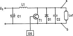
Fig. 2 represents the concise and to the point diagrammatic sketch for the preferred circuit device of the lamp that uses relatively little required maximum impulse voltage.Because lamp is in parallel with semiconductor switch in this circuit arrangement, so producible maximum impulse voltage is subjected to the restriction of the maximum blocking voltage of semiconductor switch.
Consisting of of this circuit arrangement: a buffer condenser C1, it is by a direct voltage+Uo, and for example the output voltage of a rectification circuit or a battery is powered and is worked as the feedback accumulator; A series loop of forming by tanke circuit inductance L1 and bipolar transistor T1 and sustained diode 1, this series loop is connected on the negative conductor of buffer capacitor C1; And a tank capacitor C2, it is in parallel with transistor T 1.The lamp La1 of an electrode with dielectric isolation is by terminal a, and b and tank capacitor C2 are in parallel.
Transistor T 1 is by an asymmetric square-wave oscillator OS, and for example a known pulse generator IC own controls.As long as transistor T 1 conducting is flow through the linear electric current that rises by it and by tanke circuit inductance L1.Terminal point electric current at ON time t1 reaches peak I s.In the magnetic of on tanke circuit inductance L1, storing on this time point be:
Wm=0.5·L
1·I
s 2 (1)
When time point t=t1, transistor T 1 is turned off and the following free oscillation of one-period then takes place:
In the case, magnetic energy Wm makes oscillating capacitance C2 be charged to voltage U
C2, this voltage is provided by energy Wm according to following formula:
Wm=0.5L1Is
2=0.5C2U
C2 2(3) promptly,
To series connection oscillating circuit C1, L1, C2 calculating the time, the capacitance of buffer condenser C1 is typically a few μ F, and the capacitance that it is typically the oscillating capacitor C2 of some 100pF relatively can be left in the basket.
Has amplitude V
C2The pure oscillation positive half wave of tank capacitor C2 supply with transistor T 1 in parallel and block inverse parallel diode D1.Its negative half-wave is by diode D1 clamp, and tanke circuit inductance L1 stores energy on the feedback storage capacitor C1.Produce in this way and have the seemingly half-sinusoid pulse voltage Ui of its amplitude much larger than supply power voltage Uo.In the case, voltage pulse width is:
Circuit modification in Fig. 3 presentation graphs 2, it is equally applicable to use the lamp of higher maximum impulse voltage.Wherein same element uses identical label.Here replaced the tanke circuit inductance L1 among Fig. 2 with a transformer TR1.Lamp La1 is by terminal a ', and b ' is connected on the secondary winding TR1-B of transformer TR1.Can make lamp with a maximum impulse voltage power supply thus, this pulse voltage obviously is higher than the maximum blocking voltage of semiconductor switch T1.
As under the circuit conditions of Fig. 2, transistor T 1 is by an asymmetric square-wave oscillator OS control.In transistor T 1 conducting state, the linear electric current that rises will flow through inductance value be LP transformer TR1 elementary winding TR1-A and flow through transistor T 1.This electric current reaches its peak I S when ON time t1 finishes.On the point, the energy storage of primary inductance Lp is at this moment:
Wm=0.5·Lp·Is
2 (6)
When time point t=t1, transistor T 1 is turned off, and the following free oscillation of one-period then takes place:
In the case, tank circuit inductance C2 is charged to voltage U by magnetic energy Wm
C2, this voltage is following corresponding to magnetic energy Wm:
Wm=0.5·Lp·Is
2=0.5·C2·U
C2 2 (8)
That is,
Therefore on the elementary winding of transformer TR1, produce voltage:
U
LP=U
C2-Uo (10)
This voltage U p will be according to the no-load voltage ratio of transformer TR1:
Transform on the secondary winding TR1-B, and then to the lamp La1 power supply that is connected the there.In equation (11), Ws represents that the secondary winding number of turns and Wp represent the elementary winding number of turns.Therefore the voltage on the transformer TR1 secondary winding TR1-B is:
U
LS=U
CP·ü。(12)
Has amplitude U
C2The pure oscillation positive half wave of oscillating capacitor C2 supply with transistor T 1 in parallel and block inverse parallel diode D1.Its negative half-wave is by diode D1 clamp, and energy is stored on the feedback energy storage capacitor C1 by feedback by transformer TR1 primary inductance Lp.
During the feedback energy storage, the voltage on the primary inductance Lp is:
U
LP=Uo (13)
It is switched on the secondary winding TR1-B according to the no-load voltage ratio ü of transformer TR1 equally.Therefore promptly on the time, be added with bias voltage on the lamp La1 during the pulse emission pause in the dead zone.In order to get rid of the adverse effect to lamp work, this circuit designs in this wise, promptly makes this bias voltage much smaller than pulse voltage.
A favourable modification summarily having represented Fig. 3 circuit in Fig. 4, it is equally applicable to the lamp that uses higher maximum impulse voltage.
In this modification, transformer TR1 is replaced by autotransformer TR2, and its elementary winding TR2-A is as perceptual energy accumulator, and its secondary winding TR2-B is connected the respective terminal a of tank capacitor C2 and lamp La1 " between.Therefore lamp La1 is by terminal a ", b " is connected on the series circuit of secondary winding TR2-B and tank capacitor C2 in parallel.Be that the scheme of Fig. 3 has favourable turn ratio relatively by the advantage that this scheme produced.For example for the voltage that makes the elementary relatively winding TR2-A of voltage between the lamp lead is three times and since elementary winding TR2-A secondary winding TR2-B have identical around to and be electrically connected, therefore as long as two times no-load voltage ratio is just much of that.And this is needed three times no-load voltage ratio for the scheme of Fig. 3.Can see described function when other function of flexible program is corresponding to key-drawing 3 just now among Fig. 4 thus.The other advantage of scheme is less leakage inductance among Fig. 3 relatively, less consumption and less winding electric capacity.Because less winding electric capacity can make potential pulse have steeper pulse edge, this effective work for the lamp of giving out light of the dielectric isolation discharge of using pulsed drive is favourable.
In Fig. 5, express the electric current (CH2) of elementary winding TR2-A of the control signal (CH1) that is used for transistor T 1 and the voltage (CH3) on the lamp La1.Be target time t (unit is equivalent to 2 μ S) on X-axis, reaching in Y-axis is with arbitrary unit target respective strengths.As can be seen from Figure 5, the time out between two potential pulses is controlled the influence of signal period T length.Its requirement as seen from Figure 5 similarly: on the one hand, the turn-off time t2 of transistor T 1 must be greater than the width t1 of potential pulse because otherwise the trailing edge of potential pulse can be cut off; On the other hand, turn-off time t2 must finish before the current over-zero among the tanke circuit inductance L1, because otherwise can be by interference oscillatory occurring.ON time width t1 by transistor T 1 can influence the time-out duration between each potential pulse.In addition, can make the electroluminescent lamp source dim light of connection by ON time t1 and these parameters of turn-off time t2.
In Fig. 6, summarily represented a modification of autotransformer circuit among Fig. 4.Here tank capacitor is by lamp La1 natural capacity (not shown) or the lamp electric capacity by the autotransformer conversion and additionally realize by MOSFET T2 barrier layer electric capacity (not shown).Here can abandon using additional tank circuit inductance as discrete capacitor form among Fig. 4.Can abandon using discrete fly-wheel diode in addition, because its function is replaced by the parasitic diode (not shown) among the MOSFET T2.Remaining circuit part and operation principle are corresponding among Fig. 4 those.Therefore, lamp La1 is by means of terminal a , and the series circuit of b and secondary winding TR2-B and MOSFET T2 is in parallel.This circuit modifications is with using described less element to realize.
Claims (13)
1. illuminator has
A pulse voltage source, it is suitable for providing at work the potential pulse of being separated by time out,
The discharge lamp of a dielectric isolation (La1) has
One is partially transparent at least and that be filled with air seal or can be flow through and open discharge vessel by gas or admixture of gas, and it is made by electrically non-conductive material, and
Electrode, it is connected with pulse voltage source, and wherein the electrode of at least one polarity separates by dielectric material and discharge vessel inside,
And wherein, this pulse voltage source has a circuit arrangement that is used to produce pulse voltage series, and these pulse voltage series are used to operate the interior dielectric isolation discharge of discharge vessel of the discharge lamp (La1) of dielectric isolation,
Described illuminator has
A tanke circuit inductance (L1; TR1-A, TR2-A),
A gate-controlled switch (T1, T2), it and tanke circuit inductance (L1; TR1-A; TR2-A) series connection,
A pulse generator (OS), its control switch (T1),
A current valve (D1), it and switch (T1) inverse parallel, wherein, this current valve is by a hidden element or plays integrated source-leakages diode formation of the MOSFET (T2) of on-off action,
A tank circuit inductance (C2), it is in parallel with switch (T1), wherein, tank circuit inductance be by a hidden element or partly the natural capacity of the discharge lamp (La1) of the barrier layer electric capacity by a MOSFET (T2) who plays on-off action and/or this dielectric isolation of joining form
Device (a, a b who is used to connect the discharge lamp (La1) of this dielectric isolation; TR1-B, a ' b '; TR2-B, a ", b "),
Wherein, control signal by pulse generator (OS) when work alternately makes switch (T1, T2) conducting or blocking-up produce the sequence of voltage pulses that is suspended time-division thus between the electrode of the discharge lamp (La1) of a dielectric isolation that is connected with this device.
2. according to the illuminator of claim 1, it is characterized in that: in the scope of the value of tank circuit inductance between 100pF and 1 μ F.
3. according to the illuminator of claim 1, it is characterized in that: in the scope of the value of tanke circuit inductance between 500 μ H and 10mH.
4. according to the illuminator of claim 1, it is characterized in that: gate-controlled switch is a controllable semiconductor device.
5. according to the illuminator of claim 4, it is characterized in that: described controllable semiconductor device is a transistor (T1; T2).
6. according to the illuminator of claim 4, it is characterized in that: this controllable semiconductor device be a metal oxide semiconductor field effect tube (MOSFET) (T2).
7. according to the illuminator of claim 1, it is characterized in that: this current valve is a diode (D1).
8. according to the illuminator of one of claim 1-7, it is characterized in that: the device that is used to connect the discharge lamp (La1) of this dielectric isolation comprises that (a, b), they respectively are connected with a utmost point of a switch (T1) two terminals.
9. illuminator according to Claim 8, it is characterized in that: the device that is used to connect the discharge lamp (La1) of this dielectric isolation additionally comprises the secondary winding (TR2-B) of an autotransformer (TR2), this secondary winding (TR2-B) be connected switch (T1, the respective terminal of first utmost point T2) and electric discharge device (La1) (a "; A ) between, the wherein effect of elementary winding (TR2-A) the oscillates loop inductance of autotransformer (TR2).
10. according to the illuminator of one of claim 1 to 7, it is characterized in that: the device that is used to connect this dielectric isolation discharge lamp (La1) comprise the secondary winding (TR1-B) of a transformer (TR1) and two terminals (a ', b '), each terminal is connected with a utmost point of secondary winding (TR1-B), wherein the effect of elementary winding (TR1-A) the oscillates loop inductance of transformer (TR1).
11. the illuminator according to claim 1 is characterized in that: at tanke circuit inductance (L1; TR1-A; TR2-A) buffering additionally in parallel and feedback energy storage capacitor (C1) and on the series circuit of switch (T1).
12. the illuminator according to claim 11 is characterized in that: the capacitance of buffering and feedback energy storage capacitor (C1) is greater than the value of tank circuit inductance (C2).
13. the illuminator according to claim 1 is characterized in that: pulse generator is a square-wave generator integrated circuit (IC).
Applications Claiming Priority (2)
| Application Number | Priority Date | Filing Date | Title |
|---|---|---|---|
| DE19731275.6 | 1997-07-22 | ||
| DE19731275 | 1997-07-22 |
Publications (2)
| Publication Number | Publication Date |
|---|---|
| CN1234958A CN1234958A (en) | 1999-11-10 |
| CN1183807C true CN1183807C (en) | 2005-01-05 |
Family
ID=7836406
Family Applications (1)
| Application Number | Title | Priority Date | Filing Date |
|---|---|---|---|
| CNB988010321A Expired - Lifetime CN1183807C (en) | 1997-07-22 | 1998-06-24 | Process for producing voltage pulse sequences and circuit assembly therefor |
Country Status (12)
| Country | Link |
|---|---|
| US (1) | US6323600B1 (en) |
| EP (1) | EP0927506B1 (en) |
| JP (1) | JP2001502843A (en) |
| KR (1) | KR100467875B1 (en) |
| CN (1) | CN1183807C (en) |
| AT (1) | ATE208121T1 (en) |
| CA (1) | CA2267366C (en) |
| DE (1) | DE59801941D1 (en) |
| ES (1) | ES2167927T3 (en) |
| HK (1) | HK1023684A1 (en) |
| TW (1) | TW457773B (en) |
| WO (1) | WO1999005892A1 (en) |
Families Citing this family (32)
| Publication number | Priority date | Publication date | Assignee | Title |
|---|---|---|---|---|
| JP3296284B2 (en) * | 1998-03-12 | 2002-06-24 | ウシオ電機株式会社 | Dielectric barrier discharge lamp light source device and its power supply device |
| DE10005975A1 (en) | 2000-02-09 | 2001-08-16 | Patent Treuhand Ges Fuer Elektrische Gluehlampen Mbh | Operating method for a discharge lamp with at least one dielectric barrier electrode |
| DE10111191A1 (en) | 2001-03-08 | 2002-09-19 | Patent Treuhand Ges Fuer Elektrische Gluehlampen Mbh | Electrical contact system e.g. for flat radiator of LCD system, has receptacle for insulating body with mounted contact part |
| DE10133326A1 (en) | 2001-07-10 | 2003-01-23 | Patent Treuhand Ges Fuer Elektrische Gluehlampen Mbh | Dielectric barrier discharge lamp with ignition aid |
| DE10145993A1 (en) * | 2001-09-18 | 2003-04-24 | Siemens Ag | High voltage pulse generator for an electrostatic filter |
| DE10147961A1 (en) * | 2001-09-28 | 2003-04-10 | Patent Treuhand Ges Fuer Elektrische Gluehlampen Mbh | Igniting, operating dielectric barrier discharge lamp involves applying ignition voltage between sub-electrodes to ignite auxiliary discharge at gap between sub-electrodes during ignition |
| TWI268035B (en) * | 2003-01-10 | 2006-12-01 | Sunyen Co Ltd | Energy storage circuitry system |
| DE10333729A1 (en) * | 2003-07-23 | 2005-03-10 | Patent Treuhand Ges Fuer Elektrische Gluehlampen Mbh | Ballast for at least one high-pressure discharge lamp, operating method and lighting system for a high-pressure discharge lamp |
| DE10359882A1 (en) * | 2003-12-19 | 2005-07-14 | Patent-Treuhand-Gesellschaft für elektrische Glühlampen mbH | Circuit arrangement for operating electric lamps |
| JP2007518387A (en) | 2004-01-09 | 2007-07-05 | コーニンクレッカ フィリップス エレクトロニクス エヌ ヴィ | High-efficiency single-ended forward flyback electronic driver for barrier discharge lamps |
| DE102004020398A1 (en) * | 2004-04-23 | 2005-11-10 | Patent-Treuhand-Gesellschaft für elektrische Glühlampen mbH | Dielectric barrier discharge lamp with external electrodes and lighting system with this lamp |
| US8110998B2 (en) | 2004-07-21 | 2012-02-07 | Koninklijke Philips Electronics N.V. | Multi-pulse ignition circuit for a gas discharge lamp |
| DE102004047372A1 (en) * | 2004-09-29 | 2006-03-30 | Patent-Treuhand-Gesellschaft für elektrische Glühlampen mbH | Converter circuit with class E converter modules |
| CN100364486C (en) * | 2004-11-01 | 2008-01-30 | 蒋中为 | Strong pulsation light generator for medical beautifying |
| TWI285519B (en) * | 2005-11-04 | 2007-08-11 | Delta Electronics Inc | Method adopting square voltage waveform for driving flat lamps |
| DE102005034505A1 (en) | 2005-07-20 | 2007-02-01 | Patent-Treuhand-Gesellschaft für elektrische Glühlampen mbH | Circuit arrangement with transformerless converter with choke for the pulsed operation of dielectric barrier discharge lamps |
| DE102005037352A1 (en) * | 2005-08-08 | 2007-02-15 | Patent-Treuhand-Gesellschaft für elektrische Glühlampen mbH | Circuit arrangement and method for operating at least one dielectrically impeded discharge lamp |
| US7221100B2 (en) * | 2005-08-12 | 2007-05-22 | Alameda Applied Sciences Corp. | Gas discharge lamp power supply |
| FR2891775B1 (en) * | 2005-10-07 | 2008-02-01 | Alstom Transport Sa | METHOD AND SYSTEM FOR POWERING AN POWER BUS OF AN ELECTRIC VEHICLE, RECORDING MEDIUM, AND VEHICLE FOR THE METHOD |
| TW200721907A (en) * | 2005-11-18 | 2007-06-01 | Delta Optoelectronics Inc | An improved startup method for the mercury-free flat-fluorescent lamp |
| DE202006005212U1 (en) * | 2006-03-31 | 2006-07-20 | Patent-Treuhand-Gesellschaft für elektrische Glühlampen mbH | Lighting system with dielectric barrier discharge lamp has flat strip two wire high voltage cable connecting high voltage generator to lamp electrodes |
| TW200740300A (en) * | 2006-04-04 | 2007-10-16 | Delta Optoelectronics Inc | Driving circuit and method for fluorescent lamp |
| DE202007004236U1 (en) * | 2007-03-22 | 2007-06-14 | Patent-Treuhand-Gesellschaft für elektrische Glühlampen mbH | Dielectric barrier discharge lamp with ignition aid |
| US7446488B1 (en) | 2007-08-29 | 2008-11-04 | Osram Sylvania | Metal halide lamp ballast controlled by remote enable switched bias supply |
| GB0805785D0 (en) * | 2008-03-31 | 2008-04-30 | Cyden Ltd | Control circuit for flash lamps or the like |
| FR2940741A1 (en) * | 2008-12-31 | 2010-07-02 | Saint Gobain | Impulsional electrical power circuit i.e. pulse ballast, for supplying power to planar discharge lamp of lighting system in e.g. shop, has current source connected to common point of primary and third self-inductors of branch of lamp |
| DE102009019904A1 (en) * | 2009-05-04 | 2010-11-25 | Osram Gesellschaft mit beschränkter Haftung | Circuit arrangement and method for operating discharge lamps |
| EP2524580A2 (en) * | 2010-09-22 | 2012-11-21 | Osram AG | Method for starting a high-pressure discharge lamp |
| CN102176643B (en) * | 2011-03-09 | 2013-08-28 | 福州大学 | Single-stage three-phase current type inverter with large step-up ratio |
| DE102016213944A1 (en) * | 2016-07-28 | 2018-02-01 | Ellenberger & Poensgen Gmbh | Method and device for driving a semiconductor switch |
| WO2021035616A1 (en) * | 2019-08-29 | 2021-03-04 | 深圳市大疆创新科技有限公司 | Drive circuit, drive circuit board and driver |
| CN111239507A (en) * | 2019-11-05 | 2020-06-05 | 南方电网科学研究院有限责任公司 | Oil paper insulation surface charge measuring device and measuring method thereof |
Family Cites Families (18)
| Publication number | Priority date | Publication date | Assignee | Title |
|---|---|---|---|---|
| US5446346A (en) * | 1978-03-20 | 1995-08-29 | Nilssen; Ole K. | Electronic ballast with controlled DC supply voltage |
| JPS6070698A (en) * | 1983-09-27 | 1985-04-22 | Toshiba Corp | Device for heating filament of x-ray tube |
| US4720668A (en) * | 1986-06-20 | 1988-01-19 | Lee Fred C | Zero-voltage switching quasi-resonant converters |
| US4742278B1 (en) * | 1987-06-03 | 1996-11-05 | Bertonee Inc | Single connection gas discharge display and driver |
| AU607520B2 (en) | 1987-08-06 | 1991-03-07 | Shing Cheung Chow | Discharge lamp type display device |
| US5065072A (en) * | 1989-03-31 | 1991-11-12 | Valeo Vision | Power supply circuit for an arc lamp, in particular for a motor vehicle headlight |
| US5041767A (en) | 1990-03-30 | 1991-08-20 | Bertonee Inc. | Digital controller for gas discharge tube |
| DE9015674U1 (en) * | 1990-11-15 | 1992-03-12 | Patent-Treuhand-Gesellschaft Fuer Elektrische Gluehlampen Mbh, 8000 Muenchen, De | |
| US5144204A (en) * | 1991-05-28 | 1992-09-01 | General Electric Company | Tapped-inductor boost convertor for operating a gas discharge lamp |
| NO913368D0 (en) * | 1991-08-27 | 1991-08-27 | Julius Hartai | FREQUENCY MODULATED DRIVER WITH PARALLEL RESONANCE. |
| US5982645A (en) * | 1992-08-25 | 1999-11-09 | Square D Company | Power conversion and distribution system |
| DE4311197A1 (en) * | 1993-04-05 | 1994-10-06 | Patent Treuhand Ges Fuer Elektrische Gluehlampen Mbh | Method for operating an incoherently radiating light source |
| US5623187A (en) * | 1994-12-28 | 1997-04-22 | Philips Electronics North America Corporation | Controller for a gas discharge lamp with variable inverter frequency and with lamp power and bus voltage control |
| US5798616A (en) * | 1995-04-06 | 1998-08-25 | Minebea Co., Ltd. | Fluorescent lamp circuit employing both a step-up chopper and an inverter |
| DE19548003A1 (en) | 1995-12-21 | 1997-06-26 | Patent Treuhand Ges Fuer Elektrische Gluehlampen Mbh | Circuit arrangement for generating pulse voltage sequences, in particular for the operation of dielectrically impeded discharges |
| JP3277788B2 (en) * | 1996-01-16 | 2002-04-22 | ウシオ電機株式会社 | Discharge lamp lighting device |
| US5684683A (en) * | 1996-02-09 | 1997-11-04 | Wisconsin Alumni Research Foundation | DC-to-DC power conversion with high current output |
| DE19712258A1 (en) * | 1997-03-24 | 1998-10-01 | Patent Treuhand Ges Fuer Elektrische Gluehlampen Mbh | Circuit for igniting a high-pressure discharge lamp |
-
1998
- 1998-06-24 DE DE59801941T patent/DE59801941D1/en not_active Expired - Lifetime
- 1998-06-24 JP JP11509158A patent/JP2001502843A/en active Pending
- 1998-06-24 EP EP98942458A patent/EP0927506B1/en not_active Expired - Lifetime
- 1998-06-24 AT AT98942458T patent/ATE208121T1/en not_active IP Right Cessation
- 1998-06-24 ES ES98942458T patent/ES2167927T3/en not_active Expired - Lifetime
- 1998-06-24 KR KR10-1999-7002429A patent/KR100467875B1/en not_active IP Right Cessation
- 1998-06-24 US US09/254,938 patent/US6323600B1/en not_active Expired - Lifetime
- 1998-06-24 CN CNB988010321A patent/CN1183807C/en not_active Expired - Lifetime
- 1998-06-24 CA CA002267366A patent/CA2267366C/en not_active Expired - Lifetime
- 1998-06-24 WO PCT/DE1998/001723 patent/WO1999005892A1/en active IP Right Grant
- 1998-07-15 TW TW087111523A patent/TW457773B/en not_active IP Right Cessation
-
2000
- 2000-05-10 HK HK00102814A patent/HK1023684A1/en not_active IP Right Cessation
Also Published As
| Publication number | Publication date |
|---|---|
| EP0927506B1 (en) | 2001-10-31 |
| DE59801941D1 (en) | 2001-12-06 |
| WO1999005892A1 (en) | 1999-02-04 |
| EP0927506A1 (en) | 1999-07-07 |
| US6323600B1 (en) | 2001-11-27 |
| CN1234958A (en) | 1999-11-10 |
| HK1023684A1 (en) | 2000-09-15 |
| KR100467875B1 (en) | 2005-01-24 |
| CA2267366A1 (en) | 1999-02-04 |
| JP2001502843A (en) | 2001-02-27 |
| ATE208121T1 (en) | 2001-11-15 |
| TW457773B (en) | 2001-10-01 |
| CA2267366C (en) | 2006-01-10 |
| KR20000068607A (en) | 2000-11-25 |
| ES2167927T3 (en) | 2002-05-16 |
Similar Documents
| Publication | Publication Date | Title |
|---|---|---|
| CN1183807C (en) | Process for producing voltage pulse sequences and circuit assembly therefor | |
| CN1101618C (en) | Pulse voltage series circuit for producing electric medium block discharge | |
| CN1074605C (en) | Contravariant device | |
| CN1120565C (en) | Method and circuit for resonance inversion | |
| CN1930924A (en) | Hybrid power supply system | |
| CN210518900U (en) | High-power microwave power supply with adjustable duty ratio | |
| CN1270128C (en) | Microwave oven and its control method | |
| CN1533225A (en) | Discharging lamp ignitor | |
| JP2002525810A (en) | Electronic Pre-Circuit Device for Discharge Lamp with Dielectric Disturbance Discharge | |
| EP1441566A3 (en) | Variable-frequency inverter microwave oven and method for controlling the same | |
| US7151344B2 (en) | Electroluminescent driver circuit | |
| CN1781134A (en) | Energy recovery device for a plasma display panel | |
| JP4502659B2 (en) | Pulse generator | |
| CN1122491A (en) | Lamp starting apparatus for liquid crystal projector | |
| CN1902987A (en) | High-efficiency single-ended forward-flyback electronic driver for barrier discharge lamps | |
| CN1960592A (en) | Plasma lighting system and driving control method thereof | |
| CN101061757A (en) | Electric-discharge lamp operation device | |
| CN212441926U (en) | Piezoelectric shock wave driving device and piezoelectric shock wave equipment | |
| CN2185010Y (en) | Silicon control high frequency high voltage dc power source | |
| US6624595B2 (en) | Resonant energy recovery for electro-luminescent lamp panels | |
| RU2307462C1 (en) | Device for powering impulse lamps | |
| RU55233U1 (en) | PULSE LAMP POWER SYSTEM (OPTIONS) | |
| CN2796292Y (en) | Electronic neon lmp transformer for preventing mercury displacement | |
| CN201830203U (en) | Piezoelectric device drive circuit module based on frequency doubling resonant switch technology | |
| CN115118153A (en) | H-bridge driving circuit, driving method and device based on charge pump |
Legal Events
| Date | Code | Title | Description |
|---|---|---|---|
| C06 | Publication | ||
| PB01 | Publication | ||
| C10 | Entry into substantive examination | ||
| SE01 | Entry into force of request for substantive examination | ||
| C14 | Grant of patent or utility model | ||
| GR01 | Patent grant | ||
| CX01 | Expiry of patent term | ||
| CX01 | Expiry of patent term |
Granted publication date: 20050105 |