JP4502659B2 - Pulse generator - Google Patents
Pulse generator Download PDFInfo
- Publication number
- JP4502659B2 JP4502659B2 JP2004044628A JP2004044628A JP4502659B2 JP 4502659 B2 JP4502659 B2 JP 4502659B2 JP 2004044628 A JP2004044628 A JP 2004044628A JP 2004044628 A JP2004044628 A JP 2004044628A JP 4502659 B2 JP4502659 B2 JP 4502659B2
- Authority
- JP
- Japan
- Prior art keywords
- diode
- capacitor
- inductive load
- voltage
- cathode
- Prior art date
- Legal status (The legal status is an assumption and is not a legal conclusion. Google has not performed a legal analysis and makes no representation as to the accuracy of the status listed.)
- Expired - Fee Related
Links
- 239000003990 capacitor Substances 0.000 claims description 61
- 230000001939 inductive effect Effects 0.000 claims description 59
- 239000004065 semiconductor Substances 0.000 claims description 31
- 238000007599 discharging Methods 0.000 claims description 12
- 238000010586 diagram Methods 0.000 description 7
- 230000006698 induction Effects 0.000 description 3
- 238000011069 regeneration method Methods 0.000 description 3
- 238000010438 heat treatment Methods 0.000 description 2
- 238000005259 measurement Methods 0.000 description 2
- 238000000034 method Methods 0.000 description 2
- 230000008929 regeneration Effects 0.000 description 2
- 240000007320 Pinus strobus Species 0.000 description 1
- 238000005452 bending Methods 0.000 description 1
- 238000007796 conventional method Methods 0.000 description 1
- 238000011161 development Methods 0.000 description 1
- 230000018109 developmental process Effects 0.000 description 1
- 238000005265 energy consumption Methods 0.000 description 1
- 238000002474 experimental method Methods 0.000 description 1
- 229910052736 halogen Inorganic materials 0.000 description 1
- 150000002367 halogens Chemical class 0.000 description 1
- 230000020169 heat generation Effects 0.000 description 1
- 238000012545 processing Methods 0.000 description 1
- 230000001172 regenerating effect Effects 0.000 description 1
- 230000003252 repetitive effect Effects 0.000 description 1
- 230000000630 rising effect Effects 0.000 description 1
- 238000004804 winding Methods 0.000 description 1
Images


Landscapes
- Rectifiers (AREA)
- Generation Of Surge Voltage And Current (AREA)
Description
本発明はパルス発生装置に関し、特に、従来のマルクス回路に似たコンデンサ充放電回路を用い、誘導性負荷に残留している磁気エネルギーを、電荷の形で静電エネルギーとして各コンデンサに充電し、次回の誘導性負荷へのパルスの印加時に、各コンデンサの電荷を放電することを可能としたパルス発生装置に関する。 The present invention relates to a pulse generator, and in particular, using a capacitor charge / discharge circuit similar to a conventional Marx circuit , the magnetic energy remaining in the inductive load is charged to each capacitor as electrostatic energy in the form of electric charge, The present invention relates to a pulse generator capable of discharging the charge of each capacitor when a pulse is next applied to an inductive load.
マルクス回路は、衝撃電圧発生回路とも呼ばれ、従来のパルス発生装置に利用されていた。図1は、従来の手法で構成したマルクス型回路10(4段構成)を利用したパルス発生装置の一例を示す図である。図1に基づいてその動作を説明する。
図1において、r 1 乃至r 8 は充電抵抗、C 1 乃至C 4 は充電用の各コンデンサ、GS 1乃至GS 5はギャップスイッチである。まず、充電サイクルにおいては、電源6から供給されたエネルギーは、点線の矢印で示す(1)の経路で、各コンデンサ(C 1 乃至C 4 )を充電する。各コンデンサ(C 1 乃至C 4 )が充電されると、放電サイクルにおいて、各ギャップスイッチ(GS 1 乃至GS 5 )をON(火花放電)させ、各コンデンサ(C 1 乃至C 4 )を、(2)の経路で直列に接続して放電させることにより、負荷(図1では誘導性負荷5)に各コンデンサ(C 1 乃至C 4 )の充電電圧(ほぼ電源6の電圧に等しい)の段数倍にあたるパルスを印加するようになっている(特許文献1参照)。
In FIG. 1, r 1 to r 8 are charging resistors, C 1 to C 4 are charging capacitors, and G S 1 to G S 5 are gap switches. First, in the charging cycle, the energy supplied from the
しかしながら、負荷において、高電圧のパルスが必要なのは一瞬であるにもかかわらず、ギャップスイッチには遮断(カットOFF)機能がないため、各コンデンサに充電されたエネルギーは、毎回放電時になくなるまで無駄な電流が流れ、負荷において熱として消費されてしまうという欠点があった。そのため、各コンデンサを再充電するのに時間とエネルギーが必要であり、高い繰り返しで、各コンデンサを充電・放電を行うことはできなかった。 However, the gap switch does not have a cutoff (cut-off) function in spite of the moment that a high voltage pulse is required in the load. There is a drawback that current flows and is consumed as heat in the load. For this reason, it takes time and energy to recharge each capacitor, and it was impossible to charge and discharge each capacitor with high repetition.
一方、医療用小型加速器の開発が、我が国で国家プロジェクトとして推進されている。医療用小型加速器の型式はさまざまであるが、医療用小型加速器の偏向電磁石に、数10kJの磁気エネルギーパルス放電を、最大毎秒10回程度行うことが求められている。また、これに用いられるパルス電源は、消費電力が少なく、偏向電磁石のコイルの発熱を最小限にでき、かつ、入力電力も安定化したものである必要がある。
各コンデンサを並列に接続して充電・直列に接続して放電というマルクス回路の特徴を活かしつつ、上述の欠点を克服した新しいタイプのパルス発生装置が求められている。
本発明は上述の課題に応えるために為されたものであり、本発明は、誘導性負荷に高い繰り返しでパルスを供給する、マルクス型回路を利用したパルス発生装置を提供することを目的とする。
On the other hand, development of a small medical accelerator is being promoted as a national project in Japan. Type type medical small type accelerator is a variety, the bending magnet of the medical small type accelerator, a magnetic energy pulsed discharge of several 10 kJ, it is required to perform a maximum of about 10 times per second. Further, the pulse power source used for this needs to have low power consumption, minimize heat generation of the deflection electromagnet coil, and stabilize the input power.
There is a need for a new type of pulse generator that overcomes the above-mentioned drawbacks while taking advantage of the Marx circuit's characteristics of charging and connecting in series by connecting capacitors in parallel and discharging in series.
The present invention has been made to meet the above-mentioned problems, the present invention provides a pulse at a high repetition the inductive load, and an object thereof is to provide a pulse generator utilizing a Marx-type circuit .
本発明は、パルス発生装置に関し、本発明の上記目的は、電源と誘導性負荷との間に直列に接続され、前記誘導性負荷に繰り返しパルスを供給するパルス発生装置であって、該パルス発生装置は、コンデンサ充放電回路と制御手段とを備えるとともに、前記コンデンサ充放電回路は、第1のダイオードのカソードと第2のダイオードのアノードとの間にコンデンサを接続し、前記第1のダイオードのカソードと前記第2のダイオードのカソードとの間に前記第1のダイオードのカソード側を正極として半導体スイッチを接続して成る単位回路ユニットをN(2≦N)段直列に接続し、さらに、第1段目の前記単位回路ユニットの第1のダイオードのアノードと第2のダイオードのアノードとの間に、前記第1のダイオードのアノード側を正極としてさらに半導体スイッチを接続して構成されたものであって、
前記コンデンサ充放電回路を構成する前記各単位回路ユニットは、互いに、第k段目(1≦k≦N−1)の第1のダイオードのカソードと第(k+1)段目の第1のダイオードのアノードとが接続され、前記第k段目の第2のダイオードのカソードと前記第(k+1)段目の第2のダイオードのアノードとが接続されており、前記第1段目の単位回路ユニットの第1のダイオードのアノードが前記電源に接続され、さらに、前記第N段目の単位回路ユニット第2のダイオードのカソードが前記誘導性負荷に接続されるとともに、
前記制御手段は、
すべての前記半導体スイッチを、所定のタイミングで同時にONにして前記コンデンサ充放電回路の前記各コンデンサを直列に接続し、前記誘導性負荷に、前記電源電圧と前記各コンデンサの充電電圧との総和に相当する前記パルスの電圧を供給し、さらに、所定のタイミングで同時にOFFにして、前記誘導性負荷に残留している磁気エネルギーを、電荷の持つ静電エネルギーの形で前記各コンデンサに回生し、前記各コンデンサへの充電を行うように制御することを特徴とするパルス発生装置によって達成される。
The present invention relates to a pulse generator, the object of the present invention are connected in series between the power supply and the inductive load, a pulse generator for supplying a repetitive pulses to the inductive load, the pulse generator The apparatus includes a capacitor charging / discharging circuit and control means, and the capacitor charging / discharging circuit connects a capacitor between the cathode of the first diode and the anode of the second diode, and A unit circuit unit formed by connecting a semiconductor switch between the cathode and the cathode of the second diode with the cathode side of the first diode as a positive electrode is connected in series (2 ≦ N) stages, and The anode side of the first diode is positively connected between the anode of the first diode and the anode of the second diode of the unit circuit unit in the first stage. Be one that is configured by further connecting the semiconductor switches and,
The unit circuit units constituting the capacitor charging / discharging circuit are connected to each other of the cathode of the first diode of the k-th stage (1 ≦ k ≦ N−1) and the first diode of the (k + 1) -th stage. An anode is connected, and a cathode of the second diode of the k-th stage is connected to an anode of the second diode of the (k + 1) -th stage, and the unit circuit unit of the first stage is connected The anode of the first diode is connected to the power supply, and the cathode of the second stage unit circuit unit second diode is connected to the inductive load.
The control means includes
The total sum of all of the semiconductor switches, and the ON time at a predetermined timing to connect the respective capacitor of the capacitor charge and discharge circuit in series, the inductive load, the power source voltage and the charging voltage of each capacitor supplying a voltage of the pulses corresponding to, further, in the OFF simultaneously at a predetermined timing, the magnetic energy remaining in the inductive load, the regenerated into each capacitor in the form of electrostatic energy of the charge It is achieved by a pulse generator and controls to perform the charging of the respective capacitors.
本発明に係るパルス発生装置によれば、誘導性負荷に供給する電流を任意のタイミングで遮断し、誘導性負荷に残留している磁気エネルギーを、電荷の持つ静電エネルギーの形で各コンデンサに回生することができるので、再び各コンデンサを充電するエネルギーが少なくてすみ、高い繰り返しでパルスを効率よく発生させることができる。
また、各コンデンサの電圧は、主として誘導性負荷に残留している磁気エネルギーを、電荷の持つ静電エネルギーの形で回生することにより作られるので、電源電圧は、各コンデンサの充電電圧よりも低くてもよい特徴がある。これは、誘導性負荷の抵抗分の電圧があれば、その電流が流れるようになるまで、各コンデンサ電圧が上昇するからである。
According to the pulse generator of the present invention, the current supplied to the inductive load is interrupted at an arbitrary timing, and the magnetic energy remaining in the inductive load is transferred to each capacitor in the form of electrostatic energy possessed by charges. Since regeneration is possible, less energy is required to charge each capacitor again, and pulses can be generated efficiently with high repetition.
In addition, the voltage of each capacitor is generated mainly by regenerating the magnetic energy remaining in the inductive load in the form of electrostatic energy possessed by electric charges, so the power supply voltage is lower than the charging voltage of each capacitor. There are features that may be. This is because if there is a voltage corresponding to the resistance of the inductive load, each capacitor voltage rises until the current flows.
本発明に係るパルス発生装置の特徴は、誘導性負荷に残留している磁気エネルギーを有効に利用して、高電圧の電源を用意せずに高電圧のパルスを瞬時に得るという点である。誘導性負荷のインダクタに蓄えられた磁気エネルギーを利用することで、高速に各コンデンサを充電することができ、高い繰り返しでパルスを発生させることが可能になる。 Features of the pulse generator according to the present invention, by effectively utilizing the magnetic energy remaining in the inductive load, in terms of obtaining instant is a pulse of high voltage without providing a power supply of high voltage . By using the magnetic energy stored in the inductor of the inductive load, each capacitor can be charged at high speed, and pulses can be generated with high repetition.
図2は、本発明に係るパルス発生装置の構成の実施例(4段の場合)を示す図である。より詳しくは、パルス発生装置は、コンデンサ充放電回路(図1の従来のマルクス型回路10の充電抵抗rをダイオードで、ギャップスイッチGSを半導体スイッチSでそれぞれ置き換えた形となっている。)と、制御手段3を具備している。コンデンサ充放電回路は、図2から明らかなように、4つの単位回路ユニットを直列に接続したものと、半導体スイッチS 1 とから構成されている。より詳しくは、第k段目(1≦k≦4)の単位回路ユニットは、第1のダイオードD k1 のカソードと第2のダイオードD k2 のアノードとの間にコンデンサC k を接続し、第1のダイオードD k1 のカソードと第2のダイオードD k2 のカソードとの間に第1のダイオードD k1 のカソード側を正極として半導体スイッチS k+1 を接続して構成されるものである。
そして、コンデンサ充放電回路を構成する各単位回路ユニットは、互いに、第k段目(1≦k≦3)の第1のダイオードDk1のカソードと第(k+1)段目の第1のダイオードDk+1,1のアノードとが接続され、第k段目の第2のダイオードDk2のカソードと第(k+1)段目の第2のダイオードDk+1,2のアノードとが接続されている。
さらに、第1段目の単位回路ユニットの第1のダイオードD11のアノードと第2のダイオードD12のアノードとの間に、第1のダイオードD11のアノード側を正極として半導体スイッチS1が接続されるとともに、第1のダイオードD11のアノードが電源6に接続され、第4段目の単位回路ユニットの第2のダイオードD42のカソードが誘導性負荷5の一端に接続されている。
制御手段3は、半導体スイッチ(S1乃至S5)のON・OFF制御を行う。半導体スイッチ(S1乃至S5)がすべてONのときは、各コンデンサ(C1乃至C4)は直列に接続され放電し、半導体スイッチ(S1乃至S5)がすべてOFFになると、各コンデンサ(C1乃至C4)に、誘導性負荷5に残留している磁気エネルギーは電流となり、電荷の持つ静電エネルギーの形で回生されるとともに、電源6からの電流がダイオード(D11乃至D42)を介して流れ、各コンデンサ(C1乃至C4)が充電される。なお、図2における半導体スイッチ(S1乃至S5)は、パワーMOSFETを使用した場合を示している。
FIG. 2 is a diagram showing an embodiment (in the case of four stages) of the configuration of the pulse generator according to the present invention. More specifically, the pulse generator has a capacitor charging / discharging circuit (the charging resistor r of the conventional Marx
Each unit circuit unit constituting the capacitor charging / discharging circuit is connected to the cathode of the k-th (1 ≦ k ≦ 3) first diode D k1 and the (k + 1) -th first diode D. The anodes of k + 1 and 1 are connected, and the cathode of the k-th second diode D k2 and the anodes of the (k + 1) -th second diode D k + 1 and 2 are connected.
Furthermore, between the anode and the anode of the second diode D 12 of the first diode D 11 of the unit circuit units of the first stage, the semiconductor switch S 1 is the anode of the first diode D 11 as the positive electrode In addition, the anode of the first diode D 11 is connected to the
The control means 3 performs ON / OFF control of the semiconductor switches (S 1 to S 5 ). When the semiconductor switches (S 1 to S 5 ) are all ON, the capacitors (C 1 to C 4 ) are connected in series and discharged, and when the semiconductor switches (S 1 to S 5 ) are all OFF, the capacitors In (C 1 to C 4 ), the magnetic energy remaining in the
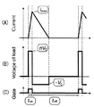
図3は、図2に示す本発明に係るパルス発生装置を構成するコンデンサ充放電回路の半導体スイッチ(S 1 乃至S 5 )のゲートの状態(図3(C))と、誘導性負荷5に流れる電流(図3(A))及び電圧VL(図3(B))の波形を示したものである。
本発明に係るパルス発生装置の動作原理を、図3に基づいて説明する。
(1)制御手段3が、半導体スイッチ(S1乃至S5)を、すべて同時にOFFにすると(図3(C)における区間toff、ゲートのOFF時間)、誘導性負荷5に残留している磁気エネルギーが電流となったもの及び電源6からの電流により、各コンデンサ(C 1 乃至C 4 )を並列に充電するため、誘導性負荷5を流れる電流は徐々に減少し始め、各コンデンサ(C 1 乃至C 4 )の充電が完了すると、誘導性負荷5に流れる電流は略ゼロになる。
また、制御手段3が、半導体スイッチ(S 1 乃至S 5 )を、すべて同時にOFFにすると、誘導性負荷5に逆起電力が生じ、誘導性負荷5に残留している磁気エネルギーは、電流となって各コンデンサ(C 1 乃至C 4 )を充電する。各コンデンサ(C 1 乃至C 4 )の充電が開始されると、誘導性負荷5の逆電圧は徐々に増え、各コンデンサ(C 1 乃至C 4 )の充電電圧(−VC)まで到達する(図3(B)における区間tchg、充電時間)。各コンデンサ(C 1 乃至C 4 )の充電が完了すると、誘導性負荷5に流れる電流は略ゼロになり、誘導性負荷5の電圧VLも略ゼロになる。
(2)次に、制御手段3が、半導体スイッチ(S 1 乃至S 5 )を、すべて同時にONにすると(図3(C)における区間tonゲートのON時間)、充電されている各コンデンサ(C 1 乃至C 4 )が直列に接続されて放電されるため(図3(B)における区間tdis、放電時間)、誘導性負荷5には、各コンデンサ(C 1 乃至C 4 )の充電電圧Vcのn段数倍の電圧(nVC)と電源6の電圧Eとの和に相当する電圧が印加される。
(3)各コンデンサ(C 1 乃至C 4 )の放電開始とともに、誘導性負荷5に流れる電流は増え(図3(A)の区間tdis)、各コンデンサ(C 1 乃至C 4 )の放電が完了すると定常状態となり、電源6の電圧Eと誘導性負荷5の抵抗Rで決まる定常電流imaxが流れるようになる。
なお、上記充電時間tchg、放電時間tdis、各コンデンサ(C 1 乃至C 4 )の充電電圧Vc及び定常電流imaxは、各コンデンサ(C 1 乃至C 4 )の静電容量C、誘導性負荷5のインダクタンスL、段数nを用いて、次の数1のように表される。

The operation principle of the pulse generator according to the present invention will be described with reference to FIG.
(1) When the control means 3 turns off all the semiconductor switches (S 1 to S 5 ) at the same time (section t off in FIG. 3C, gate OFF time), the control means 3 remains in the
When the
(2) Next, when the control means 3 turns on all the semiconductor switches ( S 1 to S 5 ) at the same time (the ON time of the section t on gate in FIG. 3C), each charged capacitor ( C 1 to C 4 ) are connected in series and discharged (section t dis and discharge time in FIG. 3B), the
(3) With the start of discharge of each capacitor (C 1 to C 4 ) , the current flowing to the
The charging time t chg , the discharging time t dis , the charging voltage Vc of each capacitor (C 1 to C 4 ) and the steady current i max are the capacitance C and inductivity of each capacitor (C 1 to C 4 ) . Using the inductance L of the
次に、半導体スイッチ(S 1 乃至S 5 )の各ゲートのON時間tonが、放電時間tdisよりもかなり小さい場合(ton≪tdisの場合)、すなわち、各コンデンサ(C 1 乃至C 4 )の放電が完了しないうちに、半導体スイッチ(S 1 乃至S 5 )の各ゲートをOFFにして、誘導性負荷5に残留している磁気エネルギーを、各コンデンサ(C 1 乃至C 4 )に、電荷の持つ静電エネルギーの形で回生して充電する場合は、無駄な放電によるエネルギーの消費がないので、理論的には各コンデンサ(C 1 乃至C 4 )の充電電圧Vcは無限に大きくなる。しかしながら、実際にはエネルギーは、誘導性負荷5の抵抗Rで熱となって消費されるので、誘導性負荷5の抵抗値Rと電源6の電圧Eとのバランスがとれたところで定常値(定常電流imax)に落ち着く。図4(A)乃至(C)は、上述の状態の波形を示したものである。より詳しくは、図4(A)乃至(C)は、誘導性負荷5に流れる電流(図4(A))及び電圧VL(図4(B))、半導体スイッチ(S 1 乃至S 5 )のゲートの状態(図4(C))の論理的な波形を示したものである。図4(A)における定常電流imaxは、図3(A)の場合の約1.5倍の大きさとなっている(半導体スイッチ(S 1 乃至S 5 )の各ゲートのON時間tonには依存しない)。
また、上述のとき、誘導性負荷5の電圧VLは、次の数2のようになる。
Further, at the time described above, the voltage VL of the
図5は、図2で示した本発明に係るパルス発生装置において、以下の回路定数を用いたときの実験結果を示している。より詳しくは、図5は、誘導性負荷5に流れる電流(“Current”と表記)及び電圧VL(“Voltage”と表記)の波形を示す図である。
1.ダイオード(D 11 乃至D 42 ): 定格電圧600V、定格電流6Aのショットキーダイオード、
2.半導体スイッチ(S 1 乃至S 5 ): 定格電圧900V、定格電流60AのIGBT(絶縁ゲートバイポーラトランジスタ)、
3.誘導性負荷5のインダクタンスL: 1.2mH、
4.各コンデンサ(C 1 乃至C 4 )の静電容量C: 23マイクロF、
5.半導体スイッチ(S1乃至S5)の各ゲートのON時間ton:20マイクロ秒。
上述の回路定数の場合、上記数1から導き出される放電時間tdisは、131マイクロ秒であるので、半導体スイッチ(S 1 乃至S 5 )の各ゲートのON時間tonが、放電時間tdisよりもかなり小さい場合(ton≪tdis)が成り立ち、図5は、図4で示した理論的な波形と合致していることが分かる。
図6(A)は、半導体スイッチ(S 1 乃至S 5 )の各ゲートのON時間tonを変数とした場合の、誘導性負荷5の電圧VLの変化を示す図である。より詳しくは、図6(A)は、誘導性負荷5の電圧VLの理論値(“Theory”で示される実線)と、実測値(点で示される)を示している。図6(A)より、誘導性負荷5の電圧VLの実測値も、半導体スイッチ(S 1 乃至S 5 )の各ゲートのON時間tonにほぼ反比例しているのが分かる。
また、図6(B)は、誘導性負荷5のインダクタンスLを変数とした場合の、誘導性負荷5の電圧VLの変化を示す図である。より詳しくは、図6(B)は、誘導性負荷5の電圧VLの理論値(“Theory”で示される実線)と、実測値(点で示される)を示している。図6(B)より、誘導性負荷5の電圧VLの実測値も、誘導性負荷5のインダクタンスLにほぼ比例しているのが分かる。以上より、上述の数2は妥当であるといえる。
図7は、以下の回路定数を用いて、毎秒5000回(5kHz)繰り返してパルスを発生させた場合の波形を示す図である。より詳しくは、図7は、誘導性負荷5を流れる電流(“Current”と表記)及び電圧VL(“Voltage”と表記)の波形を示す図である。
1.誘導性負荷5のインダクタンスL: 16.74mH、
2.各コンデンサ(C 1 乃至C 4 )の静電容量C: 23マイクロF、
3.電源6の電圧E: 36V、
4.定常電流imax:1.25A。
上述の回路定数の場合、毎秒200回(200Hz)から毎秒5000回(5kHz)までの範囲で繰り返す回数を変えても、誘導性負荷5の電圧VLは変化しなかった。また、図6(B)より、電源6の電圧Eが36Vにもかかわらず、約1500Vのパルスを高い繰り返しで発生させることが可能である。
また、図示していないが、他の実験によれば、図6(B)よりも低い電源6の電圧E(24V)で、図2で示した本発明に係るパルス発生装置(段数4)で、数kVの高電圧のパルスを発生させることも可能であることが分かった。その繰り返し周波数は、従来のマルクス回路ではできなかった高いものである。
FIG. 5 shows experimental results when the following circuit constants are used in the pulse generator according to the present invention shown in FIG. More specifically, FIG. 5 is a diagram showing waveforms of a current (indicated as “Current”) flowing through the
1. Diodes (D 11 to D 42): rated voltage 600V, rated current 6A Schottky diodes,
2. The semiconductor switch (S 1 to S 5): rated voltage 900V, IGBT rated current 60A (insulated gate bipolar transistor),
3. Inductance L of the inductive load 5: 1.2 mH
4). Capacitance C of each capacitor (C 1 to C 4 ) : 23 micro F,
5). ON time t on of each gate of the semiconductor switch (S 1 to S 5 ): 20 microseconds.
In the case of the above- described circuit constant, the discharge time t dis derived from the
FIG. 6A is a diagram illustrating a change in the voltage VL of the
FIG. 6B is a diagram illustrating a change in the voltage VL of the
FIG. 7 is a diagram showing waveforms when pulses are generated 5000 times per second (5 kHz) using the following circuit constants. More specifically, FIG. 7 is a diagram showing waveforms of a current (indicated as “Current”) flowing through the
1. Inductance L of the inductive load 5: 16.74 mH,
2. Capacitance C of each capacitor (C 1 to C 4 ) : 23 micro F,
3. Voltage E of power supply 6 : 36V,
4). Steady current i max : 1.25A.
In the case of the above circuit constant, the voltage VL of the
Although not shown, according to another experiment, the voltage E (24 V) of the
本発明に係るパルス発生装置は、以下のような応用先が考えられる。
(1)ステッピングモータの高速回転への応用
ステッピングモータは、高トルク高精度モータである。しかしながら、電流の立ち上がりによる制限で、駆動パルスの周波数は500Hz程度が限界であった。本発明に係るパルス発生装置を用いれば、数kHz程度までのパルス電流を供給できる。
(2)レーザ用電源への応用
エキシマレーザ用の高速立ち上げ電流は、回路のインダクタに残留している磁気エネルギーを捨てるため効率が悪い。従来の回生方式は、トランス3次巻き線を使い複雑である。エキシマレーザ用の電源に本発明に係るパルス発生装置が適用可能である。
(3)インダクションヒーティングへの応用
誘導加熱に新しい非共振式誘導コイル駆動法を提供できる。
(4)自動車用高電圧発生装置
イグニッションコイルによる高電圧発生法の復活、イグニッションコイルでの発熱が減少し、常時低電圧のみ現れるので水に濡れても問題ない。
(5)ディーゼル車のNOX処理高電圧パルス発生回路
直流12Vから磁気回路に電流を貯めて、直接イグニッション回路と同様に、高速(100KHz)な高電圧のパルス列を得ることができる。その他、デジタルカメラのストロボ用電源、複写機のハロゲンランプ用電源などにも使える可能性がある。
The pulse generator according to the present invention can be applied to the following applications.
(1) Application of stepping motor to high-speed rotation The stepping motor is a high-torque high-precision motor. However, the limit of the drive pulse frequency is about 500 Hz due to the limitation due to the rise of current. If the pulse generator according to the present invention is used, a pulse current of up to several kHz can be supplied.
(2) Application to the laser power supply fast rising currents for excimer laser, it is inefficient to discard the magnetic energy remaining in the circuit of the inductor. The conventional regeneration method is complicated by using a transformer tertiary winding. The pulse generator according to the present invention can be applied to an excimer laser power source.
(3) Application to induction heating A new non-resonant induction coil driving method can be provided for induction heating.
(4) High voltage generator for automobiles The restoration of the high voltage generation method using an ignition coil, the generation of heat in the ignition coil is reduced, and only a low voltage appears at all times.
(5) NO X processing high voltage pulse generation circuit of diesel vehicle By storing current from DC 12V in the magnetic circuit, a high-speed (100 KHz) high voltage pulse train can be obtained in the same manner as the direct ignition circuit. In addition, there is a possibility that it can be used as a power source for strobes of digital cameras and a power source for halogen lamps of copying machines.
3 制御手段
5 誘導性負荷
6 電源
L 誘導性負荷のインダクタンス
R 誘導性負荷の抵抗
D 11 〜D 42 ダイオード
S 1 〜S 5 半導体スイッチ
C 1 〜C 4 コンデンサ
3 Control means 5 Inductive load
6 Power supply
L Inductive load inductance
R Resistance of inductive load
D 11 to D 42 diodes
S 1 ~S 5 semiconductor switch
C 1 ~C 4 capacitor
Claims (1)
コンデンサ充放電回路と制御手段とを備えるとともに、
前記コンデンサ充放電回路は、
第1のダイオードのカソードと第2のダイオードのアノードとの間にコンデンサを接続し、前記第1のダイオードのカソードと前記第2のダイオードのカソードとの間に前記第1のダイオードのカソード側を正極として半導体スイッチを接続して成る単位回路ユニットをN(2≦N)段直列に接続し、さらに、第1段目の前記単位回路ユニットの第1のダイオードのアノードと第2のダイオードのアノードとの間に、前記第1のダイオードのアノード側を正極としてさらに半導体スイッチを接続して構成されたものであって、
前記コンデンサ充放電回路を構成する前記各単位回路ユニットは、互いに、
第k段目(1≦k≦N−1)の第1のダイオードのカソードと第(k+1)段目の第1のダイオードのアノードとが接続され、前記第k段目の第2のダイオードのカソードと前記第(k+1)段目の第2のダイオードのアノードとが接続されており、
前記第1段目の単位回路ユニットの第1のダイオードのアノードが前記電源に接続され、さらに、前記第N段目の単位回路ユニット第2のダイオードのカソードが前記誘導性負荷に接続されるとともに、
前記制御手段は、
すべての前記半導体スイッチを、所定のタイミングで同時にONにして前記コンデンサ充放電回路の前記各コンデンサを直列に接続し、前記誘導性負荷に、前記電源電圧と前記各コンデンサの充電電圧との総和に相当する前記パルスの電圧を供給し、さらに、所定のタイミングで同時にOFFにして、前記誘導性負荷に残留している磁気エネルギーを、電荷の持つ静電エネルギーの形で前記各コンデンサに回生し、前記各コンデンサへの充電を行うように制御することを特徴とするパルス発生装置。 A pulse generator connected in series between a power source and an inductive load, and repeatedly supplying pulses to the inductive load , the pulse generator comprising :
A capacitor charging / discharging circuit and a control means are provided,
The capacitor charging / discharging circuit is:
A capacitor is connected between the cathode of the first diode and the anode of the second diode, and the cathode side of the first diode is connected between the cathode of the first diode and the cathode of the second diode. N (2 ≦ N) stages of unit circuit units formed by connecting semiconductor switches as positive electrodes are connected in series, and the anode of the first diode and the anode of the second diode of the unit circuit unit at the first stage are connected. Between the semiconductor diode and the anode side of the first diode as a positive electrode,
The unit circuit units constituting the capacitor charging / discharging circuit are mutually connected,
The cathode of the first diode of the kth stage (1 ≦ k ≦ N−1) and the anode of the first diode of the (k + 1) th stage are connected, and the second diode of the kth stage is connected. A cathode and an anode of the second diode in the (k + 1) th stage are connected;
The anode of the first diode of the unit circuit unit of the first stage is connected to the power supply, and the cathode of the second diode of the unit circuit unit of the Nth stage is connected to the inductive load. ,
The control means includes
The total sum of all of the semiconductor switches, and the ON time at a predetermined timing to connect the respective capacitor of the capacitor charge and discharge circuit in series, the inductive load, the power source voltage and the charging voltage of each capacitor supplying a voltage of the pulses corresponding to, further, in the OFF simultaneously at a predetermined timing, the magnetic energy remaining in the inductive load, the regenerated into each capacitor in the form of electrostatic energy of the charge the pulse generator and controls to perform the charging of the respective capacitors.
Priority Applications (1)
| Application Number | Priority Date | Filing Date | Title |
|---|---|---|---|
| JP2004044628A JP4502659B2 (en) | 2004-02-20 | 2004-02-20 | Pulse generator |
Applications Claiming Priority (1)
| Application Number | Priority Date | Filing Date | Title |
|---|---|---|---|
| JP2004044628A JP4502659B2 (en) | 2004-02-20 | 2004-02-20 | Pulse generator |
Publications (3)
| Publication Number | Publication Date |
|---|---|
| JP2005237147A JP2005237147A (en) | 2005-09-02 |
| JP2005237147A5 JP2005237147A5 (en) | 2010-02-12 |
| JP4502659B2 true JP4502659B2 (en) | 2010-07-14 |
Family
ID=35019541
Family Applications (1)
| Application Number | Title | Priority Date | Filing Date |
|---|---|---|---|
| JP2004044628A Expired - Fee Related JP4502659B2 (en) | 2004-02-20 | 2004-02-20 | Pulse generator |
Country Status (1)
| Country | Link |
|---|---|
| JP (1) | JP4502659B2 (en) |
Cited By (1)
| Publication number | Priority date | Publication date | Assignee | Title |
|---|---|---|---|---|
| CN104113187A (en) * | 2014-07-07 | 2014-10-22 | 西北核技术研究所 | Rapid-response electrical pulse triggering system and method based on primary pulse source charging |
Families Citing this family (6)
| Publication number | Priority date | Publication date | Assignee | Title |
|---|---|---|---|---|
| JP4803665B2 (en) * | 2006-06-27 | 2011-10-26 | 東芝三菱電機産業システム株式会社 | High voltage pulse generator |
| KR101080742B1 (en) | 2009-12-29 | 2011-11-07 | 한국항공우주연구원 | Power Supply |
| CN102545687A (en) | 2011-12-31 | 2012-07-04 | 同方威视技术股份有限公司 | Device and method for outputting voltage alternative pulses |
| CN104410319B (en) * | 2014-10-22 | 2017-04-05 | 中国工程物理研究院流体物理研究所 | Quasi-square wave high-voltage pulse generation module and MARX generators |
| JP7075046B2 (en) * | 2018-05-18 | 2022-05-25 | 株式会社デンソー | Discharge device |
| DE102018221518A1 (en) * | 2018-12-12 | 2020-06-18 | Siemens Healthcare Gmbh | High-voltage generator for providing a high-voltage pulse |
Citations (5)
| Publication number | Priority date | Publication date | Assignee | Title |
|---|---|---|---|---|
| JPS61173681A (en) * | 1985-01-25 | 1986-08-05 | Nissin Electric Co Ltd | Impact voltage generator |
| JPH04120781A (en) * | 1989-12-21 | 1992-04-21 | Hughes Aircraft Co | High-tension power supply |
| WO1998008296A1 (en) * | 1996-08-21 | 1998-02-26 | Komatsu Ltd. | Power unit for generating discharge shock wave |
| JP2001211545A (en) * | 2000-01-27 | 2001-08-03 | Tokin Ceramics Corp | Large-current feeding device |
| JP2003333871A (en) * | 2002-05-13 | 2003-11-21 | Luxon Energy Devices Corp | High-current pulse generator |
-
2004
- 2004-02-20 JP JP2004044628A patent/JP4502659B2/en not_active Expired - Fee Related
Patent Citations (5)
| Publication number | Priority date | Publication date | Assignee | Title |
|---|---|---|---|---|
| JPS61173681A (en) * | 1985-01-25 | 1986-08-05 | Nissin Electric Co Ltd | Impact voltage generator |
| JPH04120781A (en) * | 1989-12-21 | 1992-04-21 | Hughes Aircraft Co | High-tension power supply |
| WO1998008296A1 (en) * | 1996-08-21 | 1998-02-26 | Komatsu Ltd. | Power unit for generating discharge shock wave |
| JP2001211545A (en) * | 2000-01-27 | 2001-08-03 | Tokin Ceramics Corp | Large-current feeding device |
| JP2003333871A (en) * | 2002-05-13 | 2003-11-21 | Luxon Energy Devices Corp | High-current pulse generator |
Cited By (2)
| Publication number | Priority date | Publication date | Assignee | Title |
|---|---|---|---|---|
| CN104113187A (en) * | 2014-07-07 | 2014-10-22 | 西北核技术研究所 | Rapid-response electrical pulse triggering system and method based on primary pulse source charging |
| CN104113187B (en) * | 2014-07-07 | 2017-01-04 | 西北核技术研究所 | Fast-response electric pulse based on the charging of primary pulse source triggers system and method |
Also Published As
| Publication number | Publication date |
|---|---|
| JP2005237147A (en) | 2005-09-02 |
Similar Documents
| Publication | Publication Date | Title |
|---|---|---|
| JP3764231B2 (en) | Pulse voltage train generation circuit device | |
| JP2754610B2 (en) | Piezo actuator drive | |
| EP0457383A2 (en) | Spark plug ignition system | |
| US8807124B2 (en) | Ignition apparatus | |
| KR100809755B1 (en) | Method and device for controlling at least one capacitive actuator | |
| JP4502659B2 (en) | Pulse generator | |
| JP2006230124A (en) | Power supply for magnetization | |
| JP5253144B2 (en) | Ignition device for internal combustion engine | |
| JP2005237147A5 (en) | ||
| JP2000209865A (en) | High voltage pulse generator | |
| US6633093B1 (en) | High voltage pulse generator using a non-linear capacitor | |
| JP3070200B2 (en) | Piezoelectric element driving device | |
| JP4157359B2 (en) | Static eliminator | |
| JP7444369B2 (en) | Discharge device and its control method | |
| JPH053683A (en) | Capacitive load driving circuit | |
| RU2103125C1 (en) | Ac welding arc striker | |
| RU2364745C1 (en) | Method for modernisation of capacitor discharge ignition with continuous energy accumulation | |
| JP4942663B2 (en) | Electric drive for ultrasonic piezoelectric actuator | |
| JP3881090B2 (en) | Pulse generator | |
| RU2072626C1 (en) | Device for forming of discharge in gas (variants) | |
| JP2001170522A (en) | Pulse superposed high voltage generator for static electricity applying machinery | |
| JP2569844B2 (en) | Capacitor discharge type ignition system for internal combustion engine | |
| JP2000306688A (en) | High-pressure discharge lamp lighting device | |
| SU476642A1 (en) | A device for generating control pulses | |
| SU681519A1 (en) | Pulse-width converter for controlling three motors |
Legal Events
| Date | Code | Title | Description |
|---|---|---|---|
| A621 | Written request for application examination |
Free format text: JAPANESE INTERMEDIATE CODE: A621 Effective date: 20061201 |
|
| A711 | Notification of change in applicant |
Free format text: JAPANESE INTERMEDIATE CODE: A711 Effective date: 20070508 |
|
| A521 | Written amendment |
Free format text: JAPANESE INTERMEDIATE CODE: A523 Effective date: 20070723 |
|
| A521 | Written amendment |
Free format text: JAPANESE INTERMEDIATE CODE: A523 Effective date: 20091218 |
|
| A871 | Explanation of circumstances concerning accelerated examination |
Free format text: JAPANESE INTERMEDIATE CODE: A871 Effective date: 20091218 |
|
| A975 | Report on accelerated examination |
Free format text: JAPANESE INTERMEDIATE CODE: A971005 Effective date: 20100119 |
|
| A131 | Notification of reasons for refusal |
Free format text: JAPANESE INTERMEDIATE CODE: A131 Effective date: 20100126 |
|
| A521 | Written amendment |
Free format text: JAPANESE INTERMEDIATE CODE: A523 Effective date: 20100324 |
|
| TRDD | Decision of grant or rejection written | ||
| A01 | Written decision to grant a patent or to grant a registration (utility model) |
Free format text: JAPANESE INTERMEDIATE CODE: A01 Effective date: 20100420 |
|
| A01 | Written decision to grant a patent or to grant a registration (utility model) |
Free format text: JAPANESE INTERMEDIATE CODE: A01 |
|
| A61 | First payment of annual fees (during grant procedure) |
Free format text: JAPANESE INTERMEDIATE CODE: A61 Effective date: 20100420 |
|
| R150 | Certificate of patent or registration of utility model |
Free format text: JAPANESE INTERMEDIATE CODE: R150 |
|
| FPAY | Renewal fee payment (event date is renewal date of database) |
Free format text: PAYMENT UNTIL: 20130430 Year of fee payment: 3 |
|
| FPAY | Renewal fee payment (event date is renewal date of database) |
Free format text: PAYMENT UNTIL: 20130430 Year of fee payment: 3 |
|
| R250 | Receipt of annual fees |
Free format text: JAPANESE INTERMEDIATE CODE: R250 |
|
| R250 | Receipt of annual fees |
Free format text: JAPANESE INTERMEDIATE CODE: R250 |
|
| LAPS | Cancellation because of no payment of annual fees | ||
| R370 | Written measure of declining of transfer procedure |
Free format text: JAPANESE INTERMEDIATE CODE: R370 |