WO2023238386A1 - Power conversion device and control device - Google Patents
Power conversion device and control device Download PDFInfo
- Publication number
- WO2023238386A1 WO2023238386A1 PCT/JP2022/023461 JP2022023461W WO2023238386A1 WO 2023238386 A1 WO2023238386 A1 WO 2023238386A1 JP 2022023461 W JP2022023461 W JP 2022023461W WO 2023238386 A1 WO2023238386 A1 WO 2023238386A1
- Authority
- WO
- WIPO (PCT)
- Prior art keywords
- voltage
- command value
- current
- value
- axis
- Prior art date
Links
- 238000006243 chemical reaction Methods 0.000 title claims abstract description 43
- 230000007274 generation of a signal involved in cell-cell signaling Effects 0.000 claims abstract description 12
- 238000000034 method Methods 0.000 claims description 8
- 230000009466 transformation Effects 0.000 claims description 6
- 230000005611 electricity Effects 0.000 claims description 4
- 230000008569 process Effects 0.000 claims description 3
- 238000001914 filtration Methods 0.000 claims 2
- 239000003990 capacitor Substances 0.000 description 24
- 238000010586 diagram Methods 0.000 description 20
- 230000006870 function Effects 0.000 description 18
- 230000001629 suppression Effects 0.000 description 11
- 230000001360 synchronised effect Effects 0.000 description 8
- 230000003993 interaction Effects 0.000 description 4
- 239000004065 semiconductor Substances 0.000 description 4
- 238000001514 detection method Methods 0.000 description 3
- 230000007423 decrease Effects 0.000 description 2
- 230000001681 protective effect Effects 0.000 description 2
- 230000006399 behavior Effects 0.000 description 1
- 230000000694 effects Effects 0.000 description 1
- 238000005516 engineering process Methods 0.000 description 1
- 230000005669 field effect Effects 0.000 description 1
- 230000016507 interphase Effects 0.000 description 1
- 229910044991 metal oxide Inorganic materials 0.000 description 1
- 150000004706 metal oxides Chemical class 0.000 description 1
- 230000000737 periodic effect Effects 0.000 description 1
- 238000010248 power generation Methods 0.000 description 1
- 238000005070 sampling Methods 0.000 description 1
Images


Classifications
-
- H—ELECTRICITY
- H02—GENERATION; CONVERSION OR DISTRIBUTION OF ELECTRIC POWER
- H02M—APPARATUS FOR CONVERSION BETWEEN AC AND AC, BETWEEN AC AND DC, OR BETWEEN DC AND DC, AND FOR USE WITH MAINS OR SIMILAR POWER SUPPLY SYSTEMS; CONVERSION OF DC OR AC INPUT POWER INTO SURGE OUTPUT POWER; CONTROL OR REGULATION THEREOF
- H02M7/00—Conversion of ac power input into dc power output; Conversion of dc power input into ac power output
- H02M7/42—Conversion of dc power input into ac power output without possibility of reversal
- H02M7/44—Conversion of dc power input into ac power output without possibility of reversal by static converters
- H02M7/48—Conversion of dc power input into ac power output without possibility of reversal by static converters using discharge tubes with control electrode or semiconductor devices with control electrode
- H02M7/483—Converters with outputs that each can have more than two voltages levels
- H02M7/49—Combination of the output voltage waveforms of a plurality of converters
Definitions
- the present disclosure relates to a power conversion device and a control device.
- the AC/DC converter control device calculates the synchronous generator characteristics so that the power output from the storage battery has the same characteristics as the synchronous generator characteristics. It includes a generator characteristic calculation section and an output current suppression section that changes the internal impedance of the virtual synchronous generator so that the output current of the AC/DC converter does not exceed a current limit value when a short circuit fault occurs in the power system.
- Patent Document 1 considers enabling a power converter that operates as a voltage source to continue operating without protective shutdown due to overcurrent even if a short-circuit accident occurs in the power system.
- a power converter that operates as a voltage source is configured with a modular multilevel converter (MMC)
- MMC modular multilevel converter
- An object of an aspect of the present disclosure is to provide a power converter and a control device that are capable of improving operational continuity during grid unbalance in an MMC power converter that operates as a voltage source. .
- a power conversion device connected to a power system includes a power converter including at least one arm having a plurality of converter cells cascade-connected to each other, and a control device that operates the power converter as a voltage source.
- Each of the plurality of converter cells includes a plurality of switching elements and a power storage element connected to the plurality of switching elements.
- the control device includes a phase balance control section that generates an arm current command value for each phase based on the DC voltage of the power storage element of each converter cell, and controls a circulating current based on the arm current command value for each phase.
- a corrected voltage command is generated by correcting the reference voltage command value of the power converter using a circulating current control unit that generates a circulating voltage command value and a correction value for suppressing overcurrent due to voltage imbalance in the power system.
- a voltage command calculation unit that generates an arm voltage command value for each phase based on the circulating voltage command value and a correction voltage command value; and a gate signal generation section that generates a control signal for each switching element of each converter cell.
- a control device that operates a power converter connected to a power system as a voltage source.
- the power converter includes at least one arm having a plurality of converter cells cascaded together.
- Each of the plurality of converter cells includes a plurality of switching elements and a power storage element connected to the plurality of switching elements.
- the control device includes a phase balance control section that generates an arm current command value for each phase based on the DC voltage of the power storage element of each converter cell, and controls a circulating current based on the arm current command value for each phase.
- a corrected voltage command is generated by correcting the reference voltage command value of the power converter using a circulating current control unit that generates a circulating voltage command value and a correction value for suppressing overcurrent due to voltage imbalance in the power system.
- a voltage command calculation unit that generates an arm voltage command value for each phase based on the circulating voltage command value and a correction voltage command value; and a gate signal generation section that generates a control signal for each switching element of each converter cell.
- an MMC type power converter that operates as a voltage source, it is possible to improve operational continuity during system unbalance.
- FIG. 1 is a diagram for explaining an example of the overall configuration of a power conversion system.
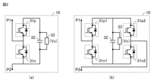
- FIG. 2 is a circuit diagram showing an example of a converter cell.
- FIG. 2 is a diagram showing an example of a hardware configuration of a control device.
- FIG. 2 is a block diagram showing an example of a functional configuration of a control device.
- FIG. 2 is a block diagram showing an example of a functional configuration of a correction voltage generation section according to the first embodiment.
- 7 is a block diagram illustrating an example of a functional configuration of a correction voltage generation section according to a second embodiment.
- FIG. FIG. 3 is a block diagram showing an example of a functional configuration of a system voltage control section according to a second embodiment.
- FIG. 7 is a block diagram showing an example of a functional configuration of a correction voltage generation section according to a third embodiment.
- FIG. 7 is a block diagram showing an example of a functional configuration of a current suppressor according to a third embodiment.
- FIG. 7 is a block diagram illustrating a transfer function of a controlled object of a power conversion device according to a third embodiment.
- FIG. 1 is a diagram for explaining an example of the overall configuration of a power conversion system.
- Power conversion system 1000 includes a power system 2 , an interconnection transformer 3 , an AC current detector 6 , an AC voltage detector 7 , and a power conversion device 200 .
- Power conversion device 200 includes a control device 100 and a power converter 20.
- a power converter 20 having a delta-connected three-phase arm is connected in parallel to a three-phase power system 2 via a three-phase interconnection transformer 3.
- the power converter 20 and the power system 2 may be connected via a interconnection reactor (not shown).
- the power converter 20 has an arm 4 for each phase: U phase, V phase, and W phase.
- Each arm 4 is configured by connecting N converter cells 10 (N: a natural number of 2 or more) cascade-connected to each other and an arm reactor 5 in series.
- N a natural number of 2 or more
- the arms 4 of each phase are interconnected in a delta connection. As described above, the connection ends of the arms 4 of each phase are connected to the power system 2 via the "reactor component" represented by the interconnection transformer 3.
- the arm reactor 5 is inserted to suppress the circulating current that passes through two or more arms 4 and circulates within the power converter 20.
- the arm reactor 5 can be placed at any location as long as it is connected in series with the converter cell 10, and a plurality of arm reactors may be inserted in a distributed manner.
- FIG. 2 is a circuit diagram showing an example of the converter cell 10.
- the converter cell 10 shown in FIG. 2(a) has a circuit configuration called a half-bridge configuration.
- This converter cell 10 includes a series body formed by connecting two switching elements 31p and 31n in series, a capacitor 32 as a power storage element, and a voltage detector 33.
- the series body and capacitor 32 are connected in parallel.
- Voltage detector 33 detects Vc (hereinafter also referred to as capacitor voltage Vc) indicating the DC voltage across capacitor 32 .
- the converter cell 10 shown in FIG. 2(b) has a circuit configuration called a full-bridge configuration.
- This converter cell 10 includes a first series body formed by connecting two switching elements 31p1 and 31n1 in series, and a second series body formed by connecting two switching elements 31p2 and 31n2 in series. , a capacitor 32, and a voltage detector 33.
- the first series body, the second series body, and the capacitor 32 are connected in parallel.
- Voltage detector 33 detects capacitor voltage Vc.
- the two switching elements 31p, 31n in FIG. 2(a) and the four switching elements 31p1, 31n1, 31p2, 31n2 in FIG. 2(b) are, for example, IGBT, GCT thyristor, MOSFET (Metal Oxide Semiconductor Field-Effect). It consists of a self-extinguishing semiconductor switching element such as a transistor, and a freewheeling diode connected in antiparallel. Further, in FIGS. 2(a) and 2(b), a capacitor such as a film capacitor is mainly used as the capacitor 32.
- the switching elements 31p, 31n, 31p1, 31n1, 31p2, and 31n2 are also collectively referred to as the switching element 31. Further, turning on/off of the semiconductor switching element in the switching element 31 will be simply referred to as "on/off of the switching element 31".
- both terminals of the switching element 31n are designated as input/output terminals P1 and P2.
- a voltage across the capacitor 32 and a zero voltage are outputted by the switching operations of the switching elements 31p and 31n. For example, when the switching element 31p is turned on and the switching element 31n is turned off, the voltage across the capacitor 32 is output. When the switching element 31p is turned off and the switching element 31n is turned on, zero voltage is output.
- the midpoint between switching element 31p1 and switching element 31n1 and the midpoint between switching element 31p2 and switching element 31n2 are connected to input/output terminal P1 of converter cell 10, respectively. Let it be P2.
- the converter cell 10 shown in FIG. 2(b) outputs a positive voltage or zero voltage by turning on the switching element 31n2, turning off the switching element 31p2, and alternately turning on the switching elements 31p1 and 31n1. . Further, the converter cell 10 shown in FIG. 2(b) can generate zero voltage or negative voltage by turning off the switching element 31n2, turning on the switching element 31p2, and turning on the switching elements 31p1 and 31n1 alternately. Can be output.
- the converter cell 10 has, for example, a full-bridge cell configuration shown in FIG. 2(b), and uses a semiconductor switching element and a capacitor as a power storage element.
- the converter cell 10 may have a half-bridge configuration as shown in FIG. 2(a).
- a converter cell having a configuration other than that shown above, for example, a converter cell employing a circuit configuration also called a 1.5 half-bridge configuration in which the switching element 31p2 in FIG. 2(b) is replaced with only a diode may also be used. good.
- power converter 20 further includes arm current detectors 40 arranged corresponding to arms 4 of each phase.
- Arm current detector 40 detects arm currents Iu, Iv, and Iw passing through arm 4 of each phase.
- the AC current detector 6 detects three-phase AC currents Isysu, Isysv, and Isysw (hereinafter also collectively referred to as "AC current Isys") of the power system 2.
- AC current Isys corresponds to the "output current” from the power converter 20 to the power system 2.
- the AC voltage detector 7 detects three-phase AC voltages Vsysu, Vsysv, and Vsysw (hereinafter also collectively referred to as "AC voltage Vsys”) of the power system 2.
- Each detection value of AC current detector 6 and AC voltage detector 7 is input to control device 100 .
- the control device 100 is a device that controls the power converter 20. Control device 100 controls on/off of each switching element 31 of each converter cell 10 to operate power converter 20 as a voltage source according to an operation command value. The specific functional configuration of the control device 100 will be described later.
- FIG. 3 is a diagram showing an example of the hardware configuration of the control device 100.
- FIG. 3 shows an example in which the control device 100 is configured by a computer.
- control device 100 includes one or more input converters 70, one or more sample and hold (S/H) circuits 71, multiplexer 72, A/D converter 73, It includes at least one CPU (Central Processing Unit) 74, a RAM (Random Access Memory) 75, a ROM (Read Only Memory) 76, one or more input/output interfaces 77, and an auxiliary storage device 78.
- Control device 100 also includes a bus 79 that interconnects the components.
- the input converter 70 has an auxiliary transformer for each input channel.
- Each auxiliary transformer converts the detection signal from each detector of FIG. 1 into a signal at a voltage level suitable for subsequent signal processing.
- the S/H circuit 71 is provided for each input converter 70.
- the S/H circuit 71 samples and holds a signal representing the amount of electricity received from the corresponding input converter 70 at a specified sampling frequency.
- the multiplexer 72 sequentially selects the signals held in the plurality of sample and hold circuits 71.
- A/D converter 73 converts the signal selected by multiplexer 72 into a digital value. Note that by providing a plurality of A/D converters 73, A/D conversion may be performed in parallel on detection signals of a plurality of input channels.
- the CPU 74 controls the entire control device 100 and executes arithmetic processing according to a program.
- RAM 75 as a volatile memory
- ROM 76 as a non-volatile memory are used as main memory of the CPU 74.
- the ROM 76 stores programs, signal processing settings, and the like.
- the auxiliary storage device 78 is a non-volatile memory with a larger capacity than the ROM 76, and stores programs, data of the detected amount of electricity, and the like.
- the input/output interface 77 is an interface circuit for communicating between the CPU 74 and external devices.
- control device 100 may be configured using circuits such as FPGA (Field Programmable Gate Array) and ASIC (Application Specific Integrated Circuit).
- FPGA Field Programmable Gate Array
- ASIC Application Specific Integrated Circuit
- FIG. 4 is a block diagram showing an example of the functional configuration of the control device.
- control device 100 includes a phase balance control section 210, a circulating current control section 220, a reference voltage command generation section 230, a correction voltage generation section 240, a voltage command calculation section 250, and a gate signal generation unit 260.
- the processing circuit may be dedicated hardware or may be a CPU that executes a program stored in the internal memory of the control device 100.
- the processing circuit is configured of, for example, an FPGA, an ASIC, or a combination thereof.
- the phase balance control unit 210 generates arm current command values Iu*, Iv*, Iw* for each phase based on the DC voltage of the capacitor 32 of each converter cell 10 (that is, the capacitor voltage Vc).
- the phase balance control unit 210 calculates a balance voltage command value Vcph for controlling the balance voltage of each phase based on the capacitor voltages Vc of all converter cells 10.
- Balance voltage command value Vcph may be set to, for example, the average value, median value, maximum value, or minimum value of capacitor voltages Vc of all converter cells 10.
- the phase balance control unit 210 calculates representative voltage values Vcu, Vcv, and Vcw of the capacitor voltage Vc for each capacitor 32 of the N converter cells 10 of the U phase, V phase, and W phase.
- the representative voltage values Vcu, Vcv, and Vcw may also be set to the average value, median value, maximum value, or minimum value of the capacitor voltages Vc of the N converter cells 10 of the same phase. Note that since the representative voltage values Vcu, Vcv, and Vcw of each phase oscillate at 2f (where f is the fundamental frequency), the filter removes the 2f AC component and leaves only the DC component.
- the phase balance control unit 210 calculates deviations ⁇ Vcu, ⁇ Vcv, and ⁇ Vcw between the balance voltage command value Vcph and the representative voltage values Vcu, Vcv, and Vcw of each phase.
- ⁇ Vcu Vcph ⁇ Vcu
- ⁇ Vcv Vcph ⁇ Vcv
- ⁇ Vcw Vcph ⁇ Vcw.
- the phase balance control unit 210 calculates arm current command values Iu*, Iv*, Iw* for each phase so that the representative voltage values Vcu, Vcv, and Vcw of each phase follow the balance voltage command value Vcph. That is, the phase balance control unit 210 executes a feedback calculation to make the deviations ⁇ Vcu, ⁇ Vcv, and ⁇ Vcw smaller than the specified values (for example, set each deviation to 0), thereby adjusting the arm current command value Iu of each phase. *, Iv*, Iw* are generated.
- the phase balance control section 210 may be configured by, for example, a proportional controller, a PI controller, a PID controller, or another controller used for feedback control. The control by the phase balance control section 210 corresponds to interphase balance voltage control that makes the representative value of each phase voltage match the command value.
- the arm current command values Iu*, Iv*, Iw* of each phase and the arm currents Iu, Iv, Iw of each phase detected by the arm current detector 40 are input to the circulating current control unit 220. .
- the circulating current control unit 220 generates a circulating current command value Iz* for controlling the circulating current Iz based on the arm current command values Iu*, Iv*, Iw* of each phase.
- the circulating current control unit 220 uses the arm current command values Iu*, Iv*, and Iw* of each phase to calculate the circulating current command value Iz* according to the following equation (1).
- the circulating current control unit 220 uses the detected arm currents Iu, Iv, and Iw of each phase to calculate the circulating current Iz according to the following equation (2).
- the circulating current control unit 220 generates a circulating voltage command value Vz* that causes the circulating current Iz to follow the circulating current command value Iz*. That is, the circulating current control unit 220 generates the circulating voltage command value Vz* by executing a feedback calculation to make the deviation ⁇ Iz smaller than the specified value (for example, make the deviation ⁇ Iz 0).
- the circulating current control unit 220 may be configured by, for example, a proportional controller, a PI controller, a PID controller, or another controller used for feedback control.
- the reference voltage command generation unit 230 generates a d-axis reference voltage command value Vd* and a d-axis reference voltage command value Vd* in a two-axis (i.e., dq-axis) rotating coordinate system as a reference voltage command value for operating the power converter 20 as a voltage source. Generate a q-axis reference voltage command value Vq*.
- the reference voltage command generation unit 230 generates reference voltage command values Vd* and Vq* (hereinafter also collectively referred to as "reference voltage command values V*") for simulating the behavior when the synchronous generator is connected to the power system. ) can be created by any known technique.
- the voltage command value of the dq axis obtained by converting the voltage command value generated in a state where the operation of the output current suppressor is stopped and the internal impedance is kept constant is converted from three-phase to two-phase. may be used as reference voltage command values Vd*, Vq*.
- the reference voltage command value V* does not have to be a voltage command value for operating as a virtual synchronous machine.
- the reference voltage command generation unit 230 performs three-phase/two-phase conversion on the AC voltages Vsysu, Vsysv, and Vsysw using the reference phase ⁇ , and calculates the d-axis voltage Vd and the q-axis voltage Vq.
- the reference phase ⁇ is a reference phase used to control the power converter 20.
- the reference voltage command generation unit 230 generates the reference voltage command value Vd* through feedback control to zero the deviation between the d-axis voltage Vd and the d-axis voltage command value Vdt (for example, an invalid component of the target voltage). .
- the reference voltage command generation unit 230 generates the reference voltage command value Vq* by feedback control to zero the deviation between the q-axis voltage Vq and the q-axis voltage command value Vqt (for example, the effective component of the target voltage). .
- the d-axis voltage command value Vdt and the q-axis voltage command value Vqt are, for example, values set in advance by a system operator or the like.
- the correction voltage generation unit 240 corrects the reference voltage command values Vd*, Vq* of the power converter 20 using correction values for suppressing overcurrent due to voltage imbalance in the power system 2, thereby generating a correction voltage.
- Command values Vda*, Vqa* (hereinafter also collectively referred to as "corrected voltage command value Va*") are generated.
- the detailed configuration of the correction voltage generation section 240 will be described later.
- the gate signal generation unit 260 calculates the output voltage command values Vucell*, Vvcell*, Vwcell* of the converter cell 10 of each phase based on the arm voltage command values Vu*, Vv*, Vw* of each phase.
- the gate signal generation unit 260 executes PWM (Pulse Width Modulation) control based on the output voltage command values Vucell*, Vvcell*, and Vwcell* to control on/off driving of the switching element 31 of each converter cell 10 of each phase.
- PWM Pulse Width Modulation
- the gate signal generation unit 260 generates a PWM modulation signal by comparing the output voltage command value Vucell* with a carrier signal CS from a carrier generator (not shown).
- the carrier signal CS is composed of a periodic signal such as a triangular wave.
- the PWM modulation signal When the voltage of the output voltage command value Vucell* is higher than the voltage of the carrier signal CS, the PWM modulation signal is set to high level. On the contrary, when the voltage of the carrier signal CS is higher than the output voltage command value Vucell*, the PWM modulation signal is set to low level.
- the carrier signal CS is generated to mutually shift the timing of the PWM signals among the N converter cells 10 of each phase so as to realize phase-shifted PWM control.
- the gate signal generation unit 260 also generates the output voltage command value Vvcell* of each V-phase converter cell 10 and the output voltage command value Vwcell* of each W-phase converter cell 10 in the same manner as described above. Thereby, the gate signal generation section 260 generates a gate signal for controlling on/off of each of the switching elements 31 included in the converter cell 10 based on the PWM modulation signal. Each switching element 31 of each converter cell 10 is turned on and off according to the gate signal.
- FIG. 5 is a block diagram showing an example of the functional configuration of the correction voltage generation section 240A according to the first embodiment.
- a correction voltage generation section 240A corresponds to the correction voltage generation section 240 of FIG. 4, but is given the reference numeral "A" for convenience. This also applies to the second and third embodiments below.
- the correction voltage generation unit 240A calculates a correction value by applying filter processing to the AC voltage Vsys of the power system 2 to remove a DC component, and adds the correction value to the reference voltage command value V*.
- a corrected voltage command value Va* is generated.
- the correction voltage generation section 240A includes a coordinate transformation section 41, filters 42 and 43, and adders 44 and 45.
- the coordinate conversion unit 41 performs three-phase/two-phase conversion on the AC voltages Vsysu, Vsysv, and Vsysw using the reference phase ⁇ , and calculates the d-axis voltage Vd and the q-axis voltage Vq.
- the filter 42 calculates the d-axis voltage Vdh by removing the DC component of the d-axis voltage Vd by performing high-pass filter processing on the d-axis voltage Vd.
- Filter 43 calculates q-axis voltage Vqh from which the DC component of q-axis voltage Vq has been removed by performing high-pass filter processing on q-axis voltage Vq.
- the filters 42 and 43 may be filters that can remove DC components of the d-axis voltage Vd and the q-axis voltage Vq, respectively, and may be filters other than high-pass filters.
- the adder 44 adds the d-axis voltage Vdh to the d-axis component of the reference voltage command value (i.e., the reference voltage command value Vd*) to obtain the d-axis component of the corrected voltage command value (i.e., the corrected voltage command value Vda*). generate.
- the adder 45 adds the q-axis voltage Vqh to the q-axis component of the reference voltage command value (i.e., the reference voltage command value Vq*) to obtain the q-axis component of the corrected voltage command value (i.e., the corrected voltage command value Vqa*). generate.
- the d-axis voltage Vdh corresponds to the d-axis component of the correction value for correcting the reference voltage command value Vd*.
- the q-axis voltage Vqh corresponds to the q-axis component of the correction value for correcting the reference voltage command value Vq*.
- Embodiment 1 To facilitate understanding of the effects of the first embodiment, a case will be described in which the d-axis voltage Vdh and the q-axis voltage Vqh are not added to the reference voltage command value.
- the power converter 20 operates according to the arm voltage command value that reflects the reference voltage command values Vd*, Vq*.
- the power converter 20 does not depend on the grid voltage according to the reference voltage command values generated by a prescribed generation method (for example, the reference voltage command values Vd*, Vq* generated by the reference voltage command generation unit 230). Operates as a voltage source.
- the d-axis voltage Vdh and the q-axis voltage Vqh from which the DC component has been removed are fed forward and added to the reference voltage command values Vd*, Vq*. and corrected voltage command values Vda* and Vqa* are generated.
- the power converter 20 operates according to the arm voltage command value that reflects the corrected voltage command values Vda* and Vqa*.
- the system voltage includes only positive phase components.
- the positive phase component of the system voltage corresponds to the DC component, so the d-axis voltage Vd and the q-axis voltage Vq include only the DC component.
- the power converter 20 operates as a voltage source independent of the grid voltage according to the reference voltage command values (that is, the reference voltage command values Vd*, Vq*) generated by a prescribed generation method.
- the system voltage when voltage imbalance occurs in the power system 2, the system voltage includes a positive phase component and other components.
- the d-axis voltage Vd and the q-axis voltage Vq include a DC component and other components.
- the filters 42 and 43 perform filter processing to remove DC components from the d-axis voltage Vd and q-axis voltage Vq, the calculated d-axis voltage Vdh and q-axis voltage Vqh are free from other components other than the DC component. including.
- the corrected voltage command value Vda* is an added value of the reference voltage command value Vd* and the d-axis voltage Vdh including other components.
- the corrected voltage command value Vqa* is an added value of the reference voltage command value Vq* and the q-axis voltage Vqh including other components.
- a corrected voltage command value is generated that reflects the reference voltage command value for the positive phase component, and reflects other components of the system voltage for components other than the positive phase component.
- the power converter 20 By operating as a voltage source according to such a corrected voltage command value, the power converter 20 operates as a voltage source regarding the positive phase component, while maintaining the same voltage as the grid voltage regarding other components (for example, negative phase component). Output other components like. Therefore, even when the voltage is unbalanced, other component currents (for example, negative phase current) flowing from the power system 2 can be suppressed, and as a result, overcurrent in the power converter 20 can be suppressed.
- other component currents for example, negative phase current
- the power converter 20 operates as a voltage source, and can suppress the current flowing from the power system 2 for components other than the positive phase component. Therefore, even when the voltage is unbalanced, overcurrent in the power converter 20 can be prevented, and the continuity of operation of the power converter 20 can be improved.
- FIG. 6 is a block diagram showing an example of the functional configuration of the correction voltage generation section 240B according to the second embodiment.
- correction voltage generation unit 240B calculates an amplitude correction value for correcting the amplitude of reference voltage command value V* based on AC voltage Vsys of power system 2.
- the corrected voltage generation unit 240B When voltage unbalance in the power system 2 has not occurred, the corrected voltage generation unit 240B generates the corrected voltage command value Va* by adding the amplitude correction value to the amplitude of the reference voltage command value V*.
- the corrected voltage generation unit 240B When voltage imbalance occurs in the power system 2, the corrected voltage generation unit 240B generates the corrected voltage command value Va* by adding a value smaller than the amplitude correction value to the amplitude of the reference voltage command value.
- the correction voltage generation section 240B includes coordinate conversion sections 51, 53, 58, 60, amplitude calculation sections 52, 54, judgment section 55, system voltage control section 56, multiplier 57, and addition 59.
- the coordinate conversion unit 51 performs three-phase/two-phase conversion on the AC voltages Vsysu, Vsysv, and Vsysw using the reference phase ⁇ , and calculates the positive-phase d-axis voltage Vd and q-axis voltage Vq.
- the coordinate conversion unit 53 converts the alternating current voltages Vsysu, Vsysv, and Vsysw into three-phase/two-phase using the negative phase "- ⁇ " of the reference phase ⁇ , and converts the AC voltages Vsysu, Vsysv, and Vsysw into opposite-phase d-axis voltage Vdn and q-axis voltage Vqn. Calculate.
- the amplitude calculation unit 52 calculates a positive-sequence voltage amplitude Vmag_p, which is the amplitude of the d-axis voltage Vd and the q-axis voltage Vq. Specifically, the amplitude calculation unit 52 removes high frequency components of the d-axis voltage Vd and q-axis voltage Vq using a moving average filter or the like, and calculates the sum of squares of the removed d-axis voltage Vd and q-axis voltage Vq (i.e. , (Vd 2 +Vq 2 ) 1/2 ). The amplitude calculation unit 52 outputs the sum of squares as a positive-sequence voltage amplitude Vmag_p.
- the amplitude calculation unit 54 calculates a negative phase voltage amplitude Vmag_n, which is the amplitude of the d-axis voltage Vdn and the q-axis voltage Vqn. Specifically, the amplitude calculation unit 54 removes the high frequency components of the d-axis voltage Vdn and the q-axis voltage Vqn using a moving average filter or the like, and calculates the sum of squares of the removed d-axis voltage Vdn and q-axis voltage Vqn (i.e. , (Vdn 2 +Vqn 2 ) 1/2 ). The amplitude calculation unit 54 outputs the sum of squares as the negative phase voltage amplitude Vmag_n.
- the determining unit 55 determines whether voltage imbalance has occurred in the power system 2 based on the positive-sequence voltage amplitude Vmag_p and the negative-sequence voltage amplitude Vmag_n. Specifically, the determining unit 55 determines whether the conditions that the positive phase voltage amplitude Vmag_p is less than the threshold value Vthp and the negative phase voltage amplitude Vmag_n is greater than or equal to the threshold value Vthn are satisfied.
- the determining unit 55 determines that voltage imbalance has occurred in the power system 2, and outputs a constant Kth.
- the constant Kth is greater than or equal to 0 and less than 1, and is typically 0.
- the determining unit 55 determines that voltage unbalance has not occurred, and outputs a value of "1".
- the constant Kth is a value of 0 or more and 1 or less.
- the determining unit 55 outputs a larger constant Kth as the difference ⁇ Vmag is larger.
- the constant Kth is "1" in a normal state where no voltage unbalance occurs, and the constant Kth is "0" when a large voltage unbalance occurs.
- the system voltage control unit 56 generates a voltage amplitude correction amount ⁇ Vam for correcting the amplitude of the reference voltage command value V* in order to make the AC voltage Vsys follow the target voltage.
- FIG. 7 is a block diagram showing an example of the functional configuration of the system voltage control section according to the second embodiment.
- the system voltage control section 56 includes subtracters 82 and 83 and an amplitude correction section 84.
- the subtracter 82 calculates the deviation ⁇ Vp between the system voltage command value Vref and the positive-sequence voltage amplitude Vmag_p.
- the subtracter 83 calculates a deviation ⁇ Q between the reactive power command value Qref and the reactive power Q of the power system 2.
- the amplitude correction unit 84 selects either automatic voltage adjustment mode or automatic reactive power adjustment mode, and generates voltage amplitude correction amount ⁇ Vam based on the selected mode. Specifically, when the automatic voltage adjustment mode is selected, the amplitude correction unit 84 generates the amplitude correction amount ⁇ Vam through feedback control to reduce the deviation ⁇ Vp. When the automatic reactive power adjustment mode is selected, the amplitude correction unit 84 generates the amplitude correction amount ⁇ Vam through feedback control to make the deviation ⁇ Q zero.
- the amplitude correction section 84 includes a PI controller, a first-order lag element, and the like.
- multiplier 57 calculates a multiplier value ⁇ Vamx of the amplitude correction amount ⁇ Vam output from system voltage control unit 56 and the value output from determination unit 55 (i.e., constant Kth or 1). Output. For example, when voltage unbalance does not occur, the output value from the determination unit 55 is “1”, and when voltage unbalance occurs, the output value from the determination unit 55 is “0”. If so, the multiplication value ⁇ Vamx is ⁇ Vam when voltage unbalance has not occurred, and the multiplication value ⁇ Vamx is 0 when voltage unbalance has occurred.
- the coordinate conversion unit 58 converts the reference voltage command value Vd* and the reference voltage command value Vq* into amplitude
- the phase ⁇ matches the reference phase ⁇ .
- the adder 59 outputs an added value obtained by adding the amplitude
- the coordinate conversion unit 60 performs dq-axis conversion on the added value and the phase ⁇ to generate corrected voltage command values Vda*, Vqa*.
- Embodiment 2 typically, when voltage unbalance in the power system 2 does not occur, the multiplication value ⁇ Vamx added to the amplitude
- the power converter 20 outputs reactive power according to the amplitude correction amount ⁇ Vam to perform automatic control of the grid voltage.
- the power converter 20 does not output reactive power according to the amplitude correction amount ⁇ Vam, and does not perform automatic control of the system voltage. This is to suppress the unbalance of the capacitor voltages of each phase when the voltage is unbalanced, and to suppress the overcurrent of the power converter 20.
- the power converter 20 performs automatic control of the grid voltage by outputting reactive power according to the amplitude correction amount ⁇ Vam when the voltage is unbalanced.
- the capacitor voltages of each phase become unbalanced. Therefore, the circulating current command value Iz* based on the arm current command values Iu*, Iv*, Iw* from the phase balance control unit 210 does not become 0, and in order to eliminate the imbalance, the circulating current command value Iz* is A circulating current Iz flows within the power converter 20. That is, the larger the voltage unbalance, the larger the reactive power output, and the larger the circulating current Iz. As a result, an overcurrent occurs and the power converter 20 comes to a protective stop.
- the automatic grid voltage control function is enabled when voltage unbalance does not occur, but the automatic grid voltage control function is stopped when voltage unbalance occurs. to suppress overcurrent. Therefore, the continuity of operation of the power converter 20 can be improved even when the voltage is unbalanced.
- FIG. 8 is a block diagram showing an example of the functional configuration of the correction voltage generation section 240C according to the third embodiment.
- correction voltage generation section 240C calculates negative phase current command values Idn*, Iqn* based on arm current command values Iu*, Iv*, Iw* of each phase. Subsequently, the correction voltage generation unit 240C converts the output current into a current based on the detected value of the output current from the power converter 20 (that is, the alternating current Isys) and the negative phase current command values Idn*, Iqn*. Calculate voltage correction values ⁇ Vda and ⁇ Vqa for suppressing the voltage to below the limit value. Furthermore, the corrected voltage generation unit 240C generates corrected voltage command values Vda*, Vqa* by adding the voltage correction values ⁇ Vda, ⁇ Vqa to the reference voltage command values Vd*, Vq*, respectively.
- the correction voltage generation section 240C includes a negative phase current command calculation section 91, a current suppression section 92, and adders 93 and 94.
- the negative phase current command calculation unit 91 adds the arm current command values Iu*, Iv*, Iw* of each phase, divides the added value by 3, and obtains the circulating current command value. Calculate Iz*.
- the negative phase current command calculation unit 91 calculates a value R1 obtained by performing three-phase/two-phase coordinate transformation on the extracted positive phase component and negative phase component.
- the negative phase current command calculating section 91 calculates the value R2 by performing filter processing to extract the positive phase component from the value R1.
- the negative phase current command calculation unit 91 calculates negative phase current command values Idn*, Iqn* by subtracting the value R2 from the value R1.
- the filter used for extracting the positive phase component has a function of removing the negative phase component from the filter input value and extracting the positive phase component.
- the positive phase component is a DC component and the negative phase component is a frequency component (2f) twice the fundamental frequency, so a first-order lag, a 2f moving average, a 2f notch filter, etc. are used.
- the current suppressor 92 reduces the output current to a current limit value or less based on the detected value of the output current from the power converter 20 (i.e., the alternating current Isys) and the negative phase current command values Idn*, Iqn*. Voltage correction values ⁇ Vda and ⁇ Vqa for suppression are calculated.
- FIG. 9 is a block diagram showing an example of the functional configuration of the current suppressor according to the third embodiment.
- current suppression section 92 includes a coordinate conversion section 110, a current command value generation section 120, a deviation calculation section 130, and a control calculation section 190.
- the coordinate conversion unit 110 performs three-phase/two-phase conversion on the detected value of the alternating current Isys to calculate the d-axis current Id and the q-axis current Iq.
- the current command value generation unit 120 generates a d-axis current command value Id* and a q-axis current command value Iq* based on the d-axis current Id and the q-axis current Iq, and the current limit value Imax.
- current command value generation section 120 includes coordinate conversion sections 121 and 122 and a limiter 125.
- the coordinate transformation unit 121 outputs a current amplitude Imag and a current phase ⁇ i by performing polar coordinate (r ⁇ ) transformation on the d-axis current Id and the q-axis current Iq on the dq axes.
- the current amplitude Imag and current phase ⁇ i are expressed by the following equations (3) and (4) using the d-axis current Id and the q-axis current Iq.
- the limiter 125 outputs the current limit value Imax. Further, the limiter 125 outputs the current amplitude Imag from the coordinate conversion unit 121 when the current amplitude Imag is less than the current limit value Imax (that is, Imag ⁇ Imax).
- the explanation will proceed assuming that the current amplitude of the alternating current Isys and the current amplitude Imag obtained by equation (3) are equal, so the upper limit value of the limiter 125 is set to the same value as the current limit value of the alternating current Isys. be done.
- the three-phase/two-phase conversion in the coordinate conversion unit 110 is performed so that the current amplitude of the alternating current Isys is K times (K: constant) the current amplitude Imag on the dq axis obtained by equation (3).
- the upper limit value of limiter 125 is set to (1/K) times the current limit value Imax.
- the coordinate conversion unit 122 uses the output value from the limiter 125 as the amplitude, converts the current phase ⁇ i output from the coordinate conversion unit 121 from polar coordinates to dq coordinates, and converts the d-axis current command value Id* and the q-axis Generate current command value Iq*.
- the ratio of Iq* to Id* (i.e., Iq*/Id*), which corresponds to the phase of the d-axis current command value Id* and the q-axis current command value Iq*, is the d-axis current command value generated from the detected value of the alternating current Isys. It is the same as the ratio of q-axis current Iq to current Id (ie, Iq/Id).
- the amplitudes of the d-axis current command value Id* and the q-axis current command value Iq* are limited by the limiter 125 to below the current limit value Imax.
- the current command value generation unit 120 sets the d-axis current Id and the q-axis current Iq to They are generated as a d-axis current command value Id* and a q-axis current command value Iq*, respectively.
- the current command value generation unit 120 converts the d-axis current value and q-axis current value corresponding to the current limit value Imax into the d-axis current command value and the q-axis current value, respectively. Generate as a current command value. Specifically, the d-axis current command value Id* and the q-axis current command value Iq* have an amplitude (that is, (Id* 2 + Iq* 2 ) 1/2 ) of the current limit value Imax, and Id* The ratio of Id and Iq* is set to be the same as the ratio of Id and Iq.
- the deviation calculation unit 130 calculates a current deviation ⁇ Id between the d-axis current command value Id* and the d-axis component of the negative-sequence current command value (that is, the negative-sequence current command value Idn*) and the d-axis current. . In addition, the deviation calculation unit 130 calculates a current deviation ⁇ Iq between the q-axis current command value Iq* and the q-axis component of the negative-phase current command value (that is, the negative-phase current command value Iqn*) and the q-axis current. calculate.
- the deviation calculation unit 130 includes adders 131 and 132 and subtracters 133 and 134.
- Adder 131 adds d-axis current command value Id* and negative phase current command value Idn*.
- the subtracter 133 subtracts the d-axis current Id from the added value (Id*+Idn*) by the adder 131 to calculate the current deviation ⁇ Id.
- Adder 132 adds q-axis current command value Iq* and negative phase current command value Iqn*.
- the subtracter 134 subtracts the q-axis current Iq from the added value (Iq*+Iqn*) by the adder 132 to calculate a current deviation ⁇ Iq.
- the control calculation unit 190 calculates a voltage correction value ⁇ Vda to compensate for the current deviation ⁇ Id and a voltage correction value ⁇ Vqa to compensate for the current deviation ⁇ Iq.
- ⁇ Vda is the d-axis component of the voltage correction value
- ⁇ Vqa is the q-axis component of the voltage correction value.
- the control calculation section 190 includes a proportional control section 140 and a correction value calculation section 150.
- the proportional control section 140 has proportional devices 141 and 142.
- the correction value calculation unit 150 calculates a voltage correction value ⁇ Vda and a voltage correction value ⁇ Vqa. Specifically, the correction value calculation unit 150 calculates the voltage correction value ⁇ Vda based on the multiplication value MP1 and the integral value of the multiplication value MP2, and calculates the voltage correction value ⁇ Vda based on the multiplication value MP2 and the integral value of the multiplication value MP1. Then, a voltage correction value ⁇ Vqa is calculated. Specifically, the correction value calculation unit 150 includes integrators 151 and 152 with a time constant Tc, a subtracter 161, an adder 162, and multipliers 171 and 172.
- the integrator 151 outputs the integral value of the multiplication value MP1 output from the proportional device 141 to the adder 162.
- the integrator 152 outputs the integral value of the multiplication value MP2 output from the proportional device 142 to the subtracter 161.
- the subtracter 161 outputs a subtracted value obtained by subtracting the integral value of the multiplication value MP2 from the multiplication value MP1.
- the adder 162 outputs a sum value obtained by adding the multiplication value MP2 and the integral value of the multiplication value MP1.
- the multiplier 171 outputs the value obtained by multiplying the output value of the subtracter 161 by the adjustment gain Kcmp as the voltage correction value ⁇ Vda of the d-axis component of the reference voltage command value (i.e., the reference voltage command value Vd*).
- Multiplier 172 outputs a value obtained by multiplying the output value of adder 162 by adjustment gain Kcmp as voltage correction value ⁇ Vqa of the q-axis component of reference voltage command value (that is, reference voltage command value Vq*).
- adder 93 calculates the d-axis component of the corrected voltage command value (i.e., corrected voltage command value Vda*) by adding the reference voltage command value Vd* and the voltage correction value ⁇ Vda. calculate.
- the adder 94 calculates the q-axis component of the corrected voltage command value (ie, the corrected voltage command value Vqa*) by adding the reference voltage command value Vq* and the voltage correction value ⁇ Vqa.
- the current suppression control by the current suppression unit 92 includes the correction value calculation unit 150 causing the current deviation ⁇ Id to act on the voltage correction value ⁇ Vqa, and also causing the current deviation ⁇ Iq to act on the voltage correction value ⁇ Vda.
- the non-interference between the d and q axes is performed by integral control.
- FIG. 10 is a block diagram illustrating a transfer function of a controlled object of the power conversion device according to the third embodiment.
- the transfer function of the controlled object 22 whose input is the output voltage of the power converter 20 and whose output is the alternating current Isys detected by the alternating current detector 6 is shown on the dq coordinate axis. . That is, the input to the controlled object 22 is represented by a d-axis voltage Vd and a q-axis voltage Vq obtained by converting the output voltage of the power converter 20 from three-phase to two-phase.
- the output of the controlled object 22 is represented by a d-axis current Id and a q-axis current Iq obtained by converting the alternating current Isys detected by the alternating current detector 6 into three-phase/two-phase.
- the d-axis current Id and the q-axis current Iq correspond to the output values of the coordinate conversion section 110 in FIG. 9.
- the controlled object 22 corresponds to a combination of the impedances of the power converter 20 and the power system 2. Therefore, on the dq coordinate axis, the resistance component Rc and inductance component Lc of the power converter 20, the resistance component Rs and inductance component Ls of the power system 2, and the angular frequency of the output voltage (AC voltage) of the power converter 20 Transfer functions 26d, 26q, 27d, 27q, 28, and 29 between the d-axis voltage Vd, q-axis voltage Vq, and the d-axis current Id, q-axis current Iq are determined using ⁇ .
- Transfer functions 26d and 27d indicate the interaction between the d-axis voltage Vd and the d-axis current Id
- transfer functions 26q and 27q indicate the interaction between the q-axis voltage Vq and the q-axis current Iq.
- the interaction caused by the transfer functions 26d and 27d can be compensated for by feedback control that calculates the corrected voltage command value Vda* using the current deviation ⁇ Id.
- the interaction caused by the transfer functions 26q and 27q can also be compensated for by feedback control that calculates the corrected voltage command value Vqa* using the current deviation ⁇ Iq.
- the controlled object 22 further includes a transfer function 28 in which the d-axis current Id acts on the q-axis voltage Vq, and a transfer function 29 in which the q-axis current Iq acts on the d-axis voltage Vd. Therefore, the correction value calculation unit 150 performs non-interference such that the d-axis current deviation ⁇ Id is reflected in the corrected voltage command value Vqa*, and the q-axis current deviation ⁇ Iq is reflected in the corrected voltage command value Vda*. .
- the transfer functions 28 and 29 include the inductance component Ls of the power system 2.
- the inductance component Lc of the power converter 20 can be accurately estimated according to circuit constants, but the inductance component Ls depends on the status of the power system 2 (for example, load status, presence or absence of a ground fault, location of the ground fault, etc.) It is difficult to estimate accurately because it varies depending on
- the inductance component Ls of the power system 2 can be accurately estimated by calculating the voltage correction values ⁇ Vda and ⁇ Vqa with non-interference through integral control in the correction value calculation unit 150. Even if the current deviations ⁇ Id and ⁇ Iq are not set, the corrected voltage command values Vda* and Vqa* can be set to compensate for the current deviations ⁇ Id and ⁇ Iq and make them zero.
- the inductance component Ls of the power system 2 can be estimated accurately, it is also possible to realize non-interference control by proportional control using control gains set according to the transfer functions 28 and 29 instead of integral control.
- proportional control when performing non-interference control using proportional control, there is a concern that the estimation error of the inductance component Ls may destabilize the current suppression effect by the current suppression section 92.
- the current suppression effect by the current suppression unit 92 can be stabilized without requiring estimation of the inductance component Ls of the power system 2.
- the corrected voltage command values Vda*, Vqa* reflect the correction values ⁇ Vda, ⁇ Vqa for compensating the current deviations ⁇ Id, ⁇ Iq with respect to the reference voltage command values Vd*, Vq*. is generated. Furthermore, the negative phase current command values Idn*, Iqn* generated by the negative phase current command calculating section 91 are reflected in the current deviations ⁇ Id, ⁇ Iq.
- the current command values Id*, Iq* are used to control the amplitude of the alternating current Isys to be equivalent to the current limit value Imax.
- the current deviations ⁇ Id and ⁇ Iq are set according to the excess of the current amplitude due to the d-axis current Id and the q-axis current Iq with respect to the current limit value Imax.
- the current deviations ⁇ Id and ⁇ Iq reflect the negative phase current command values Idn* and Iqn*.
- the voltage correction values ⁇ Vda and ⁇ Vqa are calculated in the current suppressing section 92 so as to compensate for the current deviations ⁇ Id and ⁇ Iq, respectively. Thereby, the power converter 20 can suppress the positive sequence current and the negative sequence current.
- the configuration is such that the negative phase current command values Idn*, Iqn* are always added to the d-axis current command value Id* and the q-axis current command value Iq*, respectively. has been described, but the configuration is not limited to this.
- the negative phase current command value Idn* when the negative phase current command value Idn* is larger than the specified value X1, the negative phase current command value Idn* may be added to the d-axis current command value Id*.
- the negative phase current command value Iqn* is larger than the specified value X2, the negative phase current command value Iqn* may be added to the q-axis current command value Iq*.
Landscapes
- Engineering & Computer Science (AREA)
- Power Engineering (AREA)
- Inverter Devices (AREA)
Abstract
A power conversion device (200) comprises: a power converter (20) that includes a plurality of converter cells (10); and a control device (100). The control device (100) includes: a phase balance control unit (210) that generates an arm current command value for each phase on the basis of a direct current voltage of a power storage element (32) of each converter cell (10); a circulation current control unit (220) that generates a circulation voltage command value for controlling a circulation current, on the basis of the arm current command value of each phase; a corrected voltage generation unit (240) that generates a corrected voltage command value by using a correction value, which is for suppressing an overcurrent caused by voltage unbalance of a power system (2), to correct a reference voltage command value; a voltage command calculation unit (250) that generates an arm voltage command value for each phase on the basis of the circulation voltage command value and the corrected voltage command value; and a gate signal generation unit (260) that generates a control signal for each switching element (32) of each converter cell (10) of each arm (4) in accordance with the arm voltage command value for each phase.
Description
本開示は、電力変換装置、および制御装置に関する。
The present disclosure relates to a power conversion device and a control device.
近年、電力系統に対して、太陽光発電設備等の再生可能エネルギーを用いた多くの分散型電源が導入されている。分散型電源は、電力変換器を介して電力系統に接続される場合が多い。そのため、電力系統に接続される分散型電源が増加すると電力系統に接続される同期機の割合が減少し、電力系統内の慣性エネルギーが減少する。そこで、電力変換器に同期機と同様な挙動をさせることによって減少した慣性エネルギーを補う仮想同期機制御が提案されている。
In recent years, many distributed power sources using renewable energy such as solar power generation equipment have been introduced into power systems. Distributed power sources are often connected to the power grid via power converters. Therefore, as the number of distributed power sources connected to the power system increases, the proportion of synchronous machines connected to the power system decreases, and the inertial energy within the power system decreases. Therefore, virtual synchronous machine control has been proposed to compensate for the reduced inertial energy by causing the power converter to behave in the same way as a synchronous machine.
例えば、特開2019-80476号公報(特許文献1)に係る交直変換器制御装置は、蓄電池から出力される電力が同期発電機の特性と同等な特性となるように同期発電機特性を演算する発電機特性演算部と、電力系統に短絡事故が発生したとき交直変換器の出力電流が電流制限値を超えないように仮想同期発電機の内部インピーダンスを変化させる出力電流抑制部とを含む。
For example, the AC/DC converter control device according to Japanese Patent Application Publication No. 2019-80476 (Patent Document 1) calculates the synchronous generator characteristics so that the power output from the storage battery has the same characteristics as the synchronous generator characteristics. It includes a generator characteristic calculation section and an output current suppression section that changes the internal impedance of the virtual synchronous generator so that the output current of the AC/DC converter does not exceed a current limit value when a short circuit fault occurs in the power system.
特許文献1では、電圧源として動作する電力変換器において、電力系統に短絡事故が発生しても過電流によって保護停止することなく運転継続を可能とすることを検討している。しかし、特許文献1では、電圧源として動作する電力変換器がモジュラーマルチレベル変換器(MMC:Modular Multilevel Converter)で構成されている場合において、事故発生等による系統不平衡時に当該電力変換器を運転継続するための技術については何ら教示ないし示唆されていない。
Patent Document 1 considers enabling a power converter that operates as a voltage source to continue operating without protective shutdown due to overcurrent even if a short-circuit accident occurs in the power system. However, in Patent Document 1, when a power converter that operates as a voltage source is configured with a modular multilevel converter (MMC), the power converter is operated when the system is unbalanced due to an accident, etc. There is no teaching or suggestion of techniques for continuing.
本開示のある局面における目的は、電圧源として動作するMMC方式の電力変換器において、系統不平衡時の運転継続性を向上させることが可能な電力変換装置、および制御装置を提供することである。
An object of an aspect of the present disclosure is to provide a power converter and a control device that are capable of improving operational continuity during grid unbalance in an MMC power converter that operates as a voltage source. .
ある実施の形態に従うと、電力系統に接続された電力変換装置が提供される。電力変換装置は、互いにカスケード接続された複数の変換器セルを有するアームを少なくとも1つ含む電力変換器と、電力変換器を電圧源として動作させる制御装置とを備える。複数の変換器セルの各々は、複数のスイッチング素子と、複数のスイッチング素子に接続される蓄電要素とを含む。制御装置は、各変換器セルの蓄電要素の直流電圧に基づいて、各相のアーム電流指令値を生成する相バランス制御部と、各相のアーム電流指令値に基づいて、循環電流を制御する循環電圧指令値を生成する循環電流制御部と、電力系統の電圧不平衡による過電流を抑制するための補正値を用いて、電力変換器の基準電圧指令値を補正することにより、補正電圧指令値を生成する補正電圧生成部と、循環電圧指令値と補正電圧指令値とに基づいて、各相のアーム電圧指令値を生成する電圧指令演算部と、各相のアーム電圧指令値に従って各アームの各変換器セルの各スイッチング素子の制御信号を生成するゲート信号生成部とを含む。
According to an embodiment, a power conversion device connected to a power system is provided. The power converter includes a power converter including at least one arm having a plurality of converter cells cascade-connected to each other, and a control device that operates the power converter as a voltage source. Each of the plurality of converter cells includes a plurality of switching elements and a power storage element connected to the plurality of switching elements. The control device includes a phase balance control section that generates an arm current command value for each phase based on the DC voltage of the power storage element of each converter cell, and controls a circulating current based on the arm current command value for each phase. A corrected voltage command is generated by correcting the reference voltage command value of the power converter using a circulating current control unit that generates a circulating voltage command value and a correction value for suppressing overcurrent due to voltage imbalance in the power system. a voltage command calculation unit that generates an arm voltage command value for each phase based on the circulating voltage command value and a correction voltage command value; and a gate signal generation section that generates a control signal for each switching element of each converter cell.
他の実施の形態に従うと、電力系統に接続された電力変換器を電圧源として動作させる制御装置が提供される。電力変換器は、互いにカスケード接続された複数の変換器セルを有するアームを少なくとも1つ含む。複数の変換器セルの各々は、複数のスイッチング素子と、複数のスイッチング素子に接続される蓄電要素とを含む。制御装置は、各変換器セルの蓄電要素の直流電圧に基づいて、各相のアーム電流指令値を生成する相バランス制御部と、各相のアーム電流指令値に基づいて、循環電流を制御する循環電圧指令値を生成する循環電流制御部と、電力系統の電圧不平衡による過電流を抑制するための補正値を用いて、電力変換器の基準電圧指令値を補正することにより、補正電圧指令値を生成する補正電圧生成部と、循環電圧指令値と補正電圧指令値とに基づいて、各相のアーム電圧指令値を生成する電圧指令演算部と、各相のアーム電圧指令値に従って各アームの各変換器セルの各スイッチング素子の制御信号を生成するゲート信号生成部とを備える。
According to another embodiment, a control device is provided that operates a power converter connected to a power system as a voltage source. The power converter includes at least one arm having a plurality of converter cells cascaded together. Each of the plurality of converter cells includes a plurality of switching elements and a power storage element connected to the plurality of switching elements. The control device includes a phase balance control section that generates an arm current command value for each phase based on the DC voltage of the power storage element of each converter cell, and controls a circulating current based on the arm current command value for each phase. A corrected voltage command is generated by correcting the reference voltage command value of the power converter using a circulating current control unit that generates a circulating voltage command value and a correction value for suppressing overcurrent due to voltage imbalance in the power system. a voltage command calculation unit that generates an arm voltage command value for each phase based on the circulating voltage command value and a correction voltage command value; and a gate signal generation section that generates a control signal for each switching element of each converter cell.
本開示によれば、電圧源として動作するMMC方式の電力変換器において、系統不平衡時の運転継続性を向上させることができる。
According to the present disclosure, in an MMC type power converter that operates as a voltage source, it is possible to improve operational continuity during system unbalance.
以下、図面を参照しつつ、本実施の形態について説明する。以下の説明では、同一の部品には同一の符号を付してある。それらの名称および機能も同じである。したがって、それらについての詳細な説明は繰り返さない。
Hereinafter, this embodiment will be described with reference to the drawings. In the following description, the same parts are given the same reference numerals. Their names and functions are also the same. Therefore, detailed descriptions thereof will not be repeated.
[各実施の形態の基礎となる構成]
<全体構成>
図1は、電力変換システムの全体構成の一例を説明するための図である。電力変換システム1000は、電力系統2と、連系変圧器3と、交流電流検出器6と、交流電圧検出器7と、電力変換装置200とを含む。電力変換装置200は、制御装置100と、電力変換器20とを含む。 [Basic configuration of each embodiment]
<Overall configuration>
FIG. 1 is a diagram for explaining an example of the overall configuration of a power conversion system.Power conversion system 1000 includes a power system 2 , an interconnection transformer 3 , an AC current detector 6 , an AC voltage detector 7 , and a power conversion device 200 . Power conversion device 200 includes a control device 100 and a power converter 20.
<全体構成>
図1は、電力変換システムの全体構成の一例を説明するための図である。電力変換システム1000は、電力系統2と、連系変圧器3と、交流電流検出器6と、交流電圧検出器7と、電力変換装置200とを含む。電力変換装置200は、制御装置100と、電力変換器20とを含む。 [Basic configuration of each embodiment]
<Overall configuration>
FIG. 1 is a diagram for explaining an example of the overall configuration of a power conversion system.
図1に示されるように、デルタ結線された三相アームを有する電力変換器20は、三相の連系変圧器3を介して三相の電力系統2と並列接続される。なお、連系変圧器3に代えて、図示しない連系リアクトルを介して、電力変換器20および電力系統2が接続されてもよい。
As shown in FIG. 1, a power converter 20 having a delta-connected three-phase arm is connected in parallel to a three-phase power system 2 via a three-phase interconnection transformer 3. Note that instead of the interconnection transformer 3, the power converter 20 and the power system 2 may be connected via a interconnection reactor (not shown).
電力変換器20は、U相、V相、およびW相の各相にアーム4を有する。各アーム4は、互いにカスケード接続されたN個(N:2以上の自然数)の変換器セル10と、アームリアクトル5とを直列接続して構成される。電力変換器20では、各相のアーム4は、デルタ結線で相互接続される。上述のように、各相のアーム4の接続端は、連系変圧器3に代表される「リアクトル成分」を介して、電力系統2に接続される。
The power converter 20 has an arm 4 for each phase: U phase, V phase, and W phase. Each arm 4 is configured by connecting N converter cells 10 (N: a natural number of 2 or more) cascade-connected to each other and an arm reactor 5 in series. In the power converter 20, the arms 4 of each phase are interconnected in a delta connection. As described above, the connection ends of the arms 4 of each phase are connected to the power system 2 via the "reactor component" represented by the interconnection transformer 3.
アームリアクトル5は、2以上のアーム4を通過して電力変換器20内を循環する循環電流を抑制するために挿入される。アームリアクトル5は、変換器セル10と直列に接続されるのであれば、任意の個所に配置することが可能であり、複数個を分散して挿入してもよい。
The arm reactor 5 is inserted to suppress the circulating current that passes through two or more arms 4 and circulates within the power converter 20. The arm reactor 5 can be placed at any location as long as it is connected in series with the converter cell 10, and a plurality of arm reactors may be inserted in a distributed manner.
図2は、変換器セル10の一例を示す回路図である。図2(a)に示す変換器セル10は、ハーフブリッジ構成と呼ばれる回路構成を有する。この変換器セル10は、2つのスイッチング素子31p、31nを直列接続して形成した直列体と、蓄電素子としてのキャパシタ32と、電圧検出器33とを含む。直列体とキャパシタ32とは並列接続される。電圧検出器33は、キャパシタ32の両端の直流電圧を示すVc(以下、キャパシタ電圧Vcとも称する)を検出する。
FIG. 2 is a circuit diagram showing an example of the converter cell 10. The converter cell 10 shown in FIG. 2(a) has a circuit configuration called a half-bridge configuration. This converter cell 10 includes a series body formed by connecting two switching elements 31p and 31n in series, a capacitor 32 as a power storage element, and a voltage detector 33. The series body and capacitor 32 are connected in parallel. Voltage detector 33 detects Vc (hereinafter also referred to as capacitor voltage Vc) indicating the DC voltage across capacitor 32 .
図2(b)に示す変換器セル10は、フルブリッジ構成と呼ばれる回路構成を有する。この変換器セル10は、2つのスイッチング素子31p1,31n1を直列接続して形成された第1の直列体と、2つのスイッチング素子31p2,31n2を直列接続して形成された第2の直列体と、キャパシタ32と、電圧検出器33とを含む。第1の直列体と、第2の直列体と、キャパシタ32とが並列接続される。電圧検出器33は、キャパシタ電圧Vcを検出する。
The converter cell 10 shown in FIG. 2(b) has a circuit configuration called a full-bridge configuration. This converter cell 10 includes a first series body formed by connecting two switching elements 31p1 and 31n1 in series, and a second series body formed by connecting two switching elements 31p2 and 31n2 in series. , a capacitor 32, and a voltage detector 33. The first series body, the second series body, and the capacitor 32 are connected in parallel. Voltage detector 33 detects capacitor voltage Vc.
図2(a)における2つのスイッチング素子31p、31nと、図2(b)における4つのスイッチング素子31p1、31n1、31p2、31n2とは、例えば、IGBT、GCTサイリスタ、MOSFET(Metal Oxide Semiconductor Field-Effect Transistor)などの自己消弧型の半導体スイッチング素子に還流ダイオードが逆並列に接続されて構成される。また、図2(a)および図2(b)において、キャパシタ32には、フィルムコンデンサなどのキャパシタが主に用いられる。
The two switching elements 31p, 31n in FIG. 2(a) and the four switching elements 31p1, 31n1, 31p2, 31n2 in FIG. 2(b) are, for example, IGBT, GCT thyristor, MOSFET (Metal Oxide Semiconductor Field-Effect). It consists of a self-extinguishing semiconductor switching element such as a transistor, and a freewheeling diode connected in antiparallel. Further, in FIGS. 2(a) and 2(b), a capacitor such as a film capacitor is mainly used as the capacitor 32.
以下の説明では、スイッチング素子31p,31n,31p1,31n1,31p2,31n2をスイッチング素子31とも総称する。また、スイッチング素子31内の半導体スイッチング素子のオンオフを、単に「スイッチング素子31のオンオフ」と記載する。
In the following description, the switching elements 31p, 31n, 31p1, 31n1, 31p2, and 31n2 are also collectively referred to as the switching element 31. Further, turning on/off of the semiconductor switching element in the switching element 31 will be simply referred to as "on/off of the switching element 31".
図2(a)を参照して、スイッチング素子31nの両端子を入出力端子P1,P2とする。スイッチング素子31p、31nのスイッチング動作によりキャパシタ32の両端電圧、および零電圧を出力する。例えば、スイッチング素子31pがオン、かつスイッチング素子31nがオフとなったときに、キャパシタ32の両端電圧が出力される。スイッチング素子31pがオフ、かつスイッチング素子31nがオンとなったときに、零電圧が出力される。
Referring to FIG. 2(a), both terminals of the switching element 31n are designated as input/output terminals P1 and P2. A voltage across the capacitor 32 and a zero voltage are outputted by the switching operations of the switching elements 31p and 31n. For example, when the switching element 31p is turned on and the switching element 31n is turned off, the voltage across the capacitor 32 is output. When the switching element 31p is turned off and the switching element 31n is turned on, zero voltage is output.
次に、図2(b)を参照して、スイッチング素子31p1とスイッチング素子31n1との中点と、スイッチング素子31p2とスイッチング素子31n2との中点とをそれぞれ変換器セル10の入出力端子P1,P2とする。図2(b)に示す変換器セル10は、スイッチング素子31n2をオンとし、スイッチング素子31p2をオフとし、スイッチング素子31p1,31n1を交互にオン状態とすることによって、正電圧または零電圧を出力する。また、図2(b)に示す変換器セル10は、スイッチング素子31n2をオフし、スイッチング素子31p2をオンし、スイッチング素子31p1,31n1を交互にオン状態にすることによって、零電圧または負電圧を出力できる。
Next, referring to FIG. 2(b), the midpoint between switching element 31p1 and switching element 31n1 and the midpoint between switching element 31p2 and switching element 31n2 are connected to input/output terminal P1 of converter cell 10, respectively. Let it be P2. The converter cell 10 shown in FIG. 2(b) outputs a positive voltage or zero voltage by turning on the switching element 31n2, turning off the switching element 31p2, and alternately turning on the switching elements 31p1 and 31n1. . Further, the converter cell 10 shown in FIG. 2(b) can generate zero voltage or negative voltage by turning off the switching element 31n2, turning on the switching element 31p2, and turning on the switching elements 31p1 and 31n1 alternately. Can be output.
変換器セル10は、例えば、図2(b)に示すフルブリッジセル構成であり、半導体スイッチング素子、および蓄電要素としてのキャパシタを用いた構成であるとする。しかし、変換器セル10を図2(a)に示すハーフブリッジ構成としてもよい。また、上記で示した構成以外の変換器セル、例えば、図2(b)のスイッチング素子31p2をダイオードのみで置き換えた1.5ハーフブリッジ構成とも呼ばれる回路構成を適用した変換器セルを用いてもよい。
It is assumed that the converter cell 10 has, for example, a full-bridge cell configuration shown in FIG. 2(b), and uses a semiconductor switching element and a capacitor as a power storage element. However, the converter cell 10 may have a half-bridge configuration as shown in FIG. 2(a). Furthermore, a converter cell having a configuration other than that shown above, for example, a converter cell employing a circuit configuration also called a 1.5 half-bridge configuration in which the switching element 31p2 in FIG. 2(b) is replaced with only a diode, may also be used. good.
再び、図1を参照して、電力変換器20は、各相のアーム4に対応して配置されたアーム電流検出器40をさらに含む。アーム電流検出器40は、各相のアーム4を通過するアーム電流Iu,Iv,Iwを検出する。
Referring again to FIG. 1, power converter 20 further includes arm current detectors 40 arranged corresponding to arms 4 of each phase. Arm current detector 40 detects arm currents Iu, Iv, and Iw passing through arm 4 of each phase.
また、交流電流検出器6は、電力系統2の三相の交流電流Isysu,Isysv,Isysw(以下、「交流電流Isys」とも総称する。)を検出する。なお、交流電流Isysは、電力系統2に対する電力変換器20からの「出力電流」に相当する。交流電圧検出器7は、電力系統2の三相の交流電圧Vsysu,Vsysv,Vsysw(以下、「交流電圧Vsys」とも総称する。)を検出する。交流電流検出器6および交流電圧検出器7の各検出値は、制御装置100に入力される。
In addition, the AC current detector 6 detects three-phase AC currents Isysu, Isysv, and Isysw (hereinafter also collectively referred to as "AC current Isys") of the power system 2. Note that the alternating current Isys corresponds to the "output current" from the power converter 20 to the power system 2. The AC voltage detector 7 detects three-phase AC voltages Vsysu, Vsysv, and Vsysw (hereinafter also collectively referred to as "AC voltage Vsys") of the power system 2. Each detection value of AC current detector 6 and AC voltage detector 7 is input to control device 100 .
制御装置100は、電力変換器20を制御する装置である。制御装置100は、各変換器セル10の各スイッチング素子31のオンオフを制御することで、電力変換器20を動作指令値に従って電圧源として動作させる。制御装置100の具体的な機能構成については後述する。
The control device 100 is a device that controls the power converter 20. Control device 100 controls on/off of each switching element 31 of each converter cell 10 to operate power converter 20 as a voltage source according to an operation command value. The specific functional configuration of the control device 100 will be described later.
<制御装置のハードウェア構成>
図3は、制御装置100のハードウェア構成例を示す図である。図3には、コンピュータによって制御装置100を構成する例が示される。 <Hardware configuration of control device>
FIG. 3 is a diagram showing an example of the hardware configuration of thecontrol device 100. FIG. 3 shows an example in which the control device 100 is configured by a computer.
図3は、制御装置100のハードウェア構成例を示す図である。図3には、コンピュータによって制御装置100を構成する例が示される。 <Hardware configuration of control device>
FIG. 3 is a diagram showing an example of the hardware configuration of the
図3を参照して、制御装置100は、1つ以上の入力変換器70と、1つ以上のサンプルホールド(S/H)回路71と、マルチプレクサ72と、A/D変換器73と、1つ以上のCPU(Central Processing Unit)74と、RAM(Random Access Memory)75と、ROM(Read Only Memory)76と、1つ以上の入出力インターフェイス77と、補助記憶装置78とを含む。また、制御装置100は、構成要素間を相互に接続するバス79を含む。
Referring to FIG. 3, control device 100 includes one or more input converters 70, one or more sample and hold (S/H) circuits 71, multiplexer 72, A/D converter 73, It includes at least one CPU (Central Processing Unit) 74, a RAM (Random Access Memory) 75, a ROM (Read Only Memory) 76, one or more input/output interfaces 77, and an auxiliary storage device 78. Control device 100 also includes a bus 79 that interconnects the components.
入力変換器70は、入力チャンネルごとに補助変成器を有する。各補助変成器は、図1の各検出器による検出信号を、後続する信号処理に適した電圧レベルの信号に変換する。
The input converter 70 has an auxiliary transformer for each input channel. Each auxiliary transformer converts the detection signal from each detector of FIG. 1 into a signal at a voltage level suitable for subsequent signal processing.
S/H回路71は、入力変換器70ごとに設けられる。S/H回路71は、対応の入力変換器70から受けた電気量を表す信号を規定のサンプリング周波数でサンプリングして保持する。
The S/H circuit 71 is provided for each input converter 70. The S/H circuit 71 samples and holds a signal representing the amount of electricity received from the corresponding input converter 70 at a specified sampling frequency.
マルチプレクサ72は、複数のサンプルホールド回路71に保持された信号を順次選択する。A/D変換器73は、マルチプレクサ72によって選択された信号をデジタル値に変換する。なお、複数のA/D変換器73を設けることによって、複数の入力チャンネルの検出信号に対して並列的にA/D変換を実行するようにしてもよい。
The multiplexer 72 sequentially selects the signals held in the plurality of sample and hold circuits 71. A/D converter 73 converts the signal selected by multiplexer 72 into a digital value. Note that by providing a plurality of A/D converters 73, A/D conversion may be performed in parallel on detection signals of a plurality of input channels.
CPU74は、制御装置100の全体を制御し、プログラムに従って演算処理を実行する。揮発性メモリとしてのRAM75および不揮発性メモリとしてのROM76は、CPU74の主記憶として用いられる。ROM76は、プログラムおよび信号処理用の設定値などを収納する。補助記憶装置78は、ROM76に比べて大容量の不揮発性メモリであり、プログラムおよび電気量検出値のデータなどを格納する。
The CPU 74 controls the entire control device 100 and executes arithmetic processing according to a program. RAM 75 as a volatile memory and ROM 76 as a non-volatile memory are used as main memory of the CPU 74. The ROM 76 stores programs, signal processing settings, and the like. The auxiliary storage device 78 is a non-volatile memory with a larger capacity than the ROM 76, and stores programs, data of the detected amount of electricity, and the like.
入出力インターフェイス77は、CPU74および外部装置の間で通信する際のインターフェイス回路である。
The input/output interface 77 is an interface circuit for communicating between the CPU 74 and external devices.
なお、図3の例とは異なり、制御装置100の少なくとも一部をFPGA(Field Programmable Gate Array)および、ASIC(Application Specific Integrated Circuit)等の回路を用いて構成することも可能である。
Note that, unlike the example in FIG. 3, at least a portion of the control device 100 may be configured using circuits such as FPGA (Field Programmable Gate Array) and ASIC (Application Specific Integrated Circuit).
<制御装置の機能構成>
図4は、制御装置の機能構成の一例を示すブロック図である。図4を参照して、制御装置100は、相バランス制御部210と、循環電流制御部220と、基準電圧指令生成部230と、補正電圧生成部240と、電圧指令演算部250と、ゲート信号生成部260とを含む。これらの各機能は、処理回路により実現される。処理回路は、専用のハードウェアであってもよいし、制御装置100の内部メモリに格納されるプログラムを実行するCPUであってもよい。処理回路が専用のハードウェアである場合、処理回路は、例えば、FPGA、ASIC、またはこれらを組み合わせたもの等で構成される。 <Functional configuration of control device>
FIG. 4 is a block diagram showing an example of the functional configuration of the control device. Referring to FIG. 4,control device 100 includes a phase balance control section 210, a circulating current control section 220, a reference voltage command generation section 230, a correction voltage generation section 240, a voltage command calculation section 250, and a gate signal generation unit 260. Each of these functions is realized by a processing circuit. The processing circuit may be dedicated hardware or may be a CPU that executes a program stored in the internal memory of the control device 100. When the processing circuit is dedicated hardware, the processing circuit is configured of, for example, an FPGA, an ASIC, or a combination thereof.
図4は、制御装置の機能構成の一例を示すブロック図である。図4を参照して、制御装置100は、相バランス制御部210と、循環電流制御部220と、基準電圧指令生成部230と、補正電圧生成部240と、電圧指令演算部250と、ゲート信号生成部260とを含む。これらの各機能は、処理回路により実現される。処理回路は、専用のハードウェアであってもよいし、制御装置100の内部メモリに格納されるプログラムを実行するCPUであってもよい。処理回路が専用のハードウェアである場合、処理回路は、例えば、FPGA、ASIC、またはこれらを組み合わせたもの等で構成される。 <Functional configuration of control device>
FIG. 4 is a block diagram showing an example of the functional configuration of the control device. Referring to FIG. 4,
相バランス制御部210は、各変換器セル10のキャパシタ32の直流電圧(すなわち、キャパシタ電圧Vc)に基づいて、各相のアーム電流指令値Iu*,Iv*,Iw*を生成する。
The phase balance control unit 210 generates arm current command values Iu*, Iv*, Iw* for each phase based on the DC voltage of the capacitor 32 of each converter cell 10 (that is, the capacitor voltage Vc).
具体的には、相バランス制御部210は、全ての変換器セル10のキャパシタ電圧Vcに基づいて、各相のバランス電圧制御のためのバランス電圧指令値Vcphを算出する。バランス電圧指令値Vcphは、例えば、全ての変換器セル10のキャパシタ電圧Vcの平均値、中央値、最大値、または、最小値に設定され得る。
Specifically, the phase balance control unit 210 calculates a balance voltage command value Vcph for controlling the balance voltage of each phase based on the capacitor voltages Vc of all converter cells 10. Balance voltage command value Vcph may be set to, for example, the average value, median value, maximum value, or minimum value of capacitor voltages Vc of all converter cells 10.
相バランス制御部210は、U相、V相、およびW相のN個の変換器セル10のキャパシタ32毎に、キャパシタ電圧Vcの代表電圧値Vcu,Vcv,Vcwを算出する。上述のように、代表電圧値Vcu,Vcv,Vcwについても、同一相のN個の変換器セル10のキャパシタ電圧Vcの平均値、中央値、最大値、または最小値に設定され得る。なお、各相の代表電圧値Vcu、Vcv、Vcwは2f(ただし、fは基本周波数)で振動しているため、フィルタにより2fの交流分を除去し、直流分のみとされる。
The phase balance control unit 210 calculates representative voltage values Vcu, Vcv, and Vcw of the capacitor voltage Vc for each capacitor 32 of the N converter cells 10 of the U phase, V phase, and W phase. As described above, the representative voltage values Vcu, Vcv, and Vcw may also be set to the average value, median value, maximum value, or minimum value of the capacitor voltages Vc of the N converter cells 10 of the same phase. Note that since the representative voltage values Vcu, Vcv, and Vcw of each phase oscillate at 2f (where f is the fundamental frequency), the filter removes the 2f AC component and leaves only the DC component.
相バランス制御部210は、バランス電圧指令値Vcphと各相の代表電圧値Vcu、Vcv、Vcwとの偏差ΔVcu,ΔVcv、ΔVcwを演算する。ΔVcu=Vcph-Vcu、ΔVcv=Vcph-Vcv、ΔVcw=Vcph-Vcwである。
The phase balance control unit 210 calculates deviations ΔVcu, ΔVcv, and ΔVcw between the balance voltage command value Vcph and the representative voltage values Vcu, Vcv, and Vcw of each phase. ΔVcu=Vcph−Vcu, ΔVcv=Vcph−Vcv, and ΔVcw=Vcph−Vcw.
相バランス制御部210は、各相の代表電圧値Vcu、Vcv、Vcwをバランス電圧指令値Vcphに追従させるような各相のアーム電流指令値Iu*,Iv*,Iw*を演算する。すなわち、相バランス制御部210は、偏差ΔVcu,ΔVcv、ΔVcwを規定値よりも小さくする(例えば、各偏差を0にする)ためのフィードバック演算を実行することにより、各相のアーム電流指令値Iu*,Iv*,Iw*を生成する。相バランス制御部210は、例えば、比例制御器、PI制御器、PID制御器、またはフィードバック制御に用いられる他の制御器等により構成され得る。相バランス制御部210による制御は、各相電圧の代表値を指令値に一致させる相間バランス電圧制御に相当する。
The phase balance control unit 210 calculates arm current command values Iu*, Iv*, Iw* for each phase so that the representative voltage values Vcu, Vcv, and Vcw of each phase follow the balance voltage command value Vcph. That is, the phase balance control unit 210 executes a feedback calculation to make the deviations ΔVcu, ΔVcv, and ΔVcw smaller than the specified values (for example, set each deviation to 0), thereby adjusting the arm current command value Iu of each phase. *, Iv*, Iw* are generated. The phase balance control section 210 may be configured by, for example, a proportional controller, a PI controller, a PID controller, or another controller used for feedback control. The control by the phase balance control section 210 corresponds to interphase balance voltage control that makes the representative value of each phase voltage match the command value.
循環電流制御部220には、各相のアーム電流指令値Iu*,Iv*,Iw*と、アーム電流検出器40によって検出された各相の各アーム電流Iu,Iv,Iwとが入力される。循環電流制御部220は、各相のアーム電流指令値Iu*,Iv*,Iw*に基づいて、循環電流Izを制御するための循環電流指令値Iz*を生成する。
The arm current command values Iu*, Iv*, Iw* of each phase and the arm currents Iu, Iv, Iw of each phase detected by the arm current detector 40 are input to the circulating current control unit 220. . The circulating current control unit 220 generates a circulating current command value Iz* for controlling the circulating current Iz based on the arm current command values Iu*, Iv*, Iw* of each phase.
具体的には、循環電流制御部220は、各相のアーム電流指令値Iu*,Iv*,Iw*を用いて、下記の式(1)に従って循環電流指令値Iz*を算出する。
Specifically, the circulating current control unit 220 uses the arm current command values Iu*, Iv*, and Iw* of each phase to calculate the circulating current command value Iz* according to the following equation (1).
Iz*=(Iu*+Iv*+Iw*)/3…(1)
さらに、循環電流制御部220は、検出された各相のアーム電流Iu,Iv,Iwを用いて、下記の式(2)に従って循環電流Izを算出する。 Iz*=(Iu*+Iv*+Iw*)/3...(1)
Further, the circulatingcurrent control unit 220 uses the detected arm currents Iu, Iv, and Iw of each phase to calculate the circulating current Iz according to the following equation (2).
さらに、循環電流制御部220は、検出された各相のアーム電流Iu,Iv,Iwを用いて、下記の式(2)に従って循環電流Izを算出する。 Iz*=(Iu*+Iv*+Iw*)/3...(1)
Further, the circulating
Iz=(Iu+Iv+Iw)/3…(2)
循環電流制御部220は、循環電流指令値Iz*と循環電流Izとの偏差ΔIz(=Iz*-Iz)を演算する。循環電流制御部220は、循環電流Izを循環電流指令値Iz*に追従させるような循環電圧指令値Vz*を生成する。すなわち、循環電流制御部220は、偏差ΔIzを規定値よりも小さくする(例えば、偏差ΔIzを0にする)ためのフィードバック演算を実行することにより、循環電圧指令値Vz*を生成する。循環電流制御部220は、例えば、比例制御器、PI制御器、PID制御器、またはフィードバック制御に用いられる他の制御器等により構成され得る。 Iz=(Iu+Iv+Iw)/3...(2)
The circulatingcurrent control unit 220 calculates a deviation ΔIz (=Iz*−Iz) between the circulating current command value Iz* and the circulating current Iz. The circulating current control unit 220 generates a circulating voltage command value Vz* that causes the circulating current Iz to follow the circulating current command value Iz*. That is, the circulating current control unit 220 generates the circulating voltage command value Vz* by executing a feedback calculation to make the deviation ΔIz smaller than the specified value (for example, make the deviation ΔIz 0). The circulating current control unit 220 may be configured by, for example, a proportional controller, a PI controller, a PID controller, or another controller used for feedback control.
循環電流制御部220は、循環電流指令値Iz*と循環電流Izとの偏差ΔIz(=Iz*-Iz)を演算する。循環電流制御部220は、循環電流Izを循環電流指令値Iz*に追従させるような循環電圧指令値Vz*を生成する。すなわち、循環電流制御部220は、偏差ΔIzを規定値よりも小さくする(例えば、偏差ΔIzを0にする)ためのフィードバック演算を実行することにより、循環電圧指令値Vz*を生成する。循環電流制御部220は、例えば、比例制御器、PI制御器、PID制御器、またはフィードバック制御に用いられる他の制御器等により構成され得る。 Iz=(Iu+Iv+Iw)/3...(2)
The circulating
基準電圧指令生成部230は、電力変換器20を電圧源として動作させるための基準電圧指令値として、2軸(すなわち、dq軸)の回転座標系でのd軸の基準電圧指令値Vd*およびq軸の基準電圧指令値Vq*を生成する。
The reference voltage command generation unit 230 generates a d-axis reference voltage command value Vd* and a d-axis reference voltage command value Vd* in a two-axis (i.e., dq-axis) rotating coordinate system as a reference voltage command value for operating the power converter 20 as a voltage source. Generate a q-axis reference voltage command value Vq*.
例えば、基準電圧指令生成部230では、同期発電機が電力系統に接続される場合の挙動を模擬するための基準電圧指令値Vd*,Vq*(以下、「基準電圧指令値V*」とも総称する。)について、任意の公知の技術によって作成することができる。例えば、特許文献1において、出力電流抑制部の動作を停止させて内部インピーダンスを一定とした状態で生成された電圧指令値を三相/二相変換して得られるd-q軸の電圧指令値を、基準電圧指令値Vd*,Vq*としてもよい。
For example, the reference voltage command generation unit 230 generates reference voltage command values Vd* and Vq* (hereinafter also collectively referred to as "reference voltage command values V*") for simulating the behavior when the synchronous generator is connected to the power system. ) can be created by any known technique. For example, in Patent Document 1, the voltage command value of the dq axis obtained by converting the voltage command value generated in a state where the operation of the output current suppressor is stopped and the internal impedance is kept constant is converted from three-phase to two-phase. may be used as reference voltage command values Vd*, Vq*.
なお、基準電圧指令値V*は、仮想同期機として動作させるための電圧指令値でなくてもよい。例えば、基準電圧指令生成部230は、基準位相θを用いて交流電圧Vsysu,Vsysv,Vsyswを三相/二相変換して、d軸電圧Vdおよびq軸電圧Vqを算出する。基準位相θは、電力変換器20の制御に用いられる基準となる位相である。基準電圧指令生成部230は、d軸電圧Vdとd軸電圧指令値Vdt(例えば、目標電圧の無効成分)との偏差を0にするためのフィードバック制御により、基準電圧指令値Vd*を生成する。基準電圧指令生成部230は、q軸電圧Vqとq軸電圧指令値Vqt(例えば、目標電圧の有効成分)との偏差を0にするためのフィードバック制御により、基準電圧指令値Vq*を生成する。d軸電圧指令値Vdtおよびq軸電圧指令値Vqtは、例えば、系統運用者等により予め設定される値である。
Note that the reference voltage command value V* does not have to be a voltage command value for operating as a virtual synchronous machine. For example, the reference voltage command generation unit 230 performs three-phase/two-phase conversion on the AC voltages Vsysu, Vsysv, and Vsysw using the reference phase θ, and calculates the d-axis voltage Vd and the q-axis voltage Vq. The reference phase θ is a reference phase used to control the power converter 20. The reference voltage command generation unit 230 generates the reference voltage command value Vd* through feedback control to zero the deviation between the d-axis voltage Vd and the d-axis voltage command value Vdt (for example, an invalid component of the target voltage). . The reference voltage command generation unit 230 generates the reference voltage command value Vq* by feedback control to zero the deviation between the q-axis voltage Vq and the q-axis voltage command value Vqt (for example, the effective component of the target voltage). . The d-axis voltage command value Vdt and the q-axis voltage command value Vqt are, for example, values set in advance by a system operator or the like.
補正電圧生成部240は、電力系統2の電圧不平衡による過電流を抑制するための補正値を用いて、電力変換器20の基準電圧指令値Vd*,Vq*を補正することにより、補正電圧指令値Vda*,Vqa*(以下、「補正電圧指令値Va*」とも総称する。)を生成する。補正電圧生成部240の詳細な構成については後述する。
The correction voltage generation unit 240 corrects the reference voltage command values Vd*, Vq* of the power converter 20 using correction values for suppressing overcurrent due to voltage imbalance in the power system 2, thereby generating a correction voltage. Command values Vda*, Vqa* (hereinafter also collectively referred to as "corrected voltage command value Va*") are generated. The detailed configuration of the correction voltage generation section 240 will be described later.
電圧指令演算部250は、循環電圧指令値Vz*と補正電圧指令値Va*とに基づいて、各相のアーム電圧指令値Vu*,Vv*,Vw*を生成する。具体的には、電圧指令演算部250は、d-q軸上の補正電圧指令値Vda*,Vqa*を、基準位相θを用いて二相/三相変換して、三相の電圧指令値Vuo*,Vvo*,Vwo*を演算する。次に、電圧指令演算部250は、三相の電圧指令値Vuo*,Vvo*,Vwo*に循環電圧指令値Vz*をそれぞれ加算して、各相のアーム電圧指令値Vu*,Vv*,Vw*を生成する。Vu*=Vuo*+Vz*、Vv*=Vvo*+Vz*、Vwo*=Vw*+Vz*である。
The voltage command calculation unit 250 generates arm voltage command values Vu*, Vv*, and Vw* for each phase based on the circulating voltage command value Vz* and the corrected voltage command value Va*. Specifically, the voltage command calculation unit 250 performs two-phase/three-phase conversion on the corrected voltage command values Vda*, Vqa* on the dq axes using the reference phase θ to obtain the three-phase voltage command values. Calculate Vuo*, Vvo*, and Vwo*. Next, the voltage command calculation unit 250 adds the circulating voltage command value Vz* to the three-phase voltage command values Vuo*, Vvo*, Vwo*, respectively, and obtains the arm voltage command values Vu*, Vv*, Generate Vw*. Vu*=Vuo*+Vz*, Vv*=Vvo*+Vz*, and Vwo*=Vw*+Vz*.
ゲート信号生成部260は、各相のアーム電圧指令値Vu*,Vv*,Vw*に基づいて、各相の変換器セル10の出力電圧指令値Vucell*,Vvcell*,Vwcell*を演算する。ゲート信号生成部260は、出力電圧指令値Vucell*,Vvcell*,Vwcell*に基づくPWM(Pulse Width Modulation)制御を実行して、各相の各変換器セル10のスイッチング素子31のオンオフ駆動を制御するゲート信号を生成する。
The gate signal generation unit 260 calculates the output voltage command values Vucell*, Vvcell*, Vwcell* of the converter cell 10 of each phase based on the arm voltage command values Vu*, Vv*, Vw* of each phase. The gate signal generation unit 260 executes PWM (Pulse Width Modulation) control based on the output voltage command values Vucell*, Vvcell*, and Vwcell* to control on/off driving of the switching element 31 of each converter cell 10 of each phase. Generate a gate signal to
例えば、U相の各変換器セルの出力電圧指令値Vucell*の生成方式について説明する。ゲート信号生成部260は、出力電圧指令値Vucell*と、図示しないキャリア発生器からのキャリア信号CSとの電圧比較によって、PWM変調信号を生成する。キャリア信号CSは、三角波等の周期信号によって構成される。
For example, a method for generating the output voltage command value Vucell* of each U-phase converter cell will be described. The gate signal generation unit 260 generates a PWM modulation signal by comparing the output voltage command value Vucell* with a carrier signal CS from a carrier generator (not shown). The carrier signal CS is composed of a periodic signal such as a triangular wave.
出力電圧指令値Vucell*の電圧が、キャリア信号CSの電圧よりも高いときには、PWM変調信号はハイレベルに設定される。反対に、キャリア信号CSの電圧が出力電圧指令値Vucell*よりも高いときには、PWM変調信号はローレベルに設定される。キャリア信号CSは、位相シフトPWM制御を実現するように、各相のN個の変換器セル10の間で、PWM信号のタイミングを相互にずらすように生成される。
When the voltage of the output voltage command value Vucell* is higher than the voltage of the carrier signal CS, the PWM modulation signal is set to high level. On the contrary, when the voltage of the carrier signal CS is higher than the output voltage command value Vucell*, the PWM modulation signal is set to low level. The carrier signal CS is generated to mutually shift the timing of the PWM signals among the N converter cells 10 of each phase so as to realize phase-shifted PWM control.
ゲート信号生成部260は、V相の各変換器セル10の出力電圧指令値Vvcell*およびW相の各変換器セル10の出力電圧指令値Vwcell*についても上記と同様に生成する。これにより、ゲート信号生成部260は、PWM変調信号に基づいて、当該変換器セル10に含まれるスイッチング素子31のそれぞれについて、オンオフを制御するゲート信号を生成する。各変換器セル10の各スイッチング素子31は、当該ゲート信号に従ってオンオフ駆動する。
The gate signal generation unit 260 also generates the output voltage command value Vvcell* of each V-phase converter cell 10 and the output voltage command value Vwcell* of each W-phase converter cell 10 in the same manner as described above. Thereby, the gate signal generation section 260 generates a gate signal for controlling on/off of each of the switching elements 31 included in the converter cell 10 based on the PWM modulation signal. Each switching element 31 of each converter cell 10 is turned on and off according to the gate signal.
実施の形態1.
<補正電圧生成部の構成>
図5は、実施の形態1に従う補正電圧生成部240Aの機能構成例を示すブロック図である。図5を参照して、補正電圧生成部240Aは、図4の補正電圧生成部240に対応するが、便宜上“A”との符号を付記している。これは、以下の実施の形態2,3でも同様である。Embodiment 1.
<Configuration of correction voltage generation section>
FIG. 5 is a block diagram showing an example of the functional configuration of the correctionvoltage generation section 240A according to the first embodiment. Referring to FIG. 5, a correction voltage generation section 240A corresponds to the correction voltage generation section 240 of FIG. 4, but is given the reference numeral "A" for convenience. This also applies to the second and third embodiments below.
<補正電圧生成部の構成>
図5は、実施の形態1に従う補正電圧生成部240Aの機能構成例を示すブロック図である。図5を参照して、補正電圧生成部240Aは、図4の補正電圧生成部240に対応するが、便宜上“A”との符号を付記している。これは、以下の実施の形態2,3でも同様である。
<Configuration of correction voltage generation section>
FIG. 5 is a block diagram showing an example of the functional configuration of the correction
補正電圧生成部240Aは、電力系統2の交流電圧Vsysに対して直流成分を除去するためのフィルタ処理を施すことにより補正値を演算し、基準電圧指令値V*に当該補正値を加算することにより補正電圧指令値Va*を生成する。具体的には、補正電圧生成部240Aは、座標変換部41と、フィルタ42,43と、加算器44,45とを含む。
The correction voltage generation unit 240A calculates a correction value by applying filter processing to the AC voltage Vsys of the power system 2 to remove a DC component, and adds the correction value to the reference voltage command value V*. A corrected voltage command value Va* is generated. Specifically, the correction voltage generation section 240A includes a coordinate transformation section 41, filters 42 and 43, and adders 44 and 45.
座標変換部41は、基準位相θを用いて交流電圧Vsysu,Vsysv,Vsyswを三相/二相変換して、d軸電圧Vdおよびq軸電圧Vqを演算する。
The coordinate conversion unit 41 performs three-phase/two-phase conversion on the AC voltages Vsysu, Vsysv, and Vsysw using the reference phase θ, and calculates the d-axis voltage Vd and the q-axis voltage Vq.
フィルタ42は、d軸電圧Vdに対してハイパスフィルタ処理を施すことにより、d軸電圧Vdの直流成分を除去したd軸電圧Vdhを演算する。フィルタ43は、q軸電圧Vqに対してハイパスフィルタ処理を施すことにより、q軸電圧Vqの直流成分を除去したq軸電圧Vqhを演算する。なお、フィルタ42および43は、それぞれd軸電圧Vdおよびq軸電圧Vqの直流成分を除去できるフィルタであればよく、ハイパスフィルタ以外のフィルタであってもよい。
The filter 42 calculates the d-axis voltage Vdh by removing the DC component of the d-axis voltage Vd by performing high-pass filter processing on the d-axis voltage Vd. Filter 43 calculates q-axis voltage Vqh from which the DC component of q-axis voltage Vq has been removed by performing high-pass filter processing on q-axis voltage Vq. Note that the filters 42 and 43 may be filters that can remove DC components of the d-axis voltage Vd and the q-axis voltage Vq, respectively, and may be filters other than high-pass filters.
加算器44は、基準電圧指令値のd軸成分(すなわち、基準電圧指令値Vd*)にd軸電圧Vdhを加算して補正電圧指令値のd軸成分(すなわち、補正電圧指令値Vda*)を生成する。加算器45は、基準電圧指令値のq軸成分(すなわち、基準電圧指令値Vq*)にq軸電圧Vqhを加算して補正電圧指令値のq軸成分(すなわち、補正電圧指令値Vqa*)を生成する。このことから、d軸電圧Vdhは、基準電圧指令値Vd*を補正するための補正値のd軸成分に相当する。同様に、q軸電圧Vqhは、基準電圧指令値Vq*を補正するための補正値のq軸成分に相当する。
The adder 44 adds the d-axis voltage Vdh to the d-axis component of the reference voltage command value (i.e., the reference voltage command value Vd*) to obtain the d-axis component of the corrected voltage command value (i.e., the corrected voltage command value Vda*). generate. The adder 45 adds the q-axis voltage Vqh to the q-axis component of the reference voltage command value (i.e., the reference voltage command value Vq*) to obtain the q-axis component of the corrected voltage command value (i.e., the corrected voltage command value Vqa*). generate. From this, the d-axis voltage Vdh corresponds to the d-axis component of the correction value for correcting the reference voltage command value Vd*. Similarly, the q-axis voltage Vqh corresponds to the q-axis component of the correction value for correcting the reference voltage command value Vq*.
<実施の形態1の利点>
実施の形態1の効果の理解を容易にするため、d軸電圧Vdhおよびq軸電圧Vqhが基準電圧指令値に加算されない場合について説明する。この場合、電力変換器20は、基準電圧指令値Vd*,Vq*を反映したアーム電圧指令値に従って動作する。 <Advantages ofEmbodiment 1>
To facilitate understanding of the effects of the first embodiment, a case will be described in which the d-axis voltage Vdh and the q-axis voltage Vqh are not added to the reference voltage command value. In this case, thepower converter 20 operates according to the arm voltage command value that reflects the reference voltage command values Vd*, Vq*.
実施の形態1の効果の理解を容易にするため、d軸電圧Vdhおよびq軸電圧Vqhが基準電圧指令値に加算されない場合について説明する。この場合、電力変換器20は、基準電圧指令値Vd*,Vq*を反映したアーム電圧指令値に従って動作する。 <Advantages of
To facilitate understanding of the effects of the first embodiment, a case will be described in which the d-axis voltage Vdh and the q-axis voltage Vqh are not added to the reference voltage command value. In this case, the
ここで、電力系統2において事故等が発生していない通常状態の場合(すなわち、系統電圧の不平衡が発生していない場合)、系統電圧(すなわち、交流電圧Vsys)の正相成分以外の成分は発生しない(または、非常に小さい)。そのため、電力変換器20は、規定の生成方式により生成された基準電圧指令値(例えば、基準電圧指令生成部230により生成された基準電圧指令値Vd*,Vq*)に従って、系統電圧に依存しない電圧源として動作する。
Here, in the case of a normal state in which no accident or the like has occurred in the power system 2 (i.e., when unbalance of the grid voltage has not occurred), components other than the positive phase component of the grid voltage (i.e., AC voltage Vsys) does not occur (or is very small). Therefore, the power converter 20 does not depend on the grid voltage according to the reference voltage command values generated by a prescribed generation method (for example, the reference voltage command values Vd*, Vq* generated by the reference voltage command generation unit 230). Operates as a voltage source.
一方、電力系統2において事故等が発生した場合(すなわち、系統電圧の不平衡が発生した場合)、系統電圧の正相成分以外の他の成分(例えば、逆相成分)が発生する。そのため、電力変換器20が基準電圧指令値に従って電圧源として動作すると、逆相成分において系統電圧と電力変換器20の出力電圧とに差異が発生する。これにより、大きな逆相電流が電力系統2から電力変換器20に流れ込み、結果として、各相のキャパシタ電圧がアンバランスになったり、電力変換器20に過電流が発生したりする。
On the other hand, when an accident or the like occurs in the power system 2 (that is, when an unbalanced system voltage occurs), components other than the positive phase component of the system voltage (for example, a negative phase component) occur. Therefore, when the power converter 20 operates as a voltage source according to the reference voltage command value, a difference occurs between the grid voltage and the output voltage of the power converter 20 in the negative phase component. As a result, a large negative phase current flows into the power converter 20 from the power system 2, and as a result, the capacitor voltages of each phase become unbalanced or an overcurrent occurs in the power converter 20.
上記のような過電流を抑制するために、実施の形態1では、直流成分が除去されたd軸電圧Vdhおよびq軸電圧Vqhがフィードフォワードされて、基準電圧指令値Vd*,Vq*に加算され、補正電圧指令値Vda*,Vqa*が生成される。これにより、電力変換器20は、補正電圧指令値Vda*,Vqa*を反映したアーム電圧指令値に従って動作する。
In order to suppress the above-mentioned overcurrent, in the first embodiment, the d-axis voltage Vdh and the q-axis voltage Vqh from which the DC component has been removed are fed forward and added to the reference voltage command values Vd*, Vq*. and corrected voltage command values Vda* and Vqa* are generated. Thereby, the power converter 20 operates according to the arm voltage command value that reflects the corrected voltage command values Vda* and Vqa*.
電力系統2に電圧不平衡が発生していない場合、系統電圧には正相成分のみが含まれている。ここで、d-q軸座標上において、系統電圧の正相成分は直流成分に相当するため、d軸電圧Vdおよびq軸電圧Vqには、直流成分のみが含まれている。
If voltage unbalance does not occur in the power system 2, the system voltage includes only positive phase components. Here, on the dq axis coordinates, the positive phase component of the system voltage corresponds to the DC component, so the d-axis voltage Vd and the q-axis voltage Vq include only the DC component.
フィルタ42,43は、直流成分のみを含むd軸電圧Vdおよびq軸電圧Vqから直流成分を除去するフィルタ処理を実行することから、演算されるd軸電圧Vdhおよびq軸電圧Vqhは0となる。そのため、補正電圧指令値Vda*は基準電圧指令値Vd*と一致し、補正電圧指令値Vqa*は基準電圧指令値Vq*と一致する。これにより、電力変換器20は、規定の生成方式により生成された基準電圧指令値(すなわち、基準電圧指令値Vd*,Vq*)に従って、系統電圧に依存しない電圧源として動作する。
Since the filters 42 and 43 perform filter processing to remove the DC component from the d-axis voltage Vd and q-axis voltage Vq, which include only DC components, the calculated d-axis voltage Vdh and q-axis voltage Vqh become 0. . Therefore, the corrected voltage command value Vda* matches the reference voltage command value Vd*, and the corrected voltage command value Vqa* matches the reference voltage command value Vq*. Thereby, the power converter 20 operates as a voltage source independent of the grid voltage according to the reference voltage command values (that is, the reference voltage command values Vd*, Vq*) generated by a prescribed generation method.
一方、電力系統2に電圧不平衡が発生している場合、系統電圧には正相成分と、それ以外の他の成分とが含まれている。d軸電圧Vdおよびq軸電圧Vqは、直流成分と、他の成分とを含む。
On the other hand, when voltage imbalance occurs in the power system 2, the system voltage includes a positive phase component and other components. The d-axis voltage Vd and the q-axis voltage Vq include a DC component and other components.
フィルタ42,43は、d軸電圧Vdおよびq軸電圧Vqから直流成分を除去するフィルタ処理を実行することから、演算されるd軸電圧Vdhおよびq軸電圧Vqhは、直流成分以外の他の成分を含む。この場合、補正電圧指令値Vda*は、基準電圧指令値Vd*と、他の成分を含むd軸電圧Vdhとの加算値である。補正電圧指令値Vqa*は、基準電圧指令値Vq*と、他の成分を含むq軸電圧Vqhとの加算値である。これにより、正相成分については基準電圧指令値を反映し、正相成分以外の他の成分については、系統電圧の他の成分を反映する補正電圧指令値が生成される。
Since the filters 42 and 43 perform filter processing to remove DC components from the d-axis voltage Vd and q-axis voltage Vq, the calculated d-axis voltage Vdh and q-axis voltage Vqh are free from other components other than the DC component. including. In this case, the corrected voltage command value Vda* is an added value of the reference voltage command value Vd* and the d-axis voltage Vdh including other components. The corrected voltage command value Vqa* is an added value of the reference voltage command value Vq* and the q-axis voltage Vqh including other components. As a result, a corrected voltage command value is generated that reflects the reference voltage command value for the positive phase component, and reflects other components of the system voltage for components other than the positive phase component.
電力変換器20は、このような補正電圧指令値に従って電圧源として動作することにより、正相成分に関しては電圧源として動作しつつ、他の成分(例えば、逆相成分)に関しては系統電圧と同じような他の成分を出力する。そのため、電圧不平衡時においても電力系統2から流れ込む他の成分の電流(例えば、逆相電流)を抑制でき、結果として、電力変換器20において過電流を抑制できる。
By operating as a voltage source according to such a corrected voltage command value, the power converter 20 operates as a voltage source regarding the positive phase component, while maintaining the same voltage as the grid voltage regarding other components (for example, negative phase component). Output other components like. Therefore, even when the voltage is unbalanced, other component currents (for example, negative phase current) flowing from the power system 2 can be suppressed, and as a result, overcurrent in the power converter 20 can be suppressed.
以上より、実施の形態1によると、電力変換器20は電圧源として動作するとともに、正相成分以外の他の成分については電力系統2から流れ込む電流を抑制できる。そのため、電圧不平衡時においても電力変換器20における過電流を防止でき、電力変換器20の運転継続性を向上させることができる。
As described above, according to the first embodiment, the power converter 20 operates as a voltage source, and can suppress the current flowing from the power system 2 for components other than the positive phase component. Therefore, even when the voltage is unbalanced, overcurrent in the power converter 20 can be prevented, and the continuity of operation of the power converter 20 can be improved.
実施の形態2.
<補正電圧生成部の構成>
図6は、実施の形態2に従う補正電圧生成部240Bの機能構成例を示すブロック図である。図6を参照して、補正電圧生成部240Bは、電力系統2の交流電圧Vsysに基づいて、基準電圧指令値V*の振幅を補正するための振幅補正値を演算する。電力系統2の電圧不平衡が発生していない場合、補正電圧生成部240Bは、振幅補正値を基準電圧指令値V*の振幅に加算することにより補正電圧指令値Va*を生成する。電力系統2の電圧不平衡が発生している場合、補正電圧生成部240Bは、振幅補正値よりも小さい値を基準電圧指令値の振幅に加算することにより補正電圧指令値Va*を生成する。Embodiment 2.
<Configuration of correction voltage generation section>
FIG. 6 is a block diagram showing an example of the functional configuration of the correctionvoltage generation section 240B according to the second embodiment. Referring to FIG. 6, correction voltage generation unit 240B calculates an amplitude correction value for correcting the amplitude of reference voltage command value V* based on AC voltage Vsys of power system 2. When voltage unbalance in the power system 2 has not occurred, the corrected voltage generation unit 240B generates the corrected voltage command value Va* by adding the amplitude correction value to the amplitude of the reference voltage command value V*. When voltage imbalance occurs in the power system 2, the corrected voltage generation unit 240B generates the corrected voltage command value Va* by adding a value smaller than the amplitude correction value to the amplitude of the reference voltage command value.
<補正電圧生成部の構成>
図6は、実施の形態2に従う補正電圧生成部240Bの機能構成例を示すブロック図である。図6を参照して、補正電圧生成部240Bは、電力系統2の交流電圧Vsysに基づいて、基準電圧指令値V*の振幅を補正するための振幅補正値を演算する。電力系統2の電圧不平衡が発生していない場合、補正電圧生成部240Bは、振幅補正値を基準電圧指令値V*の振幅に加算することにより補正電圧指令値Va*を生成する。電力系統2の電圧不平衡が発生している場合、補正電圧生成部240Bは、振幅補正値よりも小さい値を基準電圧指令値の振幅に加算することにより補正電圧指令値Va*を生成する。
<Configuration of correction voltage generation section>
FIG. 6 is a block diagram showing an example of the functional configuration of the correction
具体的には、補正電圧生成部240Bは、座標変換部51,53,58,60と、振幅演算部52,54と、判断部55と、系統電圧制御部56と、乗算器57と、加算器59とを含む。
Specifically, the correction voltage generation section 240B includes coordinate conversion sections 51, 53, 58, 60, amplitude calculation sections 52, 54, judgment section 55, system voltage control section 56, multiplier 57, and addition 59.
座標変換部51は、基準位相θを用いて、交流電圧Vsysu,Vsysv,Vsyswを三相/二相変換して、正相のd軸電圧Vdおよびq軸電圧Vqを算出する。座標変換部53は、基準位相θの負の位相“-θ”を用いて、交流電圧Vsysu,Vsysv,Vsyswを三相/二相変換して、逆相のd軸電圧Vdnおよびq軸電圧Vqnを算出する。
The coordinate conversion unit 51 performs three-phase/two-phase conversion on the AC voltages Vsysu, Vsysv, and Vsysw using the reference phase θ, and calculates the positive-phase d-axis voltage Vd and q-axis voltage Vq. The coordinate conversion unit 53 converts the alternating current voltages Vsysu, Vsysv, and Vsysw into three-phase/two-phase using the negative phase "-θ" of the reference phase θ, and converts the AC voltages Vsysu, Vsysv, and Vsysw into opposite-phase d-axis voltage Vdn and q-axis voltage Vqn. Calculate.
振幅演算部52は、d軸電圧Vdおよびq軸電圧Vqの振幅である正相電圧振幅Vmag_pを演算する。具体的には、振幅演算部52は、移動平均フィルタ等によってd軸電圧Vdおよびq軸電圧Vqの高周波成分を除去し、除去されたd軸電圧Vdおよびq軸電圧Vqの平方二乗和(すなわち、(Vd2+Vq2)1/2)を演算する。振幅演算部52は、当該平方二乗和を正相電圧振幅Vmag_pとして出力する。
The amplitude calculation unit 52 calculates a positive-sequence voltage amplitude Vmag_p, which is the amplitude of the d-axis voltage Vd and the q-axis voltage Vq. Specifically, the amplitude calculation unit 52 removes high frequency components of the d-axis voltage Vd and q-axis voltage Vq using a moving average filter or the like, and calculates the sum of squares of the removed d-axis voltage Vd and q-axis voltage Vq (i.e. , (Vd 2 +Vq 2 ) 1/2 ). The amplitude calculation unit 52 outputs the sum of squares as a positive-sequence voltage amplitude Vmag_p.
振幅演算部54は、d軸電圧Vdnおよびq軸電圧Vqnの振幅である逆相電圧振幅Vmag_nを演算する。具体的には、振幅演算部54は、移動平均フィルタ等によってd軸電圧Vdnおよびq軸電圧Vqnの高周波成分を除去し、除去されたd軸電圧Vdnおよびq軸電圧Vqnの平方二乗和(すなわち、(Vdn2+Vqn2)1/2)を演算する。振幅演算部54は、当該平方二乗和を逆相電圧振幅Vmag_nとして出力する。
The amplitude calculation unit 54 calculates a negative phase voltage amplitude Vmag_n, which is the amplitude of the d-axis voltage Vdn and the q-axis voltage Vqn. Specifically, the amplitude calculation unit 54 removes the high frequency components of the d-axis voltage Vdn and the q-axis voltage Vqn using a moving average filter or the like, and calculates the sum of squares of the removed d-axis voltage Vdn and q-axis voltage Vqn (i.e. , (Vdn 2 +Vqn 2 ) 1/2 ). The amplitude calculation unit 54 outputs the sum of squares as the negative phase voltage amplitude Vmag_n.
判断部55は、正相電圧振幅Vmag_pと、逆相電圧振幅Vmag_nとに基づいて、電力系統2の電圧不平衡が発生しているか否かを判断する。具体的には、判断部55は、正相電圧振幅Vmag_pが閾値Vthp未満であって、かつ逆相電圧振幅Vmag_nが閾値Vthn以上であるとの条件を満たすか否かを判断する。
The determining unit 55 determines whether voltage imbalance has occurred in the power system 2 based on the positive-sequence voltage amplitude Vmag_p and the negative-sequence voltage amplitude Vmag_n. Specifically, the determining unit 55 determines whether the conditions that the positive phase voltage amplitude Vmag_p is less than the threshold value Vthp and the negative phase voltage amplitude Vmag_n is greater than or equal to the threshold value Vthn are satisfied.
判断部55は、当該条件を満たす場合には電力系統2の電圧不平衡が発生していると判断して、定数Kthを出力する。定数Kthは、0以上かつ1未満であり、典型的には、0である。一方、判断部55は、当該条件を満たさない場合には電圧不平衡が発生していないと判断して、値“1”を出力する。
If the condition is satisfied, the determining unit 55 determines that voltage imbalance has occurred in the power system 2, and outputs a constant Kth. The constant Kth is greater than or equal to 0 and less than 1, and is typically 0. On the other hand, if the condition is not satisfied, the determining unit 55 determines that voltage unbalance has not occurred, and outputs a value of "1".
他の例として、判断部55は、正相電圧振幅Vmag_pと逆相電圧振幅Vmag_nとの差分ΔVmag(=Vmag_p-Vmag_n)に基づく定数Kthを出力してもよい。ただし、この場合、定数Kthは、0以上1以下の値である。判断部55は、差分ΔVmagが大きいほど、大きい定数Kthを出力する。典型的には、電圧不平衡が発生していない通常状態の場合には定数Kthは“1”となり、大きな電圧不平衡が発生している場合には定数Kthは“0”となる。
As another example, the determination unit 55 may output a constant Kth based on the difference ΔVmag (=Vmag_p−Vmag_n) between the positive phase voltage amplitude Vmag_p and the negative phase voltage amplitude Vmag_n. However, in this case, the constant Kth is a value of 0 or more and 1 or less. The determining unit 55 outputs a larger constant Kth as the difference ΔVmag is larger. Typically, the constant Kth is "1" in a normal state where no voltage unbalance occurs, and the constant Kth is "0" when a large voltage unbalance occurs.
系統電圧制御部56は、交流電圧Vsysを目標電圧に追従させるために、基準電圧指令値V*の振幅を補正するための電圧振幅補正量ΔVamを生成する。
The system voltage control unit 56 generates a voltage amplitude correction amount ΔVam for correcting the amplitude of the reference voltage command value V* in order to make the AC voltage Vsys follow the target voltage.
図7は、実施の形態2に従う系統電圧制御部の機能構成例を示すブロック図である。系統電圧制御部56は、減算器82,83と、振幅補正部84とを含む。
FIG. 7 is a block diagram showing an example of the functional configuration of the system voltage control section according to the second embodiment. The system voltage control section 56 includes subtracters 82 and 83 and an amplitude correction section 84.
減算器82は、系統電圧指令値Vrefと正相電圧振幅Vmag_pとの偏差ΔVpを演算する。減算器83は、無効電力指令値Qrefと電力系統2の無効電力Qとの偏差ΔQを演算する。
The subtracter 82 calculates the deviation ΔVp between the system voltage command value Vref and the positive-sequence voltage amplitude Vmag_p. The subtracter 83 calculates a deviation ΔQ between the reactive power command value Qref and the reactive power Q of the power system 2.
振幅補正部84は、自動電圧調整モードおよび自動無効電力調整モードのいずれかを選択し、選択したモードに基づいて、電圧振幅補正量ΔVamを生成する。具体的には、振幅補正部84は、自動電圧調整モードを選択した場合、偏差ΔVpを小さくするためのフィードバック制御により振幅補正量ΔVamを生成する。振幅補正部84は、自動無効電力調整モードを選択した場合、偏差ΔQを0にするためのフィードバック制御により振幅補正量ΔVamを生成する。振幅補正部84は、PI制御器、一次遅れ要素等で構成される。
The amplitude correction unit 84 selects either automatic voltage adjustment mode or automatic reactive power adjustment mode, and generates voltage amplitude correction amount ΔVam based on the selected mode. Specifically, when the automatic voltage adjustment mode is selected, the amplitude correction unit 84 generates the amplitude correction amount ΔVam through feedback control to reduce the deviation ΔVp. When the automatic reactive power adjustment mode is selected, the amplitude correction unit 84 generates the amplitude correction amount ΔVam through feedback control to make the deviation ΔQ zero. The amplitude correction section 84 includes a PI controller, a first-order lag element, and the like.
再び、図6を参照して、乗算器57は、系統電圧制御部56から出力された振幅補正量ΔVamと、判断部55から出力された値(すなわち、定数Kthまたは1)との乗算値ΔVamxを出力する。例えば、電圧不平衡が発生していない場合には判断部55からの出力値が“1”であり、電圧不平衡が発生している場合には判断部55からの出力値が“0”であるとすると、電圧不平衡が発生していない場合には乗算値ΔVamxはΔVamであり、電圧不平衡が発生している場合には乗算値ΔVamxは0である。
Referring again to FIG. 6, multiplier 57 calculates a multiplier value ΔVamx of the amplitude correction amount ΔVam output from system voltage control unit 56 and the value output from determination unit 55 (i.e., constant Kth or 1). Output. For example, when voltage unbalance does not occur, the output value from the determination unit 55 is “1”, and when voltage unbalance occurs, the output value from the determination unit 55 is “0”. If so, the multiplication value ΔVamx is ΔVam when voltage unbalance has not occurred, and the multiplication value ΔVamx is 0 when voltage unbalance has occurred.
座標変換部58は、基準電圧指令値Vd*および基準電圧指令値Vq*を、振幅|V|および位相φに変換する。位相φは基準位相θと一致する。加算器59は、振幅|V|と乗算値ΔVamxとを加算した加算値を出力する。座標変換部60は、当該加算値および位相φを、dq軸変換して、補正電圧指令値Vda*,Vqa*を生成する。
The coordinate conversion unit 58 converts the reference voltage command value Vd* and the reference voltage command value Vq* into amplitude |V| and phase φ. The phase φ matches the reference phase θ. The adder 59 outputs an added value obtained by adding the amplitude |V| and the multiplication value ΔVamx. The coordinate conversion unit 60 performs dq-axis conversion on the added value and the phase φ to generate corrected voltage command values Vda*, Vqa*.
<実施の形態2の利点>
実施の形態2によると、典型的には、電力系統2の電圧不平衡が発生していない場合には、基準電圧指令値の振幅|V|に加算される乗算値ΔVamxは、振幅補正量ΔVamと同じ値となり、振幅補正量ΔVamが反映された補正電圧指令値Va*が生成される。この場合、電力変換器20は、振幅補正量ΔVamに応じた無効電力を出力して、系統電圧の自動制御を実施する。 <Advantages ofEmbodiment 2>
According to the second embodiment, typically, when voltage unbalance in thepower system 2 does not occur, the multiplication value ΔVamx added to the amplitude |V| of the reference voltage command value is equal to the amplitude correction amount ΔVam , and a corrected voltage command value Va* reflecting the amplitude correction amount ΔVam is generated. In this case, the power converter 20 outputs reactive power according to the amplitude correction amount ΔVam to perform automatic control of the grid voltage.
実施の形態2によると、典型的には、電力系統2の電圧不平衡が発生していない場合には、基準電圧指令値の振幅|V|に加算される乗算値ΔVamxは、振幅補正量ΔVamと同じ値となり、振幅補正量ΔVamが反映された補正電圧指令値Va*が生成される。この場合、電力変換器20は、振幅補正量ΔVamに応じた無効電力を出力して、系統電圧の自動制御を実施する。 <Advantages of
According to the second embodiment, typically, when voltage unbalance in the
一方、電力系統2の電圧不平衡が発生している場合には、基準電圧指令値の振幅|V|に加算される乗算値ΔVamxは0となるため、補正電圧指令値Va*には振幅補正量ΔVamは反映されない。この場合、電力変換器20は、振幅補正量ΔVamに応じた無効電力を出力することはなく、系統電圧の自動制御を実施しない。これは、電圧不平衡時における各相のキャパシタ電圧のアンバランスを抑制し、かつ電力変換器20の過電流を抑制するためである。
On the other hand, if voltage imbalance occurs in the power system 2, the multiplication value ΔVamx added to the amplitude |V| of the reference voltage command value becomes 0, so the corrected voltage command value Va* is The amount ΔVam is not reflected. In this case, the power converter 20 does not output reactive power according to the amplitude correction amount ΔVam, and does not perform automatic control of the system voltage. This is to suppress the unbalance of the capacitor voltages of each phase when the voltage is unbalanced, and to suppress the overcurrent of the power converter 20.
ここで、電圧不平衡時において、電力変換器20が振幅補正量ΔVamに応じた無効電力を出力することにより系統電圧の自動制御を実施する場合を考える。この場合、電力変換器20が無効電力を出力することにより、各相のキャパシタ電圧がアンバランスになる。そのため、相バランス制御部210からのアーム電流指令値Iu*,Iv*,Iw*に基づく循環電流指令値Iz*が0にならず、当該アンバランスを解消するため循環電流指令値Iz*に応じた循環電流Izが電力変換器20内に流れる。すなわち、電圧不平衡が大きいほど大きな無効電力が出力され、それに伴い循環電流Izが大きくなる。その結果、過電流が発生して電力変換器20が保護停止してしまう。
Here, consider a case where the power converter 20 performs automatic control of the grid voltage by outputting reactive power according to the amplitude correction amount ΔVam when the voltage is unbalanced. In this case, as the power converter 20 outputs reactive power, the capacitor voltages of each phase become unbalanced. Therefore, the circulating current command value Iz* based on the arm current command values Iu*, Iv*, Iw* from the phase balance control unit 210 does not become 0, and in order to eliminate the imbalance, the circulating current command value Iz* is A circulating current Iz flows within the power converter 20. That is, the larger the voltage unbalance, the larger the reactive power output, and the larger the circulating current Iz. As a result, an overcurrent occurs and the power converter 20 comes to a protective stop.
そこで、実施の形態2では、電圧不平衡が発生していない場合には、系統電圧の自動制御機能を有効にするが、電圧不平衡が発生した場合においては、系統電圧の自動制御機能を停止して過電流を抑制する。そのため、電圧不平衡時においても電力変換器20の運転継続性を向上させることができる。
Therefore, in the second embodiment, the automatic grid voltage control function is enabled when voltage unbalance does not occur, but the automatic grid voltage control function is stopped when voltage unbalance occurs. to suppress overcurrent. Therefore, the continuity of operation of the power converter 20 can be improved even when the voltage is unbalanced.
実施の形態3.
<補正電圧生成部の構成>
図8は、実施の形態3に従う補正電圧生成部240Cの機能構成例を示すブロック図である。図8を参照して、補正電圧生成部240Cは、各相のアーム電流指令値Iu*,Iv*,Iw*に基づいて逆相電流指令値Idn*,Iqn*を演算する。続いて、補正電圧生成部240Cは、電力変換器20からの出力電流(すなわち、交流電流Isys)の検出値と、逆相電流指令値Idn*,Iqn*とに基づいて、当該出力電流を電流リミット値以下に抑制するための電圧補正値ΔVda,ΔVqaを演算する。さらに、補正電圧生成部240Cは、電圧補正値ΔVda,ΔVqaをそれぞれ基準電圧指令値Vd*,Vq*に加算することにより補正電圧指令値Vda*,Vqa*を生成する。Embodiment 3.
<Configuration of correction voltage generation section>
FIG. 8 is a block diagram showing an example of the functional configuration of the correctionvoltage generation section 240C according to the third embodiment. Referring to FIG. 8, correction voltage generation section 240C calculates negative phase current command values Idn*, Iqn* based on arm current command values Iu*, Iv*, Iw* of each phase. Subsequently, the correction voltage generation unit 240C converts the output current into a current based on the detected value of the output current from the power converter 20 (that is, the alternating current Isys) and the negative phase current command values Idn*, Iqn*. Calculate voltage correction values ΔVda and ΔVqa for suppressing the voltage to below the limit value. Furthermore, the corrected voltage generation unit 240C generates corrected voltage command values Vda*, Vqa* by adding the voltage correction values ΔVda, ΔVqa to the reference voltage command values Vd*, Vq*, respectively.
<補正電圧生成部の構成>
図8は、実施の形態3に従う補正電圧生成部240Cの機能構成例を示すブロック図である。図8を参照して、補正電圧生成部240Cは、各相のアーム電流指令値Iu*,Iv*,Iw*に基づいて逆相電流指令値Idn*,Iqn*を演算する。続いて、補正電圧生成部240Cは、電力変換器20からの出力電流(すなわち、交流電流Isys)の検出値と、逆相電流指令値Idn*,Iqn*とに基づいて、当該出力電流を電流リミット値以下に抑制するための電圧補正値ΔVda,ΔVqaを演算する。さらに、補正電圧生成部240Cは、電圧補正値ΔVda,ΔVqaをそれぞれ基準電圧指令値Vd*,Vq*に加算することにより補正電圧指令値Vda*,Vqa*を生成する。
<Configuration of correction voltage generation section>
FIG. 8 is a block diagram showing an example of the functional configuration of the correction
具体的には、補正電圧生成部240Cは、逆相電流指令演算部91と、電流抑制部92と、加算器93,94とを含む。
Specifically, the correction voltage generation section 240C includes a negative phase current command calculation section 91, a current suppression section 92, and adders 93 and 94.
逆相電流指令演算部91は、式(1)に示すように、各相のアーム電流指令値Iu*,Iv*,Iw*を加算して、当該加算値を3で割って循環電流指令値Iz*を演算する。逆相電流指令演算部91は、各相のアーム電流指令値Iu*,Iv*,Iw*と循環電流指令値Iz*との偏差ΔIuz,ΔIvz,ΔIwzを演算して、正相成分と逆相成分とを抽出する。ΔIuz=Iu*-Iz*、ΔIvz=Iv*-Iz*、ΔIwz=Iw*-Iz*である。
As shown in equation (1), the negative phase current command calculation unit 91 adds the arm current command values Iu*, Iv*, Iw* of each phase, divides the added value by 3, and obtains the circulating current command value. Calculate Iz*. The negative phase current command calculation unit 91 calculates the deviations ΔIuz, ΔIvz, ΔIwz between the arm current command values Iu*, Iv*, Iw* of each phase and the circulating current command value Iz*, and calculates the difference between the positive phase component and the negative phase component. Extract the components. ΔIuz=Iu*-Iz*, ΔIvz=Iv*-Iz*, ΔIwz=Iw*-Iz*.
続いて、逆相電流指令演算部91は、抽出した正相成分および逆相成分を三相/二相座標変換した値R1を演算する。逆相電流指令演算部91は、値R1から正相成分を抽出するフィルタ処理を施して値R2を演算する。逆相電流指令演算部91は、値R1から値R2を減算することにより、逆相電流指令値Idn*,Iqn*を演算する。なお、正相成分抽出に用いられるフィルタは、フィルタ入力値から逆相成分を除き、正相成分を抽出する機能を有する。正相座標系では正相成分は直流成分、逆相成分は基本周波数の2倍周波数成分(2f)となるため、一次遅れ、2f移動平均、2fのノッチフィルタ等が用いられる。
Subsequently, the negative phase current command calculation unit 91 calculates a value R1 obtained by performing three-phase/two-phase coordinate transformation on the extracted positive phase component and negative phase component. The negative phase current command calculating section 91 calculates the value R2 by performing filter processing to extract the positive phase component from the value R1. The negative phase current command calculation unit 91 calculates negative phase current command values Idn*, Iqn* by subtracting the value R2 from the value R1. Note that the filter used for extracting the positive phase component has a function of removing the negative phase component from the filter input value and extracting the positive phase component. In the positive phase coordinate system, the positive phase component is a DC component and the negative phase component is a frequency component (2f) twice the fundamental frequency, so a first-order lag, a 2f moving average, a 2f notch filter, etc. are used.
電流抑制部92は、電力変換器20からの出力電流の検出値(すなわち、交流電流Isys)と、逆相電流指令値Idn*,Iqn*とに基づいて、当該出力電流を電流リミット値以下に抑制するための電圧補正値ΔVda,ΔVqaを算出する。
The current suppressor 92 reduces the output current to a current limit value or less based on the detected value of the output current from the power converter 20 (i.e., the alternating current Isys) and the negative phase current command values Idn*, Iqn*. Voltage correction values ΔVda and ΔVqa for suppression are calculated.
図9は、実施の形態3に従う電流抑制部の機能構成例を示すブロック図である。図9を参照して、電流抑制部92は、座標変換部110と、電流指令値生成部120と、偏差演算部130と、制御演算部190とを含む。
FIG. 9 is a block diagram showing an example of the functional configuration of the current suppressor according to the third embodiment. Referring to FIG. 9, current suppression section 92 includes a coordinate conversion section 110, a current command value generation section 120, a deviation calculation section 130, and a control calculation section 190.
座標変換部110は、交流電流Isysの検出値を三相/二相変換してd軸電流Idおよびq軸電流Iqを演算する。
The coordinate conversion unit 110 performs three-phase/two-phase conversion on the detected value of the alternating current Isys to calculate the d-axis current Id and the q-axis current Iq.
電流指令値生成部120は、d軸電流Idおよびq軸電流Iqと、電流リミット値Imaxとに基づいて、d軸電流指令値Id*およびq軸電流指令値Iq*を生成する。具体的には、電流指令値生成部120は、座標変換部121,122と、リミッタ125とを含む。座標変換部121は、d軸電流Idおよびq軸電流Iqを、d-q軸上で極座標(rθ)変換することで、電流振幅Imagおよび電流位相θiを出力する。
The current command value generation unit 120 generates a d-axis current command value Id* and a q-axis current command value Iq* based on the d-axis current Id and the q-axis current Iq, and the current limit value Imax. Specifically, current command value generation section 120 includes coordinate conversion sections 121 and 122 and a limiter 125. The coordinate transformation unit 121 outputs a current amplitude Imag and a current phase θi by performing polar coordinate (rθ) transformation on the d-axis current Id and the q-axis current Iq on the dq axes.
電流振幅Imagおよび電流位相θiは、d軸電流Idおよびq軸電流Iqを用いると、下記の式(3),(4)で示される。
The current amplitude Imag and current phase θi are expressed by the following equations (3) and (4) using the d-axis current Id and the q-axis current Iq.
Imag=(Id2+Iq2)1/2 …(3)
θi=tan-1(Iq/Id) …(4)
リミッタ125は、電流振幅Imagが電流リミット値Imax以上の場合には、当該電流リミット値Imaxを出力する。また、リミッタ125は、電流振幅Imagが電流リミット値Imax未満(すなわち、Imag<Imax)の場合には、座標変換部121からの電流振幅Imagを出力する。 Imag=( Id2 + Iq2 ) 1/2 ...(3)
θi=tan -1 (Iq/Id)...(4)
When the current amplitude Imag is greater than or equal to the current limit value Imax, thelimiter 125 outputs the current limit value Imax. Further, the limiter 125 outputs the current amplitude Imag from the coordinate conversion unit 121 when the current amplitude Imag is less than the current limit value Imax (that is, Imag<Imax).
θi=tan-1(Iq/Id) …(4)
リミッタ125は、電流振幅Imagが電流リミット値Imax以上の場合には、当該電流リミット値Imaxを出力する。また、リミッタ125は、電流振幅Imagが電流リミット値Imax未満(すなわち、Imag<Imax)の場合には、座標変換部121からの電流振幅Imagを出力する。 Imag=( Id2 + Iq2 ) 1/2 ...(3)
θi=tan -1 (Iq/Id)...(4)
When the current amplitude Imag is greater than or equal to the current limit value Imax, the
ここでは、交流電流Isysの電流振幅と、式(3)で求められる電流振幅Imagが等しいものとして説明を進めるので、リミッタ125での上限値は、交流電流Isysの電流リミット値と同じ値に設定される。ただし、交流電流Isysの電流振幅が、式(3)で求められるd-q軸上の電流振幅ImagのK倍(K:定数)となるように、座標変換部110での三相/二相変換が行われる場合には、リミッタ125の上限値は、電流リミット値Imaxの(1/K)倍に設定される。
Here, the explanation will proceed assuming that the current amplitude of the alternating current Isys and the current amplitude Imag obtained by equation (3) are equal, so the upper limit value of the limiter 125 is set to the same value as the current limit value of the alternating current Isys. be done. However, the three-phase/two-phase conversion in the coordinate conversion unit 110 is performed so that the current amplitude of the alternating current Isys is K times (K: constant) the current amplitude Imag on the dq axis obtained by equation (3). When conversion is performed, the upper limit value of limiter 125 is set to (1/K) times the current limit value Imax.
座標変換部122は、リミッタ125からの出力値を振幅とし、座標変換部121から出力された電流位相θiを、極座標からd-q座標に変換して、d軸電流指令値Id*およびq軸電流指令値Iq*を生成する。
The coordinate conversion unit 122 uses the output value from the limiter 125 as the amplitude, converts the current phase θi output from the coordinate conversion unit 121 from polar coordinates to dq coordinates, and converts the d-axis current command value Id* and the q-axis Generate current command value Iq*.
d軸電流指令値Id*およびq軸電流指令値Iq*の位相に相当するId*に対するIq*の比(すなわち、Iq*/Id*)は、交流電流Isysの検出値から生成されたd軸電流Idに対するq軸電流Iqの比(すなわち、Iq/Id)と同じである。一方、d軸電流指令値Id*およびq軸電流指令値Iq*の振幅(すなわち、(Id*2+Iq*2)1/2)は、リミッタ125によって、電流リミット値Imax以下に制限される。
The ratio of Iq* to Id* (i.e., Iq*/Id*), which corresponds to the phase of the d-axis current command value Id* and the q-axis current command value Iq*, is the d-axis current command value generated from the detected value of the alternating current Isys. It is the same as the ratio of q-axis current Iq to current Id (ie, Iq/Id). On the other hand, the amplitudes of the d-axis current command value Id* and the q-axis current command value Iq* (that is, (Id* 2 +Iq* 2 ) 1/2 ) are limited by the limiter 125 to below the current limit value Imax.
したがって、電力変換器20からの出力電流(すなわち、交流電流Isys)の電流振幅Imagが電流リミット値Imax以下である場合、電流指令値生成部120は、d軸電流Idおよびq軸電流Iqを、それぞれd軸電流指令値Id*およびq軸電流指令値Iq*として生成する。
Therefore, when the current amplitude Imag of the output current from the power converter 20 (i.e., the alternating current Isys) is less than or equal to the current limit value Imax, the current command value generation unit 120 sets the d-axis current Id and the q-axis current Iq to They are generated as a d-axis current command value Id* and a q-axis current command value Iq*, respectively.
一方、電流振幅Imagが電流リミット値Imaxよりも大きい場合、電流指令値生成部120は、電流リミット値Imaxに対応するd軸電流値およびq軸電流値を、それぞれd軸電流指令値およびq軸電流指令値として生成する。具体的には、d軸電流指令値Id*およびq軸電流指令値Iq*は、振幅(すなわち、(Id*2+Iq*2)1/2)が電流リミット値Imaxであり、かつ、Id*およびIq*の比が、IdおよびIqの比と同じになるように設定される。
On the other hand, when the current amplitude Imag is larger than the current limit value Imax, the current command value generation unit 120 converts the d-axis current value and q-axis current value corresponding to the current limit value Imax into the d-axis current command value and the q-axis current value, respectively. Generate as a current command value. Specifically, the d-axis current command value Id* and the q-axis current command value Iq* have an amplitude (that is, (Id* 2 + Iq* 2 ) 1/2 ) of the current limit value Imax, and Id* The ratio of Id and Iq* is set to be the same as the ratio of Id and Iq.
偏差演算部130は、d軸電流指令値Id*および逆相電流指令値のd軸成分(すなわち、逆相電流指令値Idn*)の加算値と、d軸電流との電流偏差ΔIdを演算する。また、偏差演算部130は、q軸電流指令値Iq*および逆相電流指令値のq軸成分(すなわち、逆相電流指令値Iqn*)の加算値と、q軸電流との電流偏差ΔIqを演算する。
The deviation calculation unit 130 calculates a current deviation ΔId between the d-axis current command value Id* and the d-axis component of the negative-sequence current command value (that is, the negative-sequence current command value Idn*) and the d-axis current. . In addition, the deviation calculation unit 130 calculates a current deviation ΔIq between the q-axis current command value Iq* and the q-axis component of the negative-phase current command value (that is, the negative-phase current command value Iqn*) and the q-axis current. calculate.
具体的には、偏差演算部130は、加算器131,132と、減算器133,134とを有する。加算器131は、d軸電流指令値Id*と逆相電流指令値Idn*とを加算する。減算器133は、加算器131による加算値(Id*+Idn*)からd軸電流Idを減算して、電流偏差ΔIdを算出する。加算器132は、q軸電流指令値Iq*と逆相電流指令値Iqn*とを加算する。減算器134は、加算器132による加算値(Iq*+Iqn*)からq軸電流Iqを減算して、電流偏差ΔIqを算出する。
Specifically, the deviation calculation unit 130 includes adders 131 and 132 and subtracters 133 and 134. Adder 131 adds d-axis current command value Id* and negative phase current command value Idn*. The subtracter 133 subtracts the d-axis current Id from the added value (Id*+Idn*) by the adder 131 to calculate the current deviation ΔId. Adder 132 adds q-axis current command value Iq* and negative phase current command value Iqn*. The subtracter 134 subtracts the q-axis current Iq from the added value (Iq*+Iqn*) by the adder 132 to calculate a current deviation ΔIq.
制御演算部190は、電流偏差ΔIdを補償するための電圧補正値ΔVdaと、電流偏差ΔIqを補償するための電圧補正値ΔVqaとを算出する。なお、ΔVdaは電圧補正値のd軸成分であり、ΔVqaは電圧補正値のq軸成分である。具体的には、制御演算部190は、比例制御部140と、補正値算出部150とを含む。
The control calculation unit 190 calculates a voltage correction value ΔVda to compensate for the current deviation ΔId and a voltage correction value ΔVqa to compensate for the current deviation ΔIq. Note that ΔVda is the d-axis component of the voltage correction value, and ΔVqa is the q-axis component of the voltage correction value. Specifically, the control calculation section 190 includes a proportional control section 140 and a correction value calculation section 150.
比例制御部140は、比例器141および142を有する。比例器141は、減算器133から出力された電流偏差ΔIdに比例ゲインKccを乗算した乗算値MP1(=Kcc×ΔId)を出力する。比例器142は、減算器134から出力された電流偏差ΔIqに比例ゲインKccを乗算した乗算値MP2(=Kcc×ΔIq)を出力する。
The proportional control section 140 has proportional devices 141 and 142. The proportional device 141 outputs a multiplication value MP1 (=Kcc×ΔId) obtained by multiplying the current deviation ΔId output from the subtractor 133 by a proportional gain Kcc. The proportional device 142 outputs a multiplication value MP2 (=Kcc×ΔIq) obtained by multiplying the current deviation ΔIq output from the subtractor 134 by a proportional gain Kcc.
補正値算出部150は、電圧補正値ΔVdaおよび電圧補正値ΔVqaを算出する。具体的には、補正値算出部150は、乗算値MP1と、乗算値MP2の積分値とに基づいて、電圧補正値ΔVdaを算出し、乗算値MP2と、乗算値MP1の積分値とに基づいて、電圧補正値ΔVqaを算出する。具体的には、補正値算出部150は、時定数Tcの積分器151,152と、減算器161と、加算器162と、乗算器171,172とを含む。
The correction value calculation unit 150 calculates a voltage correction value ΔVda and a voltage correction value ΔVqa. Specifically, the correction value calculation unit 150 calculates the voltage correction value ΔVda based on the multiplication value MP1 and the integral value of the multiplication value MP2, and calculates the voltage correction value ΔVda based on the multiplication value MP2 and the integral value of the multiplication value MP1. Then, a voltage correction value ΔVqa is calculated. Specifically, the correction value calculation unit 150 includes integrators 151 and 152 with a time constant Tc, a subtracter 161, an adder 162, and multipliers 171 and 172.
積分器151は、比例器141から出力される乗算値MP1の積分値を加算器162へ出力する。積分器152は、比例器142から出力される乗算値MP2の積分値を減算器161へ出力する。
The integrator 151 outputs the integral value of the multiplication value MP1 output from the proportional device 141 to the adder 162. The integrator 152 outputs the integral value of the multiplication value MP2 output from the proportional device 142 to the subtracter 161.
減算器161は、乗算値MP1から、乗算値MP2の積分値を減算した減算値を出力する。加算器162は、乗算値MP2と、乗算値MP1の積分値とを加算した加算値を出力する。
The subtracter 161 outputs a subtracted value obtained by subtracting the integral value of the multiplication value MP2 from the multiplication value MP1. The adder 162 outputs a sum value obtained by adding the multiplication value MP2 and the integral value of the multiplication value MP1.
乗算器171は、減算器161の出力値に調整ゲインKcmpを乗算した値を、基準電圧指令値のd軸成分(すなわち、基準電圧指令値Vd*)の電圧補正値ΔVdaとして出力する。乗算器172は、加算器162の出力値に調整ゲインKcmpを乗算した値を、基準電圧指令値のq軸成分(すなわち、基準電圧指令値Vq*)の電圧補正値ΔVqaとして出力する。
The multiplier 171 outputs the value obtained by multiplying the output value of the subtracter 161 by the adjustment gain Kcmp as the voltage correction value ΔVda of the d-axis component of the reference voltage command value (i.e., the reference voltage command value Vd*). Multiplier 172 outputs a value obtained by multiplying the output value of adder 162 by adjustment gain Kcmp as voltage correction value ΔVqa of the q-axis component of reference voltage command value (that is, reference voltage command value Vq*).
この結果、電流偏差ΔId,ΔIqをそれぞれ補償するための基準電圧指令値の電圧補正値ΔVda,ΔVqaは、下記の式(5),(6)によって示される。
As a result, the voltage correction values ΔVda and ΔVqa of the reference voltage command value for compensating the current deviations ΔId and ΔIq, respectively, are expressed by the following equations (5) and (6).
ΔVda=Kcmp×Kcc(ΔId-ΔIq/(s×Tc)) …(5)
ΔVqa=Kcmp×Kcc(ΔIq+ΔId/(s×Tc)) …(6)
再び、図8を参照して、加算器93は、基準電圧指令値Vd*と電圧補正値ΔVdaとを加算することにより補正電圧指令値のd軸成分(すなわち、補正電圧指令値Vda*)を演算する。加算器94は、基準電圧指令値Vq*と電圧補正値ΔVqaとを加算することにより補正電圧指令値のq軸成分(すなわち、補正電圧指令値Vqa*)を演算する。 ΔVda=Kcmp×Kcc(ΔId−ΔIq/(s×Tc))…(5)
ΔVqa=Kcmp×Kcc(ΔIq+ΔId/(s×Tc))…(6)
Referring again to FIG. 8,adder 93 calculates the d-axis component of the corrected voltage command value (i.e., corrected voltage command value Vda*) by adding the reference voltage command value Vd* and the voltage correction value ΔVda. calculate. The adder 94 calculates the q-axis component of the corrected voltage command value (ie, the corrected voltage command value Vqa*) by adding the reference voltage command value Vq* and the voltage correction value ΔVqa.
ΔVqa=Kcmp×Kcc(ΔIq+ΔId/(s×Tc)) …(6)
再び、図8を参照して、加算器93は、基準電圧指令値Vd*と電圧補正値ΔVdaとを加算することにより補正電圧指令値のd軸成分(すなわち、補正電圧指令値Vda*)を演算する。加算器94は、基準電圧指令値Vq*と電圧補正値ΔVqaとを加算することにより補正電圧指令値のq軸成分(すなわち、補正電圧指令値Vqa*)を演算する。 ΔVda=Kcmp×Kcc(ΔId−ΔIq/(s×Tc))…(5)
ΔVqa=Kcmp×Kcc(ΔIq+ΔId/(s×Tc))…(6)
Referring again to FIG. 8,
なお、図9の例では、電流抑制部92による電流抑制制御には、補正値算出部150によって、電流偏差ΔIdを電圧補正値ΔVqaに作用させるとともに、電流偏差ΔIqを電圧補正値ΔVdaに作用させる、d-q軸間の非干渉化が積分制御によって実行されている。
In the example of FIG. 9, the current suppression control by the current suppression unit 92 includes the correction value calculation unit 150 causing the current deviation ΔId to act on the voltage correction value ΔVqa, and also causing the current deviation ΔIq to act on the voltage correction value ΔVda. , the non-interference between the d and q axes is performed by integral control.
図10は、実施の形態3に従う電力変換装置の制御対象の伝達関数を説明するブロック図である。
FIG. 10 is a block diagram illustrating a transfer function of a controlled object of the power conversion device according to the third embodiment.
図10を参照して、電力変換器20の出力電圧を入力とし、交流電流検出器6によって検出される交流電流Isysを出力とする制御対象22の伝達関数が、d-q座標軸上で示される。すなわち、制御対象22への入力は、電力変換器20の出力電圧を三相/二相変換したd軸電圧Vdおよびq軸電圧Vqで示される。このd軸電圧Vdおよびq軸電圧Vqは、それぞれ、図8に示された補正電圧指令値Vda*(=Vd*+ΔVda)および補正電圧指令値Vq*(=Vq*+ΔVqa)に制御される。
Referring to FIG. 10, the transfer function of the controlled object 22 whose input is the output voltage of the power converter 20 and whose output is the alternating current Isys detected by the alternating current detector 6 is shown on the dq coordinate axis. . That is, the input to the controlled object 22 is represented by a d-axis voltage Vd and a q-axis voltage Vq obtained by converting the output voltage of the power converter 20 from three-phase to two-phase. The d-axis voltage Vd and the q-axis voltage Vq are controlled to the corrected voltage command value Vda* (=Vd*+ΔVda) and the corrected voltage command value Vq* (=Vq*+ΔVqa) shown in FIG. 8, respectively.
制御対象22の出力は、交流電流検出器6によって検出される交流電流Isysを三相/二相変換したd軸電流Idおよびq軸電流Iqで示される。このd軸電流Idおよびq軸電流Iqは、図9の座標変換部110の出力値に相当する。
The output of the controlled object 22 is represented by a d-axis current Id and a q-axis current Iq obtained by converting the alternating current Isys detected by the alternating current detector 6 into three-phase/two-phase. The d-axis current Id and the q-axis current Iq correspond to the output values of the coordinate conversion section 110 in FIG. 9.
制御対象22は、電力変換器20および電力系統2のインピーダンスを合成したものに相当する。したがって、d-q座標軸上における、電力変換器20の抵抗成分Rc,インダクタンス成分Lcと、電力系統2の抵抗成分Rs,インダクタンス成分Lsと、電力変換器20の出力電圧(交流電圧)の角周波数ωを用いて、d軸電圧Vd,q軸電圧Vqと、d軸電流Id,q軸電流Iqとの間の伝達関数26d,26q,27d,27q、28,29が定められる。
The controlled object 22 corresponds to a combination of the impedances of the power converter 20 and the power system 2. Therefore, on the dq coordinate axis, the resistance component Rc and inductance component Lc of the power converter 20, the resistance component Rs and inductance component Ls of the power system 2, and the angular frequency of the output voltage (AC voltage) of the power converter 20 Transfer functions 26d, 26q, 27d, 27q, 28, and 29 between the d-axis voltage Vd, q-axis voltage Vq, and the d-axis current Id, q-axis current Iq are determined using ω.
伝達関数26d,27dは、d軸電圧Vdおよびd軸電流Idの間の相互作用を示しており、伝達関数26q,27qは、q軸電圧Vqおよびq軸電流Iqの間の相互作用を示している。伝達関数26d,27dによる相互作用は、電流偏差ΔIdを用いて補正電圧指令値Vda*を算出するフィードバック制御によって補償することができる。同様に、伝達関数26q,27qによる相互作用についても、電流偏差ΔIqを用いて補正電圧指令値Vqa*を算出するフィードバック制御によって補償することができる。
Transfer functions 26d and 27d indicate the interaction between the d-axis voltage Vd and the d-axis current Id, and transfer functions 26q and 27q indicate the interaction between the q-axis voltage Vq and the q-axis current Iq. There is. The interaction caused by the transfer functions 26d and 27d can be compensated for by feedback control that calculates the corrected voltage command value Vda* using the current deviation ΔId. Similarly, the interaction caused by the transfer functions 26q and 27q can also be compensated for by feedback control that calculates the corrected voltage command value Vqa* using the current deviation ΔIq.
しかしながら、制御対象22には、d軸電流Idがq軸電圧Vqに作用する伝達関数28、および、q軸電流Iqがd軸電圧Vdに作用する伝達関数29がさらに存在する。したがって、補正値算出部150によって、d軸の電流偏差ΔIdを補正電圧指令値Vqa*に反映するとともに、q軸の電流偏差ΔIqを補正電圧指令値Vda*に反映する、非干渉化が行なわれる。
However, the controlled object 22 further includes a transfer function 28 in which the d-axis current Id acts on the q-axis voltage Vq, and a transfer function 29 in which the q-axis current Iq acts on the d-axis voltage Vd. Therefore, the correction value calculation unit 150 performs non-interference such that the d-axis current deviation ΔId is reflected in the corrected voltage command value Vqa*, and the q-axis current deviation ΔIq is reflected in the corrected voltage command value Vda*. .
一方、伝達関数28,29には、電力系統2のインダクタンス成分Lsが含まれる。電力変換器20のインダクタンス成分Lcは回路定数に従って正確に推定できるが、インダクタンス成分Lsは、電力系統2の状況(例えば、負荷状況、地絡事故の発生有無、および地絡事故の発生位置等)によって変化するため、正確に推定することが困難である。
On the other hand, the transfer functions 28 and 29 include the inductance component Ls of the power system 2. The inductance component Lc of the power converter 20 can be accurately estimated according to circuit constants, but the inductance component Ls depends on the status of the power system 2 (for example, load status, presence or absence of a ground fault, location of the ground fault, etc.) It is difficult to estimate accurately because it varies depending on
したがって、図9に示されるように、補正値算出部150において、積分制御による非干渉化を伴って電圧補正値ΔVda,ΔVqaを算出することで、電力系統2のインダクタンス成分Lsが正確に推定できていなくても、電流偏差ΔId,ΔIqを補償してゼロにするための補正電圧指令値Vda*,Vqa*を設定することができる。
Therefore, as shown in FIG. 9, the inductance component Ls of the power system 2 can be accurately estimated by calculating the voltage correction values ΔVda and ΔVqa with non-interference through integral control in the correction value calculation unit 150. Even if the current deviations ΔId and ΔIq are not set, the corrected voltage command values Vda* and Vqa* can be set to compensate for the current deviations ΔId and ΔIq and make them zero.
一方、電力系統2のインダクタンス成分Lsが正確に推定できれば、積分制御ではなく、伝達関数28,29に従って設定された制御ゲインを用いた比例制御によって非干渉制御を実現することも可能である。しかしながら、比例制御によって非干渉制御を行う場合には、インダクタンス成分Lsの推定誤差が、電流抑制部92による電流抑制効果を不安定化することが懸念される。これに対して、実施の形態3では、積分制御によって非干渉制御を行なうことにより、電力系統2のインダクタンス成分Lsの推定を要することなく電流抑制部92による電流抑制効果を安定化できる。
On the other hand, if the inductance component Ls of the power system 2 can be estimated accurately, it is also possible to realize non-interference control by proportional control using control gains set according to the transfer functions 28 and 29 instead of integral control. However, when performing non-interference control using proportional control, there is a concern that the estimation error of the inductance component Ls may destabilize the current suppression effect by the current suppression section 92. On the other hand, in the third embodiment, by performing non-interference control using integral control, the current suppression effect by the current suppression unit 92 can be stabilized without requiring estimation of the inductance component Ls of the power system 2.
<実施の形態3の利点>
実施の形態3によると、補正電圧指令値Vda*,Vqa*は、基準電圧指令値Vd*,Vq*に対して、電流偏差ΔId,ΔIqを補償するための補正値ΔVda,ΔVqaを反映することで生成される。さらに、電流偏差ΔId,ΔIqには、逆相電流指令演算部91により生成された逆相電流指令値Idn*,Iqn*が反映されている。 <Advantages ofEmbodiment 3>
According to the third embodiment, the corrected voltage command values Vda*, Vqa* reflect the correction values ΔVda, ΔVqa for compensating the current deviations ΔId, ΔIq with respect to the reference voltage command values Vd*, Vq*. is generated. Furthermore, the negative phase current command values Idn*, Iqn* generated by the negative phase currentcommand calculating section 91 are reflected in the current deviations ΔId, ΔIq.
実施の形態3によると、補正電圧指令値Vda*,Vqa*は、基準電圧指令値Vd*,Vq*に対して、電流偏差ΔId,ΔIqを補償するための補正値ΔVda,ΔVqaを反映することで生成される。さらに、電流偏差ΔId,ΔIqには、逆相電流指令演算部91により生成された逆相電流指令値Idn*,Iqn*が反映されている。 <Advantages of
According to the third embodiment, the corrected voltage command values Vda*, Vqa* reflect the correction values ΔVda, ΔVqa for compensating the current deviations ΔId, ΔIq with respect to the reference voltage command values Vd*, Vq*. is generated. Furthermore, the negative phase current command values Idn*, Iqn* generated by the negative phase current
電流指令値生成部120では、交流電流Isysの電流振幅Imagが電流リミット値Imax以下である場合(すなわち、交流電流Isysの正相電流が小さい場合)、Id*=Id、かつ、Iq*=Iqに設定されるため、ΔId=Idn*、ΔIq=Iqn*になる。そのため、電圧補正値ΔVda,ΔVqaについては逆相電流指令値Idn*,Iqn*を反映した値となる。そして、基準電圧指令値Vd*と、逆相電流指令値Idn*のみを反映した電圧補正値ΔVdaとの加算値が補正電圧指令値Vda*として設定される。また、基準電圧指令値Vq*と、逆相電流指令値Iqn*のみを反映した電圧補正値ΔVqaとの加算値が補正電圧指令値Vqa*に設定される。これにより、電力変換器20は、逆相電流を抑制することができる。
In the current command value generation unit 120, when the current amplitude Imag of the alternating current Isys is less than or equal to the current limit value Imax (that is, when the positive sequence current of the alternating current Isys is small), Id*=Id and Iq*=Iq. Therefore, ΔId=Idn* and ΔIq=Iqn*. Therefore, the voltage correction values ΔVda and ΔVqa are values that reflect the negative phase current command values Idn* and Iqn*. Then, the added value of the reference voltage command value Vd* and the voltage correction value ΔVda reflecting only the negative phase current command value Idn* is set as the corrected voltage command value Vda*. Further, the added value of the reference voltage command value Vq* and the voltage correction value ΔVqa reflecting only the negative phase current command value Iqn* is set as the corrected voltage command value Vqa*. Thereby, power converter 20 can suppress negative sequence current.
これに対して、交流電流Isysの電流振幅Imagが電流リミット値Imaxよりも大きい場合には、電流指令値Id*,Iq*は、交流電流Isysの振幅を電流リミット値Imax相当に制御するための指令値として設定される。この結果、電流偏差ΔId,ΔIqは、電流リミット値Imaxに対する、d軸電流Idおよびq軸電流Iqによる電流振幅の超過分に従って設定される。さらに、電流偏差ΔId,ΔIqには、逆相電流指令値Idn*,Iqn*が反映されている。そして、交流電流Isysの振幅が電流リミット値Imaxよりも大きい場合には、電流抑制部92において、電圧補正値ΔVda,ΔVqaは、それぞれ電流偏差ΔId,ΔIqを補償するように算出される。これにより、電力変換器20は、正相電流および逆相電流を抑制できる。
On the other hand, when the current amplitude Imag of the alternating current Isys is larger than the current limit value Imax, the current command values Id*, Iq* are used to control the amplitude of the alternating current Isys to be equivalent to the current limit value Imax. Set as a command value. As a result, the current deviations ΔId and ΔIq are set according to the excess of the current amplitude due to the d-axis current Id and the q-axis current Iq with respect to the current limit value Imax. Furthermore, the current deviations ΔId and ΔIq reflect the negative phase current command values Idn* and Iqn*. When the amplitude of the alternating current Isys is larger than the current limit value Imax, the voltage correction values ΔVda and ΔVqa are calculated in the current suppressing section 92 so as to compensate for the current deviations ΔId and ΔIq, respectively. Thereby, the power converter 20 can suppress the positive sequence current and the negative sequence current.
上記より、電圧不平衡時において正相電流および逆相電流を抑制できるため、過電流による電力変換器20の保護停止を防止し、電力変換器20の運転継続性を向上させることができる。
As described above, since the positive-sequence current and the negative-sequence current can be suppressed when the voltage is unbalanced, protection stoppage of the power converter 20 due to overcurrent can be prevented, and the continuity of operation of the power converter 20 can be improved.
その他の実施の形態.
(1)上述した実施の形態3の図9の例では、逆相電流指令値Idn*,Iqn*がそれぞれ、d軸電流指令値Id*およびq軸電流指令値Iq*に常に加算される構成について説明したが、当該構成に限られない。例えば、逆相電流指令値Idn*が規定値X1よりも大きい場合に、当該逆相電流指令値Idn*がd軸電流指令値Id*に加算されてもよい。また、逆相電流指令値Iqn*が規定値X2よりも大きい場合に、当該逆相電流指令値Iqn*がq軸電流指令値Iq*に加算されてもよい。 Other embodiments.
(1) In the example of FIG. 9 of the third embodiment described above, the configuration is such that the negative phase current command values Idn*, Iqn* are always added to the d-axis current command value Id* and the q-axis current command value Iq*, respectively. has been described, but the configuration is not limited to this. For example, when the negative phase current command value Idn* is larger than the specified value X1, the negative phase current command value Idn* may be added to the d-axis current command value Id*. Further, when the negative phase current command value Iqn* is larger than the specified value X2, the negative phase current command value Iqn* may be added to the q-axis current command value Iq*.
(2)上述の実施の形態として例示した構成は、本開示の構成の一例であり、別の公知の技術と組み合わせることも可能であるし、本開示の要旨を逸脱しない範囲で、一部を省略する等、変更して構成することも可能である。また、上述した実施の形態において、他の実施の形態で説明した処理および構成を適宜採用して実施する場合であってもよい。
(2) The configuration exemplified as the embodiment described above is an example of the configuration of the present disclosure, and it is also possible to combine it with another known technology, or a part of it may be modified without departing from the gist of the present disclosure. It is also possible to omit or otherwise configure the configuration. Further, in the embodiment described above, the processes and configurations described in other embodiments may be appropriately adopted and implemented.
今回開示された実施の形態はすべての点で例示であって制限的なものではないと考えられるべきである。本開示の範囲は、上記した説明ではなく、請求の範囲によって示され、請求の範囲と均等の意味および範囲内でのすべての変更が含まれることが意図される。
The embodiments disclosed this time should be considered to be illustrative in all respects and not restrictive. The scope of the present disclosure is indicated by the claims rather than the above description, and it is intended that all changes within the meaning and range equivalent to the claims are included.
2 電力系統、3 連系変圧器、4 アーム、5 アームリアクトル、6 交流電流検出器、7 交流電圧検出器、10 変換器セル、20 電力変換器、22 制御対象、26d,26q,27d,27q,28,29 伝達関数、31 スイッチング素子、32 キャパシタ、33 電圧検出器、40 アーム電流検出器、42,43 フィルタ、52,54 振幅演算部、55 判断部、56 系統電圧制御部、70 入力変換器、71 サンプルホールド回路、72 マルチプレクサ、73 A/D変換器、74 CPU、75 RAM、76 ROM、77 入出力インターフェイス、78 補助記憶装置、79 バス、84 振幅補正部、91 逆相電流指令演算部、92 電流抑制部、100 制御装置、120 電流指令値生成部、125 リミッタ、130 偏差演算部、140 比例制御部、141,142 比例器、150 補正値算出部、151,152 積分器、190 制御演算部、200 電力変換装置、210 バランス制御部、220 循環電流制御部、230 基準電圧指令生成部、240 補正電圧生成部、250 電圧指令演算部、260 ゲート信号生成部、1000 電力変換システム。
2 Power system, 3 Interconnection transformer, 4 Arm, 5 Arm reactor, 6 AC current detector, 7 AC voltage detector, 10 Converter cell, 20 Power converter, 22 Controlled object, 26d, 26q, 27d, 27q , 28, 29 Transfer function, 31 Switching element, 32 Capacitor, 33 Voltage detector, 40 Arm current detector, 42, 43 Filter, 52, 54 Amplitude calculation section, 55 Judgment section, 56 System voltage control section, 70 Input conversion device, 71 sample hold circuit, 72 multiplexer, 73 A/D converter, 74 CPU, 75 RAM, 76 ROM, 77 input/output interface, 78 auxiliary storage device, 79 bus, 84 amplitude correction unit, 91 negative phase current command calculation Section, 92 Current suppression section, 100 Control device, 120 Current command value generation section, 125 Limiter, 130 Deviation calculation section, 140 Proportional control section, 141, 142 Proportional device, 150 Correction value calculation section, 151, 152 Integrator, 190 Control calculation unit, 200 power conversion device, 210 balance control unit, 220 circulating current control unit, 230 reference voltage command generation unit, 240 correction voltage generation unit, 250 voltage command calculation unit, 260 gate signal generation unit, 1000 power conversion system.
Claims (9)
- 電力系統に接続された電力変換装置であって、
互いにカスケード接続された複数の変換器セルを有するアームを少なくとも1つ含む電力変換器と、
前記電力変換器を電圧源として動作させる制御装置とを備え、
前記複数の変換器セルの各々は、複数のスイッチング素子と、前記複数のスイッチング素子に接続される蓄電要素とを含み、
前記制御装置は、
各前記変換器セルの前記蓄電要素の直流電圧に基づいて、各相のアーム電流指令値を生成する相バランス制御部と、
各相の前記アーム電流指令値に基づいて、循環電流を制御する循環電圧指令値を生成する循環電流制御部と、
前記電力系統の電圧不平衡による過電流を抑制するための補正値を用いて、前記電力変換器の基準電圧指令値を補正することにより、補正電圧指令値を生成する補正電圧生成部と、
前記循環電圧指令値と前記補正電圧指令値とに基づいて、各相のアーム電圧指令値を生成する電圧指令演算部と、
各相の前記アーム電圧指令値に従って各前記アームの各前記変換器セルの各前記スイッチング素子の制御信号を生成するゲート信号生成部とを含む、電力変換装置。 A power conversion device connected to an electric power system,
a power converter including at least one arm having a plurality of converter cells cascaded together;
and a control device that operates the power converter as a voltage source,
Each of the plurality of converter cells includes a plurality of switching elements and a power storage element connected to the plurality of switching elements,
The control device includes:
a phase balance control unit that generates an arm current command value for each phase based on the DC voltage of the electricity storage element of each converter cell;
a circulating current control unit that generates a circulating voltage command value for controlling circulating current based on the arm current command value of each phase;
a correction voltage generation unit that generates a correction voltage command value by correcting a reference voltage command value of the power converter using a correction value for suppressing overcurrent due to voltage imbalance in the power system;
a voltage command calculation unit that generates an arm voltage command value for each phase based on the circulating voltage command value and the corrected voltage command value;
and a gate signal generation unit that generates a control signal for each of the switching elements of each of the converter cells of each of the arms according to the arm voltage command value of each phase. - 前記補正電圧生成部は、前記電力系統の交流電圧に対して直流成分を除去するためのフィルタ処理を施すことにより前記補正値を演算し、前記基準電圧指令値に前記補正値を加算することにより前記補正電圧指令値を生成する、請求項1に記載の電力変換装置。 The correction voltage generation unit calculates the correction value by performing filter processing to remove a DC component from the AC voltage of the power system, and calculates the correction value by adding the correction value to the reference voltage command value. The power conversion device according to claim 1, which generates the corrected voltage command value.
- 前記補正電圧生成部は、
前記電力系統の交流電圧を第1のd軸電圧および第1のq軸電圧に座標変換し、
前記第1のd軸電圧に対して前記フィルタ処理を施すことにより前記補正値のd軸成分としての第2のd軸電圧を演算し、前記第1のq軸電圧に対して前記フィルタ処理を施すことにより前記補正値のq軸成分としての第2のq軸電圧を演算し、
前記基準電圧指令値のd軸成分に前記第2のd軸電圧を加算して前記補正電圧指令値のd軸成分を生成し、前記基準電圧指令値のq軸成分に前記第2のq軸電圧を加算して前記補正電圧指令値のq軸成分を生成する、請求項2に記載の電力変換装置。 The correction voltage generation section
Coordinate transformation of the AC voltage of the power system into a first d-axis voltage and a first q-axis voltage,
A second d-axis voltage as a d-axis component of the correction value is calculated by performing the filtering process on the first d-axis voltage, and the filtering process is performed on the first q-axis voltage. calculate a second q-axis voltage as the q-axis component of the correction value by applying
adding the second d-axis voltage to the d-axis component of the reference voltage command value to generate a d-axis component of the corrected voltage command value; and adding the second d-axis voltage to the q-axis component of the reference voltage command value. The power conversion device according to claim 2, wherein the q-axis component of the corrected voltage command value is generated by adding voltages. - 前記補正電圧生成部は、
前記電力系統の交流電圧に基づいて、前記基準電圧指令値の振幅を補正するための振幅補正値を前記補正値として演算し、
前記電力系統の電圧不平衡が発生していない場合、前記振幅補正値を前記基準電圧指令値の振幅に加算することにより前記補正電圧指令値を生成し、
前記電力系統の電圧不平衡が発生している場合、前記振幅補正値よりも小さい値を前記基準電圧指令値の振幅に加算することにより前記補正電圧指令値を生成する、請求項1に記載の電力変換装置。 The correction voltage generation section
Calculating an amplitude correction value for correcting the amplitude of the reference voltage command value as the correction value based on the AC voltage of the power system,
If voltage unbalance in the power system has not occurred, generating the corrected voltage command value by adding the amplitude correction value to the amplitude of the reference voltage command value,
2. When voltage imbalance occurs in the power system, the corrected voltage command value is generated by adding a value smaller than the amplitude correction value to the amplitude of the reference voltage command value. Power converter. - 前記電力系統の正相電圧の振幅が第1閾値未満であり、かつ、前記電力系統の逆相電圧の振幅が第2閾値以上である場合、前記補正電圧生成部は、前記電力系統の電圧不平衡が発生していると判断する、請求項4に記載の電力変換装置。 When the amplitude of the positive-sequence voltage of the power system is less than a first threshold, and the amplitude of the negative-sequence voltage of the power system is greater than or equal to a second threshold, the correction voltage generation unit corrects the voltage imbalance of the power system. The power conversion device according to claim 4, wherein it is determined that equilibrium has occurred.
- 前記振幅補正値よりも小さい値は0である、請求項4または請求項5に記載の電力変換装置。 The power converter device according to claim 4 or 5, wherein a value smaller than the amplitude correction value is 0.
- 前記補正電圧生成部は、
各相の前記アーム電流指令値に基づいて逆相電流指令値を演算し、
前記電力変換器からの出力電流の検出値と、前記逆相電流指令値とに基づいて、前記出力電流を電流リミット値以下に抑制するための電圧補正値を前記補正値として演算し、
前記電圧補正値を前記基準電圧指令値に加算することにより前記補正電圧指令値を生成する、請求項1に記載の電力変換装置。 The correction voltage generation section
Calculate a negative phase current command value based on the arm current command value of each phase,
Based on the detected value of the output current from the power converter and the negative phase current command value, calculate a voltage correction value for suppressing the output current to a current limit value or less as the correction value,
The power conversion device according to claim 1, wherein the corrected voltage command value is generated by adding the voltage correction value to the reference voltage command value. - 前記補正電圧生成部は、
前記検出値を座標変換したd軸電流およびq軸電流と、前記電流リミット値とに基づいて、d軸電流指令値およびq軸電流指令値を生成し、
前記d軸電流指令値および前記逆相電流指令値のd軸成分の加算値と、前記d軸電流との第1電流偏差を演算し、
前記q軸電流指令値および前記逆相電流指令値のq軸成分の加算値と、前記q軸電流との第2電流偏差を演算し、
前記電圧補正値のd軸成分として、前記第1電流偏差を補償するための第1補正値を演算し、前記電圧補正値のq軸成分として、前記第2電流偏差を補償するための第2補正値を演算し、
前記基準電圧指令値のd軸成分と前記第1補正値とに基づいて前記補正電圧指令値のd軸成分を演算し、前記基準電圧指令値のq軸成分と前記第2補正値とに基づいて前記補正電圧指令値のq軸成分を演算する、請求項7に記載の電力変換装置。 The correction voltage generation section
Generating a d-axis current command value and a q-axis current command value based on the d-axis current and q-axis current obtained by coordinate transformation of the detected value and the current limit value,
calculating a first current deviation between the d-axis current and the sum of the d-axis components of the d-axis current command value and the negative phase current command value;
calculating a second current deviation between the q-axis current and the sum of the q-axis components of the q-axis current command value and the negative phase current command value;
A first correction value for compensating for the first current deviation is calculated as the d-axis component of the voltage correction value, and a second correction value for compensating for the second current deviation is calculated as the q-axis component of the voltage correction value. Calculate the correction value,
The d-axis component of the corrected voltage command value is calculated based on the d-axis component of the reference voltage command value and the first correction value, and the d-axis component of the corrected voltage command value is calculated based on the q-axis component of the reference voltage command value and the second correction value. The power conversion device according to claim 7, wherein the q-axis component of the corrected voltage command value is calculated by using the corrected voltage command value. - 電力系統に接続された電力変換器を電圧源として動作させる制御装置であって、
前記電力変換器は、互いにカスケード接続された複数の変換器セルを有するアームを少なくとも1つ含み、
前記複数の変換器セルの各々は、複数のスイッチング素子と、前記複数のスイッチング素子に接続される蓄電要素とを含み、
前記制御装置は、
各前記変換器セルの前記蓄電要素の直流電圧に基づいて、各相のアーム電流指令値を生成する相バランス制御部と、
各相の前記アーム電流指令値に基づいて、循環電流を制御する循環電圧指令値を生成する循環電流制御部と、
前記電力系統の電圧不平衡による過電流を抑制するための補正値を用いて、前記電力変換器の基準電圧指令値を補正することにより、補正電圧指令値を生成する補正電圧生成部と、
前記循環電圧指令値と前記補正電圧指令値とに基づいて、各相のアーム電圧指令値を生成する電圧指令演算部と、
各相の前記アーム電圧指令値に従って各前記アームの各前記変換器セルの各前記スイッチング素子の制御信号を生成するゲート信号生成部とを備える、制御装置。 A control device that operates a power converter connected to a power system as a voltage source,
The power converter includes at least one arm having a plurality of converter cells cascaded together;
Each of the plurality of converter cells includes a plurality of switching elements and a power storage element connected to the plurality of switching elements,
The control device includes:
a phase balance control unit that generates an arm current command value for each phase based on the DC voltage of the electricity storage element of each converter cell;
a circulating current control unit that generates a circulating voltage command value for controlling circulating current based on the arm current command value of each phase;
a correction voltage generation unit that generates a correction voltage command value by correcting a reference voltage command value of the power converter using a correction value for suppressing overcurrent due to voltage imbalance in the power system;
a voltage command calculation unit that generates an arm voltage command value for each phase based on the circulating voltage command value and the corrected voltage command value;
A control device comprising: a gate signal generation unit that generates a control signal for each of the switching elements of each of the converter cells of each of the arms according to the arm voltage command value of each phase.
Priority Applications (2)
| Application Number | Priority Date | Filing Date | Title |
|---|---|---|---|
| PCT/JP2022/023461 WO2023238386A1 (en) | 2022-06-10 | 2022-06-10 | Power conversion device and control device |
| JP2022573555A JP7224565B1 (en) | 2022-06-10 | 2022-06-10 | Power conversion device and control device |
Applications Claiming Priority (1)
| Application Number | Priority Date | Filing Date | Title |
|---|---|---|---|
| PCT/JP2022/023461 WO2023238386A1 (en) | 2022-06-10 | 2022-06-10 | Power conversion device and control device |
Publications (1)
| Publication Number | Publication Date |
|---|---|
| WO2023238386A1 true WO2023238386A1 (en) | 2023-12-14 |
Family
ID=85226222
Family Applications (1)
| Application Number | Title | Priority Date | Filing Date |
|---|---|---|---|
| PCT/JP2022/023461 WO2023238386A1 (en) | 2022-06-10 | 2022-06-10 | Power conversion device and control device |
Country Status (2)
| Country | Link |
|---|---|
| JP (1) | JP7224565B1 (en) |
| WO (1) | WO2023238386A1 (en) |
Families Citing this family (1)
| Publication number | Priority date | Publication date | Assignee | Title |
|---|---|---|---|---|
| CN116632925A (en) * | 2023-06-06 | 2023-08-22 | 南京工程学院 | Improved virtual synchronous control method of flexible multi-state switch under unbalanced power grid condition |
Citations (5)
| Publication number | Priority date | Publication date | Assignee | Title |
|---|---|---|---|---|
| WO2018211624A1 (en) * | 2017-05-17 | 2018-11-22 | 三菱電機株式会社 | Power conversion device |
| JP6818191B1 (en) * | 2020-06-17 | 2021-01-20 | 三菱電機株式会社 | Power converter |
| JP7008892B1 (en) * | 2021-06-23 | 2022-01-25 | 三菱電機株式会社 | Control device and power converter |
| JP7051033B1 (en) * | 2021-10-07 | 2022-04-08 | 三菱電機株式会社 | Power converter and control device |
| JP7051028B1 (en) * | 2021-09-28 | 2022-04-08 | 三菱電機株式会社 | Power converter and power conversion system |
-
2022
- 2022-06-10 JP JP2022573555A patent/JP7224565B1/en active Active
- 2022-06-10 WO PCT/JP2022/023461 patent/WO2023238386A1/en unknown
Patent Citations (5)
| Publication number | Priority date | Publication date | Assignee | Title |
|---|---|---|---|---|
| WO2018211624A1 (en) * | 2017-05-17 | 2018-11-22 | 三菱電機株式会社 | Power conversion device |
| JP6818191B1 (en) * | 2020-06-17 | 2021-01-20 | 三菱電機株式会社 | Power converter |
| JP7008892B1 (en) * | 2021-06-23 | 2022-01-25 | 三菱電機株式会社 | Control device and power converter |
| JP7051028B1 (en) * | 2021-09-28 | 2022-04-08 | 三菱電機株式会社 | Power converter and power conversion system |
| JP7051033B1 (en) * | 2021-10-07 | 2022-04-08 | 三菱電機株式会社 | Power converter and control device |
Also Published As
| Publication number | Publication date |
|---|---|
| JP7224565B1 (en) | 2023-02-17 |
| JPWO2023238386A1 (en) | 2023-12-14 |
Similar Documents
| Publication | Publication Date | Title |
|---|---|---|
| US10826378B2 (en) | Power conversion apparatus for interconnection with a three-phrase ac power supply | |
| JP5542609B2 (en) | Reactive power compensator | |
| JP6676229B1 (en) | Power converter | |
| EP2003758B1 (en) | Power conversion apparatus and module including the power conversion apparatus | |
| WO2020136699A1 (en) | Power conversion device | |
| JP6730946B2 (en) | Power converter controller | |
| JP6686562B2 (en) | Power converter controller | |
| WO2023238386A1 (en) | Power conversion device and control device | |
| JP7051033B1 (en) | Power converter and control device | |
| JP7051028B1 (en) | Power converter and power conversion system | |
| JP7267287B2 (en) | Power conversion device and power conversion control device | |
| JP7040077B2 (en) | Power converter | |
| JP7126631B1 (en) | Power conversion device and control device | |
| US11949322B2 (en) | Power conversion device | |
| JP7249471B1 (en) | power converter | |
| JP7383208B1 (en) | power converter | |
| JP7224468B2 (en) | power converter | |
| JP7374395B1 (en) | power conversion system | |
| WO2022085101A1 (en) | Reactive power supplementing device | |
| JP7209908B1 (en) | Power conversion device and control device | |
| WO2023214462A1 (en) | Power conversion device | |
| JP5630580B2 (en) | Grid interconnection device | |
| WO2023100344A1 (en) | Power conversion device |
Legal Events
| Date | Code | Title | Description |
|---|---|---|---|
| 121 | Ep: the epo has been informed by wipo that ep was designated in this application |
Ref document number: 22945885 Country of ref document: EP Kind code of ref document: A1 |