WO2023120574A1 - Energy harvester and charging device - Google Patents
Energy harvester and charging device Download PDFInfo
- Publication number
- WO2023120574A1 WO2023120574A1 PCT/JP2022/047109 JP2022047109W WO2023120574A1 WO 2023120574 A1 WO2023120574 A1 WO 2023120574A1 JP 2022047109 W JP2022047109 W JP 2022047109W WO 2023120574 A1 WO2023120574 A1 WO 2023120574A1
- Authority
- WO
- WIPO (PCT)
- Prior art keywords
- coil
- section
- energy harvester
- circuit
- antenna
- Prior art date
Links
Images


Classifications
-
- H—ELECTRICITY
- H02—GENERATION; CONVERSION OR DISTRIBUTION OF ELECTRIC POWER
- H02J—CIRCUIT ARRANGEMENTS OR SYSTEMS FOR SUPPLYING OR DISTRIBUTING ELECTRIC POWER; SYSTEMS FOR STORING ELECTRIC ENERGY
- H02J50/00—Circuit arrangements or systems for wireless supply or distribution of electric power
- H02J50/10—Circuit arrangements or systems for wireless supply or distribution of electric power using inductive coupling
- H02J50/12—Circuit arrangements or systems for wireless supply or distribution of electric power using inductive coupling of the resonant type
-
- H—ELECTRICITY
- H02—GENERATION; CONVERSION OR DISTRIBUTION OF ELECTRIC POWER
- H02J—CIRCUIT ARRANGEMENTS OR SYSTEMS FOR SUPPLYING OR DISTRIBUTING ELECTRIC POWER; SYSTEMS FOR STORING ELECTRIC ENERGY
- H02J7/00—Circuit arrangements for charging or depolarising batteries or for supplying loads from batteries
-
- H—ELECTRICITY
- H02—GENERATION; CONVERSION OR DISTRIBUTION OF ELECTRIC POWER
- H02N—ELECTRIC MACHINES NOT OTHERWISE PROVIDED FOR
- H02N11/00—Generators or motors not provided for elsewhere; Alleged perpetua mobilia obtained by electric or magnetic means
Definitions
- This technology relates to energy harvesters and charging devices capable of energy harvesting.
- Patent Literature 1 describes a contactless power transmission system that electromagnetically couples two coils and transmits power by magnetic field energy.
- the system is provided with a resonant circuit including a power transmitting coil and a resonant circuit including a power receiving coil, and power is transmitted between the resonating devices.
- a resonant circuit including a power transmitting coil and a resonant circuit including a power receiving coil, and power is transmitted between the resonating devices.
- magnetic field energy may be generated from an object that is not configured as a coil.
- a magnetic field corresponding to the current is generated around the object.
- energy harvesting which takes in energy from the surrounding environment, has attracted attention, and a technology for efficiently taking in the magnetic field energy generated in such a surrounding environment is required.
- the purpose of this technology is to provide an energy harvester and a charging device that can efficiently capture the magnetic field energy generated in the surrounding environment.
- an energy harvester includes a coil section, a holding section, and a rectifying section.
- the coil portion has a core made of a magnetic material and a wire wound around the core.
- the holding part holds the coil part on the surface of the object such that the axis of the coil part intersects the surface of the object including a metal object or a human body.
- the rectifying section rectifies the output of the coil section.
- the coil section is held with its axis intersecting with respect to the surface of an object including a metal object or a human body. Also, the output of the coil section is rectified and used as electric power.
- the core of this coil portion is made of a magnetic material. Therefore, it is possible to collect the magnetic flux generated around the object. This makes it possible to efficiently take in the magnetic field energy generated in the surrounding environment.
- the magnetic material forming the core may be soft ferrite.
- the core may have an axial core portion around which the wire rod is wound, and a pair of flange portions provided at both ends of the axial core portion.
- the holding portion may hold the coil portion such that one of the pair of flange portions faces the target object.
- the core includes a shaft core portion around which the wire rod is wound, a flange portion provided at one end of the shaft core portion, and a flange portion connected to the flange portion and separated from the shaft core portion at least on the shaft core portion. and a sidewall portion surrounding the portion.
- the holding section may hold the coil section such that the other end of the axial core section faces the target object.
- the holding section may be a housing that accommodates the coil section and is attached to the surface of the target.
- the housing may have a mounting surface facing the surface of the target object, and hold the coil section so that the axis of the coil section and the mounting surface are perpendicular to each other.
- the core may have a first end face facing the object and a second end face opposite to the first end face.
- the housing may hold the coil portion such that the first end surface of the core and the mounting surface are aligned in the axial direction of the coil portion.
- the energy harvester further includes a non-magnetic body arranged at a predetermined distance from the coil section, and a rectifying section arranged on the opposite side of the coil section across the non-magnetic body and a circuit portion.
- the non-magnetic material may be a plate member with a thickness of 0.3 mm or more.
- the circuit section may have a flat circuit board arranged along the non-magnetic body.
- the non-magnetic material may be configured to cover the surface of the circuit board facing the coil section.
- the non-magnetic body may be arranged parallel to the axis of the coil portion, or may be arranged perpendicular to the axis of the coil portion.
- the energy harvester further includes a first antenna conductor electrically coupled to the target, and a second antenna conductor that is separate from the first antenna conductor and not connected to the target. You may comprise the antenna part of a dipole structure. In this case, the rectifying section may rectify the output of the antenna section.
- the rectifying section may include a coil rectifying circuit for rectifying the output of the coil section and an antenna rectifying circuit for rectifying the output of the antenna section.
- the rectifying section may have a shared rectifying circuit that rectifies the output of the coil section and the output of the antenna section.
- the first antenna conductor may be arranged on the surface of the object outside a region facing the coil portion.
- the second antenna conductor may be arranged parallel to the axis of the coil section.
- the core may have a first end face facing the object and a second end face opposite to the first end face.
- the first antenna conductor may be arranged to face the first end face.
- the second antenna conductor may be arranged to face the second end surface.
- the energy harvester may further include an electricity storage unit that charges an electricity storage element with the power output from the rectification unit.
- An energy harvester includes a coil section, a holding section, a rectifying section, and a power storage section.
- the coil portion has a core made of a magnetic material and a wire wound around the core.
- the holding part holds the coil part on the surface of the object such that the axis of the coil part intersects the surface of the object including a metal object or a human body.
- the rectifying section rectifies the output of the coil section.
- the electricity storage unit charges an electricity storage element with the power output from the rectification unit.
- FIG. 1 is a schematic diagram showing a configuration example of an energy harvester according to a first embodiment of the present technology
- FIG. 3 is a block diagram showing a functional configuration example of an energy harvester
- FIG. 4 is a schematic diagram for explaining a magnetic field generated in a target object
- It is a schematic diagram which shows the structural example of a coil part.
- FIG. 3 is a schematic diagram showing a configuration example of a core of a coil section; Data mapping the magnetic field passing through the drum-shaped core. It is a graph which shows the relationship between the position of a metal, and the Q value of a coil part.
- It is a circuit diagram which shows an example of a rectifier circuit.
- FIG. 4 is a table showing forward voltages and reverse currents of rectifying diodes;
- Figure 10 is a graph of IV measurements for the rectifying diode shown in Figure 9;
- It is a schematic diagram which shows the usage example of an energy harvester. It is a figure which shows an example of the concrete structure and characteristic of a coil part.
- 5 is a graph showing Vf-If characteristics of a backflow prevention diode;
- FIG. 11 is a perspective view showing a configuration example of a core of a coil portion according to a second embodiment;
- FIG. 15 is a schematic diagram showing a configuration example of an energy harvester equipped with the core shown in FIG. 14;
- FIG. 11 is a schematic diagram showing a configuration example of an energy harvester according to a third embodiment
- 3 is a block diagram showing a functional configuration example of an energy harvester
- FIG. It is a schematic diagram for demonstrating operation
- FIG. 4 is a schematic diagram showing a configuration example of a second antenna conductor formed on a circuit board;
- FIG. 11 is a schematic diagram showing a configuration example of an energy harvester according to a fourth embodiment;
- FIG. 11 is a block diagram showing a functional configuration example of an energy harvester according to a fifth embodiment; 4 is a circuit diagram showing an example of connection of a coil section and an antenna section to a rectifying circuit;
- FIG. 3 is a circuit diagram showing a configuration example of an energy harvester having a separation section
- FIG. 4 is a circuit diagram showing another configuration example of an energy harvester having a separation section
- 4 is a circuit diagram showing a configuration example of a filter section
- FIG. 3 is a schematic diagram showing an example of a device equipped with an energy harvester having a separation unit
- FIG. 3 is a schematic diagram showing an example of a device equipped with an energy harvester having a separation unit
- FIG. 3 is a schematic diagram showing an example of a device equipped with an energy harvester having a separation unit
- FIG. 2 is a circuit diagram showing an example of a grounding circuit of a device equipped with an energy harvester
- FIG. 2 is a circuit diagram showing an example of a grounding circuit of a device equipped with an energy harvester;
- FIG. 2 is a circuit diagram showing an example of a grounding circuit of a device equipped with an energy harvester;
- FIG. 3 is a circuit diagram showing a configuration example of an earth leakage countermeasure circuit;
- 1 is a circuit diagram showing a configuration example of an energy harvester compatible with high voltage;
- FIG. 3 is a circuit diagram showing a configuration example of an ideal diode;
- FIG. FIG. 4 is a circuit diagram showing another configuration example of the energy harvester;
- FIG. 4 is a circuit diagram showing another configuration example of the rectifier circuit;
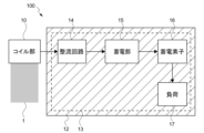
- FIG. 1 is a schematic diagram showing a configuration example of an energy harvester according to a first embodiment of the present technology.
- FIG. 2 is a block diagram showing a functional configuration example of the energy harvester 100.
- the energy harvester 100 is a device that extracts magnetic field energy generated around a metal body, a human body, or the like and harvests it as electric power. That is, it can be said that the energy harvester 100 is a device that performs environmental power generation using magnetic field energy in the surrounding environment.
- an object 1 a metal object or a human body from which magnetic field energy is extracted by the energy harvester 100 is referred to as an object 1 .
- the energy harvester 100 has a coil section 10, a housing 11, a non-magnetic material 12, and a circuit section 13. Further, as shown in FIG. 2 , circuit section 13 includes rectifier circuit 14 , power storage section 15 , power storage element 16 , and load 17 . At least the rectifier circuit 14 is provided in the circuit section 13 . Also, the power storage unit 15, the power storage element 16, and the load 17 may be provided separately from the circuit unit 13, for example, and may be connected as appropriate.
- the coil unit 10 is a coil that takes in magnetic field energy and outputs it as electric power.
- the coil portion 10 has a core 20 made of a magnetic material and a wire rod 21 wound around the core 20 .
- An axis O is set in the coil portion 10 .
- This axis O is the coil axis passing through the center of the loop formed by the wire rod 21 wound around the core 20 .
- the housing 11 is a case that accommodates the coil section 10 .
- the housing 11 functions as a member that holds the coil section 10 with respect to the target object 1 .
- the housing 11 holds the coil section 10 on the surface of the subject 1 such that the axis O of the coil section 10 intersects the surface of the subject 1 including a metal body or a human body.
- the magnetic field generated across the surface of the object 1 passes through the loop formed by the wire rod 21 of the coil section 10, and changes in the magnetic field can be reliably detected.
- the housing 11 corresponds to the holding section. The coil section 10 and the housing 11 will be described later in detail.
- the non-magnetic body 12 is a member made of a non-magnetic material, typically made of a non-magnetic metal.
- the non-magnetic body 12 is arranged at a predetermined distance from the coil section 10 .
- a plate-shaped member is used as the non-magnetic body 12 .
- the distance between the non-magnetic material 12 and the coil portion 10 is set, for example, within a range in which the coil portion 10 can exhibit the required characteristics. The relationship between the non-magnetic material 12 and the coil portion 10 will be described later in detail.
- the circuit unit 13 includes the rectifier circuit 14, the power storage unit 15, the power storage element 16, and the load 17 as described above. Also, the circuit section 13 is arranged on the opposite side of the coil section 10 with the non-magnetic material 12 interposed therebetween. As shown in FIG. 1, the circuit section 13 has a circuit board 40 on which a plurality of circuits such as the rectifier circuit 14 are formed. A non-magnetic material 12 is arranged between the circuit board 40 and the coil section 10 . More specifically, the circuit board 40 is connected to the surface of the non-magnetic body 12 opposite to the coil portion 10 . Note that in FIG. 2 , the non-magnetic material 12 is schematically illustrated as a hatched area surrounding each part of the circuit part 13 .
- the rectifier circuit 14 is a circuit that rectifies the output of the coil section 10 .
- the coil unit 10 outputs AC power in accordance with changes in magnetic flux.
- the rectifier circuit 14 rectifies AC power and converts it into DC power.
- the rectifier circuit 14 corresponds to a rectifier.
- the coil unit 10 and the rectifier circuit 14 constitute a power receiver that receives magnetic field energy generated around the object 1 as power.
- the power storage unit 15 is a circuit that charges the power storage element 16 .
- the power storage unit 15 charges the power storage element 16 with the power output from the rectifier circuit 14 .
- the power storage unit 15 outputs electric power necessary for charging, for example, according to the state of charge of the power storage element 16 .
- the electric power charged in the storage element 16 may be, for example, the output of the rectifier circuit 14 itself, or may be electric power stored in a capacitor or the like.
- the power storage element 16 is an element that stores power rectified by the rectifier circuit (power received by the coil section 10), and supplies the power to the load 17 as needed.
- a capacitor, a secondary battery, or the like, for example, is used as the storage element 16 .
- the energy harvester 100 functions as a charging device that charges the storage element 16 with the output of the coil section 10 via the rectifier circuit 14 and the storage section 15 .
- the load 17 is a circuit or element driven by the electric power of the storage element 16 .
- a control unit such as a microcomputer, a communication unit, various sensors, and the like are used as the load 17 .
- FIG. 3 is a schematic diagram for explaining the magnetic field generated in the object 1.
- the electric current 2 flowing through the object 1 is schematically illustrated by dotted arrows.
- the direction of the dotted arrow indicates the direction of the current.
- a magnetic field 3 generated by the current 2 is schematically illustrated by solid arrows.
- the direction of the solid arrow indicates the direction of the magnetic field 3 (magnetic flux).
- a magnetic field 3 corresponding to the current 2 is generated around the object 1 through which the current 2 flows.
- the direction of the magnetic field 3 is also reversed.
- a potential difference is basically generated with respect to the potential of the earth unless it is forcibly grounded to the earth GND (earth ground 4).
- most home electric appliances convert alternating current power into direct current power for use. For example, when converting power from alternating current to direct current, pulse signals with positive (+) and negative (-) potentials may be generated.
- home appliances use various clock frequencies for power conversion and the like, and the GND itself provided in the circuit of the home appliance may fluctuate. As a result, a potential difference is generated between the home appliance and the earth ground 4, and AC currents of various frequencies flow through the home appliance.
- the object 1 is floating from the earth ground 4 and an alternating current 2 is flowing.
- This can also be said to be a state in which a virtual AC power supply 5 is connected between the object 1 and the earth ground 4, as shown in FIG.
- a current 2 flowing through the object 1 is a current whose direction changes alternately.
- This current 2 is, for example, a product obtained by superimposing alternating currents of various frequencies.
- an upward magnetic field 3 is generated in the drawing.
- a downward magnetic field 3 is generated in the drawing.
- the direction of the current 2 changes again, and when the current 2 flows from the left side to the right side in the drawing as in #3, an upward magnetic field 3 is generated in the same manner as in the case of #1.
- an alternating magnetic field 3 is generated in a direction penetrating the surface of the object 1 due to the alternating current 2 flowing through the object 1 .
- the magnetic field 3 generated by the current 2 exhibits, for example, an annular distribution rotating around the current 2 . Therefore, depending on where the magnetic field 3 is generated, the relationship between the direction of the current 2 and the direction of the magnetic field 3 shown in FIG. 3 may be reversed.
- an alternating current 2 is induced in the object 1 and a magnetic field 3 is generated around the object 1 .
- the electric field acting on the object 1 includes electric fields of various frequencies, such as radio waves propagating around the object 1 and quasi-electrostatic fields generated around the object 1 . These electric fields can induce alternating currents 2 even in objects 1 that are not connected to an alternating current source, such as a human body or a metal shelf. In this case, a magnetic field 3 is generated around the object 1 according to the current 2 induced by the electric field.
- the object 1 may be, for example, an object in which an alternating current 2 is induced and a magnetic field 3 is generated.
- the object 1 includes a metal object or a human body.
- Metal objects are industrial products (cars, vending machines, refrigerators, microwave ovens, metal racks, guardrails, mailboxes, traffic lights, etc.) and objects made of metal. It is in a state of floating from the earth ground 4.
- the metal body may be made of any metal such as iron, aluminum, copper, metal alloy, etc., and the material is not limited as long as it is metal.
- the energy harvester 100 is configured for such magnetic field energy. The configuration of each part of the energy harvester 100 will be specifically described below.
- FIG. 4 is a schematic diagram showing a configuration example of the coil section 10. As shown in FIG. The coil portion 10 is configured by winding a wire rod 21 around a core 20 . Wire 21 may be directly wound around core 20 , or another member may be provided between core 20 and wire 21 . For example, when forming the housing 11 made of resin using a technique such as molding, it is possible to cover the entire core 20 with resin. In this case, wire rod 21 is wound around core 20 coated with resin.
- the core 20 of the coil section 10 is configured using a magnetic material.
- the core 20 with high magnetic permeability is arranged inside the coil, and the Q value of the coil is improved.
- the Q value of the coil is an index showing the relationship between energy retention and loss in the coil. For example, the higher the Q value, the smaller the energy loss. Therefore, by increasing the Q value of the coil section 10, it is possible to efficiently take in the magnetic field energy.
- the magnetic material forming core 20 is soft ferrite.
- Soft ferrite is an insulating ceramic with soft magnetic properties.
- Soft ferrite is characterized by a small coercive force that retains magnetic force and a high magnetic permeability. Therefore, when the external magnetic field disappears, the magnetic force disappears, but while the external magnetic field is acting, the magnetic flux density increases and it is strongly magnetized.
- Soft ferrite can also be magnetized in response to magnetic fields over a wide frequency range. Therefore, by using the core 20 made of soft ferrite, it is possible to efficiently capture magnetic field energy in a wide frequency range. This greatly improves the efficiency of capturing the magnetic field energy.
- the soft ferrite constituting the core 20 is made of a material having a high magnetic permeability at the frequency of the magnetic field to be taken in, for example. Therefore, the type of soft ferrite is selected according to the frequency of noise (AC current) to be received.
- AC current the frequency of noise
- Mn—Zn based soft ferrite is used for frequencies in the range of 50 Hz to several MHz.
- Ni—Zn soft ferrite is used.
- Mn--Zn soft ferrite having high magnetic permeability is used.
- Ni--Zn-based soft ferrite is used for the object 1 in which an alternating current of several MHz or more is induced.
- the wire material 21 of the coil part 10 is, for example, a litz wire that is formed into one electric wire by twisting a plurality of thin wires each of which is insulated.
- a specific configuration of the wire rod 21 is not limited, and for example, a single wire rod 21 may be used.
- the wire rod 21 is wound a predetermined number of turns around the core 20 (an axial core portion 23 to be described later).
- the winding method of the wire rod 21 is alpha winding. That is, the wire rod 21 becomes an alpha winding.
- Alpha winding is a winding method in which the wire rod 21 at the winding start and the winding end is wound around the outer circumference of the coil.
- an alpha winding is configured by winding both ends of the wire rod 21 outward at the same time. This prevents one end of the wire 21 from being left inside the winding, improves the space factor of the wire 21, and improves the coil performance such as the Q value.
- the method of winding the wire 21 is not limited to alpha winding, and other winding methods may be used.
- the core 20 is formed using a magnetic material (here, soft ferrite), and the litz wire is wound around the core 20 (axial core portion 23) by alpha winding to improve the Q value. ing. Both ends of the wire 21 are hereinafter referred to as a first coil terminal 21a and a second coil terminal 21b, respectively.
- FIG. 5 is a schematic diagram showing a configuration example of the core 20 of the coil section 10.
- the core 20 has a shaft portion 23 and a pair of flange portions 24 .
- the core portion 23 is a portion around which the wire rod 21 is wound, and is a solid member that fills the inside of the loop formed by the wire rod 21 .
- the axial core portion 23 has a columnar shape extending along the axis O of the coil portion 10, and the wire rod 21 is wound along the side surface thereof.
- a cylindrical shape, a polygonal prism shape such as a square prism shape, an elliptical shape, or the like is used.
- the pair of flange portions 24 are provided at both ends of the shaft core portion 23 and form flanges projecting outward from the side surfaces of the shaft core portion 23 . Therefore, the core 20 has a drum-shaped (H-shaped) shape in which the shaft core portion 23 is sandwiched between the pair of flange portions 24 .
- the planar shape of each flange portion 24 is, for example, a circular shape, a polygonal shape such as a quadrangle, an elliptical shape, or the like.
- the planar shape of the flange portion 24 may be a shape obtained by enlarging the cross-sectional shape of the axial core portion 23 or a shape matching the shape of the housing 11 or the like. Note that the flange portion 24 does not necessarily have to be provided, and for example, the core 20 may have a structure without the flange portion 24 .
- the housing 11 holds the coil part 10 so that one of the pair of flange parts 24 faces the target object 1 .
- the flange portion 24 directed toward the target object 1 is referred to as a first flange portion 24a
- the portion 24 is described as a second flange portion 24b.
- the lower flange portion 24 and the upper flange portion 24 in the drawing are referred to as a first flange portion 24a and a second flange portion 24b, respectively.
- the core 20 of the coil portion 10 also has a first end face 25a facing the target object 1 and a second end face 25b opposite to the first end face 25a.
- the surface of the first flange portion 24a opposite to the side connected to the axial core portion 23 serves as the first end surface 25a.
- the surface of the second flange portion 24b opposite to the side connected to the shaft core portion 23 serves as a second end surface 25b.
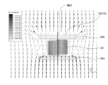
- FIG. 6 is data mapping the magnetic field passing through the drum-shaped core 20 .
- Arrows representing magnetic flux are mapped on a plane passing through the axis O of the coil section 10 .
- the direction of each arrow represents the direction of the magnetic field at each point, and the color of each arrow represents the strength (A/m) of the magnetic field at each point.
- a wire rod 21 is wound around the core 20 to form the coil portion 10 . It is also assumed that the axis O of the coil portion 10 is oriented in the vertical direction (Z direction) in the drawing, and that an external magnetic field is generated in the upward direction in the drawing. Therefore, the magnetic flux entering the core 20 from the lower first flange portion 24 a of the core 20 escapes from the upper second flange portion 24 b of the core 20 .
- the direction of the magnetic flux is bent so as to concentrate on the first flange portion 24a projecting outward from the axial core portion 23.
- the direction of the magnetic flux is bent so as to spread from the second flange portion 24b projecting outward from the axial core portion 23.
- the direction of the magnetic flux is bent so that the magnetic flux concentrates on the axial core portion 23 .
- the housing 11 has a first end 26a, a second end 26b and a side 27.
- the first end portion 26a and the second end portion 26b are plate-shaped members arranged perpendicular to the axis O of the coil portion 10 and facing each other.
- the side portion 27 is a plate-like member extending along the axis O of the coil portion 10 and connects the first end portion 26a and the second end portion 26b.
- a U-shaped housing 11 is configured in which a first end portion 26a and a second end portion 26b protrude in the same direction from both ends of a plate-shaped side portion 27. be.
- the housing 11 accommodates the coil section 10 .
- the housing 11 is configured such that at least part of the coil section 10 is accommodated inside the housing 11 or in the space formed by the housing 11 .
- the first flange portion 24a is embedded inside the first end portion 26a
- the second flange portion 24b is embedded inside the second end portion 26b.
- the axial core portion 23 around which the wire rod 21 is wound is arranged in the space sandwiched between the first end portion 26a and the second end portion 26b.
- the coil section 10 is accommodated in the gap formed in the U-shaped housing 11 .
- the housing 11 is made of, for example, a resin material such as plastic, and is formed using a technique such as molding. In this case, the housing 11 is formed by filling the resin material with the core 20 placed in the mold. Alternatively, the configuration may be such that the core 20 is fitted after the housing 11 is formed. Further, the configuration of the housing 11 is not limited to the example shown in FIG. For example, the housing 11 may be constructed so as to cover the entire core 20 including the axial core portion 23 . In this case, the wire rod 21 is wound around the resin material covering the shaft core portion 23 . Moreover, the housing 11 may be configured such that the core 20 around which the wire rod 21 is wound is covered with a resin material.
- the housing 11 is attached to the surface of the target object 1 . That is, the housing 11 is configured to be fixed in contact with or in close proximity to the surface of the target object 1 .
- a mounting surface 28 is the surface that contacts or approaches the surface of the target object 1 .
- the mounting surface 28 is the surface facing the outside of the plate-like first end portion 26 a (the side opposite to the second end portion 26 b ).
- the mounting surface 28 is basically a flat surface, but may have a curved shape such as a concave surface or a convex surface according to the shape of the surface of the object 1, for example.
- the housing 11 is provided with a mounting mechanism (not shown) for mounting on the surface of the target object 1 .
- a mounting mechanism (not shown) for mounting on the surface of the target object 1 .
- Bands, adhesive tapes, screwing mechanisms, magnets, clips, fitting grooves, suction cups, adhesives, etc. are used as mounting mechanisms.
- any fixture that can attach the housing 11 to the surface of the target object 1 may be used.
- the housing 11 is fixed with the mounting surface 28 in contact with the exterior of the home appliance or the like.
- the housing 11 is formed in a size that can be worn by a human body, and is fixed with the mounting surface 28 in contact with the skin of the human body or the surface of clothing.
- the housing 11 holds the coil section 10 so that the axis O of the coil section 10 and the mounting surface 28 are perpendicular to each other.
- the coil section 10 can be arranged with the axis O of the coil section 10 orthogonal to the surface of the target object 1 .
- the magnetic field created by the current flowing through the object 1 is orthogonal to the direction of current flow. Therefore, in the vicinity of the surface of the target object 1, a magnetic field is mainly generated in a direction orthogonal to the surface of the target object 1.
- FIG. Therefore, the direction in which the magnetic field changes is the direction perpendicular to the surface of the object 1 (normal direction to the surface of the object 1).
- the axis O of the coil section 10 is orthogonal to the surface of the target object 1, and the direction in which the magnetic field changes and the axis O of the coil section 10 are aligned. will match. This makes it possible to take in the magnetic field energy without waste.
- the housing 11 includes the coil section 10 so that the end surface (first end surface 25a) of the core 20 directed toward the target object 1 and the mounting surface 28 are aligned in the direction of the axis O of the coil section 10. may be retained. Therefore, the housing 11 may be configured such that the first end surface 25a of the first flange portion 24a is exposed and functions as the mounting surface 28 . Alternatively, a configuration may be adopted in which the first end surface 25a protrudes from the housing 11 toward the target object 1 side. As a result, the distance between the surface of the object 1 and the core 20 is close, and the magnetic field can be collected at a position where the magnetic field is strong (the magnetic flux density is large), and the magnetic field energy can be efficiently captured.
- the non-magnetic body 12 is a plate-like or sheet-like member arranged at a certain distance from the coil portion 10 . As shown in FIG. 1 , a side portion 27 of the housing 11 has a side surface 29 opposite to the coil portion 10 . The non-magnetic body 12 is fixed to the side surface 29 of this housing 11 .
- the method for fixing the non-magnetic body 12 to the side surface 29 is not limited, and methods such as adhesion, screwing, and fitting may be used. In this configuration, the distance between the side surface 29 of the housing 11 and the coil portion 10 (for example, the distance from the axis O of the coil portion 10 to the side surface 29) is the distance between the coil portion 10 and the non-magnetic material 12.
- the non-magnetic material 12 is capable of causing a magnetic field (magnetic flux) to flow at a position separated from the coil section 10 by a certain distance. As a result, the magnetic field around the coil section 10 is prevented from being absorbed by other metals included in the circuit section 13, and the effect of keeping the flow of the magnetic field properly is exhibited. In addition, since the non-magnetic material 12 has less loss of magnetic field energy due to eddy currents than ferromagnetic metal, it is possible to sufficiently suppress deterioration of the Q value. By covering the coil section 10 with the non-magnetic material 12 at a certain distance from the coil section 10 in this manner, the influence of the circuit section 13 can be reduced.
- the non-magnetic material 12 is configured so as to be able to cover the surface of the circuit board 40 to be described later facing the coil section 10 . Therefore, from the circuit board 40 side, the coil section 10 is completely blocked by the non-magnetic material 12 and cannot be seen.
- the non-magnetic body 12 is configured to have the same shape and size as the circuit board 40 .
- the non-magnetic body 12 may be configured to have a planar shape larger than that of the circuit board 40 . This makes it possible to sufficiently reduce the influence of the metal contained in the circuit board 40 (circuit section 13 ) on the coil section 10 .
- the non-magnetic body 12 is arranged parallel to the axis O of the coil portion 10 .
- the side surface 29 of the housing 11 is configured as a surface parallel to the axis O of the coil section 10
- the non-magnetic material 12 is arranged along the side surface 29 .
- the side surface 29 is inclined with respect to the axis O of the coil unit 10
- the magnetic field distributed along the axis O of the coil portion 10 can flow without significantly changing the direction of the magnetic field. It becomes possible to sufficiently suppress deterioration of the Q value of 10. Further, by setting the non-magnetic body 12 in a posture parallel to the axis O of the coil section 10, even if the non-magnetic body 12 is brought close to the coil section 10, the Q value and the like are hardly affected. This makes it possible to make the device size compact.
- Aluminum is typically used as the non-magnetic material 12 . This makes it possible to reduce the weight of the device. Copper may also be used as the non-magnetic material 12 . In addition, any non-magnetic metal may be used. Further, in this embodiment, a plate member having a thickness of 0.3 mm or more, for example, is used as the non-magnetic body 12 . A thickness of about 0.3 mm can sufficiently suppress deterioration of the Q value of the coil portion 10 . Of course, a non-magnetic material 12 with a thickness of 0.5 mm or 1 mm may be used. Also, a non-magnetic material 12 having a thickness of less than 0.3 mm may be used as long as the decrease in the Q value is within an allowable range.
- FIG. 7 is a graph showing the relationship between the distance between the plate (non-magnetic material 12) using a non-magnetic material metal and the coil portion 10 and the Q value.
- the horizontal axis of the graph is the distance between the metal and the side surface of the coil portion 10 .
- the vertical axis of the graph is the Q value of the coil section 10 .
- the data shown in FIG. 7 is obtained by measuring the Q value by changing the positions of the aluminum (Al) plate and the stainless steel (SUS) plate. The thickness of the measured plate was 0.5 mm in all cases, and measurements were made on plates of 7 mm x 20 mm and 90 mm x 30 mm for each material.
- the Q value of the coil portion 10 tends to deteriorate when there is a metal plate nearby, and the Q value deteriorates as the area of the metal plate increases.
- aluminum has less deterioration of the Q value than stainless steel. This is because a single non-magnetic material such as aluminum or copper does not accumulate magnetic lines of force in comparison to stainless steel, which is made mainly of iron, which is a magnetic material, so eddy currents are less likely to flow.
- stainless steel which is made mainly of iron, which is a magnetic material
- the distance between the non-magnetic body 12 and the coil portion 10 is set so that the deterioration of the Q value falls within an allowable range.
- the Q value of the coil section 10 can be measured using, for example, an LCR meter, a Q meter, or the like.
- the arrangement distance between the non-magnetic body 12 and the coil section 10 is, for example, a distance such that the Q value of the coil section 10 is 20% to 30% lower than the Q value when the non-magnetic body 12 is not arranged. is set to As a result, the device size can be made compact while maintaining a sufficient Q value. Further, for example, the distance may be set so that the amount of deterioration from the Q value when the non-magnetic material 12 is not arranged is 10% or less. This makes it possible to sufficiently improve the efficiency of capturing the magnetic field energy.
- the non-magnetic material 12 does not necessarily need to be provided.
- the circuit section 13 is provided separately from the housing 11 that accommodates the coil section 10, and there is no metal that blocks the magnetic field near the coil section 10, the non-magnetic material 12 may not be provided.
- the circuit section 13 has a flat circuit board 40 arranged along the non-magnetic body 12 .
- the circuit board 40 is made of glass epoxy or the like, and is a mounting board on which various circuits are provided. or placed in close proximity.
- the circuit board 40 includes a rectifier circuit 14, a power storage unit 15, and a power storage element 16 for operating the energy harvester 100, various sensors serving as a load 17, and BLE (Bluetooth (registered (trademark) Low Energy) and other communication devices are provided.
- BLE Bluetooth (registered (trademark) Low Energy)
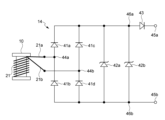
- FIG. 8 is a circuit diagram showing an example of a rectifier circuit.
- the rectifier circuit 14 is configured as a full-wave rectifier circuit.
- the rectifier circuit 14 has four diodes 41a to 41d, two Zener diodes 42a and 42b, an anti-backflow diode 43, and output terminals 45a and 45b.
- the diode 41a and the diode 41b are connected in series with the diode 41a leading in the forward direction.
- a connection point 44a is provided between the diode 41a and the diode 41b.
- the diode 41c and the diode 41d are connected in series with the diode 41c leading in the forward direction.
- a connection point 44b is provided between the diode 41c and the diode 41d.
- a cathode of each of the diode 41 a , the diode 41 c , the Zener diode 42 a and the Zener diode 42 b is connected to the anode of the backflow prevention diode 43 .
- a cathode of the backflow prevention diode 43 is connected to the output terminal 45a.
- Each anode of the diode 41b, the diode 41d, the Zener diode 42a, and the Zener diode 42b is connected to the output terminal 45b.
- a first coil terminal 21a of the coil section 10 is connected to a connection point 44a between the diodes 41a and 41b.
- a second coil terminal 21b of the coil section 10 is connected to a connection point 44b between the diodes 41c and 41d.
- the AC magnetic field detected by the coil section 10 is output from the first and second coil terminals 21a and 21b as AC power.
- This alternating current power is full-wave rectified by four diodes 41a to 41d and output as direct current power from output terminals 45a and 45b.
- the rectifier circuit 14 shown in FIG. 8 is configured using the minimum diodes 41a to 41d required for full-wave rectification. As a result, unnecessary leakage current is suppressed, and the efficiency of capturing magnetic field energy can be sufficiently improved.
- the Zener diode 42a is an element for releasing static electricity or the like applied to, for example, the first and second coil terminals 21a and 21b.
- the Zener diode 42a functions as an electrostatic protection component that releases static electricity.
- the Zener diode 42b is, for example, an element for protecting the subsequent IC circuit (power storage unit 15, etc.) connected to the output terminals 45a and 45b.
- the Zener diode 42b functions as a low resistance conductor. As a result, it becomes possible to avoid a situation in which the subsequent circuit is damaged.
- the backflow prevention diode 43 is a diode that prevents backflow of current. By providing the anti-backflow diode 43, it is possible to suppress the backflow of current when the voltage of the coil section 10 drops, and to stably operate the subsequent circuit.
- the configuration of the rectifier circuit 14 is not limited.
- a voltage doubler rectifier circuit that doubles the voltage using a capacitor, a quadruple voltage rectifier circuit, a rectifier circuit incorporating a Cockcroft-Walton circuit, or the like may be used.
- a half-wave rectifier circuit or the like may be used.
- the rectifier circuit 14 may be appropriately configured according to the power reception characteristics of the coil section 10, the characteristics of the elements and circuits used as the load 17, and the like.
- FIG. 9 is a table showing forward voltage Vf and reverse current Is of a rectifying diode.
- FIG. 10 is a graph of IV measurements for the rectifying diode shown in FIG. Silicon and germanium diodes were measured as a rectifying diode product number 1N60, and another product number ISS108 was evaluated using a germanium diode manufactured by a different manufacturer.
- curve (a) is the characteristic of 1N60 (silicon)
- curve (b) is the characteristic of 1N60 (germanium)
- curve (c) is the characteristic of ISS108 (germanium).
- the current that flows when a voltage is applied in the reverse direction of the diode is the reverse current Is.
- the measurement data in FIG. 9 are data when 10 V is applied in the reverse direction of the diode.
- the forward voltage Vf is the voltage when the forward current (1 mA) begins to flow through the diode.
- the diode 1N60 silicon
- the reverse current Is when the forward voltage Vf of the diode is applied in the reverse direction was evaluated. Considering that the reverse current Is shown in FIG. Yes, 1N60 (germanium) is 0.21 ⁇ A and ISS108 (germanium) is 0.5 ⁇ A.
- 1N60 (silicon) is 1/27778, 1N60 (germanium) is 1/4762, and ISS108 (germanium) is 1/2000. That is, the rectifying diodes (41a to 41d) used in the rectifying circuit 14 need to have a ratio of about 4700 times or more, preferably 10000 or more. As a result, of the three example diodes, 1N60 (silicon) has the most suitable characteristics.
- the reverse current Is when applied in the reverse direction is preferably small.
- 1N60 (germanium) is 1.43 M ⁇ and ISS108 (germanium) is 0.38 M ⁇ .
- the resistance value for preventing the current from flowing in the reverse direction is large. is required, preferably 10 M ⁇ or more.
- 1N60 (silicon) has the most suitable characteristics.
- FIG. 11 is a schematic diagram showing an example of use of the energy harvester.
- an energy harvester 100 is attached to the exterior of a target object 1, which is a refrigerator 1a, which is a home appliance.
- the exterior of the refrigerator 1a is configured using, for example, a metal plate or the like, and the energy harvester 100 is attached using a magnet or the like.
- the refrigerator 1a also includes a portion (for example, an exterior, a frame, etc.) that floats with respect to the ground GND (earth ground 4).
- GND earth ground 4
- an AC current is induced in the refrigerator 1a in accordance with a household AC power supply or the like, and an AC magnetic field is generated on the surface of the refrigerator 1a. This magnetic field is captured as power by the energy harvester 100 .
- the energy harvester 100 is attached to the legs (frames) of the target object 1, which is a steel rack 1b that is a metal object.
- the steel rack 1b is arranged on the carpet 38 and is in a state of floating from the earth ground 4.
- electric fields such as radio waves propagating around the steel rack 1b and power source noise act on the steel rack 1b to induce an alternating current, and an alternating magnetic field is generated on the surface of the steel rack 1b. This magnetic field is captured as power by the energy harvester 100 .
- the human body 1c is used as the target body 1, and the energy harvester 100 is attached to the wrist of the human body 1c using a band or the like.
- the human body 1 a is wearing shoes or the like, and is in a state of floating from the earth ground 4 .
- radio waves propagating around the human body 1a, an electric field generated by walking, and the like act on the human body 1a to induce an alternating current, and an alternating magnetic field is generated on the surface of the human body 1a. This magnetic field is captured as power by the energy harvester 100 .
- FIG. 12 is a diagram showing an example of the specific configuration and characteristics of the coil section.
- a coil portion 10 shown in FIG. 12 is a thin coil using a drum-shaped core 20 having a circular planar shape when viewed in the direction of the coil axis.
- a Mn--Zn based ferrite core is used to receive low frequency power.
- the overall height (outer width) h1 of the core 20 is 3.3 mm
- the thickness w1 of the first flange portion 24a and the thickness W2 of the second flange portion 24b are both 0.3 mm. 6 mm
- the height (inner width) of the core portion 23 around which the wire rod 21 is wound is 2.1 mm.
- the diameter d1 of the core 20 as a whole (the diameter of the first flange portion 24a and the second flange portion 24b) is 25 mm ⁇
- the diameter d2 of the axial core portion 23 is 19 mm ⁇ .
- a litz wire having a wire diameter of 0.65 mm was wound around the axial core portion 23 of the core 20 by alpha winding to form the coil portion 10 .
- the number of windings of the litz wire was 3 stages and 6 layers.
- FIG. 12B shows the characteristics of the coil section 10 shown in FIG. 12A.
- the coil part 10 is measured alone without providing the non-magnetic material 12 .
- An LCR meter was used for this measurement, the measurement frequency was 120 kHz, and the measurement current was 1 mA.
- the inductance Ls of the coil portion 10 was 29.5 ⁇ H and the Q value was 118.8.
- the equivalent series resistance Rs of the coil portion 10 was 0.186 ⁇ , and the DC resistance Rdc was 0.127 ⁇ .
- the inventor mounted the coil portion 10 shown in FIG. 12 on the exterior of the refrigerator 1 and conducted an experiment in which electric power was harvested using the rectifier circuit 14 shown in FIG.
- the secondary battery which is the storage element 16
- the secondary battery was connected between the output terminals 45a and 45b of the rectifier circuit 14, and the secondary battery was directly charged via the backflow prevention diode 43.
- FIG. During charging the voltage V1 between output terminals 45a and 45b was 2.300V.
- the output voltage V2 of the rectifier circuit 14 before passing through the backflow prevention diode 43 here, the voltage between the detection point 46a on the cathode side and the detection point 46b on the anode side of the Zener diode 42b
- the voltage drop due to the backflow prevention diode 43 is about 0.144V.
- FIG. 13 is a graph showing Vf-If characteristics of a backflow prevention diode.
- FIG. 13 shows the relationship between the forward voltage Vf and the forward current If of the backflow prevention diode 43 for each measurement temperature (100° C., 75° C., 50° C., 25° C., 0° C., ⁇ 25° C.). ing.
- the horizontal axis of the graph is the forward voltage Vf applied to the anti-backflow diode 43
- the vertical axis of the graph is the forward current If flowing through the anti-backflow diode 43 .
- the coil portion 10 is held with the axis O intersecting with the surface of the target object 1 including a metal object or a human body. Further, the output of the coil section 10 is rectified and used as electric power. A core 20 of the coil portion 10 is made of a magnetic material. Therefore, the magnetic flux generated around the object 1 can be collected. This makes it possible to efficiently take in the magnetic field energy generated in the surrounding environment.
- FIG. 14 is a perspective view showing a configuration example of the core of the coil portion according to the second embodiment.
- FIG. 15 is a schematic diagram showing a configuration example of an energy harvester on which the core 51 shown in FIG. 14 is mounted.
- the core 51 of the coil portion 50 is configured such that the periphery of the axial core portion 53 is covered with a magnetic material.
- the core 51 has a shaft portion 53 , a flange portion 54 and side wall portions 55 .
- the core 51 is entirely made of a magnetic material (typically soft ferrite).
- the shaft core portion 53 is a portion around which the wire rod 21 is wound, and is a solid member that fills the inside of the loop formed by the wire rod 21 .
- a cylindrical shaft core portion 53 is configured.
- the shape of the shaft core portion 53 is not limited, and any columnar shape may be used.
- the flange portion 54 is a portion that is provided at one end of the shaft core portion 53 and protrudes outward from the side surface of the shaft core portion 53 .
- the flange portion 54 having a square planar shape is formed, and the shaft core portion 53 is connected so that the central axis of the shaft core portion 53 (the axis O of the coil portion 50) passes through the center of the flange portion 54 .
- the planar shape of the flange portion 54 is not limited.
- the side wall portion 55 is a portion that is connected to the flange portion 54 and that surrounds at least a portion of the shaft core portion 53 while being spaced apart from the shaft core portion 53 . That is, the side wall portion 55 protrudes from the surface of the flange portion 54 to which the shaft core portion 53 is connected, and forms a wall surrounding the shaft core portion 53 at a position away from the shaft core portion 53 .
- the flange portion 54 having a square planar shape has side wall portions 55 protruding from three of the four sides forming the outer edge thereof. The distance between the axial core portion 53 and the side wall portion 55 is set so that the wire rod 21 can be wound at least a desired number of turns.
- FIG. 15A and 15B schematically show cross-sectional views of energy harvesters 200a and 200b configured using the core 51 shown in FIG.
- the circuit section 36 formed on the non-magnetic material 35 is directly arranged on the core 51 of the coil section 50.
- the present invention is not limited to this, and the coil section 50 (core 51) may be accommodated in a predetermined housing, and the non-magnetic material 35 and the circuit section 36 may be arranged on the housing.
- the energy harvesters 200a and 200b have the same configuration of the coil section 50 (core 51), but the positions of the non-magnetic material 35 and the circuit section 36 are different.
- the coil portion 50 is arranged such that the other end of the axial core portion 53 (the side opposite to the side where the flange portion 54 is provided) faces the target object 1 .
- the surface of the coil section 50 on the lower side in the drawing faces the target object 1 .
- the coil section 50 is directly held by using a predetermined mounting mechanism as a holding section so that the other end of the axial core section 53 faces the target object 1 .
- the coil portion 50 is accommodated in the housing, the coil portion 50 is held by using the housing as a holding portion so that the other end of the axial core portion 53 faces the target object 1 .
- the surface formed at the other end of the shaft core portion 53 is the first end face 56 a facing the target object 1 , and the side of the flange portion 54 connected to the shaft core portion 53 . is the second end face 56b.
- the shaft core portion 53 surrounded by the side wall portion 55 is exposed, and magnetic flux is easily taken in.
- magnetic flux tends to pass through the interior of magnetic materials. Therefore, by surrounding the axial core portion 53 with the side wall portion 55 and the flange portion 54 made of a magnetic material and directing the first end surface 56a side where the axial core portion 53 is exposed toward the target object 1, The effect of confining the generated magnetic flux is expected.
- This can be said to be a configuration in which the magnetic flux emitted from the target object 1 is limited only to the front side (first end face 56a side) that receives energy.
- the magnetic flux is concentrated on the shaft core portion 53 around which the wire 21 is wound, and the magnetic field energy can be taken in very efficiently.
- the non-magnetic material 35 and the circuit section 36 are arranged in this order on the second end surface 56b of the flange portion 54 opposite to the first end surface 56a. That is, the non-magnetic material 35 and the circuit section 36 are arranged perpendicular to the axis O of the coil section 50 .
- the side wall portion 55 as described above, the magnetic flux is less likely to leak, and even when the circuit portion 36 and the like are arranged on the axis O of the coil portion 50, the Q value is not significantly degraded.
- the non-magnetic material 35 and the circuit portion 36 are arranged in this order on the outer surface 57 of the side wall portion 55 . That is, the non-magnetic material 35 and the circuit section 36 are arranged perpendicular to the axis O of the coil section 50 .
- the non-magnetic material 35 and the circuit portion 36 are provided on the outer surface 57 of the central side wall portion 55 formed in a U shape, but the outer surfaces of the side wall portions 55 formed along the other two sides 57. In this case as well, since the magnetic flux is less likely to leak due to the flange portion 54 and the side wall portion 55, deterioration of the Q value due to the circuit portion 36 can be sufficiently suppressed. Further, in FIG.
- the contact surface that contacts the object 1 may be reversed. That is, the energy harvester 200b may be arranged such that the second end face 56b of the flange portion 54 contacts the surface of the target object 1.
- FIG. in this case, for example, magnetic flux can be collected from a wide range with which the flange portion 54 contacts.
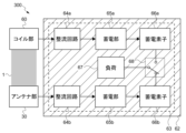
- FIG. 16 is a schematic diagram showing a configuration example of an energy harvester according to the third embodiment.
- FIG. 17 is a block diagram showing a functional configuration example of the energy harvester 300.
- the energy harvester 300 has a configuration in which an antenna section 30 for capturing electric field energy generated in the surrounding environment is provided in addition to the coil section 60 for capturing magnetic field energy.
- the energy harvester 300 has a coil section 60 , a housing 61 , a non-magnetic body 62 , a circuit section 63 and an antenna section 30 .
- the coil section 60, the housing 61, and the non-magnetic body 62 are configured in the same manner as the coil section 10, the housing 11, and the non-magnetic body 12 of the energy harvester 100 shown in FIG. 1, for example. Therefore, the energy harvester 300 shown in FIG. 16 is a device obtained by adding the antenna section 30 to the energy harvester 100 shown in FIG. 1 and changing the circuit configuration.
- the antenna unit 30 functions as a receiving antenna for receiving power through the object 1 including a metal object or a human body.
- the antenna unit 30 receives electric field energy of radio waves and quasi-electrostatic fields in the space around the object 1 as power. Therefore, the energy harvester 300 is a device capable of extracting magnetic field energy using the coil section 60 and extracting electric field energy using the antenna section 30 from the target object 1 such as a metal body or a human body. As a result, since power can be harvested from both the coil section 60 and the antenna section 30, energy can be efficiently harvested.
- the circuit section 63 of the energy harvester 300 has a circuit for the coil section 60 and a circuit for the antenna section 30 .
- a circuit for the coil unit 60 includes a rectifier circuit 64a, a power storage unit 65a, and a power storage element 66a.
- the circuit for the antenna section 30 includes a rectifier circuit 64b, a power storage section 65b, and a power storage element 66b.
- the circuit section 63 further has a switch section 68 and a load 67 .
- the circuitry for coil portion 60 charges the magnetic field energy captured by coil portion 60 .
- the rectifier circuit 64 a rectifies the output of the coil section 60 .
- the coil unit 60 and the rectifier circuit 64a constitute a power receiver that receives the magnetic field energy generated around the object 1 as power.
- the power storage unit 65a charges the power storage element 66a with the power output from the rectifier circuit 64a.
- the power storage element 66a is an element that stores power received by the coil section 60 .
- a charging device for the coil unit 60 is configured to charge the power storage element 66a with the output of the coil unit 60 via the rectifier circuit 64a and the power storage unit 65a.
- a circuit for the antenna section 30 charges the electric field energy captured by the antenna section 30 .
- the rectifier circuit 64 b rectifies the output of the antenna section 30 .
- the antenna unit 30 and the rectifier circuit 64b constitute a power receiver that receives electric field energy generated around the object 1 as power.
- the power storage unit 65b charges the power storage element 66b with the power output from the rectifier circuit 64b.
- the storage element 66b is an element that stores power received by the antenna section 30 .
- a charging device for the antenna section 30 is configured to charge the power storage element 66b with the output of the antenna section 30 via the rectifier circuit 64b and the power storage section 65b.
- the rectifier circuits 64a and 64b are configured similarly to the rectifier circuit 14 described with reference to FIG. 6, for example. 1, and storage elements 66a and 66b are configured, for example, similarly to the storage element 16 in FIG.
- a circuit corresponding to the characteristics of the coil section 60 and the antenna section 30 may be used.
- the rectifier circuit 64a corresponds to a coil rectifier circuit
- the rectifier circuit 64b corresponds to an antenna rectifier circuit.
- a rectifying section is configured by the rectifying circuit 64a and the rectifying circuit 64b.
- the switch unit 68 is a circuit that switches between the power storage element 66 a and the power storage element 66 b to connect to the load 67 .
- the load 67 is a circuit or element such as a sensor driven by the electric power of the storage elements 66a and 66b.
- the switch unit 68 detects, for example, the charging rates of the storage element 66 a and the storage element 66 b and performs control such that the one with the higher charging rate is connected to the load 67 .
- control may be performed to switch the connection of the load to the other storage element.
- the method for switching between the storage element 66a and the storage element 66b is not limited.
- the energy harvested from both the coil section 60 and the antenna section 30 is individually stored in the two storage elements 66a and 66b.
- the stored electric power is switched by the switch unit 68 and supplied to the load 67 .
- the energy harvested by the coil section 60 is magnetic field energy and the energy harvested by the antenna section 30 is electric field energy. Therefore, for example, the current generated in the coil section 60 and the current generated in the antenna section 30 may be out of phase by 90 degrees. Even in such a case, power can be stored without interference in this configuration. As a result, loss during conversion into electric power is reduced, and magnetic field energy and electric field energy can be taken in efficiently.
- FIG. 18 is a schematic diagram for explaining the operation of the antenna section 30.
- the antenna section 30 is provided with a first antenna conductor 31 and a second antenna conductor 32 .
- the first antenna conductor 31 is a conductor electrically coupled to the object 1 including a metal object or a human body.
- the second antenna conductor 32 is a conductor different from the first antenna conductor 31 and is a conductor that is not connected to the object 1 .
- FIG. 18 schematically illustrates how the first antenna conductor 31 is electrically coupled to the surface of the object 1 .
- the first antenna conductor 31 may be in direct contact with the surface of the object 1 or may be capacitively coupled.
- the antenna section 30 is a dipole antenna having a first antenna conductor 31 and a second antenna conductor 32 .
- an antenna with a dipole structure is an antenna that uses two antenna elements (also referred to as antenna elements) to transmit and receive an electric field.
- the target object 1 to which the first antenna conductor 31 is coupled is a metal object or a human body that is insulated (in a floating state) from the ground GND. Therefore, the object 1 functions as a one-sided antenna element via the first antenna conductor 31 . From another point of view, it can be said that the first antenna conductor 31 is an electrode for causing the object 1 to function as an antenna element. Since the second antenna conductor 32 is a conductor different from the first antenna conductor 31 and is not connected to the object 1, it functions as another antenna element.
- the antenna section 30 uses this effect to receive the energy of the electric field.
- various electric field energies exist in the environment in which humans are active. These electric field energies can be divided into low frequency components and high frequency components. For example, electric fields (50 Hz/60 Hz) leaked from AC power supplies in homes, noise near personal computers, and voltages generated when people walk are low-frequency components of electric field energy, and are called quasi-electrostatic fields (near-fields). ).
- radio broadcasting AM/FM
- television broadcasting communication radio waves of mobile phones, etc. are electric field energy of high frequency components, and are called radio waves (far field).
- the antenna unit 30 can take in electric field energy of both a quasi-electrostatic field such as noise, which is leakage current, and radio waves such as broadcast waves, using the target object 1 as an antenna element. Also, the antenna unit 30 receives power in which quasi-electrostatic field energy and radio wave energy are combined.
- FIG. 18 schematically shows the waveform of the power received via the object 1. As shown in FIG. The power waveform is a waveform containing a wide range of frequency components. By making the object 1 function as an antenna element in this way, it is possible to take in electric field energy over a very wide band.
- FIG. 16 The configuration of the antenna section 30 provided in the energy harvester 300 will be described below with reference to FIG. 16 .
- a first antenna conductor 31 electrically coupled to the object 1 and a second antenna conductor 32 provided separately from the first antenna conductor 31 are schematically illustrated as shaded areas. Illustrated.
- an alternating current flows between the first antenna conductor 31 and the second antenna conductor 32 according to the electric field around the object 1 .
- This can also be said to be a state in which a virtual AC power supply 5 is connected between the first antenna conductor 31 and the second antenna conductor 32, as shown in FIG.
- the first antenna conductor 31 is arranged on the surface of the target object 1 outside the area facing the coil portion 60 . That is, the first antenna conductor 31 is arranged to avoid the space between the coil portion 60 and the object 1 .
- a non-magnetic material 62 is arranged in parallel with the axis O of the coil portion 60 with a certain distance from the coil portion 60 .
- the first antenna conductor 31 is arranged along the surface of the object 1 opposite to the coil portion 60 with the non-magnetic body 62 interposed therebetween.
- the first antenna conductor 31 may be configured as a separate member, for example, and may be connected to the main body by wiring, or may be fixed to the housing 61 or the like using a holder such as a hinge.
- the Q value and the like of the coil portion 60 can be reduced. Sufficient suppression is possible.
- the presence of the non-magnetic material 62 between the coil portion 60 and the first antenna conductor 31 makes it possible to sufficiently suppress the influence of the first antenna conductor 31 on the coil portion 60 .
- the coil section 60 can be arranged close to the surface of the target object 1, so that magnetic field energy can be efficiently captured. Become.
- the first antenna conductor 31 a plate member made of a conductor such as gold, silver, aluminum, copper, iron, nickel, or an alloy is used. Also, the first antenna conductor 31 may have a linear shape, a pin shape, a hemispherical shape, or an uneven shape in accordance with the shape of the surface of the object 1 . As a result, the adhesion to the object 1 is improved, and power can be efficiently taken in. Further, the contact surface of the first antenna conductor 31 with the target object 1 may be resin-coated. This makes it possible to suppress corrosion or the like of the first antenna conductor 31 . As the first antenna conductor 31, for example, conductive resin or conductive rubber containing carbon or metal may be used.
- the material of the first antenna conductor 31 is not limited, and the above materials may be used alone, or the electrodes may be formed by combining the materials.
- the second antenna conductor 32 is arranged parallel to the axis O of the coil portion 60 . That is, the second antenna conductor 32 extends along the axis O of the coil portion 60 .
- a side surface 69 parallel to the axis O of the coil section 60 is formed in the housing 61 that houses the coil section 60 .
- a non-magnetic material 62 and a circuit board 70 forming a circuit portion 63 are arranged along the side surface 69 .
- a second antenna conductor 32 is formed on the circuit board 70 .
- the second antenna conductor 32 may be configured as a separate element on the circuit board 70, or may use the GND of the circuit that configures the circuit board 70. FIG. This makes it possible to easily realize the second antenna conductor 32 parallel to the axis O of the coil portion 60 .
- the conductor is arranged along the magnetic flux passing through the coil portion 60, and the coil portion by the second antenna conductor 32 It can be said that this arrangement suppresses the influence on 60 .
- the nonmagnetic material 62 is provided between the circuit board 70 on which the second antenna conductor 32 is provided and the coil section 60, the influence on the coil section 60 can be sufficiently suppressed. As a result, electric field energy can be taken in without lowering the magnetic field energy taking efficiency.
- FIG. 19 is a schematic diagram showing a configuration example of the second antenna conductor 32 formed on the circuit board 70.
- a circuit board 70 is provided with a board ground 71 and a conductor pattern 72 different from the board ground 71 .
- the board ground 71 is a pattern that serves as the ground for the circuit section 63 .
- the conductor pattern 72 is a pattern that becomes the second antenna conductor 32 and becomes an antenna element capacitively coupled with the earth ground 4 .
- the board ground 71 and the conductor pattern 72 are formed so as not to overlap the circuit section 63 .
- the circuit diagram of the rectifier circuit 64b for the antenna section 30 in the circuit section 63 is shown in the area surrounded by the board ground 71 and the conductor pattern 72. As shown in FIG.
- the configuration of the rectifier circuit 64b is similar to that of the rectifier circuit 14 described with reference to FIG.
- other circuits and elements such as the rectifier circuit 64a for the coil section 60 constituting the circuit section 63 shown in FIG. 17 may be provided.
- the first antenna conductor 31 is connected to the connection point 44a of the rectifier circuit 64b.
- the conductor pattern 72 which is the second antenna conductor 32, is connected to the connection point 44b of the rectifier circuit 64b.
- AC power corresponding to the electric field generated around the object 1 is supplied to the rectifier circuit 64b.
- the substrate ground 71 is grounded to the earth ground 4 via an insulated covered cable 75. In the example shown in FIG. This makes it possible to provide a stable ground potential to the circuit section 63 .
- a varistor 76 is inserted as an electrostatic protection component. The varistor 76 may be inserted between the output terminal 45a of the rectifier circuit 64b and the substrate ground 71.
- the conductor pattern 72 shown in FIG. 19 may be grounded to earth ground through an insulated jacketed cable.
- an electrostatic protection component such as a varistor
- grounding the conductor pattern 72 in this way it is possible to improve the efficiency of taking in electric power compared to the case of capacitive coupling with the earth ground 4, for example.
- the substrate ground 71 may be used as the second antenna conductor 32 .
- the substrate ground 71 is connected to the connection point 44b of the rectifier circuit 64b.
- the conductor pattern 72 is not required.
- the substrate ground 71 as the second antenna conductor 32 may be grounded to the earth ground 4 .
- a component having high impedance in the frequency band used may be required, so an inductor or the like may be inserted between the board ground 71 and the earth ground 4, for example.
- a static electricity protection component (varistor, etc.) is inserted between the substrate ground 71 and the first antenna conductor 31 (the connection point 44a of the rectifier circuit 64b).
- the substrate ground 71 may be capacitively coupled to the earth ground 4 without being grounded to the earth ground 4 .
- the second antenna conductor 32 in the circuit board 70 .
- a portion that does not come into contact with the target object 1 is configured using a conductor such as metal.
- a conductor portion of such a housing 61 may be used as the second antenna conductor 32 .
- a conductor portion of the housing 61 and the conductor pattern 72 connected by a cable may be used as the second antenna conductor 32, or a conductor portion of the housing 61 and the board ground 71 are connected by a cable. may be used as the second antenna conductor 32 .
- the non-magnetic material 62 provided in the housing 61 may be used as the second antenna conductor 32 .
- an insulated covered cable or the like is connected to the non-magnetic body 62 made of aluminum or copper by soldering, brazing, caulking, screwing, or the like. This cable is connected to the connection point 44b of the rectifier circuit 64b formed on the circuit board 70. FIG. This makes it possible to provide the second antenna conductor 32 without increasing the number of parts.
- FIG. 20 is a schematic diagram showing a configuration example of an energy harvester according to the fourth embodiment.
- the energy harvester 400 is configured by stacking an antenna section 90, which is an electric field antenna, and a coil section 80, which is a magnetic field antenna. With this configuration, it is possible to downsize the energy harvester 400 as a whole.
- Energy harvester 400 has coil section 80 , housing 81 , nonmagnetic material 82 , circuit section 83 , and antenna section 90 .
- the coil portion 80 and the housing 81 are configured in the same manner as the coil portion 10 and the housing 11 of the energy harvester 100 shown in FIG. 1, for example.
- the functional configuration of the circuit section 83 is similar to that of the circuit section 63 described with reference to FIG. 17, for example.
- the non-magnetic body 82 and the circuit section 83 are provided on the side of the coil section 80 opposite to the object 1 .
- the coil portion 80 is formed with a first end face 85a facing the target object 1 and a second end face 85b on the opposite side.
- the non-magnetic body 82 and the circuit portion 83 are arranged orthogonally to the axis O of the coil portion 80 on the second end surface 85b side. More specifically, the non-magnetic material 82 and the circuit section 83 are laminated in this order on the surface of the housing 81 on the side of the second end face 85a of the coil section 80 .
- the first antenna conductor 91 and the second antenna conductor 92 that constitute the antenna section 90 are arranged so as to sandwich the coil section 80 therebetween. Specifically, the first antenna conductor 91 is arranged to face the first end face 85 a of the coil portion 80 . Also, the second antenna conductor 92 is arranged to face the second end face 85b of the coil portion 80 .
- the first antenna conductor 91 is connected to the surface of the housing 81 on the side of the first end surface 85a of the coil section 80.
- the housing 81 and the coil section 80 are configured on the first antenna conductor 91 that is used in contact with the target object 1 such as a metal object or a human body.
- the device can be made smaller than, for example, the configuration in which the first antenna conductor 91 is arranged to avoid the space between the coil section 80 and the object 1 (see FIG. 16).
- the second antenna conductor 92 is arranged along the surface of the housing 81 on the side of the second end surface 85b of the coil section 80 .
- the second antenna conductor 92 is formed on the circuit portion 83 provided on the second end surface 85b side perpendicular to the axis O of the coil portion 80.
- the conductor pattern or the like described with reference to FIG. 19 is used as the second antenna conductor 92. In this way, by arranging the first antenna conductor 91 and the second antenna conductor 92 facing each other with the coil portion 80 interposed therebetween, it is possible to improve, for example, the amount of current induced in each conductor. .
- the device size can be reduced and the influence of the circuit part 83 and the like on the coil part 80 can be sufficiently reduced. can be suppressed to
- the second antenna conductor 92 may be configured using a conductor plate separate from the circuit section 83, a part of the housing 81, or the like. may Alternatively, the second antenna conductor 92 may be constructed using the non-magnetic material 82 . Also, the non-magnetic body 82 , the circuit portion 83 , and the second antenna conductor 92 may be arranged parallel to the axis O of the coil portion 80 . For example, a configuration is possible in which the non-magnetic material 82 , the circuit section 83 and the second antenna conductor 92 are arranged on the side surface 86 of the housing 81 .
- FIG. 21 is a block diagram showing a functional configuration example of the energy harvester according to the fifth embodiment.
- the energy harvester 500 has a coil section 110 , a housing (not shown), a non-magnetic body 112 , a circuit section 113 and an antenna section 120 .
- the circuit section 113 is formed with a shared circuit for charging the power output from the coil section 110 and the antenna section 120 .
- circuit section 113 includes rectifier circuit 114 , power storage section 115 , power storage element 116 , and load 117 .
- the rectifier circuit 114 is connected to both the coil section 110 and the antenna section 120 and rectifies the output of the coil section 110 and the output of the antenna section 120 .
- the rectifier circuit 114 corresponds to a shared rectifier circuit.
- the rectifier circuit 114 is configured in the same manner as the rectifier circuit 14 described with reference to FIG. 8, for example.
- the output of the coil section 110 and the output of the antenna section 120 rectified by the rectifying circuit 114 are stored in the storage element 116 via the storage section 115 and supplied appropriately to the load 117 in the subsequent stage.
- FIG. 22 is a circuit diagram showing an example of connection of the coil section 110 and the antenna section 120 to the rectifier circuit 114.
- the first coil terminal 21 a of the coil section 110 is connected to the connection point 44 a of the rectifier circuit 114 via the first antenna conductor 121 of the antenna section 120 .
- Second coil terminal 21 b of coil section 110 is connected to connection point 44 b of rectifier circuit 114 via second antenna conductor 122 of antenna section 120 . This makes it possible to supply the outputs of both the coil section 110 and the antenna section 120 to the rectifier circuit 114 .
- the outputs of the coil section 60 which is a magnetic field antenna
- the output of the antenna section 30, which is an antenna for an electric field are separately charged to storage elements such as batteries, and then switched for use. It was something.
- This configuration takes into consideration that the phases of the magnetic field and the electric field are out of phase by 90°. In this case, it is necessary to provide a dedicated circuit for each antenna.
- the outputs of the coil section 110 and the antenna section 120 can be stored using a shared circuit. It is considered that the magnetic field and electric field generated around the object 1 contain various frequency components. Therefore, depending on the environment in which the energy harvester 500 is used, it may receive magnetic field energy and electric field energy of various frequencies. Furthermore, it takes a certain amount of time from when the energy is taken in to when the power is supplied. For example, the time required for power supply may vary from frequency to frequency or antenna to antenna. For these reasons, the power output from the coil section 110 and the power output from the antenna section 120 are not necessarily out of phase by 90°. Therefore, it is possible to connect the outputs from the coil section 110 and the antenna section 120 in series or in parallel as in the present embodiment. This eliminates the need to provide a dedicated circuit for each antenna, making it possible to reduce the cost of the device.
- the core of the coil portion is mainly made of a single magnetic material (soft ferrite).
- the core is not limited to this, and the core may be configured by combining two or more magnetic materials.
- an amorphous alloy with high magnetic permeability may be applied to the two flange portions of a drum-shaped (H-shaped) core.
- Amorphous alloys include, for example, cobalt (Co)-based amorphous alloys such as Mg--Zn alloys.
- Co cobalt
- Mg--Zn alloys cobalt-based amorphous alloys
- the entire core can be made smaller.
- the entire core may be made of an amorphous alloy.
- a core such as the type I used may be used.
- the coil part it is not necessary to arrange the coil part so that the axis of the coil part is orthogonal to the surface of the object.
- the axis of the coil section may be inclined with respect to the surface of the object. Even in this case, it is possible to capture the magnetic flux extending from the surface of the object and take it in as electric power.
- the coil part may be arranged so as to take a posture that can efficiently collect the magnetic flux according to the spatial distribution of the current in the target object (such as the three-dimensional shape of the exterior).
- the coil portion does not necessarily have to be attached to the surface of the object.
- a holding mechanism such as a clamp that is provided outside the object and holds the coil portion may be used. With such an external holding mechanism, electric power can be taken in by placing the coil portion in contact with or in close proximity to a target object such as a home appliance.
- the circuit section need not be provided on the coil section or its housing, and the circuit section and the coil section may be configured separately. Moreover, there may be a form in which a plurality of coil units are connected to one circuit unit. Alternatively, a receiving unit or the like may be configured in which a coil section for capturing magnetic field energy and an antenna section for capturing electric field energy are unitized. In this case, the receiving unit may be connected to the circuit section by predetermined wiring. Also, a plurality of receiving units may be connected to one circuit section.
- FIG. 23 is a circuit diagram showing a configuration example of an energy harvester equipped with a separating section.
- An energy harvester 601 shown in FIG. 23 is mounted inside a device and harvests electric field energy generated from the device as electric power.
- Energy harvester 601 has antenna section 130 , circuit section 140 , and separation section 150 .
- the energy harvester 601 is provided with a coil section together with the antenna section 130 .
- a circuit for charging power from the antenna section 130 and a circuit for charging power from the coil section may be provided independently.
- a shared circuit for charging power from the antenna section 130 and the coil section may be provided. Note that the configuration described below may be applied to an energy harvester provided with only the antenna section 130 as an electric field antenna without providing a coil section as a magnetic field antenna.
- the antenna section 130 has two antenna elements (a first antenna element 131 and a second antenna element 132) for capturing electric field energy.
- Devices on which the energy harvester 601 is mounted include conductors such as GND for various substrates and metal cases. These conductors are used as the first antenna element 131 and the second antenna element 132 . This eliminates the need to newly add a conductor that serves as an antenna element, so the energy harvester 601 can be easily mounted on various devices. Conductors used as the first antenna element 131 and the second antenna element 132 will be described later.
- the circuit unit 140 is a circuit that uses power output from the antenna unit 130 to charge a storage element (not shown).
- FIG. 23 shows a rectifier circuit 141 that rectifies the output from the antenna section 130 in the circuit section 140 .
- the rectifier circuit 141 is configured in the same manner as the rectifier circuit 14 described with reference to FIG. 8, for example.
- the first antenna element 131 is connected to the connection point 44 a of the rectifier circuit 141 and the second antenna element 132 is connected to the connection point 44 b of the rectifier circuit 141 .
- a power storage unit, a power storage element, and the like are provided after the rectifier circuit 141 . Note that the configuration of the rectifier circuit 141 and the like that constitute the circuit unit 140 is not limited.
- the separation section 150 is provided between the first antenna element 131 and the second antenna element 132, and separates the first antenna element 131 and the second antenna element 132 so that electric field energy does not leak. Specifically, the separation unit 150 makes it difficult for an AC component having electric field energy to flow between the first antenna element 131 and the second antenna element 132, that is, suppresses passage of the AC component.
- a separation resistor 151 is provided as the separation section 150 .
- the isolation resistor 151 is an element such as a wire-wound resistor set with a predetermined DC resistance value.
- the energy harvester 601 is mounted on equipment that is not grounded, for example.
- a device that does not need to be grounded is, for example, a device that is used by being connected to an AC power supply but does not need to be grounded. Examples of such devices include products such as televisions, hard disk recorders, game machines, and audio components. Also, for example, drones, automobiles, and the like operate in a state of having a constant resistance with the earth ground. These devices can be said to be devices that are used in a state that they are not grounded to the earth ground, that is, they are used in a state that they are electrically floating from the earth ground.
- a GND (hereinafter referred to as a power GND 135) of a power supply board including a converter circuit, an inverter circuit, etc. that generate a large amount of power, and a power supply GND 135 provided in the device
- a power GND 135 provided in the device
- the conductor portion such as the metal portion (hereinafter referred to as another conductor 136)
- the power supply GND 135 and the other conductor 136 as antenna elements and separating each antenna element, it is possible to efficiently take in the electric field energy generated from the converter circuit, the inverter circuit, and the like.
- the power supply GND 135 of the equipment on which the energy harvester 601 is mounted is used as the first antenna element 131 .
- conductor 136 other than power supply GND 135 is used as second antenna element 132 .
- the other conductor 136 is, for example, a radiator plate provided in the device, a metal case, or the like.
- any conductor provided separately from the power supply GND 135 may be used as the second antenna element 132 without being limited to this.
- a power supply GND 135 that is the first antenna element 131 and another conductor 136 that is the second antenna element 132 are separated by a separation resistor 151 that is used as a separation section 150 .
- the power supply GND 135, which is the first antenna element 131 is not grounded to the earth ground, so it becomes a conductor floating from the earth ground.
- the other conductor 136 which is the second antenna element 132, may not be grounded to the earth, or may be grounded to the earth. That is, the power supply GND 135 and the other conductor 136 are separated by the separation resistor 151, and the power supply GND 135 is floating from the earth ground.
- Other conductors 136 function as separate antenna elements.
- the energy harvester 601 can be applied to equipment in which at least the power supply GND 135 is not connected to the earth ground.
- the isolation resistor 151 By providing the isolation resistor 151, it becomes difficult for AC components to flow between the power supply GND 135, which is the first antenna element 131, and the other conductor 136, which is the second antenna element 132. Therefore, the power GND 135 and the other conductor 136 act as a dipole antenna. As a result, an AC component is induced between the power supply GND 135 and another conductor 136 according to the electric field generated by the inverter circuit or the like provided on the power supply board, and the power can be harvested.
- the inventor conducted an experiment to measure the power output from the antenna section 130 (the first antenna element 131 and the second antenna element 132) by changing the resistance value of the isolation resistor 151.
- FIG. From this experimental result, if the resistance value of the isolation resistor 151 is 10 k ⁇ or more, the first antenna element 131 and the second antenna element 132 are sufficiently isolated, and electric power is generated that can be used for charging. I found out to do. That is, by inserting a separation resistor 151 of 10 k ⁇ or more between the first antenna element 131 and the second antenna element 132, power can be harvested from the energy harvester 601.
- the resistance value of the isolation resistor 151 is preferably 10 k ⁇ or more. Note that the resistance value of the separation resistor 151 is not limited to this, and a separation resistor 151 having a resistance value of 10 k ⁇ or less may be used depending on the application of the energy harvester 601, for example.
- the GND (power GND 135) of the power supply board including the inverter circuit etc. is connected to another metal part (other conductor 136) such as a metal case provided in the device so that the resistance is substantially zero.
- another metal part such as a metal case provided in the device so that the resistance is substantially zero.
- the power supply GND 135 and the other conductor 136 function as one conductor, it becomes difficult to use each as an antenna element.
- the power supply GND 135 and the other conductor 136 are separated by the separation resistor 151, so that the power supply GND 135 functions as the first antenna element 131 and the other conductor 136 functions as the second antenna element. 132.
- the separation resistor 151 By separating the conductors inside the device in advance in this way, it is possible to harvest a larger amount of power than, for example, when an energy harvester is provided outside the device and connected to the device for use.
- FIG. 24 is a circuit diagram showing another configuration example of an energy harvester having a separation section.
- the energy harvester 602 shown in FIG. 24 is provided with a filter section 152 as the separating section 150 . It should be noted that the energy harvester 602 is used by being mounted on a device that is not connected to the earth ground, like the energy harvester 601 shown in FIG.
- the filter unit 152 is configured to connect the first antenna element 131 and the second antenna element 132 with a relatively low DC resistance while suppressing passage of an AC component having a specific frequency.
- the specific frequency is, for example, the frequency of the electric field energy to be harvested by the energy harvester 602 .
- the filter unit 152 for example, an element or circuit is used that has a low DC resistance for a DC component and a high impedance for an AC component having a specific frequency.
- the filter section 152 By using the filter section 152, it becomes difficult for AC components to flow between the power supply GND 135, which is the first antenna element 131, and the other conductor 136, which is the second antenna element 132, and the antenna section 130 has a dipole structure. function as an antenna for Furthermore, by using the filter section 152, the power supply GND 135 and another conductor 136 are connected via a low DC resistance. As a result, the other conductor 136 also functions as part of the power supply GND 135, making it possible to widen the substantial GND area. As a result, the potential of the power supply GND 135 can be sufficiently stabilized.
- FIG. 25 is a circuit diagram showing a configuration example of a filter section.
- a coil 153 is used as the filter section 152 .
- One terminal of the coil 153 is connected to the connection point 44a of the first antenna element 131 and the rectifier circuit 141, and the other terminal of the coil 153 is connected to the connection point 44b of the second antenna element 132 and the rectifier circuit 141.
- the inductance of the coil 153 is set to, for example, 100 mH or more. This makes it possible to separate AC components of relatively high frequencies (eg, 100 MHz or higher) and harvest their power.
- a high-pass filter circuit 154 is used as the filter unit 152 in FIG. 25B.
- the high-pass filter circuit 154 is a circuit configured as a so-called Chebyshev high-pass filter, and has a first coil 155 a , a second coil 155 b and a capacitor 156 .
- One terminal of the first coil 155 a is connected to one end of the first antenna element 131 and the capacitor 156 .
- One terminal of the second coil 155 b is connected to the other end of the capacitor 156 and the connection point 44 a of the rectifier circuit 141 .
- the other terminal of the first coil 155a and the other terminal of the second coil 155b are both connected to the connection point 44b between the second antenna element 132 and the rectifier circuit 141.
- the filter unit 152 when a single coil is used as the filter unit 152, in order to separate a 50 Hz (or 60 Hz) AC signal used as an AC power supply, the coil has a very large inductance (for example, several 100 H or more). As a result, the coil becomes large.
- the high-pass filter circuit 154 even when the inductance of the first coil 155a and the second coil 155b is low, a high impedance (for example, 100 k ⁇ or more) can be obtained for an AC signal of 50 Hz (or 60 Hz). Realization is possible.
- the inductance of the first coil 155a and the second coil 155b is set to 22 mH, and the capacitance of the capacitor 156 is set to 470 ⁇ F. Also, the DC resistance of the first coil 155a and the second coil 155b is about 22 ⁇ .
- a parallel resonant circuit 157 is used as the filter unit 152 in FIG. 25C.
- Parallel resonance circuit 157 is a circuit having high impedance at a predetermined frequency, and has capacitor 158 and coil 159 .
- a capacitor 158 and a coil 159 are connected in parallel between the first antenna element 131 and the second antenna element 132 .
- the first antenna element 131 is connected to the connection point 44 a of the rectifier circuit 141
- the second antenna element 132 is connected to the connection point 44 b of the rectifier circuit 141 .
- the high-pass filter circuit 154 when used as the filter unit 152, even if high impedance can be achieved at 50 Hz (or 60 Hz) due to the frequency characteristics of the capacitor, the impedance may drop at higher frequency bands. .
- the parallel resonant circuit 157 by using the parallel resonant circuit 157, it becomes possible to realize a high impedance at a specific frequency. Therefore, for example, it is possible to check in advance the frequency component of the electric field energy induced in the device and realize a high impedance for that frequency.
- the inductance of the coil 159 is set to 10 mH, and the capacitance of the capacitor 158 is set to 0.5 ⁇ F. At this time, the DC resistance of the coil is about 0.04 ⁇ .
- a transformer 160 is used as the filter unit 152 in FIG. 25D.
- Transformer 160 has primary winding 161 and secondary winding 162 .
- One terminal of primary winding 161 is connected to first antenna element 131 and the other terminal of primary winding 161 is connected to second antenna element 132 .
- One terminal of the secondary winding 162 is connected to the connection point 44 a of the rectifier circuit 141 , and the other terminal of the secondary winding 162 is connected to the connection point 44 b of the rectifier circuit 141 .
- the coil 153, the high-pass filter circuit 154, the parallel resonance circuit 157, the transformer 160, etc., which are tuned to the frequency of the power to be harvested, are connected between the first antenna element 131 and the second antenna element 132.
- FIGS 26, 27, and 28 are schematic diagrams showing an example of a device equipped with an energy harvester having a separation unit.
- a configuration in which the energy harvester 600 having the separation unit 150 is mounted on a device that is not grounded to the earth ground 4 will be described below.
- FIG. 26 is an example in which the energy harvester 600 is applied to the game device 7.
- the game machine 6 has a game machine body 170 , a wireless game controller 171 , and a charging stand 172 for charging the game controller 171 .
- the energy harvester 600 is mounted inside the game machine main body 170 and supplies power for charging the game controller 171 to the charging base 172 .
- the game machine body 170 is connected to an AC power supply, but is used without being grounded to the earth ground 4.
- the game machine body 170 has a power board 133 , a power GND 135 and other conductors 136 .
- the game machine main body 170 is provided with a circuit section 140 that constitutes the energy harvester 600 and a separation section 150 .
- the power supply board 133 is connected to an AC power supply via a two-pole type AC cord 173 .
- the power supply substrate 133 is provided with a converter circuit or the like for converting AC power of 50 Hz (or 60 Hz) into DC power, for example.
- the power supply board 133 becomes a source of relatively large electric field energy in the game machine body 170 due to noise generated in the converter circuit.
- a power supply GND 135 is a ground pattern provided on the power supply board 133 . Note that the power supply GND 135 is not connected to the earth ground 4 and is a conductor floating with respect to the earth ground 4 .
- Another conductor 136 is a conductor such as a metal case or heat sink provided in the game machine main body 170 .
- the antenna section 130 of the energy harvester 600 is configured by the power GND 135 and another conductor 136 . That is, power supply GND 135 is used as first antenna element 131 and another conductor 136 is used as second antenna element 132 .
- Separator 150 is connected between power supply GND 135 , which is first antenna element 131 , and another conductor 136 , which is second antenna element 132 .
- the separation resistor 151 is used as the separation section 150, but any filter section 152 shown in FIGS. 24 and 25 may be used.
- the circuit unit 140 stores power output from the antenna unit 130 and outputs the stored power as needed.
- the circuit unit 140 has a rectifier circuit, a power storage unit, a power storage element, and the like. After the output from the antenna section 130 is rectified by the rectifying circuit, the power storage element is charged through the power storage section.
- the game controller 171 is a wireless controller for user's operation input, and has a battery (not shown) and a charging terminal 174 for charging the battery.
- the charging stand 172 is a base for charging the game controller 171 and has a charging terminal 175 connected to the charging terminal 174 of the game controller 171 . Electric power stored in the circuit unit 140 is supplied to the charging terminal 175 via a cable.
- the electric field energy generated by the converter circuit of the power supply board 133 is harvested using the power supply GND 135 and another conductor 136 as an antenna, and the storage element of the circuit section 140 is charged.
- the game controller 171 is placed on the charging base 172, and the charging terminal 174 of the game controller 171 and the charging terminal 175 of the charging base 172 are connected.
- the circuit unit 140 detects connection between the charging terminals 174 and 175 , the circuit unit 140 supplies power from the storage element to the charging terminal 175 .
- the game controller 171 is charged with the power harvested by the energy harvester 600 .
- the charging base 172 and the game machine main body 170 are configured as separate housings, but it is also possible to provide the charging base 172 on the game machine main body 170 and configure them integrally.
- a connector for outputting power from the circuit section 140 may be provided in the game machine body 170 .
- the cable connected to the charging base 172 is provided with a connector for connecting with the connector of the game machine body 170 .
- the game controller 171 may be directly connected to the connector of the game machine body 170 without using the charging stand 172 . With such a configuration, it is possible to use the power harvested by the energy harvester 600 to charge various types of game controllers 171 .
- all or part of the circuit section 140 provided in the game machine body 170 may be provided in the charging stand 172 or the game controller 171 .
- a LAN cable, an HDMI (registered trademark) cable, or the like may be connected to the game machine body 170 .
- Connectors of these cables are generally provided with a shield portion for shielding wiring.
- the shield portion of the connector is connected to the earth ground 4, the power harvesting efficiency of the energy harvester 600 may decrease.
- the power harvesting efficiency of the energy harvester 600 may decrease.
- Signal transmission in the communication cable described above is basically differential transmission, and is therefore less susceptible to external noise and ground. Therefore, even when the shield portion of the connector and the power supply GND 135 are not connected, proper communication can be performed.
- FIG. 27 is an example in which the energy harvester 600 is applied to the game device 8.
- the energy harvester 600 is mounted inside the game machine main body 170 and supplies power for charging the game controller 171 to the charging base 172 .
- the configuration of the energy harvester 600 inside the game machine 8 is different from the configuration of the game machine 7 shown in FIG.
- the game machine body 170 has a power board 133 , a converter circuit 134 and a power GND 135 provided on the power board 133 , a control board 137 , and a control GND 138 provided on the control board 137 . Also, the game machine body 170 is provided with a circuit section 140 that constitutes the energy harvester 600 and a separation section 150 .
- the power board 133 is connected to an AC power supply and supplies 50 Hz (or 60 Hz) AC power to the converter circuit 134 .
- Converter circuit 134 converts AC power to DC power.
- DC power output from the converter circuit 134 is supplied to the control board 137 .
- a power supply GND 135 is a ground pattern provided on the power supply substrate 133 and is used as a GND for the converter circuit 134 and the like. Note that the power supply GND 135 is not connected to the earth ground 4 .
- the control board 137 is a board on which an arithmetic unit including, for example, a CPU, memory, etc. is mounted, and performs various kinds of arithmetic processing necessary for the operation of the game machine 8.
- a control GND 138 is a ground pattern provided on the control board 137 .
- An electrical communication cable 176 for electrical communication with the outside of the game machine body 170 is connected to the control board 137 .
- the telecommunication cable 176 is, for example, a LAN cable or HDMI (registered trademark) cable, and has a connector 177 for connecting to the game machine body 170 .
- the connector 177 also has a shield portion 178 grounded to the earth ground 4 .
- the shield portion 178 of the connector 177 is connected to the control GND 138 of the control board 137 .
- control GND 138 would be a conductor grounded to earth ground 4 .
- the power GND 135 and the control GND 138 constitute the antenna section 130 of the energy harvester 600 . That is, power supply GND 135 is used as first antenna element 131 and control GND 138 is used as second antenna element 132 .
- the control GND 138 provided on the control board 137 is used as the second antenna element 132, but a ground pattern or the like provided on any board different from the power supply board 133 is used as the second antenna element 132. is also possible.
- the DC power converted by the converter circuit 134 is supplied to the control board 137 through a power line consisting of a set of wiring.
- a power line consisting of a set of wiring.
- One of these wirings is, for example, connected to the power supply GND 135 on the power supply substrate 133 and connected to the control GND 138 on the control substrate 137 . Therefore, in the game machine 8, a common mode choke coil 165 is provided on the power line.
- the common mode choke coil 165 functions as a separation unit 150 that separates the power supply GND 135 that is the first antenna element 131 and the control GND 138 that is the second antenna element 132 .
- the common mode choke coil 165 is an example of the filter section 152 described above.
- the common mode choke coil 165 By providing the common mode choke coil 165, it becomes difficult for an AC component having electric field energy to flow between the power supply GND 135 and the control GND 138. This allows the power GND 135 and the control GND 138 to function as antenna elements separated from each other. It should be noted that the common mode choke coil 165 functions as normal wiring with a sufficiently low DC resistance for the DC component. Therefore, the DC power from the converter circuit 134 is supplied to the control board 137 without loss due to the DC resistance of the common mode choke coil 165 or the like.
- the energy harvester 600 shown in FIG. 27 causes the power supply GND 135 of the power supply board 133 including the converter circuit 134 generating much noise to function as the first antenna element 131, and the control GND 138 of the control board 137 (or GND of other substrates) functions as the second antenna element 132 .
- the control GND 138 of the control board 137 (or GND of other substrates) functions as the second antenna element 132 .
- the control GND 138 is connected to earth ground 4 via telecommunications cable 176 . This substantially increases the antenna length of the second antenna element 132, making it possible to obtain very large power.
- the separation resistor 151 it may be difficult to introduce the separation resistor 151, the filter section 152, etc., depending on the configuration of the device.
- a metal pattern for capacitive coupling is provided on the back surface of the power supply GND 135 , and the energy harvester 600 is configured using the metal pattern as the first antenna element 131 .
- the energy harvester 600 is applied to the game machines 7 and Y has been described, but it can also be applied to products such as televisions, hard disk recorders, and audio components. Also, in the above description, an example in which the output of the energy harvester 600 is applied to charge the wireless game controller 171 (remote controller) has been described. Besides this, the energy harvester 600 can also be applied as an internal battery of the device or as a power source for sensors that measure the temperature inside the device.
- FIG. 28 is an example in which the energy harvester 600 is applied to the drone 9.
- the drone 9 is a device that flies under remote control by a controller on the ground.
- the drone 9 has a main body 180 , a motor 181 , rotary wings 182 and a metal frame 183 .
- the main body 180 is a housing that houses various circuits, drive sources, etc. for operating the drone 9, and is configured using, for example, a metal case.
- the body portion 180 houses a control circuit for controlling the operation of the drone 9, a battery portion as a drive source, a power supply circuit 184 as a noise source for rotating the motor 181 by the power of the battery portion, and the like.
- the body portion 180 is provided with a circuit portion (not shown) of the energy harvester 600 .
- the body portion 180 is provided with a plurality of support shafts extending substantially horizontally, and a motor 181 as a drive source for the rotor blades 182 is attached to the tip surface of each support shaft.
- a rotating blade 182 is attached to the rotating shaft of each motor 181 .
- a metal frame 183 is attached to the lower portion of the body portion 180 .
- an imaging device, a conveying device, and the like (not shown) are fixed to the metal frame 183 .
- the separation part 150 is inserted between the upper structure including the main body 180 , the motor 181 , the rotor blades 182 and the like and the lower structure including the metal frame 183 .
- the separation resistor 151 of 10 k ⁇ or more is used as the separation section 150, but the filter section 152 or the like may be used.
- the drone 9 is separated into an upper configuration and a lower configuration.
- the upper structure functions as a first antenna element 131 capacitively coupled with a power supply circuit 184 that is a noise source.
- the lower structure also functions as a second antenna element 132 separated from the first antenna element 131 .
- the drone 9 flies by operating the motor 181 attached to the main body 180 and rotating the rotor blades 182 . Therefore, the power supply circuit 184 of the drone 9 is equipped with an inverter circuit for controlling the motor, and noise of various frequencies is generated.
- the upper mechanism including the power supply circuit 184, which is a noise source, is separated from the lower mechanism by the separation section 150 (separation resistor 151). Accordingly, by connecting the circuit portion of the energy harvester 600 to the upper mechanism and the lower mechanism, it is possible to take out a large amount of electric power as in the case of the game machine.
- the power harvested by the energy harvester 600 can be used as a power source for driving various sensors such as temperature sensors and humidity sensors.
- the drone 9 is taken as an example of a device that operates while floating above the earth ground 4, but the present technology can also be applied to mobile objects such as automobiles and buses.
- an automobile tire is grounded to the earth ground 4 through a ground resistance of about 10 M ⁇ in order to release static electricity.
- the energy harvester 600 has a resistance of, for example, 10 k ⁇ or more, it will be in a floating state with respect to the earth ground 4 (see FIG. 23, etc.).
- the chassis of the moving body where the engine and power supply are concentrated is used as the first antenna element 131 .
- the chassis of the moving body where the engine and power supply are concentrated is used as the first antenna element 131 .
- the chassis of the moving body where the engine and power supply are concentrated is used as the first antenna element 131 .
- the separating portion 150 By separating a metal body such as a door or a bonnet from the chassis using the separating portion 150, it becomes possible to use it as the second antenna element 132.
- FIG. By connecting a circuit section to the first antenna element 131 and the second antenna element 132 configured in this way, it is possible to extract a large amount of power. Electric power harvested by the energy harvester 600 can be used as a power source for driving various sensors such as a human sensor.
- Figures 29, 30, and 31 are circuit diagrams showing an example of a grounding circuit for a device equipped with an energy harvester.
- an energy harvester is mounted on a device that is used without being grounded to the earth ground 4
- an example of a grounding circuit used when an energy harvester 700 is mounted in a device 18 that needs to be grounded with the earth ground 4 will be described.
- the equipment 18 to which the energy harvester 700 is applied includes equipment that requires D-class grounding work (hereinafter referred to as D-grounding).
- D grounding is grounding work for low-voltage machinery and equipment of 300 V or less, metal outer cases, and metal pipes.
- D-grounding is performed for equipment that requires grounding among devices that are used by being connected to a 100V AC power supply.
- the grounding of devices such as microwave ovens, refrigerators, washing machines, dryers, air conditioners, dehumidifiers, various measuring instruments, factory robots, and server devices conforms to this standard.
- the D ground is the standard.
- the device 18 to which the energy harvester 700 is applied is D-grounded.
- D-grounding a grounding resistance that has a DC resistance of 100 ⁇ or less is required.
- a grounding resistor with a DC resistance of 500 ⁇ or less may
- the grounding resistance can be changed from 100 ⁇ to 500 ⁇ in the D grounding.
- the separation resistor 151 and the like shown in FIG. 23 and the like have a DC resistance value of 10 k ⁇ or more, and are difficult to use for D grounding.
- FIG. 29 is a circuit diagram showing a ground circuit 185a using the high-pass filter circuit 154 described with reference to FIG. 25B.
- An input terminal 186 of the high pass filter circuit 154 is connected to the ground wire of the equipment 18 .
- One terminal of the first coil 155 a is connected to the input terminal 186 and one end of the capacitor 156 .
- One terminal of the second coil 155 b is connected to the other end of the capacitor 156 and the output terminal 187 .
- the other terminal of the first coil 155 a and the other terminal of the second coil 155 b are both connected to the earth ground 4 . Note that the output terminal 187 of the high-pass filter circuit 154 is open.
- a power source GND connected to the ground wire of the device 18 is used as the first antenna element 131, and a conductor different from the first antenna element 131 is used as the second antenna element 131. It is used as the antenna element 132 .
- a first coil 155a is included in the front stage of the high-pass filter circuit 154.
- the DC resistance value of the first coil 155a is set in a manner that satisfies safety standards. This makes it possible to realize a high impedance (100 k ⁇ or more) for an AC signal of 50 Hz (or 60 Hz) while realizing D-grounding.
- FIG. 30 is a circuit diagram showing a ground circuit 185b using the parallel resonant circuit 157 described with reference to FIG. 25C.
- An input terminal 188 of the parallel resonant circuit 157 is connected to the ground wire of the device 18 .
- Capacitor 158 and coil 159 are connected in parallel between input terminal 188 and output terminal 189 .
- Output terminal 189 is connected to earth ground 4 .
- the parallel resonance circuit 157 has a configuration in which the capacitor 158 and the coil 159 are inserted in parallel between the earth wire of the device 18 and the earth ground 4 . This makes it possible to achieve a high impedance at the frequency of the electric field energy induced in the device 18 that is desired to be harvested.
- the direct-current component since the direct-current resistance of the coil 159 is sufficiently low, it is possible to realize D-grounding that satisfies safety standards.
- FIG. 31 is a circuit diagram showing a ground circuit 185c combining two parallel resonant circuits 157a and 157b and a high-pass filter circuit 154.
- FIG. Parallel resonant circuits 157 a and 157 b are connected in series between the ground wire of device 18 and input terminal 186 of high-pass filter circuit 154 .
- An output terminal 187 of the high-pass filter circuit 154 is open.
- the high-pass filter circuit 154 and the parallel resonance circuit 157 (at least one or more), various frequency components induced in the device 18 can be detected while satisfying the safety standard of D-grounding the device 18 with a ground wire. It is possible to take in the electric field energy according to the The high-pass filter circuit 154 and the parallel resonance circuit 157 may be used independently in accordance with the frequency component of the electric field energy generated in the device 18, or in a form that satisfies the resistance value of safety standards in accordance with the frequency to be harvested. A plurality of them may be used in combination as appropriate.
- FIG. 32 is a circuit diagram showing a configuration example of an earth leakage countermeasure circuit.
- a grounding circuit has been described that provides a D-ground while allowing the device 18 to float at the harvesting frequency.
- a leakage countermeasure circuit for preventing current from flowing into the energy harvester 700 when an electrical leakage occurs in the device 18 will be described.
- FIG. 32 shows the energy harvester 700 outside the equipment 18 , the energy harvester 700 may be provided inside or outside the equipment 18 .
- FIG. 32A is a circuit diagram of an earth leakage countermeasure circuit 190a using a high-pass filter.
- the ground wire of the equipment 18 is connected to the earth ground 4 via the coil 191 .
- a connection point between the ground wire and the coil 191 is connected as a first antenna element 131 to the energy harvester 700 via a capacitor 192 .
- the second antenna element 132 is composed of an antenna such as the earth ground 4 or a meander line of copper foil on the substrate.
- the current flowing from the equipment 18 to the earth ground 4 through the ground wire does not flow into the energy harvester 700 .
- FIG. 32B is a circuit diagram of an earth leakage countermeasure circuit 190b using a transformer 193 and a capacitor 194.
- FIG. One terminal of the primary winding 195 of the transformer 193 is connected to the ground wire of the device 18 and the other terminal of the primary winding 195 is connected to the earth ground 4 .
- One terminal of secondary winding 196 is connected to energy harvester 700 via capacitor 194 as first antenna element 131 , and the other terminal of secondary winding 196 is connected to earth ground 4 .
- the earth ground 4 is used as the second antenna element 132 in FIG. 32B.
- the current from the device 18 does not flow into the energy harvester 700 at the time of earth leakage.
- FIG. 32C is a circuit diagram of an earth leakage countermeasure circuit 190c using a transformer 197.
- FIG. One terminal of the primary winding 198 of the transformer 197 is connected to the ground wire of the equipment 18 and the other terminal of the primary winding 198 is connected to the earth ground 4 .
- One terminal of secondary winding 199 is connected to energy harvester 700 as first antenna element 131 , and the other terminal of secondary winding 199 is connected as second antenna element 132 .
- the ground wire and the energy harvester 700 are separated by the transformer 197, so that the current from the device 18 does not flow into the energy harvester 700 at the time of earth leakage.
- FIG. 33 is a circuit diagram showing a configuration example of an energy harvester 800 compatible with high voltage.
- the energy harvester 800 has an antenna section 130 composed of a first antenna element 131 and a second antenna element 132 and a circuit section 210 for charging a battery 217 with the output of the antenna section 130 .
- the voltage (DC voltage) obtained by rectifying the output (AC voltage) of the antenna section 130 is higher than the charging voltage of the battery 217, a configuration capable of properly charging the battery 217 will be described. do.
- the circuit section 210 includes a rectifier circuit 211, a first capacitor 212, a Zener diode 213, an ideal diode 214, a switch element 215, a second capacitor 216, a battery 217, and a first voltage detector 218. and a second voltage detector 219 .
- the circuit section 210 is also provided with a positive voltage line 220a and a negative voltage line 220b.
- the rectifier circuit 211 rectifies the AC voltage output from the antenna section 130 and outputs it as a DC voltage from the output terminals 45a and 45b. Output terminal 45a is connected to positive voltage line 220a and output terminal 45b is connected to negative voltage line 220b.
- the rectifier circuit 211 is, for example, a full-wave rectifier circuit configured using a diode with a withstand voltage of about 50V. Therefore, the rectifier circuit 211 outputs a DC voltage of about 50V at maximum.
- the first capacitor 212 is provided after the rectifier circuit 211 and connected between the positive voltage line 220a and the negative voltage line 220b.
- the withstand voltage of first capacitor 212 is set so as to be able to handle the maximum DC voltage output from rectifier circuit 211 .
- the first capacitor 212 has a withstand voltage of 50 V and a capacitance of 47 ⁇ F.
- the Zener diode 213 is provided after the first capacitor 212 and has a cathode connected to the positive voltage line 220a and an anode connected to the negative voltage line 220b.
- the Zener diode 213 turns ON when a voltage higher than a certain voltage (so-called Zener voltage) is applied, and allows current to escape from the positive voltage line 220a to the negative voltage line 220b. Note that the voltage across the terminals of the Zener diode 213 is maintained at the Zener voltage even if the current value changes.
- a Zener diode 213 with a Zener voltage of 6.5V is used.
- FIG. 34 is a circuit diagram showing a configuration example of the ideal diode 214.
- the ideal diode 214 is a diode element that is switched ON and OFF by a control signal.
- Ideal diode 214 has an input terminal 214a, an output terminal 214b, a control terminal 214c, and a GND terminal 214d.
- the ideal diode 214 has a switch element 221 and a diode 222 .
- the anode of the diode 222 is connected to the input terminal 214a via the switch element 221, and the cathode of the diode 222 is connected to the output terminal 214b.
- the control terminal 214c is a terminal to which a control signal is input.
- GND terminal 214d is connected to negative voltage line 220b.
- the switch element 221 switches between ON and OFF according to the control signal input to the control terminal 214c. Therefore, ideal diode 214 functions as diode 222 when switch element 221 is ON. In this case, for example, reverse current flow from the output terminal 214b to the input terminal 214a can be prevented. When the switch element 221 is OFF, the path connecting the input terminal 214a and the output terminal 214b is cut off. Thus, it can be said that the ideal diode 214 is an element having a switch function and a backflow prevention function.
- the ideal diode 214 is provided on the positive voltage line 220 a after the Zener diode 213 .
- the input terminal 214a and the output terminal 214b are inserted into the positive voltage line 220a so that the input terminal 214a is on the rectifier circuit 211 side.
- illustration of the GND terminal 214d is omitted.
- Control terminal 214 c is also connected to control terminal 218 b of first voltage detector 218 .
- the switch element 215 has an input terminal 215a, an output terminal 215b, and a control terminal 215c, and turns ON the path between the input terminal 215a and the output terminal 215b according to a control signal input to the control terminal 215c. and OFF.
- the switch element 215 is provided on the positive voltage line 220 a after the ideal diode 214 . Specifically, the input terminal 215a and the output terminal 215b are inserted into the positive voltage line 220a so that the input terminal 215a is on the rectifier circuit 211 side. Also, the control terminal 215 c is connected to the control terminal 219 b of the second voltage detector 219 .
- the switch element 215 is configured using an FET or the like, for example.
- the second capacitor 216 is provided after the switch element 215 and connected between the positive voltage line 220a and the negative voltage line 220b.
- the withstand voltage of the second capacitor 216 is set so as to be able to handle a voltage higher than the Zener voltage of the Zener diode 213 .
- the withstand voltage of the second capacitor 216 is 10V and the capacity is 47 ⁇ F.
- a battery 217 is provided after the second capacitor 216 .
- the positive terminal of battery 217 is connected to positive voltage line 220a and the negative terminal is connected to negative voltage line 220b.
- a battery 217 having a charging voltage of about 2.5V and a voltage of 2.7V when fully charged is used.
- the first voltage detector 218 and the second voltage detector 219 each have a detection terminal and a control terminal, and output a control signal from the control terminal according to the voltage detected by the detection terminal. Also, the first voltage detector 218 and the second voltage detector 219 are driven by power supplied from the positive voltage line 220a and the negative voltage line 220b. In FIG. 33, wiring for supplying power to the first voltage detector 218 and the second voltage detector 219 is illustrated by dotted lines.
- a detection terminal 218 a of the first voltage detector 218 is connected to the input side of the ideal diode 214 .
- the voltage of the detection terminal 218a (voltage on the input side of the ideal diode 214) is referred to as a detection voltage Vs1.
- the control terminal 218 b of the first voltage detector 218 is connected to the control terminal 214 c of the ideal diode 214 .
- the first voltage detector 218 turns on the switch element 221 of the ideal diode 214 when the detected voltage Vs1 is 2.4 V or more, and turns off the switch element 221 when the detected voltage Vs1 is less than 2.4 V. do.
- a detection terminal 219 a of the second voltage detector 219 is connected to the positive voltage line 220 a after the battery 217 .
- the voltage of the detection terminal 219a (the voltage of the battery 217) is hereinafter referred to as a detection voltage Vs2.
- the control terminal 219 b of the second voltage detector 219 is connected to the control terminal 215 c of the switch element 215 .
- the second voltage detector 219 turns off the switch element 215 when the detected voltage Vs2 is 2.7V or more, and turns on the switch element 215 when the detected voltage Vs2 is less than 2.7V.
- the detected voltage Vs1 (the voltage of the first capacitor 212) is less than 2.4V and the detected voltage Vs2 (the voltage of the battery 217) is less than 2.7V.
- first capacitor 212 when the voltage on first capacitor 212 is higher than the voltage on battery 217 , current flows through ideal diode 214 and the charge stored on first capacitor 212 is transferred to battery 217 . That is, the battery 217 is charged by the first capacitor 212 . At this time, the second capacitor 216 is also charged together with the battery 217 . In addition, the charge is transferred to the second capacitor 216 and the battery 217, and the voltage of the first capacitor 212 is lowered. Then, the voltage of the first capacitor 212 rises again, and the second capacitor 216 and the battery 217 are charged.
- the first voltage detector 218 switches the ideal diode 214 OFF.
- the ideal diode 214 is turned ON again, and the battery 217 can be charged.
- the operation of transferring the charge accumulated in the first capacitor 212 provided in the front stage to the battery 217 provided in the rear stage is repeated.
- the voltage of the battery 217 (detected voltage Vs2) gradually increases, and the battery 217 is charged.
- the second voltage detector 219 When the detected voltage Vs2 rises to reach the fully charged voltage (2.7 V), the second voltage detector 219 outputs a control signal to turn off the switch element 215 . As a result, the switch element 215 is turned off, and charging of the battery 217 is stopped. This avoids a situation in which the battery 217 is excessively charged. Thus, switch element 215 functions as an overcharge prevention switch that prevents overcharge of battery 217 .
- the DC voltage output from the rectifier circuit 211 may be a voltage (for example, 40 V) sufficiently higher than the charging voltage range (for example, 2.4 V to 2.7 V) for properly charging the battery 217. be. Therefore, the withstand voltage of the first capacitor 212 provided immediately after the rectifier circuit 211 is set to a voltage (here, 50 V) that can correspond to the maximum DC voltage output from the rectifier circuit 211 . Therefore, even if a DC voltage exceeding the range of the charging voltage is applied, the first capacitor 212 will not be damaged and can accumulate electric charge according to the DC voltage.
- a Zener diode 213 is provided in parallel with the first capacitor 212 .
- the voltage of the first capacitor 212 rises to the Zener voltage, current flows from the positive voltage line 220a to the negative voltage line 220b, and the voltage of the first capacitor 212 is limited to the Zener voltage. This makes it possible to protect the ICs forming the first voltage detector 218 and the second voltage detector 219 .
- Zener diode 2113 It is known that in the actual Zener diode 213, a minute protection current flows from the cathode to the anode even at a voltage lower than the Zener voltage.
- the Zener diode 213 shown in FIG. 33 is set to a Zener voltage (6.5 V) that is sufficiently higher than the voltage (2.7 V) when the battery 217 is fully charged. In this case, the voltage at which the current leaks from the Zener diode 213 is about 4 V, and the protection current does not leak below the voltage at which the battery 217 is fully charged. This makes it possible to reliably charge the battery 217 with the power output from the antenna section 130 .
- a second capacitor 216 having a withstand voltage higher than the Zener voltage set in the Zener diode 213 is provided in the preceding stage of the battery 217 .
- the switch element 215 is turned off. Since the first capacitor 212 is charged with the DC voltage even while the switch element 215 is OFF, the voltage rises to the Zener voltage.
- the battery 217 is used, the electric power stored in the second capacitor 216 and the battery 217 is consumed, and the voltages of the second capacitor 216 and the battery 217 decrease. Note that the charge in the second capacitor 216 is discharged first because the charge moves faster in the capacitor than in the battery.
- the switch element 215 when the voltage of the battery 217 (detection voltage Vs2) becomes less than 2.7 V, the switch element 215 is turned ON, and the battery 217 and the second capacitor 216 are reconnected to the first capacitor 212. At this time, the voltage of the first capacitor 212, which is applied to the subsequent stage of the switch element 215, is rapidly lowered by charging the second capacitor 216 from which electric charge is discharged. That is, the second capacitor 216 functions as a buffer that receives the voltage of the first capacitor 212 that has increased to the Zener voltage (6.5V).
- the 6.5V Zener diode 213 is used to sufficiently raise the voltage at which the protection current leaks. As a result, even the battery 217 having a voltage of 2.7V when fully charged can be efficiently charged without generating a protection current.
- a second capacitor 216 having a higher withstand voltage than the Zener voltage is provided in parallel with the battery 217 .
- the second capacitor 216 functions as a buffer and the excessive voltage to the battery 217 is prevented. can be avoided from being directly applied. This makes it possible to increase the durability of the battery 217 .
- an ideal diode 214 After the first capacitor 212 and Zener diode 213, an ideal diode 214, a switch element 215, a first voltage detector 218, and a second voltage detector 219 ensure that the charging voltage applied to the battery 217 is appropriate. voltage range. With such a configuration, even when a voltage of 40 V is induced in the antenna section 130, it is possible to efficiently charge the battery 217 while maintaining its durability.
- FIG. 35 is a circuit diagram showing another configuration example of the energy harvester.
- rectifier circuit 230 is connected to antenna section 130 .
- the rectifier circuit 230 is configured in the same manner as the rectifier circuit 14 described with reference to FIG. 8, for example.
- the energy harvester 900 is provided with a voltmeter 231 that measures the output voltage of the rectifier circuit 230 .
- the voltmeter 231 is, for example, a voltage sensor using a resistive element with high resistance (2 M ⁇ or more, preferably 10 M ⁇ ).
- the rectifier circuit 230 is connected to the battery 232 via the backflow prevention diode 43 , and the battery 232 is charged by the output of the rectifier circuit 230 .
- the output of battery 232 is used as the power source for voltmeter 231 .
- a high resistance resistance element By using a high resistance resistance element, it is possible to measure the voltage induced in the metal. Further, by analyzing the voltage measurement data, for example, it is possible to acquire the operation status of the motor, inverter, or the like of the device from which the energy harvester 900 harvests power. This makes it possible to grasp the state of the device, and for example, to issue an alert before the device fails.
- FIG. 36 is a circuit diagram showing another configuration example of the rectifier circuit.
- a rectifier circuit composed mainly of diodes has been described. It is not limited to this, and a rectifier circuit configured by FETs (Field Effect Transistors) may be used.
- the rectifier circuit 240 has a rectifier circuit consisting of four FETs 93a, 93b, 93c and 93d, a backflow prevention diode 94, and a Zener diode 95 for FET protection.
- FET93a and FET93d are n-type FETs
- FET93b and FET93c are p-type FETs.
- the drains of FET 93a and FET 93c are connected to each other, and the drains of FET 93b and FET 93d are connected to each other.
- a connection point between the gates of the FETs 93 a and 93 c and the drains of the FETs 93 b and 93 d is connected to the first antenna element 131 .
- a connection point between the gates of the FETs 93b and 93d and the drains of the FETs 93a and 93c is connected to the second antenna element 132 .
- the sources of the FETs 93b and 93c are connected to one output terminal 96a through a diode 94 for backflow prevention.
- the sources of FETs 93a and 93d are connected to the other output terminal 96b.
- a Zener diode 95 for FET protection is connected between the output terminal 96a and the output terminal 96b.
- the four FETs 93a, 93b, 93c, and 93d may be discrete or may be dedicated ICs.
- the FETs 93a and 93d may be n-channel MOSFETs
- the FETs 93b and 93c may be p-channel MOSFETs.
- the rectifier circuit 240 according to this modification is provided in the above-described energy harvester, the same effects as those of the above embodiment and its modification can be obtained.
- the harvesting frequency is as low as 50 Hz, the conversion efficiency of the FET is better than that of the diode.
- the energy harvester of this technology can be used in smart factories and smart cities by contacting or connecting to sensors that require battery replacement or power supply, so that energy can be supplied to the sensors. It is possible to make good use of it. Therefore, it can be related to Goal 7 "Affordable and Clean Energy" of SDGs (Sustainable Development Goals) adopted at the United Nations Summit in 2015.
- the present technology can also adopt the following configuration.
- a coil portion having a core made of a magnetic material and a wire wound around the core; a holding section that holds the coil section on the surface of the target body such that the axis of the coil section intersects the surface of the target body including a metal body or a human body; and a rectifying section that rectifies the output of the coil section.
- the energy harvester according to (1) The energy harvester, wherein the magnetic material forming the core is soft ferrite.
- the core has an axial core portion around which the wire is wound, and a pair of flange portions provided at both ends of the axial core portion, The energy harvester, wherein the holding portion holds the coil portion such that one of the pair of flange portions faces the target object.
- the core includes a shaft core portion around which the wire rod is wound, a flange portion provided at one end of the shaft core portion, and a flange portion connected to the flange portion and separated from the shaft core portion at least on the shaft core portion. a sidewall portion surrounding a portion;
- the holding section is an energy harvester that holds the coil section such that the other end of the axial core section faces the target object.
- the housing has a mounting surface facing the surface of the target object, and holds the coil unit such that the axis of the coil unit and the mounting surface are perpendicular to each other.
- the core has a first end face facing the object and a second end face opposite the first end face; The energy harvester, wherein the housing holds the coil portion such that the first end surface of the core and the mounting surface are aligned in the axial direction of the coil portion.
- the energy harvester according to any one of (1) to (7), further comprising: a non-magnetic material arranged at a predetermined distance from the coil; and a circuit section arranged on the opposite side of the coil section with the non-magnetic material interposed therebetween and configured to include the rectifying section.
- the circuit section has a flat circuit board arranged along the non-magnetic body, The energy harvester, wherein the non-magnetic material is configured to be able to cover a surface of the circuit board facing the coil section.
- the first antenna conductor is arranged on the surface of the object outside a region facing the coil portion; The energy harvester, wherein the second antenna conductor is arranged parallel to the axis of the coil section.
- the core has a first end face facing the object and a second end face opposite the first end face;
- the first antenna conductor is arranged to face the first end surface,
- the energy harvester, wherein the second antenna conductor is arranged to face the second end surface.
- An energy harvester comprising an electricity storage unit that charges an electricity storage element with electric power output from the rectification unit.
- a charging device comprising: a power storage unit that charges a power storage element with power output from the rectifying unit.
Abstract
An energy harvester according to one aspect of the present technology comprises: a coil part; a holding part; and a rectification part. The coil part has: a core composed of a magnetic material; and a wire material wound about the core. The holding part holds the coil part on the surface of a subject including a human body or a metal body such that the axis of the coil part intersects with the surface of the subject. The rectification part rectifies the output of the coil part.
Description
本技術は、環境発電が可能なエナジーハーベスタ及び充電装置に関する。
This technology relates to energy harvesters and charging devices capable of energy harvesting.
従来、磁界エネルギーを受電する技術が知られている。例えば特許文献1には、2つのコイルを電磁結合させて、磁界エネルギーにより電力を伝送する非接触電力伝送システムについて記載されている。このシステムには、送電コイルを含む共振回路と、受電コイルを含む共振回路とが設けられ、共振しているデバイスの間で電力が伝送される。これにより、送電コイルが発生した磁界エネルギーを効率的に受電することが可能となっている(特許文献1の明細書段落[0019][0042][0043]図2、図12等)。
Conventionally, technology for receiving magnetic field energy is known. For example, Patent Literature 1 describes a contactless power transmission system that electromagnetically couples two coils and transmits power by magnetic field energy. The system is provided with a resonant circuit including a power transmitting coil and a resonant circuit including a power receiving coil, and power is transmitted between the resonating devices. As a result, it is possible to efficiently receive the magnetic field energy generated by the power transmission coil (specification paragraphs [0019] [0042] [0043] FIGS. 2, 12, etc. of Patent Document 1).
上記のシステムは、送電コイルが発生した磁界エネルギーを受電するシステムであったが、コイルとして構成されていない物体から磁界エネルギーが発生することもある。例えば、電気回路に起因するノイズや空中を伝搬する電波等により物体に電流が流れると、物体の周りには電流に応じた磁界が発生する。
近年では、周辺環境からエネルギーを取り込むエナジーハーベストが注目されており、このような周辺環境に発生した磁界エネルギーを効率的に取り込む技術が求められている。 Although the above system is a system that receives magnetic field energy generated by the power transmission coil, magnetic field energy may be generated from an object that is not configured as a coil. For example, when a current flows through an object due to noise caused by an electric circuit or radio waves propagating in the air, a magnetic field corresponding to the current is generated around the object.
In recent years, energy harvesting, which takes in energy from the surrounding environment, has attracted attention, and a technology for efficiently taking in the magnetic field energy generated in such a surrounding environment is required.
以上のような事情に鑑み、本技術の目的は、周辺環境に発生した磁界エネルギーを効率的に取り込むことが可能なエナジーハーベスタ及び充電装置を提供することにある。
In view of the above circumstances, the purpose of this technology is to provide an energy harvester and a charging device that can efficiently capture the magnetic field energy generated in the surrounding environment.
上記目的を達成するため、本技術の一形態に係るエナジーハーベスタは、コイル部と、保持部と、整流部とを具備する。
前記コイル部は、磁性材料で構成されたコアと前記コアに巻き回された線材とを有する。
前記保持部は、前記コイル部の軸が金属体又は人体を含む対象体の表面と交差するように、前記対象体の表面上で前記コイル部を保持する。
前記整流部は、前記コイル部の出力を整流する。 To achieve the above object, an energy harvester according to an embodiment of the present technology includes a coil section, a holding section, and a rectifying section.
The coil portion has a core made of a magnetic material and a wire wound around the core.
The holding part holds the coil part on the surface of the object such that the axis of the coil part intersects the surface of the object including a metal object or a human body.
The rectifying section rectifies the output of the coil section.
このエナジーハーベスタでは、金属体又は人体を含む対象体の表面に対して、コイル部がその軸を交差させて保持される。またコイル部の出力は、整流されて電力として用いられる。このコイル部のコアは磁性材料で構成される。このため、対象体の周りに発生する磁束を集めることが可能となる。これにより、周辺環境に発生した磁界エネルギーを効率的に取り込むことが可能となる。
In this energy harvester, the coil section is held with its axis intersecting with respect to the surface of an object including a metal object or a human body. Also, the output of the coil section is rectified and used as electric power. The core of this coil portion is made of a magnetic material. Therefore, it is possible to collect the magnetic flux generated around the object. This makes it possible to efficiently take in the magnetic field energy generated in the surrounding environment.
前記コアを構成する前記磁性材料は、ソフトフェライトであってもよい。
The magnetic material forming the core may be soft ferrite.
前記コアは、前記線材が巻き回される軸芯部と、前記軸芯部の両端に設けられた一対のフランジ部とを有してもよい。この場合、前記保持部は、前記一対のフランジ部の一方が前記対象体に向くように前記コイル部を保持してもよい。
The core may have an axial core portion around which the wire rod is wound, and a pair of flange portions provided at both ends of the axial core portion. In this case, the holding portion may hold the coil portion such that one of the pair of flange portions faces the target object.
前記コアは、前記線材が巻き回される軸芯部と、前記軸芯部の一端に設けられたフランジ部と、前記フランジ部に接続し前記軸芯部から離間して前記軸芯部の少なくとも一部を囲む側壁部とを有してもよい。この場合、前記保持部は、前記軸芯部の他端が前記対象体に向くように前記コイル部を保持してもよい。
The core includes a shaft core portion around which the wire rod is wound, a flange portion provided at one end of the shaft core portion, and a flange portion connected to the flange portion and separated from the shaft core portion at least on the shaft core portion. and a sidewall portion surrounding the portion. In this case, the holding section may hold the coil section such that the other end of the axial core section faces the target object.
前記保持部は、前記コイル部を収容し前記対象体の表面に装着される筐体であってもよい。
The holding section may be a housing that accommodates the coil section and is attached to the surface of the target.
前記筐体は、前記対象体の表面に向けられる装着面を有し、前記コイル部の軸と前記装着面とが直交するように前記コイル部を保持してもよい。
The housing may have a mounting surface facing the surface of the target object, and hold the coil section so that the axis of the coil section and the mounting surface are perpendicular to each other.
前記コアは、前記対象体に向けられる第1の端面と、前記第1の端面とは反対側の第2の端面とを有してもよい。この場合、前記筐体は、前記コイル部の軸の方向において、前記コアの前記第1の端面と前記装着面との位置が一致するように前記コイル部を保持してもよい。
The core may have a first end face facing the object and a second end face opposite to the first end face. In this case, the housing may hold the coil portion such that the first end surface of the core and the mounting surface are aligned in the axial direction of the coil portion.
前記エナジーハーベスタは、さらに、前記コイル部から所定の距離だけ離して配置された非磁性体と、前記非磁性体を挟んで前記コイル部とは反対側に配置され、前記整流部を含んで構成された回路部とを具備してもよい。
The energy harvester further includes a non-magnetic body arranged at a predetermined distance from the coil section, and a rectifying section arranged on the opposite side of the coil section across the non-magnetic body and a circuit portion.
前記非磁性体は、厚さが0.3mm以上の板部材であってもよい。
The non-magnetic material may be a plate member with a thickness of 0.3 mm or more.
前記回路部は、前記非磁性体に沿って配置される平板状の回路基板を有してもよい。この場合、前記非磁性体は、前記回路基板の前記コイル部に向けられる面を覆うことが可能なように構成されてもよい。
The circuit section may have a flat circuit board arranged along the non-magnetic body. In this case, the non-magnetic material may be configured to cover the surface of the circuit board facing the coil section.
前記非磁性体は、前記コイル部の軸と平行に配置される、又は前記コイル部の軸と直交して配置されてもよい。
The non-magnetic body may be arranged parallel to the axis of the coil portion, or may be arranged perpendicular to the axis of the coil portion.
前記エナジーハーベスタは、さらに、前記対象体と電気的に結合する第1のアンテナ導体と、前記第1のアンテナ導体とは別の導体であり前記対象体に接続しない第2のアンテナ導体とを有するダイポール構造のアンテナ部を具備してもよい。この場合、前記整流部は、前記アンテナ部の出力を整流してもよい。
The energy harvester further includes a first antenna conductor electrically coupled to the target, and a second antenna conductor that is separate from the first antenna conductor and not connected to the target. You may comprise the antenna part of a dipole structure. In this case, the rectifying section may rectify the output of the antenna section.
前記整流部は、前記コイル部の出力を整流するコイル用の整流回路と、前記アンテナ部の出力を整流するアンテナ用の整流回路とを有してもよい。
The rectifying section may include a coil rectifying circuit for rectifying the output of the coil section and an antenna rectifying circuit for rectifying the output of the antenna section.
前記整流部は、前記コイル部の出力及び前記アンテナ部の出力を整流する共用の整流回路を有してもよい。
The rectifying section may have a shared rectifying circuit that rectifies the output of the coil section and the output of the antenna section.
前記第1のアンテナ導体は、前記対象体の表面において、前記コイル部が対向する領域の外側に配置されてもよい。この場合、前記第2のアンテナ導体は、前記コイル部の軸に平行に配置されてもよい。
The first antenna conductor may be arranged on the surface of the object outside a region facing the coil portion. In this case, the second antenna conductor may be arranged parallel to the axis of the coil section.
前記コアは、前記対象体に向けられる第1の端面と、前記第1の端面とは反対側の第2の端面とを有してもよい。この場合、前記第1のアンテナ導体は、前記第1の端面に対向して配置されてもよい。また、前記第2のアンテナ導体は、前記第2の端面に対向して配置されてもよい。
The core may have a first end face facing the object and a second end face opposite to the first end face. In this case, the first antenna conductor may be arranged to face the first end face. Also, the second antenna conductor may be arranged to face the second end surface.
前記エナジーハーベスタは、さらに、前記整流部から出力された電力を蓄電素子に充電する蓄電部を具備してもよい。
The energy harvester may further include an electricity storage unit that charges an electricity storage element with the power output from the rectification unit.
本技術の一形態に係るエナジーハーベスタは、コイル部と、保持部と、整流部と、蓄電部とを具備する。
前記コイル部は、磁性材料で構成されたコアと前記コアに巻き回された線材とを有する。
前記保持部は、前記コイル部の軸が金属体又は人体を含む対象体の表面と交差するように、前記対象体の表面上で前記コイル部を保持する。
前記整流部は、前記コイル部の出力を整流する。
前記蓄電部は、前記整流部から出力された電力を蓄電素子に充電する。 An energy harvester according to an embodiment of the present technology includes a coil section, a holding section, a rectifying section, and a power storage section.
The coil portion has a core made of a magnetic material and a wire wound around the core.
The holding part holds the coil part on the surface of the object such that the axis of the coil part intersects the surface of the object including a metal object or a human body.
The rectifying section rectifies the output of the coil section.
The electricity storage unit charges an electricity storage element with the power output from the rectification unit.
以下、本技術に係る実施形態を、図面を参照しながら説明する。
Hereinafter, embodiments according to the present technology will be described with reference to the drawings.
<第1の実施形態>
[エナジーハーベスタの構成]
図1は、本技術の第1の実施形態に係るエナジーハーベスタの構成例を示す模式図である。図2は、エナジーハーベスタ100の機能的な構成例を示すブロック図である。
エナジーハーベスタ100は、金属体や人体等の周りに発生する磁界エネルギーを取り出して、電力として収穫する装置である。すなわち、エナジーハーベスタ100は、周辺環境にある磁界エネルギーを利用した環境発電を行う装置であるとも言える。
以下では、エナジーハーベスタ100が磁界エネルギーを取り出す対象となる金属体や人体のことを対象体1と記載する。 <First embodiment>
[Configuration of energy harvester]
FIG. 1 is a schematic diagram showing a configuration example of an energy harvester according to a first embodiment of the present technology. FIG. 2 is a block diagram showing a functional configuration example of theenergy harvester 100. As shown in FIG.
Theenergy harvester 100 is a device that extracts magnetic field energy generated around a metal body, a human body, or the like and harvests it as electric power. That is, it can be said that the energy harvester 100 is a device that performs environmental power generation using magnetic field energy in the surrounding environment.
Hereinafter, a metal object or a human body from which magnetic field energy is extracted by theenergy harvester 100 is referred to as an object 1 .
[エナジーハーベスタの構成]
図1は、本技術の第1の実施形態に係るエナジーハーベスタの構成例を示す模式図である。図2は、エナジーハーベスタ100の機能的な構成例を示すブロック図である。
エナジーハーベスタ100は、金属体や人体等の周りに発生する磁界エネルギーを取り出して、電力として収穫する装置である。すなわち、エナジーハーベスタ100は、周辺環境にある磁界エネルギーを利用した環境発電を行う装置であるとも言える。
以下では、エナジーハーベスタ100が磁界エネルギーを取り出す対象となる金属体や人体のことを対象体1と記載する。 <First embodiment>
[Configuration of energy harvester]
FIG. 1 is a schematic diagram showing a configuration example of an energy harvester according to a first embodiment of the present technology. FIG. 2 is a block diagram showing a functional configuration example of the
The
Hereinafter, a metal object or a human body from which magnetic field energy is extracted by the
図1に示すように、エナジーハーベスタ100は、コイル部10と、筐体11と、非磁性体12と、回路部13とを有する。また図2に示すように回路部13は、整流回路14と、蓄電部15と、蓄電素子16と、負荷17とを有する。なお回路部13には、少なくとも整流回路14が設けられる。また、蓄電部15、蓄電素子16、及び負荷17は、例えばそれぞれ回路部13とは別に設けられ、各部が適宜接続されてもよい。
As shown in FIG. 1, the energy harvester 100 has a coil section 10, a housing 11, a non-magnetic material 12, and a circuit section 13. Further, as shown in FIG. 2 , circuit section 13 includes rectifier circuit 14 , power storage section 15 , power storage element 16 , and load 17 . At least the rectifier circuit 14 is provided in the circuit section 13 . Also, the power storage unit 15, the power storage element 16, and the load 17 may be provided separately from the circuit unit 13, for example, and may be connected as appropriate.
コイル部10は、磁界エネルギーを取り込んで電力として出力するコイルである。コイル部10は、磁性材料で構成されたコア20と、コア20に巻き回された線材21とを有する。またコイル部10には、軸Oが設定される。この軸Oは、コア20に巻き回された線材21が作るループの中心をとおるコイル軸である。
線材21が作るループ内の磁界が変化すると、磁界の変化に応じた電力が発生し、線材21に接続された回路(整流回路14)に出力される。 Thecoil unit 10 is a coil that takes in magnetic field energy and outputs it as electric power. The coil portion 10 has a core 20 made of a magnetic material and a wire rod 21 wound around the core 20 . An axis O is set in the coil portion 10 . This axis O is the coil axis passing through the center of the loop formed by the wire rod 21 wound around the core 20 .
When the magnetic field in the loop formed by thewire 21 changes, electric power corresponding to the change in the magnetic field is generated and output to the circuit (rectifier circuit 14) connected to the wire 21. FIG.
線材21が作るループ内の磁界が変化すると、磁界の変化に応じた電力が発生し、線材21に接続された回路(整流回路14)に出力される。 The
When the magnetic field in the loop formed by the
筐体11は、コイル部10を収容するケースである。本実施形態では、筐体11は、対象体1に対してコイル部10を保持する部材として機能する。具体的には、筐体11は、コイル部10の軸Oが金属体又は人体を含む対象体1の表面と交差するように、対象体1の表面上でコイル部10を保持する。
これにより、対象体1の表面に交差して発生する磁界(磁束)がコイル部10の線材21が作るループを貫くことになり、磁界の変化を確実にとらえることが可能となる。本実施形態では、筐体11は、保持部に相当する。
コイル部10及び筐体11については、後で詳しく説明する。 Thehousing 11 is a case that accommodates the coil section 10 . In this embodiment, the housing 11 functions as a member that holds the coil section 10 with respect to the target object 1 . Specifically, the housing 11 holds the coil section 10 on the surface of the subject 1 such that the axis O of the coil section 10 intersects the surface of the subject 1 including a metal body or a human body.
As a result, the magnetic field (magnetic flux) generated across the surface of theobject 1 passes through the loop formed by the wire rod 21 of the coil section 10, and changes in the magnetic field can be reliably detected. In this embodiment, the housing 11 corresponds to the holding section.
Thecoil section 10 and the housing 11 will be described later in detail.
これにより、対象体1の表面に交差して発生する磁界(磁束)がコイル部10の線材21が作るループを貫くことになり、磁界の変化を確実にとらえることが可能となる。本実施形態では、筐体11は、保持部に相当する。
コイル部10及び筐体11については、後で詳しく説明する。 The
As a result, the magnetic field (magnetic flux) generated across the surface of the
The
非磁性体12は、非磁性材料を用いて構成された部材であり、典型的には非磁性金属で構成される。非磁性体12は、コイル部10から所定の距離だけ離して配置される。図1に示す例では、非磁性体12として板状の部材が用いられる。
非磁性体12を設けることで、例えば回路部13等によるコイル部10の特性の劣化を抑制することが可能である。非磁性体12とコイル部10との距離は、例えばコイル部10が必要な特性を発揮可能となる範囲で設定される。非磁性体12とコイル部10との関係については、後で詳しく説明する。 Thenon-magnetic body 12 is a member made of a non-magnetic material, typically made of a non-magnetic metal. The non-magnetic body 12 is arranged at a predetermined distance from the coil section 10 . In the example shown in FIG. 1, a plate-shaped member is used as the non-magnetic body 12 .
By providing thenon-magnetic material 12, it is possible to suppress the deterioration of the characteristics of the coil section 10 due to the circuit section 13, for example. The distance between the non-magnetic material 12 and the coil portion 10 is set, for example, within a range in which the coil portion 10 can exhibit the required characteristics. The relationship between the non-magnetic material 12 and the coil portion 10 will be described later in detail.
非磁性体12を設けることで、例えば回路部13等によるコイル部10の特性の劣化を抑制することが可能である。非磁性体12とコイル部10との距離は、例えばコイル部10が必要な特性を発揮可能となる範囲で設定される。非磁性体12とコイル部10との関係については、後で詳しく説明する。 The
By providing the
回路部13は、上記したように整流回路14、蓄電部15、蓄電素子16、及び負荷17を含んで構成される。また回路部13は、非磁性体12を挟んでコイル部10とは反対側に配置される。
図1に示すように、回路部13は、整流回路14等の複数の回路が形成された回路基板40を有する。この回路基板40とコイル部10との間に非磁性体12が配置される。より詳しくは、非磁性体12のコイル部10とは反対側の面に回路基板40が接続される。
なお図2では、非磁性体12が、回路部13の各部を囲む斜線の領域として模式的に図示されている。 Thecircuit unit 13 includes the rectifier circuit 14, the power storage unit 15, the power storage element 16, and the load 17 as described above. Also, the circuit section 13 is arranged on the opposite side of the coil section 10 with the non-magnetic material 12 interposed therebetween.
As shown in FIG. 1, thecircuit section 13 has a circuit board 40 on which a plurality of circuits such as the rectifier circuit 14 are formed. A non-magnetic material 12 is arranged between the circuit board 40 and the coil section 10 . More specifically, the circuit board 40 is connected to the surface of the non-magnetic body 12 opposite to the coil portion 10 .
Note that in FIG. 2 , thenon-magnetic material 12 is schematically illustrated as a hatched area surrounding each part of the circuit part 13 .
図1に示すように、回路部13は、整流回路14等の複数の回路が形成された回路基板40を有する。この回路基板40とコイル部10との間に非磁性体12が配置される。より詳しくは、非磁性体12のコイル部10とは反対側の面に回路基板40が接続される。
なお図2では、非磁性体12が、回路部13の各部を囲む斜線の領域として模式的に図示されている。 The
As shown in FIG. 1, the
Note that in FIG. 2 , the
整流回路14は、コイル部10の出力を整流する回路である。例えばコイル部10からは、磁束の変化に応じた交流の電力が出力される。整流回路14は、交流の電力を整流して、直流の電力に変換する。本実施形態では、整流回路14は、整流部に相当する。
エナジーハーベスタ100では、コイル部10及び整流回路14により、対象体1の周辺に発生する磁界エネルギーを電力として受信する電力受信機が構成される。 Therectifier circuit 14 is a circuit that rectifies the output of the coil section 10 . For example, the coil unit 10 outputs AC power in accordance with changes in magnetic flux. The rectifier circuit 14 rectifies AC power and converts it into DC power. In this embodiment, the rectifier circuit 14 corresponds to a rectifier.
In theenergy harvester 100, the coil unit 10 and the rectifier circuit 14 constitute a power receiver that receives magnetic field energy generated around the object 1 as power.
エナジーハーベスタ100では、コイル部10及び整流回路14により、対象体1の周辺に発生する磁界エネルギーを電力として受信する電力受信機が構成される。 The
In the
蓄電部15は、蓄電素子16を充電する回路である。蓄電部15は、整流回路14から出力された電力を蓄電素子16に充電する。蓄電部15は、例えば蓄電素子16の充電の状態等に応じて、充電に必要な電力を出力する。なお、蓄電素子16に充電される電力は、例えば整流回路14そのものの出力でもよいし、コンデンサ等に蓄えられた電力等でもよい。
蓄電素子16は、整流回路により整流された電力(コイル部10が受信した電力)を貯める素子であり、必要に応じて電力を負荷17に供給する。蓄電素子16としては、例えばコンデンサや2次電池等が用いられる。
このように、エナジーハーベスタ100は、整流回路14及び蓄電部15を介してコイル部10の出力を蓄電素子16に充電する充電装置として機能する。
負荷17は、蓄電素子16の電力で駆動される回路や素子である。例えば、マイクロコンピュータ等の制御ユニットや、通信ユニット、各種のセンサ等が負荷17として用いられる。 Thepower storage unit 15 is a circuit that charges the power storage element 16 . The power storage unit 15 charges the power storage element 16 with the power output from the rectifier circuit 14 . The power storage unit 15 outputs electric power necessary for charging, for example, according to the state of charge of the power storage element 16 . The electric power charged in the storage element 16 may be, for example, the output of the rectifier circuit 14 itself, or may be electric power stored in a capacitor or the like.
Thepower storage element 16 is an element that stores power rectified by the rectifier circuit (power received by the coil section 10), and supplies the power to the load 17 as needed. A capacitor, a secondary battery, or the like, for example, is used as the storage element 16 .
Thus, theenergy harvester 100 functions as a charging device that charges the storage element 16 with the output of the coil section 10 via the rectifier circuit 14 and the storage section 15 .
Theload 17 is a circuit or element driven by the electric power of the storage element 16 . For example, a control unit such as a microcomputer, a communication unit, various sensors, and the like are used as the load 17 .
蓄電素子16は、整流回路により整流された電力(コイル部10が受信した電力)を貯める素子であり、必要に応じて電力を負荷17に供給する。蓄電素子16としては、例えばコンデンサや2次電池等が用いられる。
このように、エナジーハーベスタ100は、整流回路14及び蓄電部15を介してコイル部10の出力を蓄電素子16に充電する充電装置として機能する。
負荷17は、蓄電素子16の電力で駆動される回路や素子である。例えば、マイクロコンピュータ等の制御ユニットや、通信ユニット、各種のセンサ等が負荷17として用いられる。 The
The
Thus, the
The
図3は、対象体1に発生する磁界について説明するための模式図である。図3には、対象体1に流れる電流2が点線の矢印により模式的に図示されている。点線の矢印の向きは電流の向きを表している。また電流2によって発生する磁界3が実線の矢印により模式的に図示されている。実線の矢印の向きは磁界3(磁束)の向きを表している。
一般に、金属等の導体に電流2が流れると、その周囲を囲むように磁界3が発生する。これは、いわゆるアンペア(アンペール)の法則である。従って、電流2が流れた対象体1の周りには、その電流2に応じた磁界3が発生する。この時、電流2の向きが反転すると、磁界3の向きも反転する。 FIG. 3 is a schematic diagram for explaining the magnetic field generated in theobject 1. As shown in FIG. In FIG. 3, the electric current 2 flowing through the object 1 is schematically illustrated by dotted arrows. The direction of the dotted arrow indicates the direction of the current. A magnetic field 3 generated by the current 2 is schematically illustrated by solid arrows. The direction of the solid arrow indicates the direction of the magnetic field 3 (magnetic flux).
In general, when a current 2 flows through a conductor such as metal, amagnetic field 3 is generated so as to surround the conductor. This is the so-called Ampere's law. Therefore, a magnetic field 3 corresponding to the current 2 is generated around the object 1 through which the current 2 flows. At this time, when the direction of the current 2 is reversed, the direction of the magnetic field 3 is also reversed.
一般に、金属等の導体に電流2が流れると、その周囲を囲むように磁界3が発生する。これは、いわゆるアンペア(アンペール)の法則である。従って、電流2が流れた対象体1の周りには、その電流2に応じた磁界3が発生する。この時、電流2の向きが反転すると、磁界3の向きも反転する。 FIG. 3 is a schematic diagram for explaining the magnetic field generated in the
In general, when a current 2 flows through a conductor such as metal, a
例えば家電製品等では、大地のGND(大地グランド4)に対して強制的にアースをとっていない限り、基本的には大地の電位に対して電位差が発生している。
また、ほとんどの家電製品は、交流の電力を直流の電力に変換して使用している。例えば交流から直流へ電力を変換する時には、プラス(+)とマイナス(-)の電位を持つパルス信号が発生することがある。また、家電製品では、電力の変換等に様々なクロック周波数が使用されており、家電製品の回路に設けられたGND自体が変動することもある。
この結果、家電製品と大地グランド4との間には電位差が発生して、家電製品には様々な周波数の交流電流が流れることになる。 For example, in home electric appliances and the like, a potential difference is basically generated with respect to the potential of the earth unless it is forcibly grounded to the earth GND (earth ground 4).
In addition, most home electric appliances convert alternating current power into direct current power for use. For example, when converting power from alternating current to direct current, pulse signals with positive (+) and negative (-) potentials may be generated. In addition, home appliances use various clock frequencies for power conversion and the like, and the GND itself provided in the circuit of the home appliance may fluctuate.
As a result, a potential difference is generated between the home appliance and theearth ground 4, and AC currents of various frequencies flow through the home appliance.
また、ほとんどの家電製品は、交流の電力を直流の電力に変換して使用している。例えば交流から直流へ電力を変換する時には、プラス(+)とマイナス(-)の電位を持つパルス信号が発生することがある。また、家電製品では、電力の変換等に様々なクロック周波数が使用されており、家電製品の回路に設けられたGND自体が変動することもある。
この結果、家電製品と大地グランド4との間には電位差が発生して、家電製品には様々な周波数の交流電流が流れることになる。 For example, in home electric appliances and the like, a potential difference is basically generated with respect to the potential of the earth unless it is forcibly grounded to the earth GND (earth ground 4).
In addition, most home electric appliances convert alternating current power into direct current power for use. For example, when converting power from alternating current to direct current, pulse signals with positive (+) and negative (-) potentials may be generated. In addition, home appliances use various clock frequencies for power conversion and the like, and the GND itself provided in the circuit of the home appliance may fluctuate.
As a result, a potential difference is generated between the home appliance and the
図3に示す例では、対象体1は大地グランド4から浮いており、交流の電流2が流れている。これは、図3に示すように、対象体1と大地グランド4との間に仮想的な交流電源5が接続された状態であるとも言える。
対象体1を流れる電流2は、交互に電流2の向きが変化する電流である。この電流2は、例えば様々な周波数の交流電流を重ね合わせたものとなるが、ここではある周波数で変化する交流電流が発生しているものとして説明する。 In the example shown in FIG. 3, theobject 1 is floating from the earth ground 4 and an alternating current 2 is flowing. This can also be said to be a state in which a virtual AC power supply 5 is connected between the object 1 and the earth ground 4, as shown in FIG.
A current 2 flowing through theobject 1 is a current whose direction changes alternately. This current 2 is, for example, a product obtained by superimposing alternating currents of various frequencies. Here, it is assumed that an alternating current that changes at a certain frequency is generated.
対象体1を流れる電流2は、交互に電流2の向きが変化する電流である。この電流2は、例えば様々な周波数の交流電流を重ね合わせたものとなるが、ここではある周波数で変化する交流電流が発生しているものとして説明する。 In the example shown in FIG. 3, the
A current 2 flowing through the
例えば、#1のように図中左側から右側に向けて電流2が流れた場合、図中上向きの磁界3が発生する。次に電流の向きが変化して、#2のように図中右側から左側に向けて電流2が流れた場合、図中下向きの磁界3が発生する。その後、再度電流2の向きが変化し、#3のように図中左側から右側に向けて電流2が流れた場合、#1の場合と同様に図中上向きの磁界3が発生する。
このように、大地グランド4から浮いた対象体1の周辺には、対象体1を流れる交流の電流2により、対象体1の表面を貫く方向に交流の磁界3が発生する。
なお、電流2によって発生する磁界3は、例えば電流2を中心に回転する円環状の分布を示す。このため、磁界3が発生する場所によっては、図3に示す電流2の向きと磁界3の向きとの関係が反転することもある。 For example, when a current 2 flows from the left side to the right side in the drawing as in #1, an upwardmagnetic field 3 is generated in the drawing. Next, when the direction of the current changes and the current 2 flows from the right side to the left side in the drawing as in #2, a downward magnetic field 3 is generated in the drawing. Thereafter, the direction of the current 2 changes again, and when the current 2 flows from the left side to the right side in the drawing as in #3, an upward magnetic field 3 is generated in the same manner as in the case of #1.
In this way, around theobject 1 floating from the earth ground 4 , an alternating magnetic field 3 is generated in a direction penetrating the surface of the object 1 due to the alternating current 2 flowing through the object 1 .
It should be noted that themagnetic field 3 generated by the current 2 exhibits, for example, an annular distribution rotating around the current 2 . Therefore, depending on where the magnetic field 3 is generated, the relationship between the direction of the current 2 and the direction of the magnetic field 3 shown in FIG. 3 may be reversed.
このように、大地グランド4から浮いた対象体1の周辺には、対象体1を流れる交流の電流2により、対象体1の表面を貫く方向に交流の磁界3が発生する。
なお、電流2によって発生する磁界3は、例えば電流2を中心に回転する円環状の分布を示す。このため、磁界3が発生する場所によっては、図3に示す電流2の向きと磁界3の向きとの関係が反転することもある。 For example, when a current 2 flows from the left side to the right side in the drawing as in #1, an upward
In this way, around the
It should be noted that the
また、空間に存在する電界が対象体1に作用することで、対象体1に交流の電流2が誘起され、対象体1の周りに磁界3が発生することもある。対象体1に作用する電界には、例えば対象体1の周辺を伝搬する電波や、対象体1の周辺で発生する準静電界等といった、様々な周波数の電界が含まれる。これらの電界により、例えば人体や金属製の棚といった交流電源等に接続されていないような対象体1であっても、交流の電流2が誘起されることがある。この場合、対象体1の周辺には、電界によって誘起された電流2に応じた磁界3が発生することになる。
Also, when an electric field existing in space acts on the object 1 , an alternating current 2 is induced in the object 1 and a magnetic field 3 is generated around the object 1 . The electric field acting on the object 1 includes electric fields of various frequencies, such as radio waves propagating around the object 1 and quasi-electrostatic fields generated around the object 1 . These electric fields can induce alternating currents 2 even in objects 1 that are not connected to an alternating current source, such as a human body or a metal shelf. In this case, a magnetic field 3 is generated around the object 1 according to the current 2 induced by the electric field.
対象体1は、例えば、交流の電流2が誘起されて磁界3を発生する物体であればよい。上記したように対象体1には、金属体又は人体が含まれる。金属体は、身近に存在している工業製品(車、自動販売機、冷蔵庫、電子レンジ、金属ラック、ガードレール、郵便ポスト、信号機等)や、金属製の物体であり、電力を取り出すためには大地グランド4から浮いている状態である。金属体は、例えば、鉄、アルミ、銅、金属合金等、任意の金属で構成されてよく、その材質は金属であれば種類は限定されない。
The object 1 may be, for example, an object in which an alternating current 2 is induced and a magnetic field 3 is generated. As described above, the object 1 includes a metal object or a human body. Metal objects are industrial products (cars, vending machines, refrigerators, microwave ovens, metal racks, guardrails, mailboxes, traffic lights, etc.) and objects made of metal. It is in a state of floating from the earth ground 4. The metal body may be made of any metal such as iron, aluminum, copper, metal alloy, etc., and the material is not limited as long as it is metal.
このように、磁界3を発生する対象体1の表面において、磁界3の変動を効率よくエネルギーに変換することが出来れば、電力として利用することが可能となる。エナジーハーベスタ100は、このような磁界エネルギーを対象として構成されたものである。以下、エナジーハーベスタ100の各部の構成について具体的に説明する。
Thus, if the fluctuation of the magnetic field 3 can be efficiently converted into energy on the surface of the object 1 that generates the magnetic field 3, it can be used as electric power. The energy harvester 100 is configured for such magnetic field energy. The configuration of each part of the energy harvester 100 will be specifically described below.
[コイル部]
図4は、コイル部10の構成例を示す模式図である。
コイル部10は、コア20に線材21を巻き回して構成される。なお線材21は、コア20に直接巻いてもよいし、コア20と線材21との間に別の部材が設けられてもよい。例えば、モールド等の手法を用いて樹脂製の筐体11を形成する場合、コア20全体を樹脂で覆うといったことも可能である。この場合、樹脂でコーティングされたコア20に線材21が巻き回される。 [Coil part]
FIG. 4 is a schematic diagram showing a configuration example of thecoil section 10. As shown in FIG.
Thecoil portion 10 is configured by winding a wire rod 21 around a core 20 . Wire 21 may be directly wound around core 20 , or another member may be provided between core 20 and wire 21 . For example, when forming the housing 11 made of resin using a technique such as molding, it is possible to cover the entire core 20 with resin. In this case, wire rod 21 is wound around core 20 coated with resin.
図4は、コイル部10の構成例を示す模式図である。
コイル部10は、コア20に線材21を巻き回して構成される。なお線材21は、コア20に直接巻いてもよいし、コア20と線材21との間に別の部材が設けられてもよい。例えば、モールド等の手法を用いて樹脂製の筐体11を形成する場合、コア20全体を樹脂で覆うといったことも可能である。この場合、樹脂でコーティングされたコア20に線材21が巻き回される。 [Coil part]
FIG. 4 is a schematic diagram showing a configuration example of the
The
上記したように、コイル部10のコア20は、磁性材料を用いて構成される。これにより、透磁率の高いコア20がコイル内部に配置され、コイルのQ値が向上する。
ここでコイルのQ値とは、コイルにおけるエネルギーの保持と損失の関係を示す指標である。例えばQ値が高いほど、エネルギーの損失が小さくなる。従って、コイル部10のQ値を高くすることで、効率的に磁界エネルギーを取り込むことが可能となる。 As described above, thecore 20 of the coil section 10 is configured using a magnetic material. Thereby, the core 20 with high magnetic permeability is arranged inside the coil, and the Q value of the coil is improved.
Here, the Q value of the coil is an index showing the relationship between energy retention and loss in the coil. For example, the higher the Q value, the smaller the energy loss. Therefore, by increasing the Q value of thecoil section 10, it is possible to efficiently take in the magnetic field energy.
ここでコイルのQ値とは、コイルにおけるエネルギーの保持と損失の関係を示す指標である。例えばQ値が高いほど、エネルギーの損失が小さくなる。従って、コイル部10のQ値を高くすることで、効率的に磁界エネルギーを取り込むことが可能となる。 As described above, the
Here, the Q value of the coil is an index showing the relationship between energy retention and loss in the coil. For example, the higher the Q value, the smaller the energy loss. Therefore, by increasing the Q value of the
典型的には、コア20を構成する磁性材料は、ソフトフェライトである。
ソフトフェライトは、軟磁性の特性を備えた絶縁性のセラミックである。ソフトフェライトは、磁力を保持する保持力が小さく、透磁率が高いといった特徴がある。従って外部磁界がなくなると磁力がなくなるが、外部磁界が作用している間は磁束密度が高くなり強く磁化される。またソフトフェライトは、広い周波数範囲の磁界に応答して磁化することが可能である。
このため、ソフトフェライトで構成されたコア20を用いることで、広い周波数範囲の磁界エネルギーを効率よく取り込むことが可能となる。これにより、磁界エネルギーの取込み効率が大幅に向上する。 Typically, the magneticmaterial forming core 20 is soft ferrite.
Soft ferrite is an insulating ceramic with soft magnetic properties. Soft ferrite is characterized by a small coercive force that retains magnetic force and a high magnetic permeability. Therefore, when the external magnetic field disappears, the magnetic force disappears, but while the external magnetic field is acting, the magnetic flux density increases and it is strongly magnetized. Soft ferrite can also be magnetized in response to magnetic fields over a wide frequency range.
Therefore, by using thecore 20 made of soft ferrite, it is possible to efficiently capture magnetic field energy in a wide frequency range. This greatly improves the efficiency of capturing the magnetic field energy.
ソフトフェライトは、軟磁性の特性を備えた絶縁性のセラミックである。ソフトフェライトは、磁力を保持する保持力が小さく、透磁率が高いといった特徴がある。従って外部磁界がなくなると磁力がなくなるが、外部磁界が作用している間は磁束密度が高くなり強く磁化される。またソフトフェライトは、広い周波数範囲の磁界に応答して磁化することが可能である。
このため、ソフトフェライトで構成されたコア20を用いることで、広い周波数範囲の磁界エネルギーを効率よく取り込むことが可能となる。これにより、磁界エネルギーの取込み効率が大幅に向上する。 Typically, the magnetic
Soft ferrite is an insulating ceramic with soft magnetic properties. Soft ferrite is characterized by a small coercive force that retains magnetic force and a high magnetic permeability. Therefore, when the external magnetic field disappears, the magnetic force disappears, but while the external magnetic field is acting, the magnetic flux density increases and it is strongly magnetized. Soft ferrite can also be magnetized in response to magnetic fields over a wide frequency range.
Therefore, by using the
また透磁率には、周波数特性があるため、コア20を構成するソフトフェライトは、例えば取り込む対象となる磁界の周波数において透磁率の高い材料を選択することが好ましい。従って、ソフトフェライトの種類は、受電したいノイズ(交流の電流)の周波数に応じて選択される。例えば、50Hz~数MHzの範囲の周波数を対象とする場合、Mn-Zn系のソフトフェライトが用いられる。また、それ以上の周波数を対象とする場合、Ni-Zn系のソフトフェライトが用いられる。
例えば商用電源を利用した家電製品等が対象体1である場合には、50Hzや60Hz等の比較的低い周波数帯の交流電流が発生することが考えられる。このような場合には、透磁率が高いMn-Zn系のソフトフェライトが用いられる。また数MHz以上の交流電流が誘起されるような対象体1には、Ni-Zn系のソフトフェライトが用いられる Further, since the magnetic permeability has frequency characteristics, it is preferable that the soft ferrite constituting thecore 20 is made of a material having a high magnetic permeability at the frequency of the magnetic field to be taken in, for example. Therefore, the type of soft ferrite is selected according to the frequency of noise (AC current) to be received. For example, Mn—Zn based soft ferrite is used for frequencies in the range of 50 Hz to several MHz. For frequencies higher than that, Ni—Zn soft ferrite is used.
For example, if thetarget object 1 is a home appliance using a commercial power source, it is conceivable that an alternating current in a relatively low frequency band such as 50 Hz or 60 Hz is generated. In such a case, Mn--Zn soft ferrite having high magnetic permeability is used. Ni--Zn-based soft ferrite is used for the object 1 in which an alternating current of several MHz or more is induced.
例えば商用電源を利用した家電製品等が対象体1である場合には、50Hzや60Hz等の比較的低い周波数帯の交流電流が発生することが考えられる。このような場合には、透磁率が高いMn-Zn系のソフトフェライトが用いられる。また数MHz以上の交流電流が誘起されるような対象体1には、Ni-Zn系のソフトフェライトが用いられる Further, since the magnetic permeability has frequency characteristics, it is preferable that the soft ferrite constituting the
For example, if the
コイル部10の線材21は、例えば各々が絶縁された複数の細線を縒り合わせて1本の電線としたリッツ線である。一例として、線径φ0.2mmの軟銅製の細線を15本束ねた線径φ1.0mmのリッツ線が線材21として用いられる。リッツ線を用いることで、表皮効果が表れるような周波数領域でも高いQ値を実現することが可能である。なお線材21の具体的な構成は限定されず、例えば単線の線材21が用いられてもよい。
The wire material 21 of the coil part 10 is, for example, a litz wire that is formed into one electric wire by twisting a plurality of thin wires each of which is insulated. As an example, a litz wire having a wire diameter of φ1.0 mm, which is obtained by bundling fifteen annealed copper thin wires having a wire diameter of φ0.2 mm, is used as the wire rod 21 . By using a litz wire, it is possible to achieve a high Q value even in a frequency range where the skin effect appears. A specific configuration of the wire rod 21 is not limited, and for example, a single wire rod 21 may be used.
線材21は、コア20(後述する軸芯部23)の周りに、所定ターン数巻き付けられる。ここで、線材21の巻き方は、アルファ巻きとする。すなわち線材21はアルファ巻き線となる。
アルファ巻きは、巻き始めと巻き終わりの線材21をコイルの外周に巻き回しする巻き方である。例えば線材21の両端を外側に向かって同時に巻き回すことでアルファ巻線が構成される。これにより、線材21の一端が巻線の内側に取り残されるといったことがなくなり、線材21の占積率が向上し、Q値等のコイル性能を向上させることができる。
なお、線材21の巻き方は、アルファ巻きに限定されず、他の巻き方が用いられてもよい。 Thewire rod 21 is wound a predetermined number of turns around the core 20 (an axial core portion 23 to be described later). Here, the winding method of the wire rod 21 is alpha winding. That is, the wire rod 21 becomes an alpha winding.
Alpha winding is a winding method in which thewire rod 21 at the winding start and the winding end is wound around the outer circumference of the coil. For example, an alpha winding is configured by winding both ends of the wire rod 21 outward at the same time. This prevents one end of the wire 21 from being left inside the winding, improves the space factor of the wire 21, and improves the coil performance such as the Q value.
The method of winding thewire 21 is not limited to alpha winding, and other winding methods may be used.
アルファ巻きは、巻き始めと巻き終わりの線材21をコイルの外周に巻き回しする巻き方である。例えば線材21の両端を外側に向かって同時に巻き回すことでアルファ巻線が構成される。これにより、線材21の一端が巻線の内側に取り残されるといったことがなくなり、線材21の占積率が向上し、Q値等のコイル性能を向上させることができる。
なお、線材21の巻き方は、アルファ巻きに限定されず、他の巻き方が用いられてもよい。 The
Alpha winding is a winding method in which the
The method of winding the
このように、コイル部10では、磁性材料(ここではソフトフェライト)を用いてコア20を形成し、コア20(軸芯部23)にリッツ線をアルファ巻きで巻き回すことでQ値を向上させている。
以下では、線材21の両端をそれぞれ第1のコイル端子21a及び第2のコイル端子21bと記載する。 Thus, in thecoil portion 10, the core 20 is formed using a magnetic material (here, soft ferrite), and the litz wire is wound around the core 20 (axial core portion 23) by alpha winding to improve the Q value. ing.
Both ends of thewire 21 are hereinafter referred to as a first coil terminal 21a and a second coil terminal 21b, respectively.
以下では、線材21の両端をそれぞれ第1のコイル端子21a及び第2のコイル端子21bと記載する。 Thus, in the
Both ends of the
図5は、コイル部10のコア20の構成例を示す模式図である。図5に示すように、コア20は、軸芯部23と、一対のフランジ部24とを有する。
軸芯部23は、線材21が巻き回される部分であり、線材21が作るループの内部を充填する中実部材である。軸芯部23は、コイル部10の軸Oに沿って延在する柱形状であり、その側面に沿って線材21が巻き回される。軸芯部23の形状としては、円柱形状、四角柱形状等の多角柱形状、楕円形状等が用いられる。 FIG. 5 is a schematic diagram showing a configuration example of thecore 20 of the coil section 10. As shown in FIG. As shown in FIG. 5 , the core 20 has a shaft portion 23 and a pair of flange portions 24 .
Thecore portion 23 is a portion around which the wire rod 21 is wound, and is a solid member that fills the inside of the loop formed by the wire rod 21 . The axial core portion 23 has a columnar shape extending along the axis O of the coil portion 10, and the wire rod 21 is wound along the side surface thereof. As the shape of the shaft core portion 23, a cylindrical shape, a polygonal prism shape such as a square prism shape, an elliptical shape, or the like is used.
軸芯部23は、線材21が巻き回される部分であり、線材21が作るループの内部を充填する中実部材である。軸芯部23は、コイル部10の軸Oに沿って延在する柱形状であり、その側面に沿って線材21が巻き回される。軸芯部23の形状としては、円柱形状、四角柱形状等の多角柱形状、楕円形状等が用いられる。 FIG. 5 is a schematic diagram showing a configuration example of the
The
一対のフランジ部24は、軸芯部23の両端に設けられ、軸芯部23の側面よりも外側に突出したフランジを形成する。従って、コア20は、軸芯部23を一対のフランジ部24で挟んだドラム型(H型)の形状となる。各フランジ部24の平面形状は、例えば円形状、四角形等の多角形状、楕円形状等に構成される。フランジ部24の平面形状は、軸芯部23の断面形状を拡大した形状でもよいし、筐体11の形状等に合わせた形状が用いられてもよい。なお、フランジ部24は必ずしも設ける必要はなく、例えばコア20は、フランジ部24がない構造であってもよい。
The pair of flange portions 24 are provided at both ends of the shaft core portion 23 and form flanges projecting outward from the side surfaces of the shaft core portion 23 . Therefore, the core 20 has a drum-shaped (H-shaped) shape in which the shaft core portion 23 is sandwiched between the pair of flange portions 24 . The planar shape of each flange portion 24 is, for example, a circular shape, a polygonal shape such as a quadrangle, an elliptical shape, or the like. The planar shape of the flange portion 24 may be a shape obtained by enlarging the cross-sectional shape of the axial core portion 23 or a shape matching the shape of the housing 11 or the like. Note that the flange portion 24 does not necessarily have to be provided, and for example, the core 20 may have a structure without the flange portion 24 .
また筐体11は、一対のフランジ部24の一方が対象体1に向くようにコイル部10を保持する。以下では、一対のフランジ部24のうち、対象体1側に向けられるフランジ部24を第1のフランジ部24aと記載し、軸芯部23を挟んで対象体1とは反対側に向けられるフランジ部24を第2のフランジ部24bと記載する。ここでは、図中下側のフランジ部24及び上側のフランジ部24を、それぞれ第1のフランジ部24a及び第2のフランジ部24bとする。
Further, the housing 11 holds the coil part 10 so that one of the pair of flange parts 24 faces the target object 1 . Hereinafter, of the pair of flange portions 24, the flange portion 24 directed toward the target object 1 is referred to as a first flange portion 24a, and the flange portion directed toward the opposite side of the target object 1 with the shaft core portion 23 interposed therebetween. The portion 24 is described as a second flange portion 24b. Here, the lower flange portion 24 and the upper flange portion 24 in the drawing are referred to as a first flange portion 24a and a second flange portion 24b, respectively.
またコイル部10のコア20は、対象体1に向けられる第1の端面25aと、第1の端面25aとは反対側の第2の端面25bとを有する。本実施形態では、第1のフランジ部24aの軸芯部23に接続される側とは反対側の面が、第1の端面25aとなる。また第2のフランジ部24bの軸芯部23に接続される側とは反対側の面が、第2の端面25bとなる。
The core 20 of the coil portion 10 also has a first end face 25a facing the target object 1 and a second end face 25b opposite to the first end face 25a. In the present embodiment, the surface of the first flange portion 24a opposite to the side connected to the axial core portion 23 serves as the first end surface 25a. The surface of the second flange portion 24b opposite to the side connected to the shaft core portion 23 serves as a second end surface 25b.
図6は、ドラム型のコア20を通る磁界をマッピングしたデータである。磁束(磁界)を表す矢印がコイル部10の軸Oを通る平面上でマッピングされている。各矢印の向きは、各点での磁界の向きを表しており、各矢印の色は、各点での磁界の強さ(A/m)を表している。
コア20には線材21が巻かれており、コイル部10が構成されている。またコイル部10の軸Oは図中の上下方向(Z方向)に向いており、その状態で図中上向きの外部磁界が発生しているものとする。従って、コア20の下側の第1のフランジ部24aからコア20に侵入した磁束は、コア20の上側の第2のフランジ部24bからぬけることになる。 FIG. 6 is data mapping the magnetic field passing through the drum-shapedcore 20 . Arrows representing magnetic flux (magnetic field) are mapped on a plane passing through the axis O of the coil section 10 . The direction of each arrow represents the direction of the magnetic field at each point, and the color of each arrow represents the strength (A/m) of the magnetic field at each point.
Awire rod 21 is wound around the core 20 to form the coil portion 10 . It is also assumed that the axis O of the coil portion 10 is oriented in the vertical direction (Z direction) in the drawing, and that an external magnetic field is generated in the upward direction in the drawing. Therefore, the magnetic flux entering the core 20 from the lower first flange portion 24 a of the core 20 escapes from the upper second flange portion 24 b of the core 20 .
コア20には線材21が巻かれており、コイル部10が構成されている。またコイル部10の軸Oは図中の上下方向(Z方向)に向いており、その状態で図中上向きの外部磁界が発生しているものとする。従って、コア20の下側の第1のフランジ部24aからコア20に侵入した磁束は、コア20の上側の第2のフランジ部24bからぬけることになる。 FIG. 6 is data mapping the magnetic field passing through the drum-shaped
A
図6に示すように、コア20の下側では、軸芯部23よりも外側に突出した第1のフランジ部24aに集中するように磁束の方向が曲げられる。またコア20の下側では、軸芯部23よりも外側に突出した第2のフランジ部24bから広がるように磁束の方向が曲げられる。
すなわち、ドラム型のコア20では、磁束が軸芯部23に集まるように磁束の向きが曲げられる。このように、コア20の形状をドラム型にすることで、コア20の周りから磁束を集めることが可能となり、コア20の内部に発生する磁界を強めることが可能となる。これにより、金属や人体等の対象体1の表面から発生する磁界エネルギーを効率的に取り込むことが可能となる。 As shown in FIG. 6, on the lower side of the core 20, the direction of the magnetic flux is bent so as to concentrate on thefirst flange portion 24a projecting outward from the axial core portion 23. As shown in FIG. Further, on the lower side of the core 20, the direction of the magnetic flux is bent so as to spread from the second flange portion 24b projecting outward from the axial core portion 23. As shown in FIG.
That is, in the drum-shapedcore 20 , the direction of the magnetic flux is bent so that the magnetic flux concentrates on the axial core portion 23 . By forming the core 20 into a drum shape in this manner, magnetic flux can be collected from around the core 20, and the magnetic field generated inside the core 20 can be strengthened. This makes it possible to efficiently capture the magnetic field energy generated from the surface of the object 1 such as a metal or human body.
すなわち、ドラム型のコア20では、磁束が軸芯部23に集まるように磁束の向きが曲げられる。このように、コア20の形状をドラム型にすることで、コア20の周りから磁束を集めることが可能となり、コア20の内部に発生する磁界を強めることが可能となる。これにより、金属や人体等の対象体1の表面から発生する磁界エネルギーを効率的に取り込むことが可能となる。 As shown in FIG. 6, on the lower side of the core 20, the direction of the magnetic flux is bent so as to concentrate on the
That is, in the drum-shaped
[筐体]
以下では、図1を参照してコイル部10を保持する筐体11について説明する。
筐体11は、第1の端部26aと、第2の端部26bと、側部27とを有する。第1の端部26a及び第2の端部26bは、コイル部10の軸Oに直交し、互いに対向して配置された板状の部材である。側部27は、コイル部10の軸Oに沿って延在する板状の部材であり、第1の端部26a及び第2の端部26bを接続する。図1に示すように、本実施形態では、板状の側部27の両端から第1の端部26a及び第2の端部26bが同じ方向に突出したU字型の筐体11が構成される。 [Chassis]
Below, thecase 11 that holds the coil section 10 will be described with reference to FIG. 1 .
Thehousing 11 has a first end 26a, a second end 26b and a side 27. As shown in FIG. The first end portion 26a and the second end portion 26b are plate-shaped members arranged perpendicular to the axis O of the coil portion 10 and facing each other. The side portion 27 is a plate-like member extending along the axis O of the coil portion 10 and connects the first end portion 26a and the second end portion 26b. As shown in FIG. 1, in this embodiment, a U-shaped housing 11 is configured in which a first end portion 26a and a second end portion 26b protrude in the same direction from both ends of a plate-shaped side portion 27. be.
以下では、図1を参照してコイル部10を保持する筐体11について説明する。
筐体11は、第1の端部26aと、第2の端部26bと、側部27とを有する。第1の端部26a及び第2の端部26bは、コイル部10の軸Oに直交し、互いに対向して配置された板状の部材である。側部27は、コイル部10の軸Oに沿って延在する板状の部材であり、第1の端部26a及び第2の端部26bを接続する。図1に示すように、本実施形態では、板状の側部27の両端から第1の端部26a及び第2の端部26bが同じ方向に突出したU字型の筐体11が構成される。 [Chassis]
Below, the
The
上記したように、筐体11は、コイル部10を収容する。例えば、コイル部10の少なくとも一部が筐体11の内側や筐体11が形成する空間に収まるように、筐体11が構成される。
図1に示す例では、第1の端部26aの内側に、第1のフランジ部24aが埋め込まれ、第2の端部26bの内側に第2のフランジ部24bが埋め込まれる。また、第1の端部26aと第2の端部26bとで挟まれた空間に、線材21が巻き回された軸芯部23が配置される。このように、図1では、U字型の筐体11に形成される間隙に、コイル部10が収容される。 As described above, thehousing 11 accommodates the coil section 10 . For example, the housing 11 is configured such that at least part of the coil section 10 is accommodated inside the housing 11 or in the space formed by the housing 11 .
In the example shown in FIG. 1, thefirst flange portion 24a is embedded inside the first end portion 26a, and the second flange portion 24b is embedded inside the second end portion 26b. Further, the axial core portion 23 around which the wire rod 21 is wound is arranged in the space sandwiched between the first end portion 26a and the second end portion 26b. Thus, in FIG. 1 , the coil section 10 is accommodated in the gap formed in the U-shaped housing 11 .
図1に示す例では、第1の端部26aの内側に、第1のフランジ部24aが埋め込まれ、第2の端部26bの内側に第2のフランジ部24bが埋め込まれる。また、第1の端部26aと第2の端部26bとで挟まれた空間に、線材21が巻き回された軸芯部23が配置される。このように、図1では、U字型の筐体11に形成される間隙に、コイル部10が収容される。 As described above, the
In the example shown in FIG. 1, the
筐体11は、例えばプラスチック等の樹脂材料からなり、モールド等の手法を用いて形成される。この場合、モールドの型にコア20を配置した状態で樹脂材料を充填して筐体11が形成される。あるいは、筐体11を形成した後で、コア20を嵌め込むような構成にしてもよい。
また筐体11の構成は、図1に示す例に限定されない。例えば、軸芯部23も含むコア20全体を覆うような筐体11が構成されてもよい。この場合、軸芯部23を覆う樹脂材料に線材21が巻き回される。また、線材21が巻き回された状態のコア20を樹脂材料で覆うような筐体11が構成されてもよい。 Thehousing 11 is made of, for example, a resin material such as plastic, and is formed using a technique such as molding. In this case, the housing 11 is formed by filling the resin material with the core 20 placed in the mold. Alternatively, the configuration may be such that the core 20 is fitted after the housing 11 is formed.
Further, the configuration of thehousing 11 is not limited to the example shown in FIG. For example, the housing 11 may be constructed so as to cover the entire core 20 including the axial core portion 23 . In this case, the wire rod 21 is wound around the resin material covering the shaft core portion 23 . Moreover, the housing 11 may be configured such that the core 20 around which the wire rod 21 is wound is covered with a resin material.
また筐体11の構成は、図1に示す例に限定されない。例えば、軸芯部23も含むコア20全体を覆うような筐体11が構成されてもよい。この場合、軸芯部23を覆う樹脂材料に線材21が巻き回される。また、線材21が巻き回された状態のコア20を樹脂材料で覆うような筐体11が構成されてもよい。 The
Further, the configuration of the
本実施形態では、筐体11は、対象体1の表面に装着される。すなわち、筐体11は、対象体1の表面に接触又は近接して固定可能なように構成される。以下では、筐体11において、対象体1の表面に向けられる面を、装着面28と記載する。この装着面28が、対象体1の表面に接触又は近接する面となる。
図1に示す筐体11では、板状の第1の端部26aの外側(第2の端部26bとは反対側)に向けられる面が、装着面28となる。装着面28は、基本的には平面であるが、例えば対象体1の表面の形状等に合わせて、凹面や凸面等の局面形状が用いられてもよい。 In this embodiment, thehousing 11 is attached to the surface of the target object 1 . That is, the housing 11 is configured to be fixed in contact with or in close proximity to the surface of the target object 1 . Below, the surface of the housing 11 facing the surface of the target object 1 is referred to as a mounting surface 28 . This mounting surface 28 is the surface that contacts or approaches the surface of the target object 1 .
In thehousing 11 shown in FIG. 1 , the mounting surface 28 is the surface facing the outside of the plate-like first end portion 26 a (the side opposite to the second end portion 26 b ). The mounting surface 28 is basically a flat surface, but may have a curved shape such as a concave surface or a convex surface according to the shape of the surface of the object 1, for example.
図1に示す筐体11では、板状の第1の端部26aの外側(第2の端部26bとは反対側)に向けられる面が、装着面28となる。装着面28は、基本的には平面であるが、例えば対象体1の表面の形状等に合わせて、凹面や凸面等の局面形状が用いられてもよい。 In this embodiment, the
In the
筐体11には、対象体1の表面に装着するための装着機構(図示省略)が設けられる。装着機構としては、バンド、粘着テープ、ネジ止め機構、マグネット、クリップ、篏合溝、吸盤、接着剤等が用いられる。この他、筐体11を対象体1の表面に装着することが可能な任意の固定具が用いられてもよい。
例えば対象体1が家電製品等である場合には、筐体11は家電製品等の外装に装着面28を接触して固定される。また対象体1が人体である場合には、筐体11は人間が装着可能なサイズで形成され、人体の皮膚や衣類の表面に装着面28を接触して固定される。 Thehousing 11 is provided with a mounting mechanism (not shown) for mounting on the surface of the target object 1 . Bands, adhesive tapes, screwing mechanisms, magnets, clips, fitting grooves, suction cups, adhesives, etc. are used as mounting mechanisms. In addition, any fixture that can attach the housing 11 to the surface of the target object 1 may be used.
For example, when theobject 1 is a home appliance or the like, the housing 11 is fixed with the mounting surface 28 in contact with the exterior of the home appliance or the like. When the target object 1 is a human body, the housing 11 is formed in a size that can be worn by a human body, and is fixed with the mounting surface 28 in contact with the skin of the human body or the surface of clothing.
例えば対象体1が家電製品等である場合には、筐体11は家電製品等の外装に装着面28を接触して固定される。また対象体1が人体である場合には、筐体11は人間が装着可能なサイズで形成され、人体の皮膚や衣類の表面に装着面28を接触して固定される。 The
For example, when the
また図1に示すように、筐体11は、コイル部10の軸Oと装着面28とが直交するようにコイル部10を保持する。これにより、対象体1の表面に対して、コイル部10の軸Oを直交させてコイル部10を配置することが可能となる。
Further, as shown in FIG. 1, the housing 11 holds the coil section 10 so that the axis O of the coil section 10 and the mounting surface 28 are perpendicular to each other. As a result, the coil section 10 can be arranged with the axis O of the coil section 10 orthogonal to the surface of the target object 1 .
例えば図3を参照して説明したように、対象体1を流れる電流が作る磁界は、電流が流れる方向に対して直交する。このため、対象体1の表面付近では、主に対象体1の表面と直交する方向に磁界が発生する。従って、磁界が変化する方向は、対象体1の表面に直交する方向(対象体1の表面の法線方向)となる。
磁界が変化する方向にコイル部10の軸Oを合わせることで、磁界エネルギーの取り込み効率が向上する。本実施形態では、コイル部10の軸Oを装着面28に直交させることで、コイル部10の軸Oが対象体1の表面に直交し、磁界が変化する方向とコイル部10の軸Oとが一致することになる。これにより、磁界エネルギーを無駄なく取り込むことが可能となる。 For example, as described with reference to FIG. 3, the magnetic field created by the current flowing through theobject 1 is orthogonal to the direction of current flow. Therefore, in the vicinity of the surface of the target object 1, a magnetic field is mainly generated in a direction orthogonal to the surface of the target object 1. FIG. Therefore, the direction in which the magnetic field changes is the direction perpendicular to the surface of the object 1 (normal direction to the surface of the object 1).
By aligning the axis O of thecoil section 10 with the direction in which the magnetic field changes, the efficiency of capturing magnetic field energy is improved. In this embodiment, by making the axis O of the coil section 10 orthogonal to the mounting surface 28, the axis O of the coil section 10 is orthogonal to the surface of the target object 1, and the direction in which the magnetic field changes and the axis O of the coil section 10 are aligned. will match. This makes it possible to take in the magnetic field energy without waste.
磁界が変化する方向にコイル部10の軸Oを合わせることで、磁界エネルギーの取り込み効率が向上する。本実施形態では、コイル部10の軸Oを装着面28に直交させることで、コイル部10の軸Oが対象体1の表面に直交し、磁界が変化する方向とコイル部10の軸Oとが一致することになる。これにより、磁界エネルギーを無駄なく取り込むことが可能となる。 For example, as described with reference to FIG. 3, the magnetic field created by the current flowing through the
By aligning the axis O of the
また、筐体11は、コイル部10の軸Oの方向において、対象体1に向けられるコア20の端面(第1の端面25a)と装着面28との位置が一致するようにコイル部10を保持してもよい。従って、第1のフランジ部24aの第1の端面25aが露出して装着面28として機能するように、筐体11が構成されてもよい。あるいは、第1の端面25aが筐体11から対象体1側に突出するような構成が採用されてもよい。
これにより、対象体1の表面とコア20との距離が近接し、磁界が強い(磁束密度が大きい)位置で磁界を集めることが可能となり、磁界エネルギーを効率的に取り込むことが可能となる。 In addition, thehousing 11 includes the coil section 10 so that the end surface (first end surface 25a) of the core 20 directed toward the target object 1 and the mounting surface 28 are aligned in the direction of the axis O of the coil section 10. may be retained. Therefore, the housing 11 may be configured such that the first end surface 25a of the first flange portion 24a is exposed and functions as the mounting surface 28 . Alternatively, a configuration may be adopted in which the first end surface 25a protrudes from the housing 11 toward the target object 1 side.
As a result, the distance between the surface of theobject 1 and the core 20 is close, and the magnetic field can be collected at a position where the magnetic field is strong (the magnetic flux density is large), and the magnetic field energy can be efficiently captured.
これにより、対象体1の表面とコア20との距離が近接し、磁界が強い(磁束密度が大きい)位置で磁界を集めることが可能となり、磁界エネルギーを効率的に取り込むことが可能となる。 In addition, the
As a result, the distance between the surface of the
[非磁性体]
非磁性体12は、コイル部10から一定距離だけ離れた位置に配置される板状、又はシート状の部材である。図1に示すように、筐体11の側部27には、コイル部10とは反対側の面となる側面29が構成される。非磁性体12は、この筐体11の側面29に固定される。非磁性体12を側面29に固定する方法は限定されず、例えば接着、ネジ止め、篏合等の手法が用いられてよい。
この構成では、筐体11の側面29とコイル部10との距離(例えばコイル部10の軸Oから側面29までの距離)が、コイル部10と非磁性体12との距離となる。 [Non-magnetic material]
Thenon-magnetic body 12 is a plate-like or sheet-like member arranged at a certain distance from the coil portion 10 . As shown in FIG. 1 , a side portion 27 of the housing 11 has a side surface 29 opposite to the coil portion 10 . The non-magnetic body 12 is fixed to the side surface 29 of this housing 11 . The method for fixing the non-magnetic body 12 to the side surface 29 is not limited, and methods such as adhesion, screwing, and fitting may be used.
In this configuration, the distance between theside surface 29 of the housing 11 and the coil portion 10 (for example, the distance from the axis O of the coil portion 10 to the side surface 29) is the distance between the coil portion 10 and the non-magnetic material 12.
非磁性体12は、コイル部10から一定距離だけ離れた位置に配置される板状、又はシート状の部材である。図1に示すように、筐体11の側部27には、コイル部10とは反対側の面となる側面29が構成される。非磁性体12は、この筐体11の側面29に固定される。非磁性体12を側面29に固定する方法は限定されず、例えば接着、ネジ止め、篏合等の手法が用いられてよい。
この構成では、筐体11の側面29とコイル部10との距離(例えばコイル部10の軸Oから側面29までの距離)が、コイル部10と非磁性体12との距離となる。 [Non-magnetic material]
The
In this configuration, the distance between the
一般に、コイルの周辺に他の金属(例えば回路の配線や素子の外装等)が存在すると、コイルのQ値が劣化することが知られている。これは、他の金属に磁界が吸い込まれて磁界の分布が崩れることや、渦電流による発熱等により磁界エネルギーを消費してしまうといった理由が考えられる。
エナジーハーベスタ100では、対象体1の表面に発生する交流の磁界(図3参照)を効率よく受けて電力に変換するために、コイル部10の近くにある他の金属の影響を小さくする必要がある。 Generally, it is known that the Q value of the coil deteriorates when other metals (for example, circuit wiring, element exterior, etc.) are present around the coil. The reason for this is thought to be that the magnetic field is absorbed by other metals and the distribution of the magnetic field is disrupted, or that the magnetic field energy is consumed due to heat generation due to eddy currents and the like.
In theenergy harvester 100, in order to efficiently receive the alternating magnetic field (see FIG. 3) generated on the surface of the object 1 and convert it into electric power, it is necessary to reduce the influence of other metals near the coil section 10. be.
エナジーハーベスタ100では、対象体1の表面に発生する交流の磁界(図3参照)を効率よく受けて電力に変換するために、コイル部10の近くにある他の金属の影響を小さくする必要がある。 Generally, it is known that the Q value of the coil deteriorates when other metals (for example, circuit wiring, element exterior, etc.) are present around the coil. The reason for this is thought to be that the magnetic field is absorbed by other metals and the distribution of the magnetic field is disrupted, or that the magnetic field energy is consumed due to heat generation due to eddy currents and the like.
In the
非磁性体12は、コイル部10から一定距離を離した位置に磁界(磁束)を流すことが可能である。これにより、回路部13に含まれる他の金属にコイル部10の周辺の磁界が吸い込まれることを防ぎ、磁界の流れを適正に保つ効果を発揮する。また非磁性体12は、強磁性の金属等と比べて、渦電流による磁界エネルギーの損失が少ないため、Q値の劣化を十分に抑制することが可能である。このように、コイル部10から一定距離を離した位置で、非磁性体12によりコイル部10を覆うことで、回路部13の影響を低減できる。
The non-magnetic material 12 is capable of causing a magnetic field (magnetic flux) to flow at a position separated from the coil section 10 by a certain distance. As a result, the magnetic field around the coil section 10 is prevented from being absorbed by other metals included in the circuit section 13, and the effect of keeping the flow of the magnetic field properly is exhibited. In addition, since the non-magnetic material 12 has less loss of magnetic field energy due to eddy currents than ferromagnetic metal, it is possible to sufficiently suppress deterioration of the Q value. By covering the coil section 10 with the non-magnetic material 12 at a certain distance from the coil section 10 in this manner, the influence of the circuit section 13 can be reduced.
本実施形態では、非磁性体12は、後述する回路基板40のコイル部10に向けられる面を覆うことが可能なように構成される。従って、回路基板40側からは、非磁性体12により完全に遮られてコイル部10が見えなくなる。例えば、非磁性体12は、回路基板40と同形同大となるように構成される。あるいは、回路基板40よりも平面形状が大きくなるように非磁性体12が構成されてもよい。これにより、回路基板40(回路部13)に含まれる金属がコイル部10に与える影響を十分に低減することが可能となる。
In this embodiment, the non-magnetic material 12 is configured so as to be able to cover the surface of the circuit board 40 to be described later facing the coil section 10 . Therefore, from the circuit board 40 side, the coil section 10 is completely blocked by the non-magnetic material 12 and cannot be seen. For example, the non-magnetic body 12 is configured to have the same shape and size as the circuit board 40 . Alternatively, the non-magnetic body 12 may be configured to have a planar shape larger than that of the circuit board 40 . This makes it possible to sufficiently reduce the influence of the metal contained in the circuit board 40 (circuit section 13 ) on the coil section 10 .
また非磁性体12は、コイル部10の軸Oと平行に配置される。図1に示す例では、筐体11の側面29がコイル部10の軸Oと平行な面として構成され、側面29に沿って非磁性体12が配置される。なお、側面29がコイル部10の軸Oに対して傾斜している場合、非磁性体12をコイル部10の軸Oと平行となるように側面29に対して傾斜して取り付けるといった構成も可能である。
コイル部10の軸Oと平行に非磁性体12を配置することで、コイル部10の軸Oに沿って分布する磁界について、磁界の向きを大きく変化させることなく流すことが可能となり、コイル部10のQ値の劣化を十分に抑制することが可能となる。また非磁性体12をコイル部10の軸Oと平行な姿勢とすることで、非磁性体12をコイル部10に接近させてもQ値等に影響が出にくい。これにより、装置サイズをコンパクトにすることが可能である。 Also, thenon-magnetic body 12 is arranged parallel to the axis O of the coil portion 10 . In the example shown in FIG. 1 , the side surface 29 of the housing 11 is configured as a surface parallel to the axis O of the coil section 10 , and the non-magnetic material 12 is arranged along the side surface 29 . In addition, when the side surface 29 is inclined with respect to the axis O of the coil unit 10, it is also possible to attach the non-magnetic material 12 so as to be parallel to the axis O of the coil unit 10 so as to be inclined with respect to the side surface 29. is.
By arranging thenon-magnetic material 12 parallel to the axis O of the coil portion 10, the magnetic field distributed along the axis O of the coil portion 10 can flow without significantly changing the direction of the magnetic field. It becomes possible to sufficiently suppress deterioration of the Q value of 10. Further, by setting the non-magnetic body 12 in a posture parallel to the axis O of the coil section 10, even if the non-magnetic body 12 is brought close to the coil section 10, the Q value and the like are hardly affected. This makes it possible to make the device size compact.
コイル部10の軸Oと平行に非磁性体12を配置することで、コイル部10の軸Oに沿って分布する磁界について、磁界の向きを大きく変化させることなく流すことが可能となり、コイル部10のQ値の劣化を十分に抑制することが可能となる。また非磁性体12をコイル部10の軸Oと平行な姿勢とすることで、非磁性体12をコイル部10に接近させてもQ値等に影響が出にくい。これにより、装置サイズをコンパクトにすることが可能である。 Also, the
By arranging the
非磁性体12としては、典型的にアルミニウムが用いられる。これにより、装置の軽量化を図ることが可能である。また非磁性体12として、銅が用いられてもよい。この他、任意の非磁性金属が用いられてもよい。
また本実施形態では、非磁性体12として、例えば厚さが0.3mm以上の板部材が用いられる。0.3mm程度の厚みがあれば、コイル部10のQ値の劣化を十分に抑制することが可能である。もちろん、0.5mmや1mmの厚さの非磁性体12が用いられてもよい。また、Q値の低下が許容できる範囲であれば、0.3mm未満の厚さの非磁性体12が用いられてもよい。 Aluminum is typically used as thenon-magnetic material 12 . This makes it possible to reduce the weight of the device. Copper may also be used as the non-magnetic material 12 . In addition, any non-magnetic metal may be used.
Further, in this embodiment, a plate member having a thickness of 0.3 mm or more, for example, is used as thenon-magnetic body 12 . A thickness of about 0.3 mm can sufficiently suppress deterioration of the Q value of the coil portion 10 . Of course, a non-magnetic material 12 with a thickness of 0.5 mm or 1 mm may be used. Also, a non-magnetic material 12 having a thickness of less than 0.3 mm may be used as long as the decrease in the Q value is within an allowable range.
また本実施形態では、非磁性体12として、例えば厚さが0.3mm以上の板部材が用いられる。0.3mm程度の厚みがあれば、コイル部10のQ値の劣化を十分に抑制することが可能である。もちろん、0.5mmや1mmの厚さの非磁性体12が用いられてもよい。また、Q値の低下が許容できる範囲であれば、0.3mm未満の厚さの非磁性体12が用いられてもよい。 Aluminum is typically used as the
Further, in this embodiment, a plate member having a thickness of 0.3 mm or more, for example, is used as the
図7は、非磁性材料の金属を用いた板(非磁性体12)とコイル部10との距離とQ値との関係を示すグラフである。ここでは、金属板をコイル部10と平行に配置した場合のQ値の変化について説明する。
グラフの横軸は、金属とコイル部10の側面との距離である。グラフの縦軸は、コイル部10のQ値である。図7に示すデータは、アルミニウム(Al)の板とステンレス鋼(SUS)の板との位置を変えてQ値を測定したものである。測定した板の厚さはいずれも0.5mmであり、材質ごとに7mm×20mmと90mm×30mmの板について測定している。 FIG. 7 is a graph showing the relationship between the distance between the plate (non-magnetic material 12) using a non-magnetic material metal and thecoil portion 10 and the Q value. Here, a change in the Q value when the metal plate is arranged parallel to the coil portion 10 will be described.
The horizontal axis of the graph is the distance between the metal and the side surface of thecoil portion 10 . The vertical axis of the graph is the Q value of the coil section 10 . The data shown in FIG. 7 is obtained by measuring the Q value by changing the positions of the aluminum (Al) plate and the stainless steel (SUS) plate. The thickness of the measured plate was 0.5 mm in all cases, and measurements were made on plates of 7 mm x 20 mm and 90 mm x 30 mm for each material.
グラフの横軸は、金属とコイル部10の側面との距離である。グラフの縦軸は、コイル部10のQ値である。図7に示すデータは、アルミニウム(Al)の板とステンレス鋼(SUS)の板との位置を変えてQ値を測定したものである。測定した板の厚さはいずれも0.5mmであり、材質ごとに7mm×20mmと90mm×30mmの板について測定している。 FIG. 7 is a graph showing the relationship between the distance between the plate (non-magnetic material 12) using a non-magnetic material metal and the
The horizontal axis of the graph is the distance between the metal and the side surface of the
図7に示すように、コイル部10のQ値は、近くに金属板が存在すると劣化する傾向にあり、金属板の面積が大きいほどQ値が劣化している。また金属の材料でみると、アルミニウムとステンレス鋼では、アルミニウムの方がQ値の劣化が少ない。これはアルミニウムや銅等の非磁性材料単体は、磁性材料である鉄を主成分にして作られているステンレス鋼に比べて、磁力線が溜まらないので、渦電流が流れにくいからである。このように、図7に示す結果からは、同じ非磁性材料でも、ステンレス鋼よりアルミニウムの方が、Q値に対する影響が少なくなることがわかる。また、例えばコアにまいたコイルから非磁性材料である金属板を10mm程度離せば、Q値に対する影響が少なくなることがわかる。
As shown in FIG. 7, the Q value of the coil portion 10 tends to deteriorate when there is a metal plate nearby, and the Q value deteriorates as the area of the metal plate increases. In terms of metal materials, aluminum has less deterioration of the Q value than stainless steel. This is because a single non-magnetic material such as aluminum or copper does not accumulate magnetic lines of force in comparison to stainless steel, which is made mainly of iron, which is a magnetic material, so eddy currents are less likely to flow. Thus, from the results shown in FIG. 7, it can be seen that aluminum has less influence on the Q value than stainless steel, even if the same non-magnetic material is used. Also, it can be seen that if the metal plate, which is a non-magnetic material, is separated from the coil wound around the core by about 10 mm, the effect on the Q value is reduced.
非磁性体12をコイル部10の近傍に配置する場合、非磁性体12を近づけすぎると逆にQ値が低下する恐れがある。このため、非磁性体12とコイル部10との距離は、Q値の劣化が許容可能な範囲に収まるように設定される。なお、コイル部10のQ値は、例えばLCRメータや、Qメータ等を用いて測定可能である。
非磁性体12とコイル部10との配置距離は、例えばコイル部10のQ値が非磁性体12を配置していない場合のQ値からの劣化量が20%~30%となるような距離に設定される。これにより十分なQ値を維持しながら、装置サイズをコンパクトにすることができる。また例えば、非磁性体12を配置していない場合のQ値からの劣化量が10%以下となるように距離を設定してもよい。これにより磁界エネルギーの取り込み効率を十分に向上することが可能となる。 When thenon-magnetic material 12 is placed near the coil section 10, if the non-magnetic material 12 is too close, the Q value may decrease. Therefore, the distance between the non-magnetic body 12 and the coil portion 10 is set so that the deterioration of the Q value falls within an allowable range. The Q value of the coil section 10 can be measured using, for example, an LCR meter, a Q meter, or the like.
The arrangement distance between thenon-magnetic body 12 and the coil section 10 is, for example, a distance such that the Q value of the coil section 10 is 20% to 30% lower than the Q value when the non-magnetic body 12 is not arranged. is set to As a result, the device size can be made compact while maintaining a sufficient Q value. Further, for example, the distance may be set so that the amount of deterioration from the Q value when the non-magnetic material 12 is not arranged is 10% or less. This makes it possible to sufficiently improve the efficiency of capturing the magnetic field energy.
非磁性体12とコイル部10との配置距離は、例えばコイル部10のQ値が非磁性体12を配置していない場合のQ値からの劣化量が20%~30%となるような距離に設定される。これにより十分なQ値を維持しながら、装置サイズをコンパクトにすることができる。また例えば、非磁性体12を配置していない場合のQ値からの劣化量が10%以下となるように距離を設定してもよい。これにより磁界エネルギーの取り込み効率を十分に向上することが可能となる。 When the
The arrangement distance between the
なお、コイル部10の近傍に回路部13を配置しない場合、必ずしも非磁性体12を設ける必要はない。例えばコイル部10を収容する筐体11とは別に回路部13が設けられ、コイル部10の近傍に磁界を阻害するような金属が無い場合には、非磁性体12を設けなくてもよい。
It should be noted that if the circuit section 13 is not arranged near the coil section 10, the non-magnetic material 12 does not necessarily need to be provided. For example, if the circuit section 13 is provided separately from the housing 11 that accommodates the coil section 10, and there is no metal that blocks the magnetic field near the coil section 10, the non-magnetic material 12 may not be provided.
[回路部と整流回路]
本実施形態では、回路部13は、非磁性体12に沿って配置される平板状の回路基板40を有する。回路基板40は、ガラスエポキシ等を用いて構成され、各種の回路が設けられた実装基板である、回路基板40は、非磁性体12のコイル部10とは反対側に非磁性体12と接触又は近接して配置される。
この回路基板40には、エナジーハーベスタ100を動作させるための整流回路14、蓄電部15、及び蓄電素子16や、負荷17となる各種のセンサや、外部へデータ送信するためのBLE(Bluetooth(登録商標) Low Energy)等の通信機器が設けられる。回路基板40を非磁性体12に沿って配置することで、コイル部10でのエネルギーの受電に影響を及ぼすことなく、上記した各種の回路を実装することが可能である。
以下では、回路基板40に設けられる整流回路14について具体的に説明する。 [Circuit section and rectifier circuit]
In this embodiment, thecircuit section 13 has a flat circuit board 40 arranged along the non-magnetic body 12 . The circuit board 40 is made of glass epoxy or the like, and is a mounting board on which various circuits are provided. or placed in close proximity.
Thecircuit board 40 includes a rectifier circuit 14, a power storage unit 15, and a power storage element 16 for operating the energy harvester 100, various sensors serving as a load 17, and BLE (Bluetooth (registered (trademark) Low Energy) and other communication devices are provided. By arranging the circuit board 40 along the non-magnetic material 12 , the various circuits described above can be mounted without affecting the energy reception in the coil section 10 .
Therectifier circuit 14 provided on the circuit board 40 will be specifically described below.
本実施形態では、回路部13は、非磁性体12に沿って配置される平板状の回路基板40を有する。回路基板40は、ガラスエポキシ等を用いて構成され、各種の回路が設けられた実装基板である、回路基板40は、非磁性体12のコイル部10とは反対側に非磁性体12と接触又は近接して配置される。
この回路基板40には、エナジーハーベスタ100を動作させるための整流回路14、蓄電部15、及び蓄電素子16や、負荷17となる各種のセンサや、外部へデータ送信するためのBLE(Bluetooth(登録商標) Low Energy)等の通信機器が設けられる。回路基板40を非磁性体12に沿って配置することで、コイル部10でのエネルギーの受電に影響を及ぼすことなく、上記した各種の回路を実装することが可能である。
以下では、回路基板40に設けられる整流回路14について具体的に説明する。 [Circuit section and rectifier circuit]
In this embodiment, the
The
The
図8は、整流回路の一例を示す回路図である。図8に示すように、整流回路14は、全波整流回路として構成される。
整流回路14は、4つのダイオード41aから41dと、2つのツェナーダイオード42a及び42bと、逆流防止ダイオード43と、出力端子45a及び45bとを有する。
ダイオード41a及びダイオード41bは、ダイオード41aを先頭に順方向となるように直列に接続される。またダイオード41a及びダイオード41bの間には、接続点44aが設けられる。ダイオード41c及びダイオード41dは、ダイオード41cを先頭に順方向となるように直列に接続される。またダイオード41c及びダイオード41dの間には、接続点44bが設けられる。
ダイオード41a、ダイオード41c、ツェナーダイオード42a、及びツェナーダイオード42bの各々のカソードは、逆流防止ダイオード43のアノードに接続される。また逆流防止ダイオード43のカソードは、出力端子45aに接続される。
ダイオード41b、ダイオード41d、ツェナーダイオード42a、及びツェナーダイオード42bの各々のアノードは、出力端子45bに接続される。 FIG. 8 is a circuit diagram showing an example of a rectifier circuit. As shown in FIG. 8, therectifier circuit 14 is configured as a full-wave rectifier circuit.
Therectifier circuit 14 has four diodes 41a to 41d, two Zener diodes 42a and 42b, an anti-backflow diode 43, and output terminals 45a and 45b.
Thediode 41a and the diode 41b are connected in series with the diode 41a leading in the forward direction. A connection point 44a is provided between the diode 41a and the diode 41b. The diode 41c and the diode 41d are connected in series with the diode 41c leading in the forward direction. A connection point 44b is provided between the diode 41c and the diode 41d.
A cathode of each of thediode 41 a , the diode 41 c , the Zener diode 42 a and the Zener diode 42 b is connected to the anode of the backflow prevention diode 43 . A cathode of the backflow prevention diode 43 is connected to the output terminal 45a.
Each anode of thediode 41b, the diode 41d, the Zener diode 42a, and the Zener diode 42b is connected to the output terminal 45b.
整流回路14は、4つのダイオード41aから41dと、2つのツェナーダイオード42a及び42bと、逆流防止ダイオード43と、出力端子45a及び45bとを有する。
ダイオード41a及びダイオード41bは、ダイオード41aを先頭に順方向となるように直列に接続される。またダイオード41a及びダイオード41bの間には、接続点44aが設けられる。ダイオード41c及びダイオード41dは、ダイオード41cを先頭に順方向となるように直列に接続される。またダイオード41c及びダイオード41dの間には、接続点44bが設けられる。
ダイオード41a、ダイオード41c、ツェナーダイオード42a、及びツェナーダイオード42bの各々のカソードは、逆流防止ダイオード43のアノードに接続される。また逆流防止ダイオード43のカソードは、出力端子45aに接続される。
ダイオード41b、ダイオード41d、ツェナーダイオード42a、及びツェナーダイオード42bの各々のアノードは、出力端子45bに接続される。 FIG. 8 is a circuit diagram showing an example of a rectifier circuit. As shown in FIG. 8, the
The
The
A cathode of each of the
Each anode of the
コイル部10の第1のコイル端子21aは、ダイオード41a及びダイオード41bの間の接続点44aに接続される。コイル部10の第2のコイル端子21bは、ダイオード41c及び41dの接続点44bに接続される。
例えば、コイル部10により検出された交流の磁界は、交流の電力として第1及び第2のコイル端子21a及び21bから出力される。この交流の電力は、4つのダイオード41aから41dにより全波整流され、出力端子45a及び45bから直流の電力として出力される。このように図8に示す整流回路14は、全波整流に必要な最小のダイオード41aから41dを用いて構成されている。これにより、不必要な漏れ電流が抑制され、磁界エネルギーの取り込み効率を十分に向上することが可能となる。 Afirst coil terminal 21a of the coil section 10 is connected to a connection point 44a between the diodes 41a and 41b. A second coil terminal 21b of the coil section 10 is connected to a connection point 44b between the diodes 41c and 41d.
For example, the AC magnetic field detected by thecoil section 10 is output from the first and second coil terminals 21a and 21b as AC power. This alternating current power is full-wave rectified by four diodes 41a to 41d and output as direct current power from output terminals 45a and 45b. Thus, the rectifier circuit 14 shown in FIG. 8 is configured using the minimum diodes 41a to 41d required for full-wave rectification. As a result, unnecessary leakage current is suppressed, and the efficiency of capturing magnetic field energy can be sufficiently improved.
例えば、コイル部10により検出された交流の磁界は、交流の電力として第1及び第2のコイル端子21a及び21bから出力される。この交流の電力は、4つのダイオード41aから41dにより全波整流され、出力端子45a及び45bから直流の電力として出力される。このように図8に示す整流回路14は、全波整流に必要な最小のダイオード41aから41dを用いて構成されている。これにより、不必要な漏れ電流が抑制され、磁界エネルギーの取り込み効率を十分に向上することが可能となる。 A
For example, the AC magnetic field detected by the
ツェナーダイオード42aは、例えば第1及び第2のコイル端子21a及び21bにかかる静電気等を逃がすための素子である。例えば静電気のような高電圧が発生した場合、ツェナーダイオード42aは静電気を逃がす静電気保護部品として機能する。
またツェナーダイオード42bは、例えば出力端子45a及び45bに接続される後段
のIC回路(蓄電部15等)を保護するための素子である。例えば第1及び第2のコイル端子21a及び21bの間の電圧が6.5V以上となった場合、ツェナーダイオード42bは低抵抗な導体として機能する。これにより、後段の回路が破損するといった事態を回避することが可能となる。
また逆流防止ダイオード43は、電流の逆流を防止するダイオードである。逆流防止ダイオード43を設けることで、コイル部10の電圧が低下した時の電流の逆流を抑え、後段の回路を安定して動作させることが可能となる。 TheZener diode 42a is an element for releasing static electricity or the like applied to, for example, the first and second coil terminals 21a and 21b. For example, when a high voltage such as static electricity is generated, the Zener diode 42a functions as an electrostatic protection component that releases static electricity.
TheZener diode 42b is, for example, an element for protecting the subsequent IC circuit (power storage unit 15, etc.) connected to the output terminals 45a and 45b. For example, when the voltage between the first and second coil terminals 21a and 21b is 6.5V or higher, the Zener diode 42b functions as a low resistance conductor. As a result, it becomes possible to avoid a situation in which the subsequent circuit is damaged.
Thebackflow prevention diode 43 is a diode that prevents backflow of current. By providing the anti-backflow diode 43, it is possible to suppress the backflow of current when the voltage of the coil section 10 drops, and to stably operate the subsequent circuit.
またツェナーダイオード42bは、例えば出力端子45a及び45bに接続される後段
のIC回路(蓄電部15等)を保護するための素子である。例えば第1及び第2のコイル端子21a及び21bの間の電圧が6.5V以上となった場合、ツェナーダイオード42bは低抵抗な導体として機能する。これにより、後段の回路が破損するといった事態を回避することが可能となる。
また逆流防止ダイオード43は、電流の逆流を防止するダイオードである。逆流防止ダイオード43を設けることで、コイル部10の電圧が低下した時の電流の逆流を抑え、後段の回路を安定して動作させることが可能となる。 The
The
The
なお、整流回路14の構成は限定されない。例えば、コンデンサを用いて電圧を増倍する倍電圧整流回路や4倍圧整流回路、コッククロフト・ウォルトン回路を組み込んだ整流回路等が用いられてもよい。また例えば、半波整流回路等が用いられてもよい。この他、整流回路14は、コイル部10による電力の受信特性や、負荷17として用いられる素子や回路の特性等に応じて適宜構成されてよい。
The configuration of the rectifier circuit 14 is not limited. For example, a voltage doubler rectifier circuit that doubles the voltage using a capacitor, a quadruple voltage rectifier circuit, a rectifier circuit incorporating a Cockcroft-Walton circuit, or the like may be used. Alternatively, for example, a half-wave rectifier circuit or the like may be used. In addition, the rectifier circuit 14 may be appropriately configured according to the power reception characteristics of the coil section 10, the characteristics of the elements and circuits used as the load 17, and the like.
ここで整流用のダイオード41aから41dの特性について説明する。
図9は、整流用のダイオードの順方向電圧Vfと逆方向電流Isとを示す表である。図10は、図9に示す整流用のダイオードについてのI-V測定のグラフである。
整流用のダイオードの品番1N60として、シリコンとゲルマニウムのものを測定し、その他の品番ISS108は、ゲルマニウムのものでメーカが異なるものを用いて評価した。図10において、曲線(a)が1N60(シリコン)の特性であり、曲線(b)が1N60(ゲルマニウム)の特性であり、曲線(c)がISS108(ゲルマニウム)の特性である。 Here, characteristics of the rectifyingdiodes 41a to 41d will be described.
FIG. 9 is a table showing forward voltage Vf and reverse current Is of a rectifying diode. FIG. 10 is a graph of IV measurements for the rectifying diode shown in FIG.
Silicon and germanium diodes were measured as a rectifying diode product number 1N60, and another product number ISS108 was evaluated using a germanium diode manufactured by a different manufacturer. In FIG. 10, curve (a) is the characteristic of 1N60 (silicon), curve (b) is the characteristic of 1N60 (germanium), and curve (c) is the characteristic of ISS108 (germanium).
図9は、整流用のダイオードの順方向電圧Vfと逆方向電流Isとを示す表である。図10は、図9に示す整流用のダイオードについてのI-V測定のグラフである。
整流用のダイオードの品番1N60として、シリコンとゲルマニウムのものを測定し、その他の品番ISS108は、ゲルマニウムのものでメーカが異なるものを用いて評価した。図10において、曲線(a)が1N60(シリコン)の特性であり、曲線(b)が1N60(ゲルマニウム)の特性であり、曲線(c)がISS108(ゲルマニウム)の特性である。 Here, characteristics of the rectifying
FIG. 9 is a table showing forward voltage Vf and reverse current Is of a rectifying diode. FIG. 10 is a graph of IV measurements for the rectifying diode shown in FIG.
Silicon and germanium diodes were measured as a rectifying diode product number 1N60, and another product number ISS108 was evaluated using a germanium diode manufactured by a different manufacturer. In FIG. 10, curve (a) is the characteristic of 1N60 (silicon), curve (b) is the characteristic of 1N60 (germanium), and curve (c) is the characteristic of ISS108 (germanium).
ダイオードの逆方向に電圧を加えた時に流れる電流が、逆方向電流Isである。図9の測定データは、10Vをダイオードの逆方向に加えた時のデータである。順方向電圧Vfは、順方向電流(1mA)がダイオードに流れ始める時の電圧である。
The current that flows when a voltage is applied in the reverse direction of the diode is the reverse current Is. The measurement data in FIG. 9 are data when 10 V is applied in the reverse direction of the diode. The forward voltage Vf is the voltage when the forward current (1 mA) begins to flow through the diode.
コイル部10の出力を整流した場合には、順方向に電流が流れ始める電圧が低いものよりも、逆方向に電流が流れないダイオード1N60(シリコン)の方が電力を取り込むことができることが分かった。整流される入力は、交流なので、ダイオードの順方向電圧Vfが逆方向に印加される時の逆方向電流Isについて評価した。図9に示す逆方向電流Isは10Vのデータであることを考慮し、それからVfと同じ電圧が逆方向に印加される時の逆方向電流Isを計算すると、1N60(シリコン)が0.036μAであり、1N60(ゲルマニウム)が0.21μAであり、ISS108(ゲルマニウム)が0.5μAである。
従って、順方向電流(1mA)に対する順方向電圧Vf時における逆方向電流Isの比率を計算すると、1N60(シリコン)が27778分の1であり、1N60(ゲルマニウム)が4762分の1であり、ISS108(ゲルマニウム)が2000分の1である。つまり、整流回路14に使用する整流用のダイオード(41aから41d)としては、上述した割合が約4700倍より大きいことが必要で、好ましくは、上述した割合が10000以上である。この結果、例として挙げた3個のダイオードの中では、1N60(シリコン)が最も適した特性を有している。 It was found that when the output of thecoil section 10 is rectified, the diode 1N60 (silicon), in which the current does not flow in the reverse direction, can take in more power than the diode with a low voltage, in which the current starts to flow in the forward direction. . Since the input to be rectified is alternating current, the reverse current Is when the forward voltage Vf of the diode is applied in the reverse direction was evaluated. Considering that the reverse current Is shown in FIG. Yes, 1N60 (germanium) is 0.21 μA and ISS108 (germanium) is 0.5 μA.
Therefore, when calculating the ratio of the reverse current Is at the time of the forward voltage Vf to the forward current (1 mA), 1N60 (silicon) is 1/27778, 1N60 (germanium) is 1/4762, and ISS108 (germanium) is 1/2000. That is, the rectifying diodes (41a to 41d) used in the rectifyingcircuit 14 need to have a ratio of about 4700 times or more, preferably 10000 or more. As a result, of the three example diodes, 1N60 (silicon) has the most suitable characteristics.
従って、順方向電流(1mA)に対する順方向電圧Vf時における逆方向電流Isの比率を計算すると、1N60(シリコン)が27778分の1であり、1N60(ゲルマニウム)が4762分の1であり、ISS108(ゲルマニウム)が2000分の1である。つまり、整流回路14に使用する整流用のダイオード(41aから41d)としては、上述した割合が約4700倍より大きいことが必要で、好ましくは、上述した割合が10000以上である。この結果、例として挙げた3個のダイオードの中では、1N60(シリコン)が最も適した特性を有している。 It was found that when the output of the
Therefore, when calculating the ratio of the reverse current Is at the time of the forward voltage Vf to the forward current (1 mA), 1N60 (silicon) is 1/27778, 1N60 (germanium) is 1/4762, and ISS108 (germanium) is 1/2000. That is, the rectifying diodes (41a to 41d) used in the rectifying
さらに、ダイオードの特性で考えると逆方向に印加される時の逆方向電流Isは、小さい方がよく、10Vのデータを用いて、逆方向抵抗値を計算すると1N60(シリコン)が100MΩであり、1N60(ゲルマニウム)が1.43MΩであり、ISS108(ゲルマニウム)が0.38MΩである。つまり、逆方向に電流が流れるのを阻止する抵抗値が、大きいものがよく、整流回路14に使用する整流用のダイオード(41aから41d)としては、上述した抵抗値が、1.43MΩより大きいことが必要で、好ましくは、10MΩ以上である。この結果、例として挙げた3個のダイオードの中では、1N60(シリコン)が最も適した特性を有している。
Furthermore, considering the characteristics of the diode, the reverse current Is when applied in the reverse direction is preferably small. 1N60 (germanium) is 1.43 MΩ and ISS108 (germanium) is 0.38 MΩ. In other words, it is preferable that the resistance value for preventing the current from flowing in the reverse direction is large. is required, preferably 10 MΩ or more. As a result, of the three example diodes, 1N60 (silicon) has the most suitable characteristics.
[エナジーハーベスタの使用例]
図11は、エナジーハーベスタの使用例を示す模式図である。
図11Aでは、家電製品である冷蔵庫1aを対象体1として、その外装にエナジーハーベスタ100が装着される。冷蔵庫1aの外装は、例えば金属製の板等を用いて構成されており、エナジーハーベスタ100がマグネット等を用いて装着される。また冷蔵庫1aには、大地のGND(大地グランド4)に対して浮いた部分(例えば外装やフレーム等)が含まれている。この場合、冷蔵庫1aには家庭用の交流電源等に応じた交流の電流が誘起され、冷蔵庫1aの表面には交流の磁界が発生する。この磁界がエナジーハーベスタ100により電力として取り込まれる。 [Usage example of energy harvester]
FIG. 11 is a schematic diagram showing an example of use of the energy harvester.
In FIG. 11A, anenergy harvester 100 is attached to the exterior of a target object 1, which is a refrigerator 1a, which is a home appliance. The exterior of the refrigerator 1a is configured using, for example, a metal plate or the like, and the energy harvester 100 is attached using a magnet or the like. The refrigerator 1a also includes a portion (for example, an exterior, a frame, etc.) that floats with respect to the ground GND (earth ground 4). In this case, an AC current is induced in the refrigerator 1a in accordance with a household AC power supply or the like, and an AC magnetic field is generated on the surface of the refrigerator 1a. This magnetic field is captured as power by the energy harvester 100 .
図11は、エナジーハーベスタの使用例を示す模式図である。
図11Aでは、家電製品である冷蔵庫1aを対象体1として、その外装にエナジーハーベスタ100が装着される。冷蔵庫1aの外装は、例えば金属製の板等を用いて構成されており、エナジーハーベスタ100がマグネット等を用いて装着される。また冷蔵庫1aには、大地のGND(大地グランド4)に対して浮いた部分(例えば外装やフレーム等)が含まれている。この場合、冷蔵庫1aには家庭用の交流電源等に応じた交流の電流が誘起され、冷蔵庫1aの表面には交流の磁界が発生する。この磁界がエナジーハーベスタ100により電力として取り込まれる。 [Usage example of energy harvester]
FIG. 11 is a schematic diagram showing an example of use of the energy harvester.
In FIG. 11A, an
図11Bでは、金属体であるスチールラック1bを対象体1として、その脚部(フレーム)にエナジーハーベスタ100が装着される。スチールラック1bは、カーペット38の上に配置されており、大地グランド4から浮いた状態となっている。この場合、スチールラック1bには周辺を伝搬する電波や電源ノイズ等の電界が作用して交流の電流が誘起され、スチールラック1bの表面には交流の磁界が発生する。この磁界がエナジーハーベスタ100により電力として取り込まれる。
In FIG. 11B, the energy harvester 100 is attached to the legs (frames) of the target object 1, which is a steel rack 1b that is a metal object. The steel rack 1b is arranged on the carpet 38 and is in a state of floating from the earth ground 4. - 特許庁In this case, electric fields such as radio waves propagating around the steel rack 1b and power source noise act on the steel rack 1b to induce an alternating current, and an alternating magnetic field is generated on the surface of the steel rack 1b. This magnetic field is captured as power by the energy harvester 100 .
図11Cでは、人体1cを対象体1として、人体1cの手首にバンド等を用いてエナジーハーベスタ100が装着される。人体1aは、靴等を履いており、大地グランド4から浮いた状態となっている。この場合、人体1aには、周辺を伝搬する電波や、歩行によって生じる電界等が作用して交流の電流が誘起され、人体1aの表面には交流の磁界が発生する。この磁界がエナジーハーベスタ100により電力として取り込まれる。
In FIG. 11C, the human body 1c is used as the target body 1, and the energy harvester 100 is attached to the wrist of the human body 1c using a band or the like. The human body 1 a is wearing shoes or the like, and is in a state of floating from the earth ground 4 . In this case, radio waves propagating around the human body 1a, an electric field generated by walking, and the like act on the human body 1a to induce an alternating current, and an alternating magnetic field is generated on the surface of the human body 1a. This magnetic field is captured as power by the energy harvester 100 .
[具体的な適用例]
図12は、コイル部の具体的な構成と特性の一例を示す図である。図12に示すコイル部10は、コイル軸の方向から見た平面形状が円形となるドラム型のコア20を用いた薄型のコイルである。このコア20としては、低い周波数を受電するために、Mn-Zn系のフェライトコアを用いている。 [Specific application example]
FIG. 12 is a diagram showing an example of the specific configuration and characteristics of the coil section. Acoil portion 10 shown in FIG. 12 is a thin coil using a drum-shaped core 20 having a circular planar shape when viewed in the direction of the coil axis. As the core 20, a Mn--Zn based ferrite core is used to receive low frequency power.
図12は、コイル部の具体的な構成と特性の一例を示す図である。図12に示すコイル部10は、コイル軸の方向から見た平面形状が円形となるドラム型のコア20を用いた薄型のコイルである。このコア20としては、低い周波数を受電するために、Mn-Zn系のフェライトコアを用いている。 [Specific application example]
FIG. 12 is a diagram showing an example of the specific configuration and characteristics of the coil section. A
図12Aに示すように、コア20全体の高さ(外幅)h1は3.3mmであり、第1のフランジ部24aの厚さw1及び第2のフランジ部24bの厚さW2はともに0.6mmであり、線材21が巻かれる軸芯部23の高さ(内幅)は2.1mmである。また、コア20全体の直径d1(第1のフランジ部24a及び第2のフランジ部24bの直径)は25mmφであり、軸芯部23の直径d2は19mmφである。このコア20の軸芯部23に、線径が0.65mmとなるリッツ線をアルファ巻きにより巻き回してコイル部10を構成した。またリッツ線の巻き回しの数は、3段6層とした。
As shown in FIG. 12A, the overall height (outer width) h1 of the core 20 is 3.3 mm, and the thickness w1 of the first flange portion 24a and the thickness W2 of the second flange portion 24b are both 0.3 mm. 6 mm, and the height (inner width) of the core portion 23 around which the wire rod 21 is wound is 2.1 mm. The diameter d1 of the core 20 as a whole (the diameter of the first flange portion 24a and the second flange portion 24b) is 25 mmφ, and the diameter d2 of the axial core portion 23 is 19 mmφ. A litz wire having a wire diameter of 0.65 mm was wound around the axial core portion 23 of the core 20 by alpha winding to form the coil portion 10 . In addition, the number of windings of the litz wire was 3 stages and 6 layers.
図12Bには、図12Aに示すコイル部10の特性が示されている。ここでは、非磁性体12は設けずに、コイル部10を単体で測定している。この測定にはLCRメータを使用し、測定周波数は120kHzとし、測定電流は1mAとした。
コイル部10のインダクタンスLsは29.5μHであり、Q値は118.8であった。またコイル部10の等価直列抵抗Rsは0.186Ωであり、直流抵抗Rdcは0.127Ωであった。 FIG. 12B shows the characteristics of thecoil section 10 shown in FIG. 12A. Here, the coil part 10 is measured alone without providing the non-magnetic material 12 . An LCR meter was used for this measurement, the measurement frequency was 120 kHz, and the measurement current was 1 mA.
The inductance Ls of thecoil portion 10 was 29.5 μH and the Q value was 118.8. The equivalent series resistance Rs of the coil portion 10 was 0.186Ω, and the DC resistance Rdc was 0.127Ω.
コイル部10のインダクタンスLsは29.5μHであり、Q値は118.8であった。またコイル部10の等価直列抵抗Rsは0.186Ωであり、直流抵抗Rdcは0.127Ωであった。 FIG. 12B shows the characteristics of the
The inductance Ls of the
本発明者は、図12に示すコイル部10を冷蔵庫1の外装に装着し、図8に示す整流回路14を用いて電力を収穫する実験を行った。この実験では、整流回路14の出力端子45a及び45bの間に蓄電素子16である2次電池を接続し、逆流防止ダイオード43を介して2次電池を直接充電した。充電中、出力端子45a及び45bの間の電圧V1は、2.300Vとなった。この時、逆流防止ダイオード43を通る前の整流回路14の出力電圧V2(ここではツェナーダイオード42bのカソード側の検出点46aとアノード側の検出点46bとの間の電圧)は、2.444Vであった。従って、逆流防止ダイオード43による電圧降下は、0.144V程度である。
The inventor mounted the coil portion 10 shown in FIG. 12 on the exterior of the refrigerator 1 and conducted an experiment in which electric power was harvested using the rectifier circuit 14 shown in FIG. In this experiment, the secondary battery, which is the storage element 16, was connected between the output terminals 45a and 45b of the rectifier circuit 14, and the secondary battery was directly charged via the backflow prevention diode 43. FIG. During charging, the voltage V1 between output terminals 45a and 45b was 2.300V. At this time, the output voltage V2 of the rectifier circuit 14 before passing through the backflow prevention diode 43 (here, the voltage between the detection point 46a on the cathode side and the detection point 46b on the anode side of the Zener diode 42b) is 2.444V. there were. Therefore, the voltage drop due to the backflow prevention diode 43 is about 0.144V.
図13は、逆流防止ダイオードのVf-If特性を示すグラフである。図13には、逆流防止ダイオード43の順方向電圧Vfと順方向電流Ifとの関係が、測定温度(100℃、75℃、50℃、25℃、0℃、-25℃)ごとに示されている。グラフの横軸は、逆流防止ダイオード43にかける順方向電圧Vfであり、グラフの縦軸は、逆流防止ダイオード43を流れる順方向電流Ifである。
FIG. 13 is a graph showing Vf-If characteristics of a backflow prevention diode. FIG. 13 shows the relationship between the forward voltage Vf and the forward current If of the backflow prevention diode 43 for each measurement temperature (100° C., 75° C., 50° C., 25° C., 0° C., −25° C.). ing. The horizontal axis of the graph is the forward voltage Vf applied to the anti-backflow diode 43 , and the vertical axis of the graph is the forward current If flowing through the anti-backflow diode 43 .
室温である25℃におけるVf-If特性のグラフを参照する。上記したように逆流防止ダイオード43による順方向での電圧降下が0.144Vであることから、2.5μA程度の電流(図13のグラフの黒丸を参照)が順方向電流Ifとして逆流防止ダイオード43から出力され、2次電池に蓄えれていることが分かる。
なお、今回の実験では、出力端子45a及び45bに2次電池を接続しない状態では、出力端子45a及び45bの電圧は4.5V程度となった。これは各種の2次電池を充電するための電圧として十分な値であると言える。
以上の実験により、コイル部10に誘起される磁界エネルギーを取り込んで、2次電池に蓄えることが可能であることが実証された。 Refer to the graph of the Vf-If characteristics at 25° C. which is room temperature. As described above, since the voltage drop in the forward direction due to theanti-backflow diode 43 is 0.144 V, a current of about 2.5 μA (see black circles in the graph of FIG. 13) is the forward current If, and the anti-backflow diode 43 , and is stored in the secondary battery.
In this experiment, the voltage of the output terminals 45a and 45b was approximately 4.5 V when no secondary battery was connected to the output terminals 45a and 45b. It can be said that this is a sufficient value as a voltage for charging various secondary batteries.
The above experiment proved that the magnetic field energy induced in thecoil portion 10 can be taken in and stored in the secondary battery.
なお、今回の実験では、出力端子45a及び45bに2次電池を接続しない状態では、出力端子45a及び45bの電圧は4.5V程度となった。これは各種の2次電池を充電するための電圧として十分な値であると言える。
以上の実験により、コイル部10に誘起される磁界エネルギーを取り込んで、2次電池に蓄えることが可能であることが実証された。 Refer to the graph of the Vf-If characteristics at 25° C. which is room temperature. As described above, since the voltage drop in the forward direction due to the
In this experiment, the voltage of the
The above experiment proved that the magnetic field energy induced in the
以上、本実施形態に係るエナジーハーベスタ100では、金属体又は人体を含む対象体1の表面に対して、コイル部10がその軸Oを交差させて保持される。またコイル部10の出力は、整流されて電力として用いられる。このコイル部10のコア20は磁性材料で構成される。このため、対象体1の周りに発生する磁束を集めることが可能となる。これにより、周辺環境に発生した磁界エネルギーを効率的に取り込むことが可能となる。
As described above, in the energy harvester 100 according to the present embodiment, the coil portion 10 is held with the axis O intersecting with the surface of the target object 1 including a metal object or a human body. Further, the output of the coil section 10 is rectified and used as electric power. A core 20 of the coil portion 10 is made of a magnetic material. Therefore, the magnetic flux generated around the object 1 can be collected. This makes it possible to efficiently take in the magnetic field energy generated in the surrounding environment.
<第2の実施形態>
本技術に係る第2の実施形態のエナジーハーベスタについて説明する。これ以降の説明では、上記の実施形態で説明したエナジーハーベスタ100における構成及び作用と同様な部分については、その説明を省略又は簡略化する。 <Second embodiment>
An energy harvester of a second embodiment according to the present technology will be described. In the following description, the description of the same parts as the configuration and operation of theenergy harvester 100 described in the above embodiment will be omitted or simplified.
本技術に係る第2の実施形態のエナジーハーベスタについて説明する。これ以降の説明では、上記の実施形態で説明したエナジーハーベスタ100における構成及び作用と同様な部分については、その説明を省略又は簡略化する。 <Second embodiment>
An energy harvester of a second embodiment according to the present technology will be described. In the following description, the description of the same parts as the configuration and operation of the
図14は、第2の実施形態に係るコイル部のコアの構成例を示す斜視図である。図15は、図14に示すコア51を搭載したエナジーハーベスタの構成例を示す模式図である。
本実施形態では、コイル部50のコア51が、軸芯部53の周りを磁性材料で覆うように構成される。 FIG. 14 is a perspective view showing a configuration example of the core of the coil portion according to the second embodiment. FIG. 15 is a schematic diagram showing a configuration example of an energy harvester on which thecore 51 shown in FIG. 14 is mounted.
In this embodiment, thecore 51 of the coil portion 50 is configured such that the periphery of the axial core portion 53 is covered with a magnetic material.
本実施形態では、コイル部50のコア51が、軸芯部53の周りを磁性材料で覆うように構成される。 FIG. 14 is a perspective view showing a configuration example of the core of the coil portion according to the second embodiment. FIG. 15 is a schematic diagram showing a configuration example of an energy harvester on which the
In this embodiment, the
図14に示すように、コア51は、軸芯部53と、フランジ部54と、側壁部55とを有する。コア51は、全体が磁性材料(典型的にはソフトフェライト)で構成される。
軸芯部53は、線材21が巻き回される部分であり、線材21が作るループの内部を充填する中実部材である。本実施形態では、円柱形状の軸芯部53が構成される。この他、軸芯部53の形状は限定されず、任意の柱形状が用いられてよい。 As shown in FIG. 14 , thecore 51 has a shaft portion 53 , a flange portion 54 and side wall portions 55 . The core 51 is entirely made of a magnetic material (typically soft ferrite).
Theshaft core portion 53 is a portion around which the wire rod 21 is wound, and is a solid member that fills the inside of the loop formed by the wire rod 21 . In this embodiment, a cylindrical shaft core portion 53 is configured. In addition, the shape of the shaft core portion 53 is not limited, and any columnar shape may be used.
軸芯部53は、線材21が巻き回される部分であり、線材21が作るループの内部を充填する中実部材である。本実施形態では、円柱形状の軸芯部53が構成される。この他、軸芯部53の形状は限定されず、任意の柱形状が用いられてよい。 As shown in FIG. 14 , the
The
フランジ部54は、軸芯部53の一端に設けられ、軸芯部53の側面よりも外側に突出した部分である。本実施形態では、平面形状が正方形のフランジ部54が構成され、その中心を軸芯部53の中心軸(コイル部50の軸O)が通るように軸芯部53が接続される。この他、フランジ部54の平面形状は限定されない。
The flange portion 54 is a portion that is provided at one end of the shaft core portion 53 and protrudes outward from the side surface of the shaft core portion 53 . In this embodiment, the flange portion 54 having a square planar shape is formed, and the shaft core portion 53 is connected so that the central axis of the shaft core portion 53 (the axis O of the coil portion 50) passes through the center of the flange portion 54 . In addition, the planar shape of the flange portion 54 is not limited.
側壁部55は、フランジ部54に接続し軸芯部53から離間して軸芯部53の少なくとも一部を囲む部分である。すなわち、側壁部55は、フランジ部54の軸芯部53が接続される面から突出して、軸芯部53から離れた位置に軸芯部53を囲む壁を形成する。本実施形態では、平面形状が正方形のフランジ部54において、その外縁を形成する4辺のうち、3辺から突出した側壁部55が形成される。なお軸芯部53と側壁部55との間隔は、少なくとも所望のターン数で線材21を巻き回すことが可能なように設定される。
The side wall portion 55 is a portion that is connected to the flange portion 54 and that surrounds at least a portion of the shaft core portion 53 while being spaced apart from the shaft core portion 53 . That is, the side wall portion 55 protrudes from the surface of the flange portion 54 to which the shaft core portion 53 is connected, and forms a wall surrounding the shaft core portion 53 at a position away from the shaft core portion 53 . In this embodiment, the flange portion 54 having a square planar shape has side wall portions 55 protruding from three of the four sides forming the outer edge thereof. The distance between the axial core portion 53 and the side wall portion 55 is set so that the wire rod 21 can be wound at least a desired number of turns.
図15A及び図15Bには、図14に示すコア51を用いて構成されたエナジーハーベスタ200a及び200bをコイル部50の軸Oに沿って切断した断面図が模式的に図示されている。ここでは、非磁性体35上に形成された回路部36が、コイル部50のコア51に直接配置される例について記載している。これに限定されず、所定の筐体にコイル部50(コア51)を収容して、その筐体上に非磁性体35及び回路部36を配置してもよい。
エナジーハーベスタ200a及び200bでは、コイル部50(コア51)の構成は同様であるが、非磁性体35及び回路部36の配置される位置が異なる。 15A and 15B schematically show cross-sectional views of energy harvesters 200a and 200b configured using the core 51 shown in FIG. Here, an example in which the circuit section 36 formed on the non-magnetic material 35 is directly arranged on the core 51 of the coil section 50 is described. The present invention is not limited to this, and the coil section 50 (core 51) may be accommodated in a predetermined housing, and the non-magnetic material 35 and the circuit section 36 may be arranged on the housing.
The energy harvesters 200a and 200b have the same configuration of the coil section 50 (core 51), but the positions of the non-magnetic material 35 and the circuit section 36 are different.
エナジーハーベスタ200a及び200bでは、コイル部50(コア51)の構成は同様であるが、非磁性体35及び回路部36の配置される位置が異なる。 15A and 15B schematically show cross-sectional views of
The
まずコイル部50の配置について説明する。コイル部50は、軸芯部53の他端(フランジ部54が設けられる側とは反対側)が対象体1に向くように配置される。図15A及び図15Bでは、コイル部50の図中下側の面が対象体1に向けられる。
図15のように筐体が用いられない場合には、例えば所定の装着機構を保持部として、軸芯部53の他端が対象体1に向くようにコイル部50が直接保持される。またコイル部50が筐体に収容される場合には、筐体を保持部として、軸芯部53の他端が対象体1に向くようにコイル部50が保持される。 First, the arrangement of thecoil section 50 will be described. The coil portion 50 is arranged such that the other end of the axial core portion 53 (the side opposite to the side where the flange portion 54 is provided) faces the target object 1 . In FIGS. 15A and 15B , the surface of the coil section 50 on the lower side in the drawing faces the target object 1 .
When the housing is not used as shown in FIG. 15 , for example, thecoil section 50 is directly held by using a predetermined mounting mechanism as a holding section so that the other end of the axial core section 53 faces the target object 1 . When the coil portion 50 is accommodated in the housing, the coil portion 50 is held by using the housing as a holding portion so that the other end of the axial core portion 53 faces the target object 1 .
図15のように筐体が用いられない場合には、例えば所定の装着機構を保持部として、軸芯部53の他端が対象体1に向くようにコイル部50が直接保持される。またコイル部50が筐体に収容される場合には、筐体を保持部として、軸芯部53の他端が対象体1に向くようにコイル部50が保持される。 First, the arrangement of the
When the housing is not used as shown in FIG. 15 , for example, the
このように、本実施形態では、軸芯部53の他端に形成される面が、対象体1に向けられる第1の端面56aとなり、フランジ部54の軸芯部53に接続される側とは反対側の面が、第2の端面56bとなる。第1の端面56a側では、側壁部55で囲まれた軸芯部53が露出しており、磁束を取り込みやすくなっている。
As described above, in the present embodiment, the surface formed at the other end of the shaft core portion 53 is the first end face 56 a facing the target object 1 , and the side of the flange portion 54 connected to the shaft core portion 53 . is the second end face 56b. On the side of the first end surface 56a, the shaft core portion 53 surrounded by the side wall portion 55 is exposed, and magnetic flux is easily taken in.
一般に、磁束は磁性材料の内部を通りやすい。従って、磁性材料でできた側壁部55及びフランジ部54により軸芯部53を囲い、軸芯部53が露出した第1の端面56a側を対象体1に向けることで、コイル部50の周辺に発生する磁束を閉じ込める効果が期待される。これは、対象体1から出る磁束を、エネルギーを受信する正面側(第1の端面56a側)のみに限定する構成であると言える。
これにより、線材21が巻かれた軸芯部53に磁束が集中し、磁界エネルギーを非常に効率よく取り込むことが可能となる。 In general, magnetic flux tends to pass through the interior of magnetic materials. Therefore, by surrounding theaxial core portion 53 with the side wall portion 55 and the flange portion 54 made of a magnetic material and directing the first end surface 56a side where the axial core portion 53 is exposed toward the target object 1, The effect of confining the generated magnetic flux is expected. This can be said to be a configuration in which the magnetic flux emitted from the target object 1 is limited only to the front side (first end face 56a side) that receives energy.
As a result, the magnetic flux is concentrated on theshaft core portion 53 around which the wire 21 is wound, and the magnetic field energy can be taken in very efficiently.
これにより、線材21が巻かれた軸芯部53に磁束が集中し、磁界エネルギーを非常に効率よく取り込むことが可能となる。 In general, magnetic flux tends to pass through the interior of magnetic materials. Therefore, by surrounding the
As a result, the magnetic flux is concentrated on the
またコア51の外側に磁束が漏れにくいため、回路部36等の金属によるQ値の劣化が抑制される。さらに非磁性体35を配置することで、Q値の劣化を十分に抑制することが可能である。また、コア51の周辺に磁束が漏れにくいため、コア51に対する回路部36の配置の自由度を向上することが可能である。
Also, magnetic flux is less likely to leak to the outside of the core 51, so deterioration of the Q value due to metal such as the circuit portion 36 is suppressed. Furthermore, by arranging the non-magnetic material 35, deterioration of the Q value can be sufficiently suppressed. In addition, since magnetic flux is less likely to leak around the core 51, it is possible to improve the degree of freedom in arranging the circuit section 36 with respect to the core 51. FIG.
図15Aでは、第1の端面56aとは反対側となるフランジ部54の第2の端面56bに、非磁性体35及び回路部36がこの順番で配置される。すなわち、非磁性体35及び回路部36は、コイル部50の軸Oと直交して配置される。上記したように側壁部55を設けることで、磁束が漏れにくくなり、コイル部50の軸O上に回路部36等を配置した場合でも、Q値を大きく劣化させることはない。
In FIG. 15A, the non-magnetic material 35 and the circuit section 36 are arranged in this order on the second end surface 56b of the flange portion 54 opposite to the first end surface 56a. That is, the non-magnetic material 35 and the circuit section 36 are arranged perpendicular to the axis O of the coil section 50 . By providing the side wall portion 55 as described above, the magnetic flux is less likely to leak, and even when the circuit portion 36 and the like are arranged on the axis O of the coil portion 50, the Q value is not significantly degraded.
図15Bでは、側壁部55の外面57に、非磁性体35及び回路部36がこの順番で配置される。すなわち、非磁性体35及び回路部36は、コイル部50の軸Oと直交して配置される。ここでは、非磁性体35及び回路部36は、U字型に形成された中央の側壁部55の外面57に設けられているが、他の2辺に沿って形成された側壁部55の外面57に配置されてもよい。この場合にも、フランジ部54及び側壁部55により磁束が漏れにくくなっているため、回路部36によるQ値の劣化を十分に抑制することが可能である。
また図15Bでは、対象体1に接触する接触面が逆でもよい。すなわち、フランジ部54の第2の端面56bが対象体1の表面に接触するように、エナジーハーベスタ200bを配置してもよい。この場合、例えばフランジ部54が接触する広い範囲から磁束を集めることが可能となる。 In FIG. 15B, thenon-magnetic material 35 and the circuit portion 36 are arranged in this order on the outer surface 57 of the side wall portion 55 . That is, the non-magnetic material 35 and the circuit section 36 are arranged perpendicular to the axis O of the coil section 50 . Here, the non-magnetic material 35 and the circuit portion 36 are provided on the outer surface 57 of the central side wall portion 55 formed in a U shape, but the outer surfaces of the side wall portions 55 formed along the other two sides 57. In this case as well, since the magnetic flux is less likely to leak due to the flange portion 54 and the side wall portion 55, deterioration of the Q value due to the circuit portion 36 can be sufficiently suppressed.
Further, in FIG. 15B, the contact surface that contacts theobject 1 may be reversed. That is, the energy harvester 200b may be arranged such that the second end face 56b of the flange portion 54 contacts the surface of the target object 1. FIG. In this case, for example, magnetic flux can be collected from a wide range with which the flange portion 54 contacts.
また図15Bでは、対象体1に接触する接触面が逆でもよい。すなわち、フランジ部54の第2の端面56bが対象体1の表面に接触するように、エナジーハーベスタ200bを配置してもよい。この場合、例えばフランジ部54が接触する広い範囲から磁束を集めることが可能となる。 In FIG. 15B, the
Further, in FIG. 15B, the contact surface that contacts the
<第3の実施形態>
図16は、第3の実施形態に係るエナジーハーベスタの構成例を示す模式図である。図17は、エナジーハーベスタ300の機能的な構成例を示すブロック図である。エナジーハーベスタ300は、磁界エネルギーを取り込むためのコイル部60に加え、周辺環境に発生した電界エネルギーを取り込むためのアンテナ部30が設けられた構成となっている。
エナジーハーベスタ300は、コイル部60と、筐体61と、非磁性体62と、回路部63と、アンテナ部30とを有する。コイル部60、筐体61、及び非磁性体62は、例えば図1に示すエナジーハーベスタ100のコイル部10、筐体11、及び非磁性体12と同様に構成される。従って、図16に示すエナジーハーベスタ300は、図1に示すエナジーハーベスタ100にアンテナ部30を追加し、回路構成を変更した装置となっている。 <Third Embodiment>
FIG. 16 is a schematic diagram showing a configuration example of an energy harvester according to the third embodiment. FIG. 17 is a block diagram showing a functional configuration example of theenergy harvester 300. As shown in FIG. The energy harvester 300 has a configuration in which an antenna section 30 for capturing electric field energy generated in the surrounding environment is provided in addition to the coil section 60 for capturing magnetic field energy.
Theenergy harvester 300 has a coil section 60 , a housing 61 , a non-magnetic body 62 , a circuit section 63 and an antenna section 30 . The coil section 60, the housing 61, and the non-magnetic body 62 are configured in the same manner as the coil section 10, the housing 11, and the non-magnetic body 12 of the energy harvester 100 shown in FIG. 1, for example. Therefore, the energy harvester 300 shown in FIG. 16 is a device obtained by adding the antenna section 30 to the energy harvester 100 shown in FIG. 1 and changing the circuit configuration.
図16は、第3の実施形態に係るエナジーハーベスタの構成例を示す模式図である。図17は、エナジーハーベスタ300の機能的な構成例を示すブロック図である。エナジーハーベスタ300は、磁界エネルギーを取り込むためのコイル部60に加え、周辺環境に発生した電界エネルギーを取り込むためのアンテナ部30が設けられた構成となっている。
エナジーハーベスタ300は、コイル部60と、筐体61と、非磁性体62と、回路部63と、アンテナ部30とを有する。コイル部60、筐体61、及び非磁性体62は、例えば図1に示すエナジーハーベスタ100のコイル部10、筐体11、及び非磁性体12と同様に構成される。従って、図16に示すエナジーハーベスタ300は、図1に示すエナジーハーベスタ100にアンテナ部30を追加し、回路構成を変更した装置となっている。 <Third Embodiment>
FIG. 16 is a schematic diagram showing a configuration example of an energy harvester according to the third embodiment. FIG. 17 is a block diagram showing a functional configuration example of the
The
アンテナ部30は、金属体又は人体を含む対象体1を介して電力を受信するための受信アンテナとして機能する。例えば、アンテナ部30は、対象体1の周辺空間にある電波や準静電界の電界エネルギーを電力として受信する。
従って、エナジーハーベスタ300は、金属体や人体等の対象体1から、コイル部60を用いて磁界エネルギーを取り出し、さらに、アンテナ部30を用いて電界エネルギーを取り出すことが可能な装置となる。これにより、コイル部60とアンテナ部30との両方から電力を収穫できるので、効率よく、エネルギーを収穫できることになる。 Theantenna unit 30 functions as a receiving antenna for receiving power through the object 1 including a metal object or a human body. For example, the antenna unit 30 receives electric field energy of radio waves and quasi-electrostatic fields in the space around the object 1 as power.
Therefore, theenergy harvester 300 is a device capable of extracting magnetic field energy using the coil section 60 and extracting electric field energy using the antenna section 30 from the target object 1 such as a metal body or a human body. As a result, since power can be harvested from both the coil section 60 and the antenna section 30, energy can be efficiently harvested.
従って、エナジーハーベスタ300は、金属体や人体等の対象体1から、コイル部60を用いて磁界エネルギーを取り出し、さらに、アンテナ部30を用いて電界エネルギーを取り出すことが可能な装置となる。これにより、コイル部60とアンテナ部30との両方から電力を収穫できるので、効率よく、エネルギーを収穫できることになる。 The
Therefore, the
まず、図17を参照して、エナジーハーベスタ300の回路部63について説明する。
本実施形態では、回路部63は、コイル部60用の回路と、アンテナ部30用の回路とを有する。コイル部60用の回路には、整流回路64a、蓄電部65a、蓄電素子66aが含まれる。アンテナ部30用の回路には、整流回路64b、蓄電部65b、蓄電素子66bが含まれる。また回路部63は、さらにスイッチ部68及び負荷67を有する。 First, thecircuit section 63 of the energy harvester 300 will be described with reference to FIG.
In this embodiment, thecircuit section 63 has a circuit for the coil section 60 and a circuit for the antenna section 30 . A circuit for the coil unit 60 includes a rectifier circuit 64a, a power storage unit 65a, and a power storage element 66a. The circuit for the antenna section 30 includes a rectifier circuit 64b, a power storage section 65b, and a power storage element 66b. The circuit section 63 further has a switch section 68 and a load 67 .
本実施形態では、回路部63は、コイル部60用の回路と、アンテナ部30用の回路とを有する。コイル部60用の回路には、整流回路64a、蓄電部65a、蓄電素子66aが含まれる。アンテナ部30用の回路には、整流回路64b、蓄電部65b、蓄電素子66bが含まれる。また回路部63は、さらにスイッチ部68及び負荷67を有する。 First, the
In this embodiment, the
コイル部60用の回路は、コイル部60が取り込んだ磁界エネルギーを充電する。
整流回路64aは、コイル部60の出力を整流する。本実施形態では、コイル部60及び整流回路64aにより、対象体1の周辺に発生する磁界エネルギーを電力として受信する電力受信機が構成される。
蓄電部65aは、整流回路64aから出力された電力を蓄電素子66aに充電する。
蓄電素子66aは、コイル部60が受信した電力を貯める素子である。
このように、エナジーハーベスタ300では、整流回路64a及び蓄電部65aを介してコイル部60の出力を蓄電素子66aに充電するコイル部60用の充電装置が構成される。 The circuitry forcoil portion 60 charges the magnetic field energy captured by coil portion 60 .
Therectifier circuit 64 a rectifies the output of the coil section 60 . In this embodiment, the coil unit 60 and the rectifier circuit 64a constitute a power receiver that receives the magnetic field energy generated around the object 1 as power.
Thepower storage unit 65a charges the power storage element 66a with the power output from the rectifier circuit 64a.
Thepower storage element 66a is an element that stores power received by the coil section 60 .
Thus, in theenergy harvester 300, a charging device for the coil unit 60 is configured to charge the power storage element 66a with the output of the coil unit 60 via the rectifier circuit 64a and the power storage unit 65a.
整流回路64aは、コイル部60の出力を整流する。本実施形態では、コイル部60及び整流回路64aにより、対象体1の周辺に発生する磁界エネルギーを電力として受信する電力受信機が構成される。
蓄電部65aは、整流回路64aから出力された電力を蓄電素子66aに充電する。
蓄電素子66aは、コイル部60が受信した電力を貯める素子である。
このように、エナジーハーベスタ300では、整流回路64a及び蓄電部65aを介してコイル部60の出力を蓄電素子66aに充電するコイル部60用の充電装置が構成される。 The circuitry for
The
The
The
Thus, in the
アンテナ部30用の回路は、アンテナ部30が取り込んだ電界エネルギーを充電する。
整流回路64bは、アンテナ部30の出力を整流する。本実施形態では、アンテナ部30及び整流回路64bにより、対象体1の周辺に発生する電界エネルギーを電力として受信する電力受信機が構成される。
蓄電部65bは、整流回路64bから出力された電力を蓄電素子66bに充電する。
蓄電素子66bは、アンテナ部30が受信した電力を貯める素子である。
このように、エナジーハーベスタ300では、整流回路64b及び蓄電部65bを介してアンテナ部30の出力を蓄電素子66bに充電するアンテナ部30用の充電装置が構成される。 A circuit for theantenna section 30 charges the electric field energy captured by the antenna section 30 .
Therectifier circuit 64 b rectifies the output of the antenna section 30 . In this embodiment, the antenna unit 30 and the rectifier circuit 64b constitute a power receiver that receives electric field energy generated around the object 1 as power.
Thepower storage unit 65b charges the power storage element 66b with the power output from the rectifier circuit 64b.
Thestorage element 66b is an element that stores power received by the antenna section 30 .
Thus, in theenergy harvester 300, a charging device for the antenna section 30 is configured to charge the power storage element 66b with the output of the antenna section 30 via the rectifier circuit 64b and the power storage section 65b.
整流回路64bは、アンテナ部30の出力を整流する。本実施形態では、アンテナ部30及び整流回路64bにより、対象体1の周辺に発生する電界エネルギーを電力として受信する電力受信機が構成される。
蓄電部65bは、整流回路64bから出力された電力を蓄電素子66bに充電する。
蓄電素子66bは、アンテナ部30が受信した電力を貯める素子である。
このように、エナジーハーベスタ300では、整流回路64b及び蓄電部65bを介してアンテナ部30の出力を蓄電素子66bに充電するアンテナ部30用の充電装置が構成される。 A circuit for the
The
The
The
Thus, in the
整流回路64a及び64bは、例えば図6を参照して説明した整流回路14と同様に構成される。また蓄電部65a及び65bは、例えば図1の蓄電部15と同様に構成され、蓄電素子66a及び66bは、例えば図1の蓄電素子16と同様に構成される。この他、コイル部60やアンテナ部30の特性に応じた回路が用いられてよい。
本実施形態では、整流回路64aは、コイル用の整流回路に相当し、整流回路64bは、アンテナ用の整流回路に相当する。また整流回路64a及び整流回路64bにより整流部が構成される。 The rectifier circuits 64a and 64b are configured similarly to the rectifier circuit 14 described with reference to FIG. 6, for example. 1, and storage elements 66a and 66b are configured, for example, similarly to the storage element 16 in FIG. In addition, a circuit corresponding to the characteristics of the coil section 60 and the antenna section 30 may be used.
In this embodiment, therectifier circuit 64a corresponds to a coil rectifier circuit, and the rectifier circuit 64b corresponds to an antenna rectifier circuit. A rectifying section is configured by the rectifying circuit 64a and the rectifying circuit 64b.
本実施形態では、整流回路64aは、コイル用の整流回路に相当し、整流回路64bは、アンテナ用の整流回路に相当する。また整流回路64a及び整流回路64bにより整流部が構成される。 The
In this embodiment, the
スイッチ部68は、蓄電素子66a及び蓄電素子66bを切り替えて負荷67に接続する回路である。負荷67は、各蓄電素子66a及び66bの電力で駆動されるセンサ等の回路や素子である。
スイッチ部68では、例えば蓄電素子66a及び蓄電素子66bの充電率を検出し、充電率の高い方を負荷67に接続するといった制御が行われる。あるいは、負荷67に接続している蓄電素子の充電率が一定の閾値よりも低くなった場合に、もう一方の蓄電素子に負荷の接続を切り替えるといった制御が行われてもよい。この他、蓄電素子66a及び蓄電素子66bを切り替える方法は限定されない。 Theswitch unit 68 is a circuit that switches between the power storage element 66 a and the power storage element 66 b to connect to the load 67 . The load 67 is a circuit or element such as a sensor driven by the electric power of the storage elements 66a and 66b.
Theswitch unit 68 detects, for example, the charging rates of the storage element 66 a and the storage element 66 b and performs control such that the one with the higher charging rate is connected to the load 67 . Alternatively, when the charging rate of the storage element connected to the load 67 becomes lower than a certain threshold, control may be performed to switch the connection of the load to the other storage element. In addition, the method for switching between the storage element 66a and the storage element 66b is not limited.
スイッチ部68では、例えば蓄電素子66a及び蓄電素子66bの充電率を検出し、充電率の高い方を負荷67に接続するといった制御が行われる。あるいは、負荷67に接続している蓄電素子の充電率が一定の閾値よりも低くなった場合に、もう一方の蓄電素子に負荷の接続を切り替えるといった制御が行われてもよい。この他、蓄電素子66a及び蓄電素子66bを切り替える方法は限定されない。 The
The
このように、エナジーハーベスタ300では、コイル部60及びアンテナ部30の両方のアンテナから収穫したエネルギーが2つの蓄電素子66a及び66bに個別に蓄えられる。また蓄えられた電力は、スイッチ部68により切り替えて負荷67に供給される。
コイル部60により収穫されるエネルギーは磁界エネルギーであり、アンテナ部30により収穫されるエネルギーは電界エネルギーである。このため、例えばコイル部60に発生する電流と、アンテナ部30に発生する電流とでは、位相が90°ずれることが考えられる。このような場合であっても、本構成では電力を干渉することなく蓄えることが可能である。これにより、電力に変換する際の損失が少なくなり、磁界エネルギー及び電界エネルギーを効率よく取り込むことが可能となる。 Thus, in theenergy harvester 300, the energy harvested from both the coil section 60 and the antenna section 30 is individually stored in the two storage elements 66a and 66b. The stored electric power is switched by the switch unit 68 and supplied to the load 67 .
The energy harvested by thecoil section 60 is magnetic field energy and the energy harvested by the antenna section 30 is electric field energy. Therefore, for example, the current generated in the coil section 60 and the current generated in the antenna section 30 may be out of phase by 90 degrees. Even in such a case, power can be stored without interference in this configuration. As a result, loss during conversion into electric power is reduced, and magnetic field energy and electric field energy can be taken in efficiently.
コイル部60により収穫されるエネルギーは磁界エネルギーであり、アンテナ部30により収穫されるエネルギーは電界エネルギーである。このため、例えばコイル部60に発生する電流と、アンテナ部30に発生する電流とでは、位相が90°ずれることが考えられる。このような場合であっても、本構成では電力を干渉することなく蓄えることが可能である。これにより、電力に変換する際の損失が少なくなり、磁界エネルギー及び電界エネルギーを効率よく取り込むことが可能となる。 Thus, in the
The energy harvested by the
次にアンテナ部30について具体的に説明する。
図18は、アンテナ部30の動作を説明するための模式図である。
アンテナ部30には、第1のアンテナ導体31と、第2のアンテナ導体32とが設けられる。第1のアンテナ導体31は、金属体又は人体を含む対象体1と電気的に結合する導体である。第2のアンテナ導体32は、第1のアンテナ導体31とは別の導体であり対象体1に接続しない導体である。
図18では、第1のアンテナ導体31が対象体1の表面と電気的に結合している様子が模式的に図示されている。第1のアンテナ導体31は、対象体1の表面に直接接触していてもよいし、容量結合されていてもよい。 Next, theantenna section 30 will be specifically described.
FIG. 18 is a schematic diagram for explaining the operation of theantenna section 30. FIG.
Theantenna section 30 is provided with a first antenna conductor 31 and a second antenna conductor 32 . The first antenna conductor 31 is a conductor electrically coupled to the object 1 including a metal object or a human body. The second antenna conductor 32 is a conductor different from the first antenna conductor 31 and is a conductor that is not connected to the object 1 .
FIG. 18 schematically illustrates how thefirst antenna conductor 31 is electrically coupled to the surface of the object 1 . The first antenna conductor 31 may be in direct contact with the surface of the object 1 or may be capacitively coupled.
図18は、アンテナ部30の動作を説明するための模式図である。
アンテナ部30には、第1のアンテナ導体31と、第2のアンテナ導体32とが設けられる。第1のアンテナ導体31は、金属体又は人体を含む対象体1と電気的に結合する導体である。第2のアンテナ導体32は、第1のアンテナ導体31とは別の導体であり対象体1に接続しない導体である。
図18では、第1のアンテナ導体31が対象体1の表面と電気的に結合している様子が模式的に図示されている。第1のアンテナ導体31は、対象体1の表面に直接接触していてもよいし、容量結合されていてもよい。 Next, the
FIG. 18 is a schematic diagram for explaining the operation of the
The
FIG. 18 schematically illustrates how the
アンテナ部30は、第1のアンテナ導体31と、第2のアンテナ導体32とを有するダイポール構造のアンテナである。本開示において、ダイポール構造のアンテナとは、2つのアンテナエレメント(アンテナ素子ともいう)を用いて、電界を送受信する構造のアンテナである。
第1のアンテナ導体31が結合する対象体1は、大地のGNDから絶縁されている(浮いた状態となっている)金属体や人体である。従って、対象体1は、第1のアンテナ導体31を介して片側のアンテナエレメントとして機能する。別の観点では、第1のアンテナ導体31は対象体1をアンテナエレメントとして機能させるための電極であるともいえる。
なお第2のアンテナ導体32は、第1のアンテナ導体31とは別の導体であり対象体1に接続していないため、もう一方のアンテナエレメントとして機能する。 Theantenna section 30 is a dipole antenna having a first antenna conductor 31 and a second antenna conductor 32 . In the present disclosure, an antenna with a dipole structure is an antenna that uses two antenna elements (also referred to as antenna elements) to transmit and receive an electric field.
Thetarget object 1 to which the first antenna conductor 31 is coupled is a metal object or a human body that is insulated (in a floating state) from the ground GND. Therefore, the object 1 functions as a one-sided antenna element via the first antenna conductor 31 . From another point of view, it can be said that the first antenna conductor 31 is an electrode for causing the object 1 to function as an antenna element.
Since thesecond antenna conductor 32 is a conductor different from the first antenna conductor 31 and is not connected to the object 1, it functions as another antenna element.
第1のアンテナ導体31が結合する対象体1は、大地のGNDから絶縁されている(浮いた状態となっている)金属体や人体である。従って、対象体1は、第1のアンテナ導体31を介して片側のアンテナエレメントとして機能する。別の観点では、第1のアンテナ導体31は対象体1をアンテナエレメントとして機能させるための電極であるともいえる。
なお第2のアンテナ導体32は、第1のアンテナ導体31とは別の導体であり対象体1に接続していないため、もう一方のアンテナエレメントとして機能する。 The
The
Since the
例えば電界が作用する導体上には、電界の周波数に関わらず、電圧の高いところと低いところが必ず存在する。このため、2つのアンテナエレメント(第1のアンテナ導体31及び第2のアンテナ導体32)に電界が作用すると、2つのアンテナエレメントには、必ず電流が流れる。各アンテナエレメントに流れる電流は、電界から取り出すことが出来る最大の電流になるとは限らないが、いずれにしても各アンテナエレメントから電流(電界のエネルギー)を取り出すことが可能である。
アンテナ部30は、この効果を利用して、電界のエネルギーを受信する。 For example, regardless of the frequency of the electric field, there will always be places where the voltage is high and places where the voltage is low on a conductor on which an electric field acts. Therefore, when an electric field acts on two antenna elements (thefirst antenna conductor 31 and the second antenna conductor 32), current always flows through the two antenna elements. The current flowing through each antenna element is not necessarily the maximum current that can be extracted from the electric field, but in any case it is possible to extract current (electric field energy) from each antenna element.
Theantenna section 30 uses this effect to receive the energy of the electric field.
アンテナ部30は、この効果を利用して、電界のエネルギーを受信する。 For example, regardless of the frequency of the electric field, there will always be places where the voltage is high and places where the voltage is low on a conductor on which an electric field acts. Therefore, when an electric field acts on two antenna elements (the
The
一般に、人間が活動する環境には、様々な電界エネルギーが存在する。これらの電界エネルギーは、低周波数成分と高周波数成分とに分けて分類することができる。
例えば、家庭の交流電源からの洩れ電界(50Hz/60Hz)、パーソナルコンピュータの近傍に存在するノイズ、人が歩行時に発生する電圧等は、低周波数成分の電界エネルギーであり、準静電界(近傍界)と称される。一方で、ラジオ放送(AM/FM)、テレビジョン放送、携帯電話の通信電波等は、高周波数成分の電界エネルギーであり、電波(遠方界)と称される。 In general, various electric field energies exist in the environment in which humans are active. These electric field energies can be divided into low frequency components and high frequency components.
For example, electric fields (50 Hz/60 Hz) leaked from AC power supplies in homes, noise near personal computers, and voltages generated when people walk are low-frequency components of electric field energy, and are called quasi-electrostatic fields (near-fields). ). On the other hand, radio broadcasting (AM/FM), television broadcasting, communication radio waves of mobile phones, etc. are electric field energy of high frequency components, and are called radio waves (far field).
アンテナ部30は、対象体1をアンテナエレメントとして、漏れ電流であるノイズのような準静電界と、放送波のような電波との両方の電界エネルギーを取り込むことが可能である。また、アンテナ部30は、準静電界や電波のエネルギーが合成された電力を受信することになる。図18には、対象体1を介して受信される電力の波形が模式的に図示されている。電力の波形は、広範囲の周波数成分を含む波形となる。このように、対象体1をアンテナエレメントとして機能させることで、非常に広い帯域にわたって電界エネルギーを取り込むことが可能となっている。
The antenna unit 30 can take in electric field energy of both a quasi-electrostatic field such as noise, which is leakage current, and radio waves such as broadcast waves, using the target object 1 as an antenna element. Also, the antenna unit 30 receives power in which quasi-electrostatic field energy and radio wave energy are combined. FIG. 18 schematically shows the waveform of the power received via the object 1. As shown in FIG. The power waveform is a waveform containing a wide range of frequency components. By making the object 1 function as an antenna element in this way, it is possible to take in electric field energy over a very wide band.
以下では、図16を参照してエナジーハーベスタ300に設けられたアンテナ部30の構成について説明する。
図16には、対象体1に電気的に結合した第1のアンテナ導体31と、第1のアンテナ導体31とは別に設けられた第2のアンテナ導体32とが網掛けの領域として模式的に図示されている。上記したように、第1のアンテナ導体31と第2のアンテナ導体32との間には、対象体1の周りの電界に応じた交流の電流が流れる。これは、図16に示すように、第1のアンテナ導体31と第2のアンテナ導体32との間に仮想的な交流電源5が接続された状態であるとも言える。 The configuration of theantenna section 30 provided in the energy harvester 300 will be described below with reference to FIG. 16 .
In FIG. 16, afirst antenna conductor 31 electrically coupled to the object 1 and a second antenna conductor 32 provided separately from the first antenna conductor 31 are schematically illustrated as shaded areas. Illustrated. As described above, an alternating current flows between the first antenna conductor 31 and the second antenna conductor 32 according to the electric field around the object 1 . This can also be said to be a state in which a virtual AC power supply 5 is connected between the first antenna conductor 31 and the second antenna conductor 32, as shown in FIG.
図16には、対象体1に電気的に結合した第1のアンテナ導体31と、第1のアンテナ導体31とは別に設けられた第2のアンテナ導体32とが網掛けの領域として模式的に図示されている。上記したように、第1のアンテナ導体31と第2のアンテナ導体32との間には、対象体1の周りの電界に応じた交流の電流が流れる。これは、図16に示すように、第1のアンテナ導体31と第2のアンテナ導体32との間に仮想的な交流電源5が接続された状態であるとも言える。 The configuration of the
In FIG. 16, a
本実施形態では、第1のアンテナ導体31は、対象体1の表面において、コイル部60が対向する領域の外側に配置される。すなわち、コイル部60と対象体1との間を避けて、第1のアンテナ導体31が配置される。
図16に示す例では、コイル部60の軸Oと平行にコイル部60から一定の距離をあけて非磁性体62が配置される。この非磁性体62を挟んで、コイル部60とは反対側となる対象体1の表面に沿って第1のアンテナ導体31が配置される。第1のアンテナ導体31は、例えば別の部材として構成され、配線で本体につながれてもよいし、筐体61等にヒンジ等の保持具を用いて固定されてもよい。 In this embodiment, thefirst antenna conductor 31 is arranged on the surface of the target object 1 outside the area facing the coil portion 60 . That is, the first antenna conductor 31 is arranged to avoid the space between the coil portion 60 and the object 1 .
In the example shown in FIG. 16 , anon-magnetic material 62 is arranged in parallel with the axis O of the coil portion 60 with a certain distance from the coil portion 60 . The first antenna conductor 31 is arranged along the surface of the object 1 opposite to the coil portion 60 with the non-magnetic body 62 interposed therebetween. The first antenna conductor 31 may be configured as a separate member, for example, and may be connected to the main body by wiring, or may be fixed to the housing 61 or the like using a holder such as a hinge.
図16に示す例では、コイル部60の軸Oと平行にコイル部60から一定の距離をあけて非磁性体62が配置される。この非磁性体62を挟んで、コイル部60とは反対側となる対象体1の表面に沿って第1のアンテナ導体31が配置される。第1のアンテナ導体31は、例えば別の部材として構成され、配線で本体につながれてもよいし、筐体61等にヒンジ等の保持具を用いて固定されてもよい。 In this embodiment, the
In the example shown in FIG. 16 , a
このように、コイル部60が対象体1と対向している領域を避けてコイル部60から離れた位置に第1のアンテナ導体31を配置することで、コイル部60のQ値等の低下を十分に抑制することが可能である。とくにコイル部60と第1のアンテナ導体31との間に非磁性体62があることで、第1のアンテナ導体31によるコイル部60への影響を十分に抑制することが可能となる。また第1のアンテナ導体31がコイル部60(筐体61)と干渉しないため、コイル部60を対象体1の表面に近づけて配置すること出来るので、効率的に磁界エネルギーを取り込むことが可能となる。
In this way, by arranging the first antenna conductor 31 at a position away from the coil portion 60 while avoiding the region where the coil portion 60 faces the target object 1, the Q value and the like of the coil portion 60 can be reduced. Sufficient suppression is possible. In particular, the presence of the non-magnetic material 62 between the coil portion 60 and the first antenna conductor 31 makes it possible to sufficiently suppress the influence of the first antenna conductor 31 on the coil portion 60 . In addition, since the first antenna conductor 31 does not interfere with the coil section 60 (housing 61), the coil section 60 can be arranged close to the surface of the target object 1, so that magnetic field energy can be efficiently captured. Become.
第1のアンテナ導体31としては、例えば金、銀、アルミ、銅、鉄、ニッケル、又は、合金等の導体で構成された板部材が用いられる。また第1のアンテナ導体31は、対象体1の表面の形状に合わせて、線状、ピン、半球状又は凸凹などの形状とされてもよい。これにより、対象体1との密着性が向上し電力を効率的に取り込むことが出来る。また第1のアンテナ導体31の対象体1との接触面が、樹脂コーティングされていてもよい。これにより、第1のアンテナ導体31の腐食等を抑制することが可能となる。
また第1のアンテナ導体31として、例えばカーボンや金属等が配合された導電性樹脂や導電性ゴム等が用いられてもよい。導電性樹脂を用いることで、例えば様々な形状の電極を容易に形成可能となる。また導電性ゴムを用いることで、弾性変形が可能な電極や密着性の高い電極等を構成することが可能となる。
この他、第1のアンテナ導体31の材質は限定されず、上記した材料を単体で用いてもよいし、各材料を組み合わせて電極が構成されてもよい。 As thefirst antenna conductor 31, a plate member made of a conductor such as gold, silver, aluminum, copper, iron, nickel, or an alloy is used. Also, the first antenna conductor 31 may have a linear shape, a pin shape, a hemispherical shape, or an uneven shape in accordance with the shape of the surface of the object 1 . As a result, the adhesion to the object 1 is improved, and power can be efficiently taken in. Further, the contact surface of the first antenna conductor 31 with the target object 1 may be resin-coated. This makes it possible to suppress corrosion or the like of the first antenna conductor 31 .
As thefirst antenna conductor 31, for example, conductive resin or conductive rubber containing carbon or metal may be used. By using a conductive resin, for example, electrodes of various shapes can be easily formed. In addition, by using conductive rubber, it is possible to configure an electrode that can be elastically deformed, an electrode with high adhesion, and the like.
In addition, the material of thefirst antenna conductor 31 is not limited, and the above materials may be used alone, or the electrodes may be formed by combining the materials.
また第1のアンテナ導体31として、例えばカーボンや金属等が配合された導電性樹脂や導電性ゴム等が用いられてもよい。導電性樹脂を用いることで、例えば様々な形状の電極を容易に形成可能となる。また導電性ゴムを用いることで、弾性変形が可能な電極や密着性の高い電極等を構成することが可能となる。
この他、第1のアンテナ導体31の材質は限定されず、上記した材料を単体で用いてもよいし、各材料を組み合わせて電極が構成されてもよい。 As the
As the
In addition, the material of the
また本実施形態では、第2のアンテナ導体32は、コイル部60の軸Oに平行に配置される。すなわち、第2のアンテナ導体32は、コイル部60の軸Oに沿って延在する。
図16に示す例では、コイル部60を収容する筐体61には、コイル部60の軸Oと平行な側面69が構成される。この側面69に沿って非磁性体62と回路部63を構成する回路基板70とが配置される。
この回路基板70上に第2のアンテナ導体32が形成される。第2のアンテナ導体32は、回路基板70の上に別のエレメントとして構成されてもよいし、回路基板70を構成する回路のGNDを用いてもよい。これにより、コイル部60の軸Oに平行な第2のアンテナ導体32を容易に実現することが可能となる。 Also, in this embodiment, thesecond antenna conductor 32 is arranged parallel to the axis O of the coil portion 60 . That is, the second antenna conductor 32 extends along the axis O of the coil portion 60 .
In the example shown in FIG. 16 , aside surface 69 parallel to the axis O of the coil section 60 is formed in the housing 61 that houses the coil section 60 . A non-magnetic material 62 and a circuit board 70 forming a circuit portion 63 are arranged along the side surface 69 .
Asecond antenna conductor 32 is formed on the circuit board 70 . The second antenna conductor 32 may be configured as a separate element on the circuit board 70, or may use the GND of the circuit that configures the circuit board 70. FIG. This makes it possible to easily realize the second antenna conductor 32 parallel to the axis O of the coil portion 60 .
図16に示す例では、コイル部60を収容する筐体61には、コイル部60の軸Oと平行な側面69が構成される。この側面69に沿って非磁性体62と回路部63を構成する回路基板70とが配置される。
この回路基板70上に第2のアンテナ導体32が形成される。第2のアンテナ導体32は、回路基板70の上に別のエレメントとして構成されてもよいし、回路基板70を構成する回路のGNDを用いてもよい。これにより、コイル部60の軸Oに平行な第2のアンテナ導体32を容易に実現することが可能となる。 Also, in this embodiment, the
In the example shown in FIG. 16 , a
A
このようにコイル部60の軸Oに沿って第2のアンテナ導体32を配置することは、コイル部60を通る磁束に沿って導体を配置することになり、第2のアンテナ導体32によるコイル部60への影響を抑制した配置であると言える。特に、第2のアンテナ導体32が設けられる回路基板70とコイル部60との間には、非磁性体62が設けられるため、コイル部60への影響を十分に抑制することが可能である。これにより、磁界エネルギーの取り込み効率を低下させることなく、電界エネルギーを取り込むことが可能となる。
By arranging the second antenna conductor 32 along the axis O of the coil portion 60 in this way, the conductor is arranged along the magnetic flux passing through the coil portion 60, and the coil portion by the second antenna conductor 32 It can be said that this arrangement suppresses the influence on 60 . In particular, since the nonmagnetic material 62 is provided between the circuit board 70 on which the second antenna conductor 32 is provided and the coil section 60, the influence on the coil section 60 can be sufficiently suppressed. As a result, electric field energy can be taken in without lowering the magnetic field energy taking efficiency.
図19は、回路基板70に形成された第2のアンテナ導体32の構成例を示す模式図である。回路基板70には、基板グランド71と、基板グランド71とは別の導体パターン72とが設けられる。基板グランド71は、回路部63のグランドとなるパターンである。導体パターン72は、第2のアンテナ導体32となるパターンであり、大地グランド4と容量結合するアンテナエレメントとなる。
基板グランド71及び導体パターン72は、回路部63と重ならないように形成される。図19では、基板グランド71及び導体パターン72で囲まれた領域に、回路部63のうち、アンテナ部30用の整流回路64bの回路図が図示されている。整流回路64bの構成は、図6を参照して説明した整流回路14と同様である。なお、整流回路64bの他に、図17に示す回路部63を構成する他の回路や素子(コイル部60用の整流回路64a等)が設けられてもよい。 FIG. 19 is a schematic diagram showing a configuration example of thesecond antenna conductor 32 formed on the circuit board 70. As shown in FIG. A circuit board 70 is provided with a board ground 71 and a conductor pattern 72 different from the board ground 71 . The board ground 71 is a pattern that serves as the ground for the circuit section 63 . The conductor pattern 72 is a pattern that becomes the second antenna conductor 32 and becomes an antenna element capacitively coupled with the earth ground 4 .
The board ground 71 and theconductor pattern 72 are formed so as not to overlap the circuit section 63 . In FIG. 19, the circuit diagram of the rectifier circuit 64b for the antenna section 30 in the circuit section 63 is shown in the area surrounded by the board ground 71 and the conductor pattern 72. As shown in FIG. The configuration of the rectifier circuit 64b is similar to that of the rectifier circuit 14 described with reference to FIG. In addition to the rectifier circuit 64b, other circuits and elements (such as the rectifier circuit 64a for the coil section 60) constituting the circuit section 63 shown in FIG. 17 may be provided.
基板グランド71及び導体パターン72は、回路部63と重ならないように形成される。図19では、基板グランド71及び導体パターン72で囲まれた領域に、回路部63のうち、アンテナ部30用の整流回路64bの回路図が図示されている。整流回路64bの構成は、図6を参照して説明した整流回路14と同様である。なお、整流回路64bの他に、図17に示す回路部63を構成する他の回路や素子(コイル部60用の整流回路64a等)が設けられてもよい。 FIG. 19 is a schematic diagram showing a configuration example of the
The board ground 71 and the
第1のアンテナ導体31は、整流回路64bの接続点44aに接続される。また第2のアンテナ導体32である導体パターン72は、整流回路64bの接続点44bに接続される。これにより、整流回路64bには、対象体1の周辺に発生した電界に応じた交流の電力が供給される。
また、図19に示す例では、基板グランド71は、絶縁された被覆ケーブル75を介して大地グランド4に接地される。これにより回路部63に安定したグランド電位を提供することが可能となる。なお、基板グランド71と、第1のアンテナ導体31(整流回路64bの接続点44a)との間には、静電気保護部品として例えばバリスタ76が挿入される。なお、バリスタ76は、整流回路64bの出力端子45aと基板グランド71との間に挿入されてもよい。 Thefirst antenna conductor 31 is connected to the connection point 44a of the rectifier circuit 64b. Also, the conductor pattern 72, which is the second antenna conductor 32, is connected to the connection point 44b of the rectifier circuit 64b. As a result, AC power corresponding to the electric field generated around the object 1 is supplied to the rectifier circuit 64b.
Further, in the example shown in FIG. 19, thesubstrate ground 71 is grounded to the earth ground 4 via an insulated covered cable 75. In the example shown in FIG. This makes it possible to provide a stable ground potential to the circuit section 63 . Between the substrate ground 71 and the first antenna conductor 31 (the connection point 44a of the rectifier circuit 64b), for example, a varistor 76 is inserted as an electrostatic protection component. The varistor 76 may be inserted between the output terminal 45a of the rectifier circuit 64b and the substrate ground 71. FIG.
また、図19に示す例では、基板グランド71は、絶縁された被覆ケーブル75を介して大地グランド4に接地される。これにより回路部63に安定したグランド電位を提供することが可能となる。なお、基板グランド71と、第1のアンテナ導体31(整流回路64bの接続点44a)との間には、静電気保護部品として例えばバリスタ76が挿入される。なお、バリスタ76は、整流回路64bの出力端子45aと基板グランド71との間に挿入されてもよい。 The
Further, in the example shown in FIG. 19, the
第2のアンテナ導体32として、他の構成を用いることも可能である。
例えば、図19に示す導体パターン72が、絶縁された被覆ケーブルを介して大地グランド に接地されてもよい。この場合、導体パターン72と、第1のアンテナ導体31(整流回路64bの接続点44a)との間には、静電気保護部品(バリスタ等)が挿入される。このように、導体パターン72を接地すると、例えば大地グランド4と容量結合する場合よりも電力の取り込み効率を向上させることが可能である。 Other configurations can be used for thesecond antenna conductor 32 .
For example, theconductor pattern 72 shown in FIG. 19 may be grounded to earth ground through an insulated jacketed cable. In this case, an electrostatic protection component (such as a varistor) is inserted between the conductor pattern 72 and the first antenna conductor 31 (the connection point 44a of the rectifier circuit 64b). By grounding the conductor pattern 72 in this way, it is possible to improve the efficiency of taking in electric power compared to the case of capacitive coupling with the earth ground 4, for example.
例えば、図19に示す導体パターン72が、絶縁された被覆ケーブルを介して大地グランド に接地されてもよい。この場合、導体パターン72と、第1のアンテナ導体31(整流回路64bの接続点44a)との間には、静電気保護部品(バリスタ等)が挿入される。このように、導体パターン72を接地すると、例えば大地グランド4と容量結合する場合よりも電力の取り込み効率を向上させることが可能である。 Other configurations can be used for the
For example, the
また、第2のアンテナ導体32として、基板グランド71が用いられてもよい。この場合、基板グランド71が整流回路64bの接続点44bに接続される。また基板グランド71が第2のアンテナ導体32となるので、導体パターン72を設ける必要は無い。
また第2のアンテナ導体32である基板グランド71を大地グランド4に接地してもよい。この場合、使用する周波数帯において高インピーダンスとなる部品が必要になることがあるため、例えば基板グランド71と大地グランド4との間にインダクタ等を挿入してもよい。また、基板グランド71と第1のアンテナ導体31(整流回路64bの接続点44a)との間には、静電気保護部品(バリスタ等)が挿入される。また、基板グランド71を大地グランド4に接地せず、大地グランド4と容量結合するように構成してもよい。 Also, thesubstrate ground 71 may be used as the second antenna conductor 32 . In this case, the substrate ground 71 is connected to the connection point 44b of the rectifier circuit 64b. Further, since the substrate ground 71 becomes the second antenna conductor 32, the conductor pattern 72 is not required.
Also, thesubstrate ground 71 as the second antenna conductor 32 may be grounded to the earth ground 4 . In this case, a component having high impedance in the frequency band used may be required, so an inductor or the like may be inserted between the board ground 71 and the earth ground 4, for example. A static electricity protection component (varistor, etc.) is inserted between the substrate ground 71 and the first antenna conductor 31 (the connection point 44a of the rectifier circuit 64b). Alternatively, the substrate ground 71 may be capacitively coupled to the earth ground 4 without being grounded to the earth ground 4 .
また第2のアンテナ導体32である基板グランド71を大地グランド4に接地してもよい。この場合、使用する周波数帯において高インピーダンスとなる部品が必要になることがあるため、例えば基板グランド71と大地グランド4との間にインダクタ等を挿入してもよい。また、基板グランド71と第1のアンテナ導体31(整流回路64bの接続点44a)との間には、静電気保護部品(バリスタ等)が挿入される。また、基板グランド71を大地グランド4に接地せず、大地グランド4と容量結合するように構成してもよい。 Also, the
Also, the
また、第2のアンテナ導体32を回路基板70内に構成する必要は無い。例えば、コイル部60を収容する筐体61のうち、対象体1に接触しない部分が金属等の導体を用いて構成される。このような筐体61の導体部分が、第2のアンテナ導体32として用いられてもよい。また筐体61の導体部分と導体パターン72とがケーブルで接続されたものが、第2のアンテナ導体32として用いられてもよいし、筐体61の導体部分と基板グランド71とがケーブルで接続されたものが、第2のアンテナ導体32として用いられてもよい。
Also, it is not necessary to construct the second antenna conductor 32 in the circuit board 70 . For example, of the housing 61 that houses the coil section 60, a portion that does not come into contact with the target object 1 is configured using a conductor such as metal. A conductor portion of such a housing 61 may be used as the second antenna conductor 32 . A conductor portion of the housing 61 and the conductor pattern 72 connected by a cable may be used as the second antenna conductor 32, or a conductor portion of the housing 61 and the board ground 71 are connected by a cable. may be used as the second antenna conductor 32 .
また筐体61に設けられた非磁性体62が、第2のアンテナ導体32として用いられてもよい。この場合、アルミや銅で形成された非磁性体62に半田付け、ろう付け、カシメ止め、ネジ止め等により、絶縁された被覆ケーブル等が接続される。このケーブルが回路基板70上に構成された整流回路64bの接続点44bに接続される。これにより、部品点数を増やさずに、第2のアンテナ導体32を設けることが可能となる。
Also, the non-magnetic material 62 provided in the housing 61 may be used as the second antenna conductor 32 . In this case, an insulated covered cable or the like is connected to the non-magnetic body 62 made of aluminum or copper by soldering, brazing, caulking, screwing, or the like. This cable is connected to the connection point 44b of the rectifier circuit 64b formed on the circuit board 70. FIG. This makes it possible to provide the second antenna conductor 32 without increasing the number of parts.
<第4の実施形態>
図20は、第4の実施形態に係るエナジーハーベスタの構成例を示す模式図である。エナジーハーベスタ400は、電界アンテナであるアンテナ部90と、磁界アンテナであるコイル部80とが重ねて構成される。この構成により、エナジーハーベスタ400全体を小型化することが可能である。
エナジーハーベスタ400は、コイル部80と、筐体81と、非磁性体82と、回路部83と、アンテナ部90とを有する。コイル部80及び筐体81は、例えば図1に示すエナジーハーベスタ100のコイル部10及び筐体11と同様に構成される。また回路部83の機能的な構成は、例えば図17を参照して説明した回路部63と同様である。 <Fourth Embodiment>
FIG. 20 is a schematic diagram showing a configuration example of an energy harvester according to the fourth embodiment. Theenergy harvester 400 is configured by stacking an antenna section 90, which is an electric field antenna, and a coil section 80, which is a magnetic field antenna. With this configuration, it is possible to downsize the energy harvester 400 as a whole.
Energy harvester 400 has coil section 80 , housing 81 , nonmagnetic material 82 , circuit section 83 , and antenna section 90 . The coil portion 80 and the housing 81 are configured in the same manner as the coil portion 10 and the housing 11 of the energy harvester 100 shown in FIG. 1, for example. The functional configuration of the circuit section 83 is similar to that of the circuit section 63 described with reference to FIG. 17, for example.
図20は、第4の実施形態に係るエナジーハーベスタの構成例を示す模式図である。エナジーハーベスタ400は、電界アンテナであるアンテナ部90と、磁界アンテナであるコイル部80とが重ねて構成される。この構成により、エナジーハーベスタ400全体を小型化することが可能である。
エナジーハーベスタ400は、コイル部80と、筐体81と、非磁性体82と、回路部83と、アンテナ部90とを有する。コイル部80及び筐体81は、例えば図1に示すエナジーハーベスタ100のコイル部10及び筐体11と同様に構成される。また回路部83の機能的な構成は、例えば図17を参照して説明した回路部63と同様である。 <Fourth Embodiment>
FIG. 20 is a schematic diagram showing a configuration example of an energy harvester according to the fourth embodiment. The
非磁性体82及び回路部83は、コイル部80の対象体1とは反対側に設けられる。
図20に示すように、コイル部80には、対象体1に向けられる第1の端面85aと、その反対側となる第2の端面85bとが形成される。このうち、非磁性体82及び回路部83は、第2の端面85b側にコイル部80の軸Oと直交して配置される。より詳しくは、コイル部80の第2の端面85a側となる筐体81の表面に、非磁性体82及び回路部83がこの順番で積層して配置される。 Thenon-magnetic body 82 and the circuit section 83 are provided on the side of the coil section 80 opposite to the object 1 .
As shown in FIG. 20, thecoil portion 80 is formed with a first end face 85a facing the target object 1 and a second end face 85b on the opposite side. Among them, the non-magnetic body 82 and the circuit portion 83 are arranged orthogonally to the axis O of the coil portion 80 on the second end surface 85b side. More specifically, the non-magnetic material 82 and the circuit section 83 are laminated in this order on the surface of the housing 81 on the side of the second end face 85a of the coil section 80 .
図20に示すように、コイル部80には、対象体1に向けられる第1の端面85aと、その反対側となる第2の端面85bとが形成される。このうち、非磁性体82及び回路部83は、第2の端面85b側にコイル部80の軸Oと直交して配置される。より詳しくは、コイル部80の第2の端面85a側となる筐体81の表面に、非磁性体82及び回路部83がこの順番で積層して配置される。 The
As shown in FIG. 20, the
またエナジーハーベスタ400では、アンテナ部90を構成する第1のアンテナ導体91と、第2のアンテナ導体92が、コイル部80を挟むようにして配置される。具体的には、第1のアンテナ導体91は、コイル部80の第1の端面85aに対向して配置される。また、第2のアンテナ導体92は、コイル部80の第2の端面85bに対向して配置される。
Also, in the energy harvester 400, the first antenna conductor 91 and the second antenna conductor 92 that constitute the antenna section 90 are arranged so as to sandwich the coil section 80 therebetween. Specifically, the first antenna conductor 91 is arranged to face the first end face 85 a of the coil portion 80 . Also, the second antenna conductor 92 is arranged to face the second end face 85b of the coil portion 80 .
図20に示すように、第1のアンテナ導体91は、コイル部80の第1の端面85a側となる筐体81の表面に接続される。従って、筐体81及びコイル部80は、金属体や人体等の対象体1に接触して用いられる第1のアンテナ導体91の上に構成されるとも言える。これにより、例えばコイル部80と対象体1との間を避けて第1のアンテナ導体91を配置する構成(図16参照)よりも、装置を小型化することが可能となる。
As shown in FIG. 20, the first antenna conductor 91 is connected to the surface of the housing 81 on the side of the first end surface 85a of the coil section 80. As shown in FIG. Therefore, it can be said that the housing 81 and the coil section 80 are configured on the first antenna conductor 91 that is used in contact with the target object 1 such as a metal object or a human body. As a result, the device can be made smaller than, for example, the configuration in which the first antenna conductor 91 is arranged to avoid the space between the coil section 80 and the object 1 (see FIG. 16).
また第2のアンテナ導体92は、コイル部80の第2の端面85b側となる筐体81の表面に沿って配置される。本実施形態では、第2の端面85b側にコイル部80の軸Oと直交して設けられた回路部83上に第2のアンテナ導体92が形成される。この場合、第2のアンテナ導体92としては、例えば図19を参照して説明した導体パターン等が用いられる。このように、コイル部80を挟んで第1のアンテナ導体91と第2のアンテナ導体92とを向い合せに配置することで、例えば各導体に誘起される電流量を向上することが可能である。
また、筐体81の上面に、非磁性体82、回路部83、及び第2のアンテナ導体92を配置することで、装置サイズを小さくしつつ、コイル部80に対する回路部83等の影響を十分に抑制することが可能である。 Thesecond antenna conductor 92 is arranged along the surface of the housing 81 on the side of the second end surface 85b of the coil section 80 . In this embodiment, the second antenna conductor 92 is formed on the circuit portion 83 provided on the second end surface 85b side perpendicular to the axis O of the coil portion 80. As shown in FIG. In this case, as the second antenna conductor 92, for example, the conductor pattern or the like described with reference to FIG. 19 is used. In this way, by arranging the first antenna conductor 91 and the second antenna conductor 92 facing each other with the coil portion 80 interposed therebetween, it is possible to improve, for example, the amount of current induced in each conductor. .
In addition, by arranging thenon-magnetic material 82, the circuit part 83, and the second antenna conductor 92 on the upper surface of the housing 81, the device size can be reduced and the influence of the circuit part 83 and the like on the coil part 80 can be sufficiently reduced. can be suppressed to
また、筐体81の上面に、非磁性体82、回路部83、及び第2のアンテナ導体92を配置することで、装置サイズを小さくしつつ、コイル部80に対する回路部83等の影響を十分に抑制することが可能である。 The
In addition, by arranging the
なお、第2のアンテナ導体92を回路部83に設ける必要は無く、例えば回路部83とは別体の導体プレートや、筐体81の一部等を用いて第2のアンテナ導体92が構成されてもよい。あるいは、非磁性体82を用いて第2のアンテナ導体92が構成されてもよい。
また、非磁性体82、回路部83、及び第2のアンテナ導体92は、コイル部80の軸Oと平行に配置されてもよい。例えば筐体81の側面86に、非磁性体82、回路部83、及び第2のアンテナ導体92を配置する構成も可能である。 It is not necessary to provide thesecond antenna conductor 92 in the circuit section 83. For example, the second antenna conductor 92 may be configured using a conductor plate separate from the circuit section 83, a part of the housing 81, or the like. may Alternatively, the second antenna conductor 92 may be constructed using the non-magnetic material 82 .
Also, thenon-magnetic body 82 , the circuit portion 83 , and the second antenna conductor 92 may be arranged parallel to the axis O of the coil portion 80 . For example, a configuration is possible in which the non-magnetic material 82 , the circuit section 83 and the second antenna conductor 92 are arranged on the side surface 86 of the housing 81 .
また、非磁性体82、回路部83、及び第2のアンテナ導体92は、コイル部80の軸Oと平行に配置されてもよい。例えば筐体81の側面86に、非磁性体82、回路部83、及び第2のアンテナ導体92を配置する構成も可能である。 It is not necessary to provide the
Also, the
<第5の実施形態>
図21は、第5の実施形態に係るエナジーハーベスタの機能的な構成例を示すブロック図である。エナジーハーベスタ500は、コイル部110と、筐体(図示省略)と、非磁性体112と、回路部113と、アンテナ部120とを有する。このうち、回路部113には、コイル部110及びアンテナ部120から出力された電力を充電するための共用の回路が形成される。 <Fifth Embodiment>
FIG. 21 is a block diagram showing a functional configuration example of the energy harvester according to the fifth embodiment. Theenergy harvester 500 has a coil section 110 , a housing (not shown), a non-magnetic body 112 , a circuit section 113 and an antenna section 120 . Among them, the circuit section 113 is formed with a shared circuit for charging the power output from the coil section 110 and the antenna section 120 .
図21は、第5の実施形態に係るエナジーハーベスタの機能的な構成例を示すブロック図である。エナジーハーベスタ500は、コイル部110と、筐体(図示省略)と、非磁性体112と、回路部113と、アンテナ部120とを有する。このうち、回路部113には、コイル部110及びアンテナ部120から出力された電力を充電するための共用の回路が形成される。 <Fifth Embodiment>
FIG. 21 is a block diagram showing a functional configuration example of the energy harvester according to the fifth embodiment. The
図21に示すように、回路部113は、整流回路114と、蓄電部115と、蓄電素子116と、負荷117とを有する。
整流回路114は、コイル部110と、アンテナ部120との両方に接続され、コイル部110の出力及びアンテナ部120の出力を整流する。本実施形態では、整流回路114は、共用の整流回路に相当する。整流回路114は、例えば図8を参照して説明した整流回路14と同様に構成される。
整流回路114により整流されたコイル部110の出力及びアンテナ部120の出力は、蓄電部115を介して蓄電素子116に蓄えられ、後段の負荷117に適宜供給される。 As shown in FIG. 21 ,circuit section 113 includes rectifier circuit 114 , power storage section 115 , power storage element 116 , and load 117 .
Therectifier circuit 114 is connected to both the coil section 110 and the antenna section 120 and rectifies the output of the coil section 110 and the output of the antenna section 120 . In this embodiment, the rectifier circuit 114 corresponds to a shared rectifier circuit. The rectifier circuit 114 is configured in the same manner as the rectifier circuit 14 described with reference to FIG. 8, for example.
The output of thecoil section 110 and the output of the antenna section 120 rectified by the rectifying circuit 114 are stored in the storage element 116 via the storage section 115 and supplied appropriately to the load 117 in the subsequent stage.
整流回路114は、コイル部110と、アンテナ部120との両方に接続され、コイル部110の出力及びアンテナ部120の出力を整流する。本実施形態では、整流回路114は、共用の整流回路に相当する。整流回路114は、例えば図8を参照して説明した整流回路14と同様に構成される。
整流回路114により整流されたコイル部110の出力及びアンテナ部120の出力は、蓄電部115を介して蓄電素子116に蓄えられ、後段の負荷117に適宜供給される。 As shown in FIG. 21 ,
The
The output of the
図22は、コイル部110及びアンテナ部120の整流回路114に対する接続例を示す回路図である。コイル部110の第1のコイル端子21aがアンテナ部120の第1のアンテナ導体121を介して整流回路114の接続点44aに接続される。またコイル部110の第2のコイル端子21bがアンテナ部120の第2のアンテナ導体122を介して整流回路114の接続点44bに接続される。
これにより、コイル部110及びアンテナ部120の両方の出力を整流回路114に供給することが可能となる。 FIG. 22 is a circuit diagram showing an example of connection of thecoil section 110 and the antenna section 120 to the rectifier circuit 114. As shown in FIG. The first coil terminal 21 a of the coil section 110 is connected to the connection point 44 a of the rectifier circuit 114 via the first antenna conductor 121 of the antenna section 120 . Second coil terminal 21 b of coil section 110 is connected to connection point 44 b of rectifier circuit 114 via second antenna conductor 122 of antenna section 120 .
This makes it possible to supply the outputs of both thecoil section 110 and the antenna section 120 to the rectifier circuit 114 .
これにより、コイル部110及びアンテナ部120の両方の出力を整流回路114に供給することが可能となる。 FIG. 22 is a circuit diagram showing an example of connection of the
This makes it possible to supply the outputs of both the
例えば図17を参照して説明した構成は、磁界用アンテナであるコイル部60と、電界用アンテナであるアンテナ部30の出力を、別々に電池等の蓄電素子に充電した上で、切り替えて使うものであった。これは、磁界と電界の位相が、90°ずれていることを考慮した構成となっている。この場合、アンテナごとに専用の回路を設ける必要がある。
For example, in the configuration described with reference to FIG. 17, the outputs of the coil section 60, which is a magnetic field antenna, and the output of the antenna section 30, which is an antenna for an electric field, are separately charged to storage elements such as batteries, and then switched for use. It was something. This configuration takes into consideration that the phases of the magnetic field and the electric field are out of phase by 90°. In this case, it is necessary to provide a dedicated circuit for each antenna.
これに対し、図21及び図22にしめす構成では、コイル部110及びアンテナ部120の出力を共用の回路を用いて蓄電することが可能である。
対象体1の周辺に発生する磁界や電界には、様々な周波数成分が含まれていると考えられる。このため、エナジーハーベスタ500を使用する環境等によっては、様々な周波数の磁界エネルギーや電界エネルギーを受電することがあり得る。さらに、エネルギーを取り込んでから給電するまでの時間には一定の時間がかかる。例えば周波数ごとに、あるいはアンテナごとに給電にかかる時間が異なる可能性がある。これらの理由から、コイル部110から出力される電力と、アンテナ部120から出力される電力との位相が必ずしも90°ずれるとは限らない。このため、本実施形態のように、コイル部110及びアンテナ部120からの出力を直列や並列につないで用いることも可能である。
これにより、アンテナごとに専用の回路を設ける必要がなくなり、装置のコスト等を抑えることが可能となる。 On the other hand, in the configurations shown in FIGS. 21 and 22, the outputs of thecoil section 110 and the antenna section 120 can be stored using a shared circuit.
It is considered that the magnetic field and electric field generated around theobject 1 contain various frequency components. Therefore, depending on the environment in which the energy harvester 500 is used, it may receive magnetic field energy and electric field energy of various frequencies. Furthermore, it takes a certain amount of time from when the energy is taken in to when the power is supplied. For example, the time required for power supply may vary from frequency to frequency or antenna to antenna. For these reasons, the power output from the coil section 110 and the power output from the antenna section 120 are not necessarily out of phase by 90°. Therefore, it is possible to connect the outputs from the coil section 110 and the antenna section 120 in series or in parallel as in the present embodiment.
This eliminates the need to provide a dedicated circuit for each antenna, making it possible to reduce the cost of the device.
対象体1の周辺に発生する磁界や電界には、様々な周波数成分が含まれていると考えられる。このため、エナジーハーベスタ500を使用する環境等によっては、様々な周波数の磁界エネルギーや電界エネルギーを受電することがあり得る。さらに、エネルギーを取り込んでから給電するまでの時間には一定の時間がかかる。例えば周波数ごとに、あるいはアンテナごとに給電にかかる時間が異なる可能性がある。これらの理由から、コイル部110から出力される電力と、アンテナ部120から出力される電力との位相が必ずしも90°ずれるとは限らない。このため、本実施形態のように、コイル部110及びアンテナ部120からの出力を直列や並列につないで用いることも可能である。
これにより、アンテナごとに専用の回路を設ける必要がなくなり、装置のコスト等を抑えることが可能となる。 On the other hand, in the configurations shown in FIGS. 21 and 22, the outputs of the
It is considered that the magnetic field and electric field generated around the
This eliminates the need to provide a dedicated circuit for each antenna, making it possible to reduce the cost of the device.
<その他の実施形態>
本技術は、以上説明した実施形態に限定されず、他の種々の実施形態を実現することができる。 <Other embodiments>
The present technology is not limited to the embodiments described above, and various other embodiments can be implemented.
本技術は、以上説明した実施形態に限定されず、他の種々の実施形態を実現することができる。 <Other embodiments>
The present technology is not limited to the embodiments described above, and various other embodiments can be implemented.
上記の実施形態では、主に単一の磁性材料(ソフトフェライト)を用いてコイル部のコアが構成された。これに限定されず、2以上の磁性材料を組み合わせて、コアが構成されてもよい。例えばドラム型(H型)のコアにおいて2つのフランジ部に、透磁率の高いアモルファス合金を適用してもよい。アモルファス合金としては、例えばMg-Zn合金などのコバルト(Co)基アモルファス合金がある。アモルファス合金を用いた場合、強度が高くなるためフランジ部が薄型化され、結果としてコア全体を小型化できる。
もちろんコア全体をアモルファス合金で形成してもよい。
またコアの形状は、図5に示すH型や、図14に示す側壁部を設けた型の他にも、軸芯部の片側にフランジ部だけを設けたT型や、軸芯部だけを用いたI型等のコアが用いられてもよい。 In the above-described embodiments, the core of the coil portion is mainly made of a single magnetic material (soft ferrite). The core is not limited to this, and the core may be configured by combining two or more magnetic materials. For example, an amorphous alloy with high magnetic permeability may be applied to the two flange portions of a drum-shaped (H-shaped) core. Amorphous alloys include, for example, cobalt (Co)-based amorphous alloys such as Mg--Zn alloys. When an amorphous alloy is used, the strength is increased, so the flange portion can be made thinner, and as a result, the entire core can be made smaller.
Of course, the entire core may be made of an amorphous alloy.
In addition to the H type shown in FIG. 5 and the type provided with side walls as shown in FIG. A core such as the type I used may be used.
またコイル部の軸が対象体の表面と直交するようにコイル部を配置する必要はない。例えば、コイル部の軸が対象体の表面に対して傾斜していてもよい。この場合であっても、対象体の表面から延びる磁束をとらえて電力として取り込むことが可能である。また対象体における電流の空間分布(外装の立体形状等)にあわせて、効率よく磁束を集めることが可能な姿勢となるように、コイル部が配置されてもよい。
Also, it is not necessary to arrange the coil part so that the axis of the coil part is orthogonal to the surface of the object. For example, the axis of the coil section may be inclined with respect to the surface of the object. Even in this case, it is possible to capture the magnetic flux extending from the surface of the object and take it in as electric power. Also, the coil part may be arranged so as to take a posture that can efficiently collect the magnetic flux according to the spatial distribution of the current in the target object (such as the three-dimensional shape of the exterior).
またコイル部の姿勢を保持することが可能であれば、筐体等を必ずしも設ける必要はない。またコイル部が対象体の表面に必ずしも装着される必要はない。例えば、対象体の外部に設けられ、コイル部を保持するクランプ等の保持機構が用いられてもよい。このような外部の保持機構により、家電製品等の対象体にコイル部を接触又は近接して配置することで、電力を取り込むことが可能である。
Also, if it is possible to maintain the posture of the coil part, it is not necessary to provide a housing or the like. Also, the coil portion does not necessarily have to be attached to the surface of the object. For example, a holding mechanism such as a clamp that is provided outside the object and holds the coil portion may be used. With such an external holding mechanism, electric power can be taken in by placing the coil portion in contact with or in close proximity to a target object such as a home appliance.
回路部は、コイル部やその筐体上に設けられる必要は無く、回路部とコイル部とが別々に構成されてもよい。また、複数のコイル部がひとつの回路部に接続される形態があってもよい。あるいは、磁界エネルギーを取り込むためのコイル部と電界エネルギーを取り込むためのアンテナ部とをユニット化した受信ユニット等が構成されてもよい。この場合、受信ユニットが所定の配線で回路部に接続されてもよい。また複数の受信ユニットがひとつの回路部に接続されてもよい。
The circuit section need not be provided on the coil section or its housing, and the circuit section and the coil section may be configured separately. Moreover, there may be a form in which a plurality of coil units are connected to one circuit unit. Alternatively, a receiving unit or the like may be configured in which a coil section for capturing magnetic field energy and an antenna section for capturing electric field energy are unitized. In this case, the receiving unit may be connected to the circuit section by predetermined wiring. Also, a plurality of receiving units may be connected to one circuit section.
図23は、分離部を備えるエナジーハーベスタの構成例を示す回路図である。図23に示すエナジーハーベスタ601は、機器内部に搭載され、当該機器から発生する電界エネルギーを電力として収穫する。エナジーハーベスタ601は、アンテナ部130と、回路部140と、分離部150とを有する。
FIG. 23 is a circuit diagram showing a configuration example of an energy harvester equipped with a separating section. An energy harvester 601 shown in FIG. 23 is mounted inside a device and harvests electric field energy generated from the device as electric power. Energy harvester 601 has antenna section 130 , circuit section 140 , and separation section 150 .
また、以下では、磁界エネルギーを取り込むためのコイル部の図示を省略する。実際には、エナジーハーベスタ601には、アンテナ部130とともにコイル部が設けられる。また、図17等を参照して説明したように、アンテナ部130からの電力を充電するための回路と、コイル部からの電力を充電するための回路とが、それぞれ独立に設けられてもよい。また、図21及び図22等を参照して説明したように、アンテナ部130及びコイル部からの電力を充電するための共用の回路が設けられてもよい。
なお、以下で説明する構成は、磁界用アンテナであるコイル部を設けずに、電界用アンテナであるアンテナ部130だけを設けたエナジーハーベスタに適用されてもよい。 Also, the illustration of the coil portion for taking in the magnetic field energy is omitted below. In practice, theenergy harvester 601 is provided with a coil section together with the antenna section 130 . Further, as described with reference to FIG. 17 and the like, a circuit for charging power from the antenna section 130 and a circuit for charging power from the coil section may be provided independently. . Also, as described with reference to FIGS. 21 and 22, etc., a shared circuit for charging power from the antenna section 130 and the coil section may be provided.
Note that the configuration described below may be applied to an energy harvester provided with only theantenna section 130 as an electric field antenna without providing a coil section as a magnetic field antenna.
なお、以下で説明する構成は、磁界用アンテナであるコイル部を設けずに、電界用アンテナであるアンテナ部130だけを設けたエナジーハーベスタに適用されてもよい。 Also, the illustration of the coil portion for taking in the magnetic field energy is omitted below. In practice, the
Note that the configuration described below may be applied to an energy harvester provided with only the
アンテナ部130は、電界エネルギーを取り込むための2つのアンテナエレメント(第1のアンテナエレメント131及び第2のアンテナエレメント132)を有する。
エナジーハーベスタ601を搭載する機器には、各種の基板用のGNDや金属ケース等の導体が含まれる。これらの導体が、第1のアンテナエレメント131及び第2のアンテナエレメント132として用いられる。これにより、アンテナエレメントとなる導体を新たに追加する必要がないため、様々な機器にエナジーハーベスタ601を容易に搭載することが可能となる。なお、第1のアンテナエレメント131及び第2のアンテナエレメント132として用いる導体については後述する。 Theantenna section 130 has two antenna elements (a first antenna element 131 and a second antenna element 132) for capturing electric field energy.
Devices on which theenergy harvester 601 is mounted include conductors such as GND for various substrates and metal cases. These conductors are used as the first antenna element 131 and the second antenna element 132 . This eliminates the need to newly add a conductor that serves as an antenna element, so the energy harvester 601 can be easily mounted on various devices. Conductors used as the first antenna element 131 and the second antenna element 132 will be described later.
エナジーハーベスタ601を搭載する機器には、各種の基板用のGNDや金属ケース等の導体が含まれる。これらの導体が、第1のアンテナエレメント131及び第2のアンテナエレメント132として用いられる。これにより、アンテナエレメントとなる導体を新たに追加する必要がないため、様々な機器にエナジーハーベスタ601を容易に搭載することが可能となる。なお、第1のアンテナエレメント131及び第2のアンテナエレメント132として用いる導体については後述する。 The
Devices on which the
回路部140は、アンテナ部130から出力された電力を用いて、図示しない蓄電素子の充電等を行う回路である。図23では、回路部140のうち、アンテナ部130からの出力を整流する整流回路141が図示されている。整流回路141は、例えば図8を参照して説明した整流回路14と同様に構成される。第1のアンテナエレメント131は、整流回路141の接続点44aに接続され、第2のアンテナエレメント132は、整流回路141の接続点44bに接続される。
また回路部140では、整流回路141の後段に、蓄電部や蓄電素子等が設けられる。なお、回路部140を構成する整流回路141等の構成は限定されない。 Thecircuit unit 140 is a circuit that uses power output from the antenna unit 130 to charge a storage element (not shown). FIG. 23 shows a rectifier circuit 141 that rectifies the output from the antenna section 130 in the circuit section 140 . The rectifier circuit 141 is configured in the same manner as the rectifier circuit 14 described with reference to FIG. 8, for example. The first antenna element 131 is connected to the connection point 44 a of the rectifier circuit 141 and the second antenna element 132 is connected to the connection point 44 b of the rectifier circuit 141 .
In thecircuit unit 140 , a power storage unit, a power storage element, and the like are provided after the rectifier circuit 141 . Note that the configuration of the rectifier circuit 141 and the like that constitute the circuit unit 140 is not limited.
また回路部140では、整流回路141の後段に、蓄電部や蓄電素子等が設けられる。なお、回路部140を構成する整流回路141等の構成は限定されない。 The
In the
分離部150は、第1のアンテナエレメント131と第2のアンテナエレメント132との間に設けられ、電界エネルギーが漏れないように第1のアンテナエレメント131と第2のアンテナエレメント132とを分離する。具体的には、分離部150は、第1のアンテナエレメント131と第2のアンテナエレメント132との間で、電界エネルギーをもつ交流成分を流れにくくする、すなわち交流成分の通過を抑制する。
The separation section 150 is provided between the first antenna element 131 and the second antenna element 132, and separates the first antenna element 131 and the second antenna element 132 so that electric field energy does not leak. Specifically, the separation unit 150 makes it difficult for an AC component having electric field energy to flow between the first antenna element 131 and the second antenna element 132, that is, suppresses passage of the AC component.
図23に示す例では、分離部150として、分離抵抗151が設けられる。分離抵抗151は、所定の直流抵抗値が設定された巻線抵抗等の素子である。分離抵抗151を設けることで、第1のアンテナエレメント131と第2のアンテナエレメント132との間で、電流が流れにくくなり、交流成分の通過が抑制される。また、分離抵抗151の直流抵抗値が高いほど、第1のアンテナエレメント131と第2のアンテナエレメント132とが、互いに電気的に浮いた状態に近づくため、より交流成分が流れにくくなる。
In the example shown in FIG. 23, a separation resistor 151 is provided as the separation section 150 . The isolation resistor 151 is an element such as a wire-wound resistor set with a predetermined DC resistance value. By providing the isolation resistor 151, it becomes difficult for current to flow between the first antenna element 131 and the second antenna element 132, and passage of AC components is suppressed. Also, the higher the DC resistance value of the isolation resistor 151, the closer the first antenna element 131 and the second antenna element 132 are to the state of being electrically floating, and the more difficult the AC component is to flow.
エナジーハーベスタ601は、例えば大地グランドとのアースを取らない機器に搭載される。大地グランドとのアースを取らない機器とは、例えばACの電源に接続して用いられるが、アースを取る必要がない機器である。このような機器としては、例えば、テレビ、ハードディスクレコーダー、ゲーム機器、オーディオコンポ等の製品が挙げられる。また例えば、ドローンや自動車等は、大地グランドと一定の抵抗を持った状態で動作する。これらの機器は、大地グランドとのアースを取らない状態、すなわち大地グランドから電気的に浮いた状態で用いられる機器であると言える。
The energy harvester 601 is mounted on equipment that is not grounded, for example. A device that does not need to be grounded is, for example, a device that is used by being connected to an AC power supply but does not need to be grounded. Examples of such devices include products such as televisions, hard disk recorders, game machines, and audio components. Also, for example, drones, automobiles, and the like operate in a state of having a constant resistance with the earth ground. These devices can be said to be devices that are used in a state that they are not grounded to the earth ground, that is, they are used in a state that they are electrically floating from the earth ground.
このように大地グランドとのアースを取らない機器では、例えば、大きな電力を発生させるコンバータ回路やインバータ回路等を含む電源基板のGND(以下、電源GND135と記載する)と、機器に設けられた他の金属部等の導体部分(以下、他の導体136と記載する)とを分離することで、電力を効率よく収穫することが可能となる。つまり、電源GND135及び他の導体136のそれぞれをアンテナエレメントとして、各アンテナエレメントを分離することで、コンバータ回路やインバータ回路等から発生する電界エネルギーを効率的に取り込むことが可能となる。
In a device that is not grounded to the earth ground, for example, a GND (hereinafter referred to as a power GND 135) of a power supply board including a converter circuit, an inverter circuit, etc. that generate a large amount of power, and a power supply GND 135 provided in the device By separating the conductor portion such as the metal portion (hereinafter referred to as another conductor 136), it is possible to efficiently harvest electric power. In other words, by using the power supply GND 135 and the other conductor 136 as antenna elements and separating each antenna element, it is possible to efficiently take in the electric field energy generated from the converter circuit, the inverter circuit, and the like.
具体的には、エナジーハーベスタ601が搭載される機器の電源GND135が、第1のアンテナエレメント131として用いられる。
またエナジーハーベスタ601が搭載される機器において、電源GND135以外の他の導体136が、第2のアンテナエレメント132として用いられる。他の導体136は、例えば機器に設けられた放熱板や、金属ケース等である。これに限定されず、例えば電源GND135とは別体で設けられる任意の導体が、第2のアンテナエレメント132として用いられてよい。
第1のアンテナエレメント131である電源GND135と、第2のアンテナエレメント132である他の導体136とは、分離部150として用いられる分離抵抗151により分離される。 Specifically, thepower supply GND 135 of the equipment on which the energy harvester 601 is mounted is used as the first antenna element 131 .
In addition, in equipment in whichenergy harvester 601 is mounted, conductor 136 other than power supply GND 135 is used as second antenna element 132 . The other conductor 136 is, for example, a radiator plate provided in the device, a metal case, or the like. For example, any conductor provided separately from the power supply GND 135 may be used as the second antenna element 132 without being limited to this.
Apower supply GND 135 that is the first antenna element 131 and another conductor 136 that is the second antenna element 132 are separated by a separation resistor 151 that is used as a separation section 150 .
またエナジーハーベスタ601が搭載される機器において、電源GND135以外の他の導体136が、第2のアンテナエレメント132として用いられる。他の導体136は、例えば機器に設けられた放熱板や、金属ケース等である。これに限定されず、例えば電源GND135とは別体で設けられる任意の導体が、第2のアンテナエレメント132として用いられてよい。
第1のアンテナエレメント131である電源GND135と、第2のアンテナエレメント132である他の導体136とは、分離部150として用いられる分離抵抗151により分離される。 Specifically, the
In addition, in equipment in which
A
なお、第1のアンテナエレメント131である電源GND135は、大地グランドとアースが取れていないため、大地グランドから浮いた導体となる。一方、第2のアンテナエレメント132である他の導体136は、大地グランドとアースが取れていなくてもよいし、大地グランドとアースが取れていてもよい。つまり、電源GND135と他の導体136とが分離抵抗151により分離されており、電源GND135が大地グランドから浮いているため、他の導体136と大地グランドとのアースの有無に関わらず、電源GND135及び他の導体136は、互いに分離されたアンテナエレメントとして機能する。
Note that the power supply GND 135, which is the first antenna element 131, is not grounded to the earth ground, so it becomes a conductor floating from the earth ground. On the other hand, the other conductor 136, which is the second antenna element 132, may not be grounded to the earth, or may be grounded to the earth. That is, the power supply GND 135 and the other conductor 136 are separated by the separation resistor 151, and the power supply GND 135 is floating from the earth ground. Other conductors 136 function as separate antenna elements.
例えば、エナジーハーベスタ601を搭載した機器をAC電源に接続した際、電源GND135のアースを取らなかった場合でも、機器に接続されるケーブル等を介して、金属ケース等の他の導体136が大地グランドと接続されることもある。このような場合でも、分離抵抗151を設けることで、電源GND135及び他の導体136を介して電界エネルギーを収穫することが可能である。
このように、エナジーハーベスタ601は、少なくとも電源GND135が大地グランドと接続されていない機器に適用することが可能である。 For example, when a device equipped with theenergy harvester 601 is connected to an AC power supply, even if the power supply GND 135 is not grounded, another conductor 136 such as a metal case is grounded via a cable or the like connected to the device. It is sometimes connected with Even in such a case, it is possible to harvest the electric field energy via the power supply GND 135 and another conductor 136 by providing the isolation resistor 151 .
Thus, theenergy harvester 601 can be applied to equipment in which at least the power supply GND 135 is not connected to the earth ground.
このように、エナジーハーベスタ601は、少なくとも電源GND135が大地グランドと接続されていない機器に適用することが可能である。 For example, when a device equipped with the
Thus, the
分離抵抗151を設けることで、第1のアンテナエレメント131である電源GND135と第2のアンテナエレメント132である他の導体136との間では、交流成分が流れにくくなる。従って、電源GND135及び他の導体136は、ダイポール構造のアンテナとして機能する。これにより、電源GND135と他の導体136との間には、電源基板に設けられたインバータ回路等が発する電界に応じた交流成分が誘起され、その電力を収穫することが可能となる。
By providing the isolation resistor 151, it becomes difficult for AC components to flow between the power supply GND 135, which is the first antenna element 131, and the other conductor 136, which is the second antenna element 132. Therefore, the power GND 135 and the other conductor 136 act as a dipole antenna. As a result, an AC component is induced between the power supply GND 135 and another conductor 136 according to the electric field generated by the inverter circuit or the like provided on the power supply board, and the power can be harvested.
本発明者は、分離抵抗151の抵抗値を変えて、アンテナ部130(第1のアンテナエレメント131及び第2のアンテナエレメント132)から出力される電力を測定する実験を行った。この実験結果から、分離抵抗151の抵抗値が、10kΩ以上であれば、第1のアンテナエレメント131と第2のアンテナエレメント132とが十分に分離され、充電等を行うことが可能な電力が発生することが分かった。すなわち、第1のアンテナエレメント131と第2のアンテナエレメント132の間に10kΩ以上の分離抵抗151を挿入することで、エナジーハーベスタ601から電力を収穫することが可能となる。従って、分離抵抗151の抵抗値は、10kΩ以上であることが好ましい。
なお、分離抵抗151の抵抗値はこれに限定されず、例えばエナジーハーベスタ601の用途等によっては、抵抗値が10kΩ以下の分離抵抗151が用いられてもよい。 The inventor conducted an experiment to measure the power output from the antenna section 130 (thefirst antenna element 131 and the second antenna element 132) by changing the resistance value of the isolation resistor 151. FIG. From this experimental result, if the resistance value of the isolation resistor 151 is 10 kΩ or more, the first antenna element 131 and the second antenna element 132 are sufficiently isolated, and electric power is generated that can be used for charging. I found out to do. That is, by inserting a separation resistor 151 of 10 kΩ or more between the first antenna element 131 and the second antenna element 132, power can be harvested from the energy harvester 601. FIG. Therefore, the resistance value of the isolation resistor 151 is preferably 10 kΩ or more.
Note that the resistance value of theseparation resistor 151 is not limited to this, and a separation resistor 151 having a resistance value of 10 kΩ or less may be used depending on the application of the energy harvester 601, for example.
なお、分離抵抗151の抵抗値はこれに限定されず、例えばエナジーハーベスタ601の用途等によっては、抵抗値が10kΩ以下の分離抵抗151が用いられてもよい。 The inventor conducted an experiment to measure the power output from the antenna section 130 (the
Note that the resistance value of the
例えば、インバータ回路等を含む電源基板のGND(電源GND135)は、機器に設けられた金属ケース等の他の金属部(他の導体136)と実質的に抵抗がゼロとなるように接続されることがある。この場合、電源GND135及び他の導体136は、1つの導体として機能するため、それぞれをアンテナエレメントとして用いることが難しくなる。
For example, the GND (power GND 135) of the power supply board including the inverter circuit etc. is connected to another metal part (other conductor 136) such as a metal case provided in the device so that the resistance is substantially zero. Sometimes. In this case, since the power supply GND 135 and the other conductor 136 function as one conductor, it becomes difficult to use each as an antenna element.
これに対し、エナジーハーベスタ601では、分離抵抗151により、電源GND135及び他の導体136を分離することで、電源GND135を第1のアンテナエレメント131として機能させ、他の導体136を第2のアンテナエレメント132として機能させることが可能となる。このように事前に機器の内部で導体を分離することで、例えば機器の外部にエナジーハーベスタを設け機器に接続して使用する場合よりも大きな電力を収穫することが可能となる。
On the other hand, in the energy harvester 601, the power supply GND 135 and the other conductor 136 are separated by the separation resistor 151, so that the power supply GND 135 functions as the first antenna element 131 and the other conductor 136 functions as the second antenna element. 132. By separating the conductors inside the device in advance in this way, it is possible to harvest a larger amount of power than, for example, when an energy harvester is provided outside the device and connected to the device for use.
図24は、分離部を備えるエナジーハーベスタの他の構成例を示す回路図である。図24に示すエナジーハーベスタ602では、分離部150としてフィルタ部152が設けられる。なお、エナジーハーベスタ602は、図23に示すエナジーハーベスタ601と同様に、大地グランドとのアースを取らない機器に搭載して用いられる。
FIG. 24 is a circuit diagram showing another configuration example of an energy harvester having a separation section. The energy harvester 602 shown in FIG. 24 is provided with a filter section 152 as the separating section 150 . It should be noted that the energy harvester 602 is used by being mounted on a device that is not connected to the earth ground, like the energy harvester 601 shown in FIG.
フィルタ部152は、第1のアンテナエレメント131と第2のアンテナエレメント132とを比較的低い直流抵抗で接続しつつ、特定の周波数をもつ交流成分の通過を抑制するように構成される。ここで、特定の周波数とは、例えばエナジーハーベスタ602の収穫対象となる電界エネルギーの周波数である。フィルタ部152としては、例えば、直流成分に対しては直流抵抗が低く、特定の周波数をもつ交流成分に対してはインピーダンスが高くなるような素子や回路が用いられる。
The filter unit 152 is configured to connect the first antenna element 131 and the second antenna element 132 with a relatively low DC resistance while suppressing passage of an AC component having a specific frequency. Here, the specific frequency is, for example, the frequency of the electric field energy to be harvested by the energy harvester 602 . As the filter unit 152, for example, an element or circuit is used that has a low DC resistance for a DC component and a high impedance for an AC component having a specific frequency.
フィルタ部152を用いることで、第1のアンテナエレメント131である電源GND135と、第2のアンテナエレメント132である他の導体136との間で交流成分が流れにくくなり、アンテナ部130は、ダイポール構造のアンテナとして機能する。
さらに、フィルタ部152を用いることで、電源GND135と他の導体136とが、低い直流抵抗を介して接続される。これにより、他の導体136も電源GND135の一部として機能し、実質的なGNDの面積を広くすることが可能となる。この結果、電源GND135の電位を十分に安定化することが可能となる。 By using thefilter section 152, it becomes difficult for AC components to flow between the power supply GND 135, which is the first antenna element 131, and the other conductor 136, which is the second antenna element 132, and the antenna section 130 has a dipole structure. function as an antenna for
Furthermore, by using thefilter section 152, the power supply GND 135 and another conductor 136 are connected via a low DC resistance. As a result, the other conductor 136 also functions as part of the power supply GND 135, making it possible to widen the substantial GND area. As a result, the potential of the power supply GND 135 can be sufficiently stabilized.
さらに、フィルタ部152を用いることで、電源GND135と他の導体136とが、低い直流抵抗を介して接続される。これにより、他の導体136も電源GND135の一部として機能し、実質的なGNDの面積を広くすることが可能となる。この結果、電源GND135の電位を十分に安定化することが可能となる。 By using the
Furthermore, by using the
図25は、フィルタ部の構成例を示す回路図である。
図25Aでは、フィルタ部152としてコイル153が用いられる。コイル153の一方の端子は、第1のアンテナエレメント131及び整流回路141の接続点44aに接続され、コイル153の他方の端子は、第2のアンテナエレメント132及び整流回路141の接続点44bに接続される。
またコイル153のインダクタンスは、例えば100mH以上に設定される。これにより、比較的高い周波数(例えば100MHz以上)の交流成分を分離して、その電力を収穫することが可能となる。 FIG. 25 is a circuit diagram showing a configuration example of a filter section.
In FIG. 25A, acoil 153 is used as the filter section 152 . One terminal of the coil 153 is connected to the connection point 44a of the first antenna element 131 and the rectifier circuit 141, and the other terminal of the coil 153 is connected to the connection point 44b of the second antenna element 132 and the rectifier circuit 141. be done.
Also, the inductance of thecoil 153 is set to, for example, 100 mH or more. This makes it possible to separate AC components of relatively high frequencies (eg, 100 MHz or higher) and harvest their power.
図25Aでは、フィルタ部152としてコイル153が用いられる。コイル153の一方の端子は、第1のアンテナエレメント131及び整流回路141の接続点44aに接続され、コイル153の他方の端子は、第2のアンテナエレメント132及び整流回路141の接続点44bに接続される。
またコイル153のインダクタンスは、例えば100mH以上に設定される。これにより、比較的高い周波数(例えば100MHz以上)の交流成分を分離して、その電力を収穫することが可能となる。 FIG. 25 is a circuit diagram showing a configuration example of a filter section.
In FIG. 25A, a
Also, the inductance of the
図25Bでは、フィルタ部152としてハイパスフィルタ回路154が用いられる。ハイパスフィルタ回路154は、所謂チェビシェフハイパスフィルタとして構成される回路であり、第1のコイル155aと、第2のコイル155bと、コンデンサ156とを有する。第1のコイル155aの一方の端子は、第1のアンテナエレメント131及びコンデンサ156の一端に接続される。第2のコイル155bの一方の端子は、コンデンサ156の他端及び整流回路141の接続点44aに接続される。また第1のコイル155aの他方の端子、及び、第2のコイル155bの他方の端子は、ともに第2のアンテナエレメント132及び整流回路141の接続点44bに接続される。
A high-pass filter circuit 154 is used as the filter unit 152 in FIG. 25B. The high-pass filter circuit 154 is a circuit configured as a so-called Chebyshev high-pass filter, and has a first coil 155 a , a second coil 155 b and a capacitor 156 . One terminal of the first coil 155 a is connected to one end of the first antenna element 131 and the capacitor 156 . One terminal of the second coil 155 b is connected to the other end of the capacitor 156 and the connection point 44 a of the rectifier circuit 141 . The other terminal of the first coil 155a and the other terminal of the second coil 155b are both connected to the connection point 44b between the second antenna element 132 and the rectifier circuit 141. FIG.
例えば、フィルタ部152として単一のコイルを用いるような場合、AC電源として用いられる50Hz(又は60Hz)の交流信号を分離するためには、コイルのインダクタンスが非常に大きな値(例えば数100H以上)となり、コイルが大型化してしまう。
これに対し、ハイパスフィルタ回路154を用いることで、第1のコイル155aや第2のコイル155bのインダクタンスが低い場合でも、50Hz(又は60Hz)の交流信号に対して高いインピーダンス(例えば100kΩ以上)を実現することが可能となる。例えば、50Hzを対象にハイパスフィルタ回路154を構成する場合、第1のコイル155a及び第2のコイル155bのインダクタンスは22mH、コンデンサ156の容量は470μFに設定される。また第1のコイル155a及び第2のコイル155bの直流抵抗は22Ω程度である。 For example, when a single coil is used as thefilter unit 152, in order to separate a 50 Hz (or 60 Hz) AC signal used as an AC power supply, the coil has a very large inductance (for example, several 100 H or more). As a result, the coil becomes large.
On the other hand, by using the high-pass filter circuit 154, even when the inductance of the first coil 155a and the second coil 155b is low, a high impedance (for example, 100 kΩ or more) can be obtained for an AC signal of 50 Hz (or 60 Hz). Realization is possible. For example, when configuring the high-pass filter circuit 154 for 50 Hz, the inductance of the first coil 155a and the second coil 155b is set to 22 mH, and the capacitance of the capacitor 156 is set to 470 μF. Also, the DC resistance of the first coil 155a and the second coil 155b is about 22Ω.
これに対し、ハイパスフィルタ回路154を用いることで、第1のコイル155aや第2のコイル155bのインダクタンスが低い場合でも、50Hz(又は60Hz)の交流信号に対して高いインピーダンス(例えば100kΩ以上)を実現することが可能となる。例えば、50Hzを対象にハイパスフィルタ回路154を構成する場合、第1のコイル155a及び第2のコイル155bのインダクタンスは22mH、コンデンサ156の容量は470μFに設定される。また第1のコイル155a及び第2のコイル155bの直流抵抗は22Ω程度である。 For example, when a single coil is used as the
On the other hand, by using the high-
図25Cでは、フィルタ部152として並列共振回路157が用いられる。並列共振回路157は、所定の周波数において高いインピーダンスを持つ回路であり、コンデンサ158と、コイル159とを有する。コンデンサ158及びコイル159は、第1のアンテナエレメント131と第2のアンテナエレメント132との間に並列に接続される。また第1のアンテナエレメント131には、整流回路141の接続点44aが接続され、第2のアンテナエレメント132には、整流回路141の接続点44bが接続される。
A parallel resonant circuit 157 is used as the filter unit 152 in FIG. 25C. Parallel resonance circuit 157 is a circuit having high impedance at a predetermined frequency, and has capacitor 158 and coil 159 . A capacitor 158 and a coil 159 are connected in parallel between the first antenna element 131 and the second antenna element 132 . The first antenna element 131 is connected to the connection point 44 a of the rectifier circuit 141 , and the second antenna element 132 is connected to the connection point 44 b of the rectifier circuit 141 .
例えば、フィルタ部152としてハイパスフィルタ回路154を用いた場合、コンデンサの周波数特性により、50Hz(又は60Hz)では高いインピーダンスが実現できたとしても、より高い周波数帯ではインピーダンスが低下するといったことが考えられる。
これに対し、並列共振回路157を用いることで、特定の周波数において高いインピーダンスを実現することが可能となる。従って、例えば機器に誘起される電界エネルギーの周波数成分を事前に調べて、その周波数に対して高いインピーダンスを実現するといったことが可能となる。例えば、100kHzにおいて、インピーダンスが最大となる特性を持つ並列共振回路157を構成する場合、コイル159のインダクタンスは10mH、コンデンサ158の容量は0.5μFに設定される。この時、コイルの直流抵抗は、0.04Ω程度である。 For example, when the high-pass filter circuit 154 is used as the filter unit 152, even if high impedance can be achieved at 50 Hz (or 60 Hz) due to the frequency characteristics of the capacitor, the impedance may drop at higher frequency bands. .
On the other hand, by using the parallelresonant circuit 157, it becomes possible to realize a high impedance at a specific frequency. Therefore, for example, it is possible to check in advance the frequency component of the electric field energy induced in the device and realize a high impedance for that frequency. For example, when constructing the parallel resonant circuit 157 having the characteristic that the impedance becomes maximum at 100 kHz, the inductance of the coil 159 is set to 10 mH, and the capacitance of the capacitor 158 is set to 0.5 μF. At this time, the DC resistance of the coil is about 0.04Ω.
これに対し、並列共振回路157を用いることで、特定の周波数において高いインピーダンスを実現することが可能となる。従って、例えば機器に誘起される電界エネルギーの周波数成分を事前に調べて、その周波数に対して高いインピーダンスを実現するといったことが可能となる。例えば、100kHzにおいて、インピーダンスが最大となる特性を持つ並列共振回路157を構成する場合、コイル159のインダクタンスは10mH、コンデンサ158の容量は0.5μFに設定される。この時、コイルの直流抵抗は、0.04Ω程度である。 For example, when the high-
On the other hand, by using the parallel
図25Dでは、フィルタ部152としてトランス160が用いられる。トランス160は、一次巻線161と二次巻線162とを有する。一次巻線161の一方の端子は、第1のアンテナエレメント131に接続され、一次巻線161の他方の端子は、第2のアンテナエレメント132に接続される。二次巻線162の一方の端子は、整流回路141の接続点44aに接続され、二次巻線162の他方の端子は、整流回路141の接続点44bに接続される。このように、トランス160を使用する場合、エナジーハーベスタ602の回路部140は、直流的には機器と完全に切り離される。これにより、エナジーハーベスタ602を使用する上で、回路部140側に漏電等が発生しないため、安全性を向上することが可能となる。
A transformer 160 is used as the filter unit 152 in FIG. 25D. Transformer 160 has primary winding 161 and secondary winding 162 . One terminal of primary winding 161 is connected to first antenna element 131 and the other terminal of primary winding 161 is connected to second antenna element 132 . One terminal of the secondary winding 162 is connected to the connection point 44 a of the rectifier circuit 141 , and the other terminal of the secondary winding 162 is connected to the connection point 44 b of the rectifier circuit 141 . Thus, when the transformer 160 is used, the circuit section 140 of the energy harvester 602 is completely DC-separated from the equipment. As a result, when the energy harvester 602 is used, electric leakage or the like does not occur on the circuit section 140 side, so safety can be improved.
このように、収穫する電力の周波数にわせたコイル153、ハイパスフィルタ回路154、並列共振回路157、及びトランス160等を第1のアンテナエレメント131と第2のアンテナエレメント132との間に接続することで、直流において非常に低い抵抗を実現し、収穫したい電力の周波数に合わせて抵抗(インピーダンス)を上昇することが可能となる。これにより、安定した電源GND135を実現しつつ、電力を効率的に収穫することが可能となる。
In this way, the coil 153, the high-pass filter circuit 154, the parallel resonance circuit 157, the transformer 160, etc., which are tuned to the frequency of the power to be harvested, are connected between the first antenna element 131 and the second antenna element 132. , it is possible to achieve very low resistance at DC and increase the resistance (impedance) to match the frequency of the power you want to harvest. This makes it possible to harvest power efficiently while realizing a stable power supply GND 135 .
図26、図27、及び図28は、分離部を備えるエナジーハーベスタを搭載した機器の一例を示す模式図である。以下では、分離部150を備えるエナジーハーベスタ600を、大地グランド4とのアースを取らない機器に搭載した場合の構成について説明する。
Figures 26, 27, and 28 are schematic diagrams showing an example of a device equipped with an energy harvester having a separation unit. A configuration in which the energy harvester 600 having the separation unit 150 is mounted on a device that is not grounded to the earth ground 4 will be described below.
図26は、ゲーム機器7にエナジーハーベスタ600を適用した例である。ゲーム機器6は、ゲーム機本体170と、無線式のゲームコントローラ171と、ゲームコントローラ171を充電する充電台172とを有する。エナジーハーベスタ600は、ゲーム機本体170の内部に搭載され、ゲームコントローラ171を充電するための電力を充電台172に供給する。
FIG. 26 is an example in which the energy harvester 600 is applied to the game device 7. FIG. The game machine 6 has a game machine body 170 , a wireless game controller 171 , and a charging stand 172 for charging the game controller 171 . The energy harvester 600 is mounted inside the game machine main body 170 and supplies power for charging the game controller 171 to the charging base 172 .
ゲーム機本体170は、AC電源に接続されるが、大地グランド4とのアースを取らないで使用される。ゲーム機本体170は、電源基板133と、電源GND135と、他の導体136とを有する。また、ゲーム機本体170には、エナジーハーベスタ600を構成する回路部140と、分離部150とが設けられる。
The game machine body 170 is connected to an AC power supply, but is used without being grounded to the earth ground 4. The game machine body 170 has a power board 133 , a power GND 135 and other conductors 136 . Also, the game machine main body 170 is provided with a circuit section 140 that constitutes the energy harvester 600 and a separation section 150 .
電源基板133は、2極タイプのACコード173を介してAC電源に接続される。電源基板133には、例えば50Hz(又は60Hz)の交流電力を直流電力に変換するコンバータ回路等が設けられる。電源基板133は、コンバータ回路で発生するノイズ等により、ゲーム機本体170の中でも比較的大きな電界エネルギーの発生源となる。
電源GND135は、電源基板133上に設けられたグランドパターンである。なお、電源GND135は、大地グランド4には接続されておらず、大地グランド4に対して浮いた導体となる。
他の導体136は、ゲーム機本体170に設けられた金属ケースや放熱板等の導体である。 Thepower supply board 133 is connected to an AC power supply via a two-pole type AC cord 173 . The power supply substrate 133 is provided with a converter circuit or the like for converting AC power of 50 Hz (or 60 Hz) into DC power, for example. The power supply board 133 becomes a source of relatively large electric field energy in the game machine body 170 due to noise generated in the converter circuit.
Apower supply GND 135 is a ground pattern provided on the power supply board 133 . Note that the power supply GND 135 is not connected to the earth ground 4 and is a conductor floating with respect to the earth ground 4 .
Anotherconductor 136 is a conductor such as a metal case or heat sink provided in the game machine main body 170 .
電源GND135は、電源基板133上に設けられたグランドパターンである。なお、電源GND135は、大地グランド4には接続されておらず、大地グランド4に対して浮いた導体となる。
他の導体136は、ゲーム機本体170に設けられた金属ケースや放熱板等の導体である。 The
A
Another
ゲーム機器7では、電源GND135及び他の導体136によりエナジーハーベスタ600のアンテナ部130が構成される。すなわち、電源GND135が第1のアンテナエレメント131として用いられ、他の導体136が第2のアンテナエレメント132として用いられる。
分離部150は、第1のアンテナエレメント131である電源GND135と、第2のアンテナエレメント132である他の導体136との間に接続される。ここでは、分離部150として、分離抵抗151が用いられるが、図24及び図25等に示すいずれかのフィルタ部152が用いられてもよい。
回路部140は、アンテナ部130から出力された電力を蓄え、必要に応じて蓄えた電力を出力する。回路部140は、整流回路、蓄電部、蓄電素子等を有する。アンテナ部130からの出力は整流回路により整流された後、蓄電部を介して蓄電素子に充電される。 In thegame machine 7 , the antenna section 130 of the energy harvester 600 is configured by the power GND 135 and another conductor 136 . That is, power supply GND 135 is used as first antenna element 131 and another conductor 136 is used as second antenna element 132 .
Separator 150 is connected between power supply GND 135 , which is first antenna element 131 , and another conductor 136 , which is second antenna element 132 . Here, the separation resistor 151 is used as the separation section 150, but any filter section 152 shown in FIGS. 24 and 25 may be used.
Thecircuit unit 140 stores power output from the antenna unit 130 and outputs the stored power as needed. The circuit unit 140 has a rectifier circuit, a power storage unit, a power storage element, and the like. After the output from the antenna section 130 is rectified by the rectifying circuit, the power storage element is charged through the power storage section.
分離部150は、第1のアンテナエレメント131である電源GND135と、第2のアンテナエレメント132である他の導体136との間に接続される。ここでは、分離部150として、分離抵抗151が用いられるが、図24及び図25等に示すいずれかのフィルタ部152が用いられてもよい。
回路部140は、アンテナ部130から出力された電力を蓄え、必要に応じて蓄えた電力を出力する。回路部140は、整流回路、蓄電部、蓄電素子等を有する。アンテナ部130からの出力は整流回路により整流された後、蓄電部を介して蓄電素子に充電される。 In the
The
ゲームコントローラ171は、ユーザが操作入力を行うための無線式のコントローラであり、図示しないバッテリと、バッテリを充電するための充電端子174とを有する。
充電台172は、ゲームコントローラ171を充電するための台座であり、ゲームコントローラ171の充電端子174と接続される充電端子175を有する。充電端子175には、回路部140で蓄えられた電力が、ケーブルを介して供給される。 Thegame controller 171 is a wireless controller for user's operation input, and has a battery (not shown) and a charging terminal 174 for charging the battery.
The chargingstand 172 is a base for charging the game controller 171 and has a charging terminal 175 connected to the charging terminal 174 of the game controller 171 . Electric power stored in the circuit unit 140 is supplied to the charging terminal 175 via a cable.
充電台172は、ゲームコントローラ171を充電するための台座であり、ゲームコントローラ171の充電端子174と接続される充電端子175を有する。充電端子175には、回路部140で蓄えられた電力が、ケーブルを介して供給される。 The
The charging
例えばゲーム機器7の動作中に、電源基板133のコンバータ回路等で発生した電界エネルギーが、電源GND135と他の導体136とをアンテナとして収穫され、回路部140の蓄電素子に充電される。また、ゲームコントローラ171を充電する場合、ゲームコントローラ171が充電台172に載置され、ゲームコントローラ171の充電端子174と充電台172の充電端子175とが接続される。回路部140は、例えば充電端子174と充電端子175との接続を検出した場合に、蓄電素子から充電端子175に電力を供給する。これにより、エナジーハーベスタ600が収穫した電力により、ゲームコントローラ171が充電される。
For example, during the operation of the game machine 7, the electric field energy generated by the converter circuit of the power supply board 133 is harvested using the power supply GND 135 and another conductor 136 as an antenna, and the storage element of the circuit section 140 is charged. When charging the game controller 171, the game controller 171 is placed on the charging base 172, and the charging terminal 174 of the game controller 171 and the charging terminal 175 of the charging base 172 are connected. For example, when the circuit unit 140 detects connection between the charging terminals 174 and 175 , the circuit unit 140 supplies power from the storage element to the charging terminal 175 . As a result, the game controller 171 is charged with the power harvested by the energy harvester 600 .
図26に示す例では、充電台172とゲーム機本体170とを、別々の筐体で構成しているが、ゲーム機本体170に充電台172を設け一体的に構成することも可能である。また、ゲーム機本体170に、回路部140からの電力を出力するコネクタが設けられてもよい。この場合、充電台172に接続されるケーブルに、ゲーム機本体170のコネクタと接続するためのコネクタが設けられる。あるいは、充電台172を使用せずに、ゲームコントローラ171がゲーム機本体170のコネクタに直接接続されてもよい。このような構成とすることで、エナジーハーベスタ600が収穫した電力を用いて、様々な種類のゲームコントローラ171を充電することが可能となる。また、ゲーム機本体170に設けられる回路部140の全部又は一部が、充電台172やゲームコントローラ171に設けられてもよい。
In the example shown in FIG. 26, the charging base 172 and the game machine main body 170 are configured as separate housings, but it is also possible to provide the charging base 172 on the game machine main body 170 and configure them integrally. Also, a connector for outputting power from the circuit section 140 may be provided in the game machine body 170 . In this case, the cable connected to the charging base 172 is provided with a connector for connecting with the connector of the game machine body 170 . Alternatively, the game controller 171 may be directly connected to the connector of the game machine body 170 without using the charging stand 172 . With such a configuration, it is possible to use the power harvested by the energy harvester 600 to charge various types of game controllers 171 . Also, all or part of the circuit section 140 provided in the game machine body 170 may be provided in the charging stand 172 or the game controller 171 .
なお、ゲーム機本体170には、LANケーブルやHDMI(登録商標)ケーブル等が接続されることが考えられる。一般にこれらのケーブルのコネクタには、配線を遮蔽するためのシールド部が設けられる。例えば、コネクタのシールド部が、大地グランド4に接続される場合、エナジーハーベスタ600による電力の収穫効率が低下することが考えられる。この場合、大地グランド4に接続されたコネクタのシールド部を、電源GND135と接続しないようにすることで、電力の収穫効率の低下を回避することが可能となる。
なお、上記した通信用のケーブルにおける信号の伝送は、基本的に差動伝送であるため、外来ノイズやグランドの影響を受けにくい。このため、コネクタのシールド部と電源GND135とを接続しない場合でも、適正に通信を行うことが可能である。 Note that a LAN cable, an HDMI (registered trademark) cable, or the like may be connected to thegame machine body 170 . Connectors of these cables are generally provided with a shield portion for shielding wiring. For example, if the shield portion of the connector is connected to the earth ground 4, the power harvesting efficiency of the energy harvester 600 may decrease. In this case, by not connecting the shield portion of the connector connected to the earth ground 4 to the power supply GND 135, it is possible to avoid a decrease in power harvesting efficiency.
Signal transmission in the communication cable described above is basically differential transmission, and is therefore less susceptible to external noise and ground. Therefore, even when the shield portion of the connector and thepower supply GND 135 are not connected, proper communication can be performed.
なお、上記した通信用のケーブルにおける信号の伝送は、基本的に差動伝送であるため、外来ノイズやグランドの影響を受けにくい。このため、コネクタのシールド部と電源GND135とを接続しない場合でも、適正に通信を行うことが可能である。 Note that a LAN cable, an HDMI (registered trademark) cable, or the like may be connected to the
Signal transmission in the communication cable described above is basically differential transmission, and is therefore less susceptible to external noise and ground. Therefore, even when the shield portion of the connector and the
図27は、ゲーム機器8にエナジーハーベスタ600を適用した例である。エナジーハーベスタ600は、ゲーム機本体170の内部に搭載され、ゲームコントローラ171を充電するための電力を充電台172に供給する。図27では、ゲーム機器8の内部におけるエナジーハーベスタ600の構成が、図26に示すゲーム機器7の構成と異なる。
FIG. 27 is an example in which the energy harvester 600 is applied to the game device 8. FIG. The energy harvester 600 is mounted inside the game machine main body 170 and supplies power for charging the game controller 171 to the charging base 172 . In FIG. 27, the configuration of the energy harvester 600 inside the game machine 8 is different from the configuration of the game machine 7 shown in FIG.
ゲーム機本体170は、電源基板133と、電源基板133に設けられたコンバータ回路134及び電源GND135と、制御基板137と、制御基板137に設けられた制御GND138とを有する。またゲーム機本体170には、エナジーハーベスタ600を構成する回路部140と、分離部150とが設けられる。
The game machine body 170 has a power board 133 , a converter circuit 134 and a power GND 135 provided on the power board 133 , a control board 137 , and a control GND 138 provided on the control board 137 . Also, the game machine body 170 is provided with a circuit section 140 that constitutes the energy harvester 600 and a separation section 150 .
電源基板133は、AC電源に接続され、コンバータ回路134に50Hz(又は60Hz)の交流電力を供給する。コンバータ回路134は、交流電力を直流電力に変換する。コンバータ回路134から出力される直流電力は制御基板137に供給される。電源GND135は、電源基板133上に設けられたグランドパターンであり、コンバータ回路134等のGNDとして用いられる。なお、電源GND135は、大地グランド4とは接続されない。
The power board 133 is connected to an AC power supply and supplies 50 Hz (or 60 Hz) AC power to the converter circuit 134 . Converter circuit 134 converts AC power to DC power. DC power output from the converter circuit 134 is supplied to the control board 137 . A power supply GND 135 is a ground pattern provided on the power supply substrate 133 and is used as a GND for the converter circuit 134 and the like. Note that the power supply GND 135 is not connected to the earth ground 4 .
制御基板137は、例えばCPUやメモリ等を含む演算ユニットが実装された基板であり、ゲーム機器8の動作に必要な各種の演算処理を行う。制御GND138は、制御基板137上に設けられるグランドパターンである。また制御基板137には、ゲーム機本体170の外部と電気通信を行うための電気通信ケーブル176が接続される。
The control board 137 is a board on which an arithmetic unit including, for example, a CPU, memory, etc. is mounted, and performs various kinds of arithmetic processing necessary for the operation of the game machine 8. A control GND 138 is a ground pattern provided on the control board 137 . An electrical communication cable 176 for electrical communication with the outside of the game machine body 170 is connected to the control board 137 .
電気通信ケーブル176は、例えばLANケーブルやHDMI(登録商標)ケーブル等であり、ゲーム機本体170に接続するためのコネクタ177を有する。またコネクタ177は、大地グランド4とのアースが取られたシールド部178を有する。例えば、電気通信ケーブル176がゲーム機本体170に接続された状態では、コネクタ177のシールド部178が、制御基板137の制御GND138に接続される。この場合、制御GND138は、大地グランド4とのアースが取られた導体となる。
The telecommunication cable 176 is, for example, a LAN cable or HDMI (registered trademark) cable, and has a connector 177 for connecting to the game machine body 170 . The connector 177 also has a shield portion 178 grounded to the earth ground 4 . For example, when the electrical communication cable 176 is connected to the game machine body 170 , the shield portion 178 of the connector 177 is connected to the control GND 138 of the control board 137 . In this case, control GND 138 would be a conductor grounded to earth ground 4 .
ゲーム機器8では、電源GND135及び制御GND138によりエナジーハーベスタ600のアンテナ部130が構成される。すなわち、電源GND135が第1のアンテナエレメント131として用いられ、制御GND138が第2のアンテナエレメント132として用いられる。
なお、図27では制御基板137に設けられた制御GND138を第2のアンテナエレメント132としているが、電源基板133とは異なる任意の基板に設けられたグランドパターン等を第2のアンテナエレメント132として用いることも可能である。 In the game machine 8 , thepower GND 135 and the control GND 138 constitute the antenna section 130 of the energy harvester 600 . That is, power supply GND 135 is used as first antenna element 131 and control GND 138 is used as second antenna element 132 .
In FIG. 27, thecontrol GND 138 provided on the control board 137 is used as the second antenna element 132, but a ground pattern or the like provided on any board different from the power supply board 133 is used as the second antenna element 132. is also possible.
なお、図27では制御基板137に設けられた制御GND138を第2のアンテナエレメント132としているが、電源基板133とは異なる任意の基板に設けられたグランドパターン等を第2のアンテナエレメント132として用いることも可能である。 In the game machine 8 , the
In FIG. 27, the
コンバータ回路134で変換された直流電力は、一組の配線からなる電力ラインを介して制御基板137に供給される。このうち、一方の配線は、例えば電源基板133において電源GND135に接続され、制御基板137において制御GND138に接続される。
そこで、ゲーム機器8では、電力ライン上にコモンモードチョークコイル165が設けられる。コモンモードチョークコイル165は、第1のアンテナエレメント131である電源GND135と、第2のアンテナエレメント132である制御GND138とを分離する分離部150として機能する。またコモンモードチョークコイル165は、上記したフィルタ部152の一例である。 The DC power converted by theconverter circuit 134 is supplied to the control board 137 through a power line consisting of a set of wiring. One of these wirings is, for example, connected to the power supply GND 135 on the power supply substrate 133 and connected to the control GND 138 on the control substrate 137 .
Therefore, in the game machine 8, a commonmode choke coil 165 is provided on the power line. The common mode choke coil 165 functions as a separation unit 150 that separates the power supply GND 135 that is the first antenna element 131 and the control GND 138 that is the second antenna element 132 . Also, the common mode choke coil 165 is an example of the filter section 152 described above.
そこで、ゲーム機器8では、電力ライン上にコモンモードチョークコイル165が設けられる。コモンモードチョークコイル165は、第1のアンテナエレメント131である電源GND135と、第2のアンテナエレメント132である制御GND138とを分離する分離部150として機能する。またコモンモードチョークコイル165は、上記したフィルタ部152の一例である。 The DC power converted by the
Therefore, in the game machine 8, a common
コモンモードチョークコイル165を設けることで、電源GND135と制御GND138との間で、電界エネルギーをもつ交流成分が流れにくくなる。これにより、電源GND135及び制御GND138を、互いに分離されたアンテナエレメントとして機能させることが可能となる。
なお、コモンモードチョークコイル165は、直流成分に対しては直流抵抗が十分に低い通常の配線として機能する。従って、コンバータ回路134からの直流電力は、コモンモードチョークコイル165の直流抵抗による損失等を受けることなく、制御基板137に供給される。 By providing the commonmode choke coil 165, it becomes difficult for an AC component having electric field energy to flow between the power supply GND 135 and the control GND 138. This allows the power GND 135 and the control GND 138 to function as antenna elements separated from each other.
It should be noted that the commonmode choke coil 165 functions as normal wiring with a sufficiently low DC resistance for the DC component. Therefore, the DC power from the converter circuit 134 is supplied to the control board 137 without loss due to the DC resistance of the common mode choke coil 165 or the like.
なお、コモンモードチョークコイル165は、直流成分に対しては直流抵抗が十分に低い通常の配線として機能する。従って、コンバータ回路134からの直流電力は、コモンモードチョークコイル165の直流抵抗による損失等を受けることなく、制御基板137に供給される。 By providing the common
It should be noted that the common
このように、図27に示すエナジーハーベスタ600は、ノイズを多く発生しているコンバータ回路134を含む電源基板133の電源GND135を第1のアンテナエレメント131として機能させ、制御基板137の制御GND138(又はその他の基板のGND)を第2のアンテナエレメント132として機能させる構成となっている。
例えば制御基板137側に大地グランド4とアースが取られた電気通信ケーブル176が接続された場合でも、より大きなノイズを発生する電源基板133が分離されているため、コンバータ回路134のノイズ等の持つ電界エネルギーを大地グランド4に逃がすことなく収穫することが可能となる。さらに、制御GND138は、電気通信ケーブル176を介して大地グランド4に接続される。これにより、第2のアンテナエレメント132のアンテナ長が実質的に長くなり、非常に大きな電力を得ることが可能となる。 In this way, theenergy harvester 600 shown in FIG. 27 causes the power supply GND 135 of the power supply board 133 including the converter circuit 134 generating much noise to function as the first antenna element 131, and the control GND 138 of the control board 137 (or GND of other substrates) functions as the second antenna element 132 .
For example, even if theearth ground 4 and the electric communication cable 176 grounded are connected to the control board 137 side, since the power supply board 133 that generates larger noise is separated, the noise of the converter circuit 134, etc. The electric field energy can be harvested without escaping to the earth ground 4. - 特許庁In addition, control GND 138 is connected to earth ground 4 via telecommunications cable 176 . This substantially increases the antenna length of the second antenna element 132, making it possible to obtain very large power.
例えば制御基板137側に大地グランド4とアースが取られた電気通信ケーブル176が接続された場合でも、より大きなノイズを発生する電源基板133が分離されているため、コンバータ回路134のノイズ等の持つ電界エネルギーを大地グランド4に逃がすことなく収穫することが可能となる。さらに、制御GND138は、電気通信ケーブル176を介して大地グランド4に接続される。これにより、第2のアンテナエレメント132のアンテナ長が実質的に長くなり、非常に大きな電力を得ることが可能となる。 In this way, the
For example, even if the
なお、機器の構成等によっては、分離抵抗151やフィルタ部152等を導入することが難しい場合もある。そのような場合には、ノイズ発生源と容量結合する形で金属部を設け、その金属部を電源GND135に代えて第1のアンテナエレメント131として用いることが可能である。例えば、電源GND135の背面に、容量結合のための金属パターンを設け、当該金属パターンを第1のアンテナエレメント131としてエナジーハーベスタ600が構成される。
Note that it may be difficult to introduce the separation resistor 151, the filter section 152, etc., depending on the configuration of the device. In such a case, it is possible to provide a metal portion in a form of capacitive coupling with the noise source and use the metal portion as the first antenna element 131 instead of the power supply GND 135 . For example, a metal pattern for capacitive coupling is provided on the back surface of the power supply GND 135 , and the energy harvester 600 is configured using the metal pattern as the first antenna element 131 .
図26及び図27では、ゲーム機器7及びYにエナジーハーベスタ600を適用する例ついて説明したが、同様に、テレビ、ハードディスクレコーダー、オーディオコンポ等の製品へも適用可能である。
また、上記では、エナジーハーベスタ600の出力を、無線式のゲームコントローラ171(リモートコントローラ)の充電に適用した例について説明した。これ以外にも、機器の内部電池や、機器の内部の温度測定等を行うセンサ類の電源として、エナジーハーベスタ600を適用することも可能である。 In FIGS. 26 and 27, an example in which theenergy harvester 600 is applied to the game machines 7 and Y has been described, but it can also be applied to products such as televisions, hard disk recorders, and audio components.
Also, in the above description, an example in which the output of theenergy harvester 600 is applied to charge the wireless game controller 171 (remote controller) has been described. Besides this, the energy harvester 600 can also be applied as an internal battery of the device or as a power source for sensors that measure the temperature inside the device.
また、上記では、エナジーハーベスタ600の出力を、無線式のゲームコントローラ171(リモートコントローラ)の充電に適用した例について説明した。これ以外にも、機器の内部電池や、機器の内部の温度測定等を行うセンサ類の電源として、エナジーハーベスタ600を適用することも可能である。 In FIGS. 26 and 27, an example in which the
Also, in the above description, an example in which the output of the
図28は、ドローン9にエナジーハーベスタ600を適用した例である。ドローン9は、地上のコントローラによってリモートコントロールされて飛行する装置である。ドローン9は、本体部180と、モータ181と、回転翼182と、金属フレーム183とを有する。
FIG. 28 is an example in which the energy harvester 600 is applied to the drone 9. The drone 9 is a device that flies under remote control by a controller on the ground. The drone 9 has a main body 180 , a motor 181 , rotary wings 182 and a metal frame 183 .
本体部180は、ドローン9を動作させるための各種の回路や駆動源等を収納する筐体であり、例えば金属ケース等を用いて構成される。本体部180には、ドローン9の動作を制御する制御回路、駆動源としてのバッテリ部、バッテリ部の電力によりモータ181を回転させるノイズ源である電源回路184等が収納されている。また本体部180には、エナジーハーベスタ600の回路部(図示省略)が設けられる。
The main body 180 is a housing that houses various circuits, drive sources, etc. for operating the drone 9, and is configured using, for example, a metal case. The body portion 180 houses a control circuit for controlling the operation of the drone 9, a battery portion as a drive source, a power supply circuit 184 as a noise source for rotating the motor 181 by the power of the battery portion, and the like. Also, the body portion 180 is provided with a circuit portion (not shown) of the energy harvester 600 .
本体部180には、ほぼ水平に延びる複数の支持軸が設けられ、各支持軸の先端面には、回転翼182の駆動源としてのモータ181がそれぞれ取り付けられている。各モータ181の回転軸には、回転翼182が取り付けられている。
金属フレーム183は、本体部180の下部に取り付けられる。金属フレーム183には、例えば図示しない撮影装置や搬送装置等が固定される。 Thebody portion 180 is provided with a plurality of support shafts extending substantially horizontally, and a motor 181 as a drive source for the rotor blades 182 is attached to the tip surface of each support shaft. A rotating blade 182 is attached to the rotating shaft of each motor 181 .
Ametal frame 183 is attached to the lower portion of the body portion 180 . For example, an imaging device, a conveying device, and the like (not shown) are fixed to the metal frame 183 .
金属フレーム183は、本体部180の下部に取り付けられる。金属フレーム183には、例えば図示しない撮影装置や搬送装置等が固定される。 The
A
図28に示すように、本体部180、モータ181、回転翼182等を含む上部構成と、金属フレーム183を含む下部構成の間には、分離部150が挿入される。ここでは、10kΩ以上の分離抵抗151が分離部150として用いられているが、フィルタ部152等を用いてもよい。
分離部150を挿入することによって、ドローン9が上部構成と下部構成に分離される。上部構成はノイズ源となる電源回路184と容量結合する第1のアンテナエレメント131として機能する。また下部構成は、第1のアンテナエレメント131と分離された第2のアンテナエレメント132として機能する。 As shown in FIG. 28 , theseparation part 150 is inserted between the upper structure including the main body 180 , the motor 181 , the rotor blades 182 and the like and the lower structure including the metal frame 183 . Here, the separation resistor 151 of 10 kΩ or more is used as the separation section 150, but the filter section 152 or the like may be used.
By inserting theseparation part 150, the drone 9 is separated into an upper configuration and a lower configuration. The upper structure functions as a first antenna element 131 capacitively coupled with a power supply circuit 184 that is a noise source. The lower structure also functions as a second antenna element 132 separated from the first antenna element 131 .
分離部150を挿入することによって、ドローン9が上部構成と下部構成に分離される。上部構成はノイズ源となる電源回路184と容量結合する第1のアンテナエレメント131として機能する。また下部構成は、第1のアンテナエレメント131と分離された第2のアンテナエレメント132として機能する。 As shown in FIG. 28 , the
By inserting the
ドローン9は、本体部180に取り付けられたモータ181を動作させ、回転翼182を回すことで飛行する。そのため、ドローン9の電源回路184には、モータを制御するためのインバータ回路が搭載されており、色々な周波数のノイズが発生している。
ノイズ源となる電源回路184を含む上部機構は、分離部150(分離抵抗151)により、下部機構と分離される。これにより、上部機構及び下部機構に、エナジーハーベスタ600の回路部を接続することで、ゲーム機器の場合と同様に、大きな電力を取り出すことが可能となる。エナジーハーベスタ600により収穫された電力は、例えば温度センサや湿度センサ等の各種のセンサを駆動させる電源として使用可能となる。 Thedrone 9 flies by operating the motor 181 attached to the main body 180 and rotating the rotor blades 182 . Therefore, the power supply circuit 184 of the drone 9 is equipped with an inverter circuit for controlling the motor, and noise of various frequencies is generated.
The upper mechanism including thepower supply circuit 184, which is a noise source, is separated from the lower mechanism by the separation section 150 (separation resistor 151). Accordingly, by connecting the circuit portion of the energy harvester 600 to the upper mechanism and the lower mechanism, it is possible to take out a large amount of electric power as in the case of the game machine. The power harvested by the energy harvester 600 can be used as a power source for driving various sensors such as temperature sensors and humidity sensors.
ノイズ源となる電源回路184を含む上部機構は、分離部150(分離抵抗151)により、下部機構と分離される。これにより、上部機構及び下部機構に、エナジーハーベスタ600の回路部を接続することで、ゲーム機器の場合と同様に、大きな電力を取り出すことが可能となる。エナジーハーベスタ600により収穫された電力は、例えば温度センサや湿度センサ等の各種のセンサを駆動させる電源として使用可能となる。 The
The upper mechanism including the
図28では、大地グランド4から浮いた状態で動作する機器としてドローン9を例に挙げたが、本技術は、自動車やバス等の移動体にも適用可能である。
例えば自動車のタイヤは、静電気を逃がすために、10MΩ程度の接地抵抗を介して、大地グランド4と接地している。エナジーハーベスタ600では、例えば10kΩ以上の抵抗があれば、大地グランド4に対して浮いた状態となる(図23等参照)。 In FIG. 28, thedrone 9 is taken as an example of a device that operates while floating above the earth ground 4, but the present technology can also be applied to mobile objects such as automobiles and buses.
For example, an automobile tire is grounded to theearth ground 4 through a ground resistance of about 10 MΩ in order to release static electricity. If the energy harvester 600 has a resistance of, for example, 10 kΩ or more, it will be in a floating state with respect to the earth ground 4 (see FIG. 23, etc.).
例えば自動車のタイヤは、静電気を逃がすために、10MΩ程度の接地抵抗を介して、大地グランド4と接地している。エナジーハーベスタ600では、例えば10kΩ以上の抵抗があれば、大地グランド4に対して浮いた状態となる(図23等参照)。 In FIG. 28, the
For example, an automobile tire is grounded to the
従って自動車のようにタイヤを回転させて地上を走行する移動体にエナジーハーベスタ600を適用する場合、エンジンや電源が集中している移動体のシャーシが第1のアンテナエレメント131として用いられる。またドアやボンネット等の金属体を分離部150を利用してシャーシから分離することで、第2のアンテナエレメント132として用いることが可能となる。このように構成された第1のアンテナエレメント131及び第2のアンテナエレメント132に、回路部を接続することで、大きな電力を取り出すことが可能となる。エナジーハーベスタ600により収穫された電力は、例えば人感センサ等の各種のセンサを駆動させる電源として使用可能となる。
Therefore, when the energy harvester 600 is applied to a moving body that runs on the ground by rotating tires, such as an automobile, the chassis of the moving body where the engine and power supply are concentrated is used as the first antenna element 131 . By separating a metal body such as a door or a bonnet from the chassis using the separating portion 150, it becomes possible to use it as the second antenna element 132. FIG. By connecting a circuit section to the first antenna element 131 and the second antenna element 132 configured in this way, it is possible to extract a large amount of power. Electric power harvested by the energy harvester 600 can be used as a power source for driving various sensors such as a human sensor.
図29、図30、及び図31は、エナジーハーベスタを搭載した機器の接地回路の一例を示す回路図である。上記では、大地グランド4とのアースを取らないで用いられる機器にエナジーハーベスタを搭載する例について説明した。ここでは、大地グランド4とのアースを取る必要がある機器18において、エナジーハーベスタ700を搭載する場合に用いる接地回路の例について説明する。
Figures 29, 30, and 31 are circuit diagrams showing an example of a grounding circuit for a device equipped with an energy harvester. In the above description, an example in which an energy harvester is mounted on a device that is used without being grounded to the earth ground 4 has been described. Here, an example of a grounding circuit used when an energy harvester 700 is mounted in a device 18 that needs to be grounded with the earth ground 4 will be described.
一般に、人体への感電防止のために、漏電対策として、大地グランド4にアースすることが保安基準で定められている機器が知られている。この場合、電源基板のGNDも大地グランド4に接続することが求められる。このため機器に誘起されるエネルギーが、すべて、大地グランド4に逃げてしまい、電圧が誘起されない。
In general, in order to prevent electric shocks to the human body, there are devices that are stipulated by safety standards to be grounded to the earth ground 4 as a countermeasure against electric leakage. In this case, it is required to connect the GND of the power supply board to the earth ground 4 as well. Therefore, all the energy induced in the device escapes to the earth ground 4 and no voltage is induced.
現在の日本国における保安基準を参照すると、エナジーハーベスタ700を適用する機器18として、D種の接地工事(以下ではD接地と記載する)が求められる機器が挙げられる。D接地は、300V以下の低電圧機械器具や金属製外箱および金属管に施す接地工事である。例えば、100Vの交流電源に接続して用いられる機器のうち接地が必要とされるものにはD接地が行われる。一例として、電子レンジ、冷蔵庫、洗濯機、乾燥機、エアコン、除湿器、各種の計測器、工場のロボット、サーバ装置等の機器のアースは、この規格に準じている。このような機器を対象とする場合、D接地が基準となる。
Referring to the current safety standards in Japan, the equipment 18 to which the energy harvester 700 is applied includes equipment that requires D-class grounding work (hereinafter referred to as D-grounding). D grounding is grounding work for low-voltage machinery and equipment of 300 V or less, metal outer cases, and metal pipes. For example, D-grounding is performed for equipment that requires grounding among devices that are used by being connected to a 100V AC power supply. For example, the grounding of devices such as microwave ovens, refrigerators, washing machines, dryers, air conditioners, dehumidifiers, various measuring instruments, factory robots, and server devices conforms to this standard. When dealing with such equipment, the D ground is the standard.
以下では、エナジーハーベスタ700を適用する機器18に対してD接地を行うものとする。D接地では、直流抵抗が、100Ω以下となる接地抵抗が求められる。なお、低圧電路において、地絡(漏電)を生じた場合に0.5秒以内に電路を自動的に遮断する装置を設けている場合には、直流抵抗が、500Ω以下となる接地抵抗を用いてもよい。例えば、暗電流を検知した場合に機器に供給する電力を遮断する仕組みがあれば、D接地において100Ωから500Ωへの接地抵抗の変更が認められる。なお、例えば図23等に示す分離抵抗151等は、直流抵抗値が10kΩ以上となり、D接地に利用することは難しい。
In the following, it is assumed that the device 18 to which the energy harvester 700 is applied is D-grounded. In D-grounding, a grounding resistance that has a DC resistance of 100Ω or less is required. In addition, if a device is provided to automatically cut off the circuit within 0.5 seconds in the event of a ground fault (leakage) in the low voltage circuit, use a grounding resistor with a DC resistance of 500Ω or less. may For example, if there is a mechanism that cuts off the power supplied to the device when dark current is detected, the grounding resistance can be changed from 100Ω to 500Ω in the D grounding. For example, the separation resistor 151 and the like shown in FIG. 23 and the like have a DC resistance value of 10 kΩ or more, and are difficult to use for D grounding.
図29は、図25Bを参照して説明したハイパスフィルタ回路154を用いた接地回路185aを示す回路図である。ハイパスフィルタ回路154の入力端子186は機器18のアース線に接続される。第1のコイル155aの一方の端子は、入力端子186及びコンデンサ156の一端に接続される。第2のコイル155bの一方の端子は、コンデンサ156の他端及び出力端子187に接続される。また第1のコイル155aの他方の端子、及び、第2のコイル155bの他方の端子は、ともに大地グランド4に接続される。なお、ハイパスフィルタ回路154の出力端子187はオープンとされている。
FIG. 29 is a circuit diagram showing a ground circuit 185a using the high-pass filter circuit 154 described with reference to FIG. 25B. An input terminal 186 of the high pass filter circuit 154 is connected to the ground wire of the equipment 18 . One terminal of the first coil 155 a is connected to the input terminal 186 and one end of the capacitor 156 . One terminal of the second coil 155 b is connected to the other end of the capacitor 156 and the output terminal 187 . The other terminal of the first coil 155 a and the other terminal of the second coil 155 b are both connected to the earth ground 4 . Note that the output terminal 187 of the high-pass filter circuit 154 is open.
また機器18に搭載されたエナジーハーベスタ700では、例えば機器18のアース線に接続された電源GND等が第1のアンテナエレメント131として用いられ、第1のアンテナエレメント131とは異なる導体が第2のアンテナエレメント132として用いられる。
In the energy harvester 700 mounted on the device 18, for example, a power source GND connected to the ground wire of the device 18 is used as the first antenna element 131, and a conductor different from the first antenna element 131 is used as the second antenna element 131. It is used as the antenna element 132 .
ハイパスフィルタ回路154の前段には、第1のコイル155aが入っている。第1のコイル155aの直流抵抗値は、保安基準を満たす形で設定される。これによりD接地を実現しながら、50Hz(又は60Hz)の交流信号において、高いインピーダンス(100kΩ以上)を実現することが可能となる。
A first coil 155a is included in the front stage of the high-pass filter circuit 154. The DC resistance value of the first coil 155a is set in a manner that satisfies safety standards. This makes it possible to realize a high impedance (100 kΩ or more) for an AC signal of 50 Hz (or 60 Hz) while realizing D-grounding.
図30は、図25Cを参照して説明した並列共振回路157を用いた接地回路185bを示す回路図である。並列共振回路157の入力端子188は、機器18のアース線に接続される。コンデンサ158及びコイル159は、入力端子188と出力端子189との間に並列に接続される。出力端子189は、大地グランド4に接続される。
FIG. 30 is a circuit diagram showing a ground circuit 185b using the parallel resonant circuit 157 described with reference to FIG. 25C. An input terminal 188 of the parallel resonant circuit 157 is connected to the ground wire of the device 18 . Capacitor 158 and coil 159 are connected in parallel between input terminal 188 and output terminal 189 . Output terminal 189 is connected to earth ground 4 .
このように、並列共振回路157は、機器18のアース線と大地グランド4との間に、コンデンサ158及びコイル159が並列に挿入される構成となっている。これにより機器18に誘起され収穫したい電界エネルギーの周波数においては、高いインピーダンスを実現することが可能となる。また、直流成分については、コイル159の直流抵抗が十分に低いため、保安基準を満たしたD接地を実現することが可能となる。
Thus, the parallel resonance circuit 157 has a configuration in which the capacitor 158 and the coil 159 are inserted in parallel between the earth wire of the device 18 and the earth ground 4 . This makes it possible to achieve a high impedance at the frequency of the electric field energy induced in the device 18 that is desired to be harvested. As for the direct-current component, since the direct-current resistance of the coil 159 is sufficiently low, it is possible to realize D-grounding that satisfies safety standards.
図31は、2つの並列共振回路157a及び157bとハイパスフィルタ回路154とを組み合わせた接地回路185cを示す回路図である。並列共振回路157a及び157bは、機器18のアース線と、ハイパスフィルタ回路154の入力端子186との間に直列に接続される。ハイパスフィルタ回路154の出力端子187は、オープンとされている。
FIG. 31 is a circuit diagram showing a ground circuit 185c combining two parallel resonant circuits 157a and 157b and a high-pass filter circuit 154. FIG. Parallel resonant circuits 157 a and 157 b are connected in series between the ground wire of device 18 and input terminal 186 of high-pass filter circuit 154 . An output terminal 187 of the high-pass filter circuit 154 is open.
このように、ハイパスフィルタ回路154と並列共振回路157(少なくとも1つ以上)を組み合わせることで、機器18をアース線で、D接地する保安基準を満たしながら、機器18に誘起される色々な周波数成分に合わせた電界エネルギーの取り込みを可能としている。なおハイパスフィルタ回路154と並列共振回路157は、機器18に発生する電界エネルギーの周波数成分に合わせて、単独でも用いてもよいし、収穫する周波数に合わせて、保安基準の抵抗値を満足する形で、適宜、複数組合せて用いてもよい。
In this way, by combining the high-pass filter circuit 154 and the parallel resonance circuit 157 (at least one or more), various frequency components induced in the device 18 can be detected while satisfying the safety standard of D-grounding the device 18 with a ground wire. It is possible to take in the electric field energy according to the The high-pass filter circuit 154 and the parallel resonance circuit 157 may be used independently in accordance with the frequency component of the electric field energy generated in the device 18, or in a form that satisfies the resistance value of safety standards in accordance with the frequency to be harvested. A plurality of them may be used in combination as appropriate.
図32は、漏電対策回路の構成例を示す回路図である。ここまで、収穫する周波数において、機器18を浮いた状態にしつつ、D接地を実現する接地回路について説明した。ここでは、機器18の漏電時にエナジーハーベスタ700に電流が流れ込まないようにするための漏電対策回路について説明する。なお図32では、機器18の外側にエナジーハーベスタ700が図示されているが、エナジーハーベスタ700は、機器18の内部に設けられてもよいし、外部に設けられてもよい。
FIG. 32 is a circuit diagram showing a configuration example of an earth leakage countermeasure circuit. Thus far, a grounding circuit has been described that provides a D-ground while allowing the device 18 to float at the harvesting frequency. Here, a leakage countermeasure circuit for preventing current from flowing into the energy harvester 700 when an electrical leakage occurs in the device 18 will be described. Although FIG. 32 shows the energy harvester 700 outside the equipment 18 , the energy harvester 700 may be provided inside or outside the equipment 18 .
図32Aは、ハイパスフィルタを用いた漏電対策回路190aの回路図である。ここでは、機器18のアース線がコイル191を介して大地グランド4に接続される。またアース線とコイル191との接続点は、コンデンサ192を介して、エナジーハーベスタ700に第1のアンテナエレメント131として接続される。また、第2のアンテナエレメント132は、大地グランド4または、基板上の銅箔のメアンダライン等のアンテナで構成される。この場合、アース線とエナジーハーベスタ700との間には、コンデンサ192があるため、機器18からアース線を通って大地グランド4に流れる電流がエナジーハーベスタ700に流れ込むことはない。
FIG. 32A is a circuit diagram of an earth leakage countermeasure circuit 190a using a high-pass filter. Here, the ground wire of the equipment 18 is connected to the earth ground 4 via the coil 191 . A connection point between the ground wire and the coil 191 is connected as a first antenna element 131 to the energy harvester 700 via a capacitor 192 . The second antenna element 132 is composed of an antenna such as the earth ground 4 or a meander line of copper foil on the substrate. In this case, since there is a capacitor 192 between the ground wire and the energy harvester 700 , the current flowing from the equipment 18 to the earth ground 4 through the ground wire does not flow into the energy harvester 700 .
図32Bは、トランス193とコンデンサ194とを用いた漏電対策回路190bの回路図である。トランス193の一次巻線195の一方の端子は、機器18のアース線に接続され、一次巻線195の他方の端子は、大地グランド4に接続される。また二次巻線196の一方の端子は、コンデンサ194を介してエナジーハーベスタ700に第1のアンテナエレメント131として接続され、二次巻線196の他方の端子は、大地グランド4に接続される。なお、図32Bでは、大地グランド4が第2のアンテナエレメント132として用いられる。この場合、アース線とエナジーハーベスタ700との間には、トランス193及びコンデンサ194があるため、漏電時に機器18からの電流がエナジーハーベスタ700に流れ込むことはない。
FIG. 32B is a circuit diagram of an earth leakage countermeasure circuit 190b using a transformer 193 and a capacitor 194. FIG. One terminal of the primary winding 195 of the transformer 193 is connected to the ground wire of the device 18 and the other terminal of the primary winding 195 is connected to the earth ground 4 . One terminal of secondary winding 196 is connected to energy harvester 700 via capacitor 194 as first antenna element 131 , and the other terminal of secondary winding 196 is connected to earth ground 4 . Note that the earth ground 4 is used as the second antenna element 132 in FIG. 32B. In this case, since there is a transformer 193 and a capacitor 194 between the ground wire and the energy harvester 700, the current from the device 18 does not flow into the energy harvester 700 at the time of earth leakage.
図32Cは、トランス197を用いた漏電対策回路190cの回路図である。トランス197の一次巻線198の一方の端子は、機器18のアース線に接続され、一次巻線198の他方の端子は、大地グランド4に接続される。また二次巻線199の一方の端子は、エナジーハーベスタ700に第1のアンテナエレメント131として接続され、二次巻線199の他方の端子は、第2のアンテナエレメント132として接続される。この場合、アース線とエナジーハーベスタ700とは、トランス197により分離され、漏電時に機器18からの電流がエナジーハーベスタ700に流れ込むことはない。
FIG. 32C is a circuit diagram of an earth leakage countermeasure circuit 190c using a transformer 197. FIG. One terminal of the primary winding 198 of the transformer 197 is connected to the ground wire of the equipment 18 and the other terminal of the primary winding 198 is connected to the earth ground 4 . One terminal of secondary winding 199 is connected to energy harvester 700 as first antenna element 131 , and the other terminal of secondary winding 199 is connected as second antenna element 132 . In this case, the ground wire and the energy harvester 700 are separated by the transformer 197, so that the current from the device 18 does not flow into the energy harvester 700 at the time of earth leakage.
このように、ハイパスフィルタやトランスを用いた漏電対策回路により、機器18とエナジーハーベスタ700とを完全に分離することが可能となる。このため、例えば機器18に漏電が発生した場合であっても、エナジーハーベスタ700に大きな電流が流れることがないので、安全性が高まる結果となる。
In this way, it is possible to completely separate the equipment 18 and the energy harvester 700 from each other by means of an earth leakage countermeasure circuit using a high-pass filter and a transformer. Therefore, even if an electric leak occurs in the device 18, for example, a large current does not flow through the energy harvester 700, resulting in enhanced safety.
また、例えばGNDラインを持つ3端子のコンセント等を用いる機器18では、図32に示す各構成を用いることで、エナジーハーベスタ700を機器18のプラグ部に設けるといったことが可能となる。これにより、シンプルな構成で、機器18全体からのエネルギーを安全に収穫することが可能となる。
In addition, for example, in a device 18 that uses a three-terminal outlet having a GND line, it is possible to provide the energy harvester 700 in the plug portion of the device 18 by using each configuration shown in FIG. This makes it possible to safely harvest energy from the entire device 18 with a simple configuration.
図33は、高電圧に対応したエナジーハーベスタ800の構成例を示す回路図である。エナジーハーベスタ800は、第1のアンテナエレメント131及び第2のアンテナエレメント132により構成されたアンテナ部130と、アンテナ部130の出力を電池217に充電するための回路部210とを有する。ここでは、アンテナ部130の出力(交流電圧)を整流した電圧(直流電圧)が、電池217の充電電圧よりも高い場合であっても、電池217を適正に充電することが可能な構成について説明する。
FIG. 33 is a circuit diagram showing a configuration example of an energy harvester 800 compatible with high voltage. The energy harvester 800 has an antenna section 130 composed of a first antenna element 131 and a second antenna element 132 and a circuit section 210 for charging a battery 217 with the output of the antenna section 130 . Here, even if the voltage (DC voltage) obtained by rectifying the output (AC voltage) of the antenna section 130 is higher than the charging voltage of the battery 217, a configuration capable of properly charging the battery 217 will be described. do.
回路部210は、整流回路211と、第1のコンデンサ212と、ツェナーダイオード213と、理想ダイオード214と、スイッチ素子215と、第2のコンデンサ216と、電池217と、第1の電圧検出器218と、第2の電圧検出器219とを有する。また回路部210には、正電圧ライン220aと、負電圧ライン220bとが設けられる。
The circuit section 210 includes a rectifier circuit 211, a first capacitor 212, a Zener diode 213, an ideal diode 214, a switch element 215, a second capacitor 216, a battery 217, and a first voltage detector 218. and a second voltage detector 219 . The circuit section 210 is also provided with a positive voltage line 220a and a negative voltage line 220b.
整流回路211は、アンテナ部130から出力される交流電圧を整流し、出力端子45a及び出力端子45bから直流電圧として出力する。出力端子45aは、正電圧ライン220aに接続され、出力端子45bは負電圧ライン220bに接続される。整流回路211は、例えば耐圧が50V程度のダイオードを用いて構成された全波整流回路である。従って整流回路211は、最大で50V程度の直流電圧を出力する。
The rectifier circuit 211 rectifies the AC voltage output from the antenna section 130 and outputs it as a DC voltage from the output terminals 45a and 45b. Output terminal 45a is connected to positive voltage line 220a and output terminal 45b is connected to negative voltage line 220b. The rectifier circuit 211 is, for example, a full-wave rectifier circuit configured using a diode with a withstand voltage of about 50V. Therefore, the rectifier circuit 211 outputs a DC voltage of about 50V at maximum.
第1のコンデンサ212は、整流回路211の後段に設けられ、正電圧ライン220a及び負電圧ライン220bの間に接続される。第1のコンデンサ212の耐圧は、整流回路211から出力される最大の直流電圧に対応可能なように設定される。図33に示す例では、第1のコンデンサ212の耐圧は50Vであり、容量は47μFである。
The first capacitor 212 is provided after the rectifier circuit 211 and connected between the positive voltage line 220a and the negative voltage line 220b. The withstand voltage of first capacitor 212 is set so as to be able to handle the maximum DC voltage output from rectifier circuit 211 . In the example shown in FIG. 33, the first capacitor 212 has a withstand voltage of 50 V and a capacitance of 47 μF.
ツェナーダイオード213は、第1のコンデンサ212の後段に設けられ、カソードが正電圧ライン220aに接続され、アノードが負電圧ライン220bに接続される。ツェナーダイオード213は、一定の電圧(所謂ツェナー電圧)よりも高い電圧が印加された場合にONとなり、正電圧ライン220aから負電圧ライン220bに電流を逃がす。なお、ツェナーダイオード213の端子間電圧は、電流値が変化してもツェナー電圧に維持される。図33に示す例では、ツェナー電圧が6.5Vのツェナーダイオード213が用いられる。
The Zener diode 213 is provided after the first capacitor 212 and has a cathode connected to the positive voltage line 220a and an anode connected to the negative voltage line 220b. The Zener diode 213 turns ON when a voltage higher than a certain voltage (so-called Zener voltage) is applied, and allows current to escape from the positive voltage line 220a to the negative voltage line 220b. Note that the voltage across the terminals of the Zener diode 213 is maintained at the Zener voltage even if the current value changes. In the example shown in FIG. 33, a Zener diode 213 with a Zener voltage of 6.5V is used.
図34は、理想ダイオード214の構成例を示す回路図である。理想ダイオード214は、制御信号によりON及びOFFが切り替わるダイオード素子である。
理想ダイオード214は、入力端子214aと、出力端子214bと、制御端子214cと、GND端子214dとを有する。また理想ダイオード214は、スイッチ素子221と、ダイオード222とを有する。ダイオード222のアノードは、スイッチ素子221を介して入力端子214aに接続され、ダイオード222のカソードは、出力端子214bに接続される。制御端子214cは、制御信号が入力される端子である。GND端子214dは、負電圧ライン220bに接続される。 FIG. 34 is a circuit diagram showing a configuration example of theideal diode 214. As shown in FIG. The ideal diode 214 is a diode element that is switched ON and OFF by a control signal.
Ideal diode 214 has an input terminal 214a, an output terminal 214b, a control terminal 214c, and a GND terminal 214d. Also, the ideal diode 214 has a switch element 221 and a diode 222 . The anode of the diode 222 is connected to the input terminal 214a via the switch element 221, and the cathode of the diode 222 is connected to the output terminal 214b. The control terminal 214c is a terminal to which a control signal is input. GND terminal 214d is connected to negative voltage line 220b.
理想ダイオード214は、入力端子214aと、出力端子214bと、制御端子214cと、GND端子214dとを有する。また理想ダイオード214は、スイッチ素子221と、ダイオード222とを有する。ダイオード222のアノードは、スイッチ素子221を介して入力端子214aに接続され、ダイオード222のカソードは、出力端子214bに接続される。制御端子214cは、制御信号が入力される端子である。GND端子214dは、負電圧ライン220bに接続される。 FIG. 34 is a circuit diagram showing a configuration example of the
スイッチ素子221は、制御端子214cに入力される制御信号に応じてON及びOFFが切り替わる。従って理想ダイオード214は、スイッチ素子221がONの場合には、ダイオード222として機能する。この場合、例えば出力端子214bから入力端子214aへの電流の逆流を防止することができる。またスイッチ素子221がOFFの場合には、入力端子214aと出力端子214bとをつなぐ経路が遮断される。このように、理想ダイオード214は、スイッチ機能と逆流防止機能を持った素子であると言える。
The switch element 221 switches between ON and OFF according to the control signal input to the control terminal 214c. Therefore, ideal diode 214 functions as diode 222 when switch element 221 is ON. In this case, for example, reverse current flow from the output terminal 214b to the input terminal 214a can be prevented. When the switch element 221 is OFF, the path connecting the input terminal 214a and the output terminal 214b is cut off. Thus, it can be said that the ideal diode 214 is an element having a switch function and a backflow prevention function.
図33に示すように、理想ダイオード214は、ツェナーダイオード213の後段の正電圧ライン220a上に設けられる。具体的には、入力端子214aが整流回路211側となるように入力端子214a及び出力端子214bが正電圧ライン220aに挿入される。なお図33では、GND端子214dの図示が省略されている。また制御端子214cは、第1の電圧検出器218の制御端子218bに接続される。
As shown in FIG. 33 , the ideal diode 214 is provided on the positive voltage line 220 a after the Zener diode 213 . Specifically, the input terminal 214a and the output terminal 214b are inserted into the positive voltage line 220a so that the input terminal 214a is on the rectifier circuit 211 side. In FIG. 33, illustration of the GND terminal 214d is omitted. Control terminal 214 c is also connected to control terminal 218 b of first voltage detector 218 .
例えば、単体のダイオードでは、端子間電圧が変化して逆方向に電圧がかかった場合に、多少電流が逆流することもある。これに対し、理想ダイオード214では、ダイオード222の前段にスイッチ素子221を設けることで、逆電流の発生を阻止することが可能となっている。これにより、後段に設けられた電池217から電流が漏れるといった事態を回避することが可能となる。
For example, with a single diode, if the voltage across the terminals changes and a voltage is applied in the opposite direction, some current may flow backward. On the other hand, in the ideal diode 214, by providing the switching element 221 in the preceding stage of the diode 222, it is possible to prevent the generation of the reverse current. This makes it possible to avoid a situation in which current leaks from the battery 217 provided in the subsequent stage.
スイッチ素子215は、入力端子215aと、出力端子215bと、制御端子215cとを有し、制御端子215cに入力される制御信号に応じて、入力端子215aと出力端子215bとの間の経路のON及びOFFを制御する。スイッチ素子215は、理想ダイオード214の後段の正電圧ライン220a上に設けられる。具体的には、入力端子215aが整流回路211側となるように入力端子215a及び出力端子215bが正電圧ライン220aに挿入される。また制御端子215cは、第2の電圧検出器219の制御端子219bに接続される。スイッチ素子215は、例えばFET等を用いて構成される。
The switch element 215 has an input terminal 215a, an output terminal 215b, and a control terminal 215c, and turns ON the path between the input terminal 215a and the output terminal 215b according to a control signal input to the control terminal 215c. and OFF. The switch element 215 is provided on the positive voltage line 220 a after the ideal diode 214 . Specifically, the input terminal 215a and the output terminal 215b are inserted into the positive voltage line 220a so that the input terminal 215a is on the rectifier circuit 211 side. Also, the control terminal 215 c is connected to the control terminal 219 b of the second voltage detector 219 . The switch element 215 is configured using an FET or the like, for example.
第2のコンデンサ216は、スイッチ素子215の後段に設けられ、正電圧ライン220a及び負電圧ライン220bの間に接続される。第2のコンデンサ216の耐圧は、ツェナーダイオード213のツェナー電圧よりも高い電圧に対応可能なように設定される。図33に示す例では、第2のコンデンサ216の耐圧は10Vであり、容量は47μFである。
The second capacitor 216 is provided after the switch element 215 and connected between the positive voltage line 220a and the negative voltage line 220b. The withstand voltage of the second capacitor 216 is set so as to be able to handle a voltage higher than the Zener voltage of the Zener diode 213 . In the example shown in FIG. 33, the withstand voltage of the second capacitor 216 is 10V and the capacity is 47 μF.
電池217は、第2のコンデンサ216の後段に設けられる。電池217の正極が正電圧ライン220aに接続され、負極が負電圧ライン220bに接続される。ここでは、充電電圧が2.5V程度であり、満充電時の電圧が2.7Vとなるような電池217が用いられるものとする。
A battery 217 is provided after the second capacitor 216 . The positive terminal of battery 217 is connected to positive voltage line 220a and the negative terminal is connected to negative voltage line 220b. Here, it is assumed that a battery 217 having a charging voltage of about 2.5V and a voltage of 2.7V when fully charged is used.
第1の電圧検出器218及び第2の電圧検出器219は、それぞれが検出端子と制御端子とを有し、検出端子により検出された電圧に応じて制御端子から制御信号を出力する。また第1の電圧検出器218及び第2の電圧検出器219は、正電圧ライン220a及び負電圧ライン220bから供給される電力により駆動される。図33では、第1の電圧検出器218及び第2の電圧検出器219に電力を供給する配線が点線で図示されている。
The first voltage detector 218 and the second voltage detector 219 each have a detection terminal and a control terminal, and output a control signal from the control terminal according to the voltage detected by the detection terminal. Also, the first voltage detector 218 and the second voltage detector 219 are driven by power supplied from the positive voltage line 220a and the negative voltage line 220b. In FIG. 33, wiring for supplying power to the first voltage detector 218 and the second voltage detector 219 is illustrated by dotted lines.
第1の電圧検出器218の検出端子218aは、理想ダイオード214の入力側に接続される。以下では、検出端子218aの電圧(理想ダイオード214の入力側の電圧)を検出電圧Vs1と記載する。また、第1の電圧検出器218の制御端子218bは、理想ダイオード214の制御端子214cに接続される。第1の電圧検出器218は、検出電圧Vs1が2.4V以上である場合、理想ダイオード214のスイッチ素子221をONにし、検出電圧Vs1が2.4V未満である場合、スイッチ素子221をOFFにする。
A detection terminal 218 a of the first voltage detector 218 is connected to the input side of the ideal diode 214 . Hereinafter, the voltage of the detection terminal 218a (voltage on the input side of the ideal diode 214) is referred to as a detection voltage Vs1. Also, the control terminal 218 b of the first voltage detector 218 is connected to the control terminal 214 c of the ideal diode 214 . The first voltage detector 218 turns on the switch element 221 of the ideal diode 214 when the detected voltage Vs1 is 2.4 V or more, and turns off the switch element 221 when the detected voltage Vs1 is less than 2.4 V. do.
第2の電圧検出器219の検出端子219aは、電池217の後段で正電圧ライン220aに接続される。以下では、検出端子219aの電圧(電池217の電圧)を検出電圧Vs2と記載する。また、第2の電圧検出器219の制御端子219bは、スイッチ素子215の制御端子215cに接続される。第2の電圧検出器219は、検出電圧Vs2が2.7V以上である場合、スイッチ素子215をOFFにし、検出電圧Vs2が2.7V未満である場合、スイッチ素子215をONにする。
A detection terminal 219 a of the second voltage detector 219 is connected to the positive voltage line 220 a after the battery 217 . The voltage of the detection terminal 219a (the voltage of the battery 217) is hereinafter referred to as a detection voltage Vs2. Also, the control terminal 219 b of the second voltage detector 219 is connected to the control terminal 215 c of the switch element 215 . The second voltage detector 219 turns off the switch element 215 when the detected voltage Vs2 is 2.7V or more, and turns on the switch element 215 when the detected voltage Vs2 is less than 2.7V.
以下では、エナジーハーベスタ800の動作について説明する。まず、検出電圧Vs1(第1のコンデンサ212の電圧)が2.4V未満であり、検出電圧Vs2(電池217の電圧)が2.7V未満であるとする。これは、例えば電池217の電力が消費されて電池217の電圧が満充電時の電圧(2.7V)よりも低くなっており、電池217の充電が必要な状態である。
The operation of the energy harvester 800 will be described below. First, it is assumed that the detected voltage Vs1 (the voltage of the first capacitor 212) is less than 2.4V and the detected voltage Vs2 (the voltage of the battery 217) is less than 2.7V. This is a state in which, for example, the power of the battery 217 is consumed and the voltage of the battery 217 is lower than the voltage (2.7 V) when fully charged, and the battery 217 needs to be charged.
整流回路211から直流電圧が出力されると、第1のコンデンサ212に電荷が蓄積し、第1のコンデンサ212の電圧、すなわち検出電圧Vs1が上昇する。検出電圧Vs1が2.4V以上になると、第1の電圧検出器218から理想ダイオード214をONにする制御信号が出力される。この時、検出電圧Vs2は2.7V未満であるため、第2の電圧検出器219からスイッチ素子215をONにする制御信号が出力される。従って、理想ダイオード214及びスイッチ素子215がともにONとなる。
When a DC voltage is output from the rectifier circuit 211, charges accumulate in the first capacitor 212, and the voltage of the first capacitor 212, that is, the detection voltage Vs1 increases. When the detected voltage Vs1 becomes 2.4 V or more, the first voltage detector 218 outputs a control signal to turn on the ideal diode 214 . At this time, since the detected voltage Vs2 is less than 2.7 V, the second voltage detector 219 outputs a control signal to turn on the switch element 215 . Therefore, both the ideal diode 214 and the switch element 215 are turned ON.
例えば、第1のコンデンサ212の電圧が、電池217の電圧よりも高くなると、理想ダイオード214を介して電流が流れ、第1のコンデンサ212に蓄積された電荷が、電池217に移される。すなわち、第1のコンデンサ212により電池217が充電される。このとき、第2のコンデンサ216も電池217とともに充電される。
また、第2のコンデンサ216及び電池217に電荷が移ることで、第1のコンデンサ212の電圧が低下するが、整流回路211から出力される直流電圧により、第1のコンデンサ212に電荷が蓄積されると、第1のコンデンサ212の電圧は再度上昇し、第2のコンデンサ216及び電池217が充電される。 For example, when the voltage onfirst capacitor 212 is higher than the voltage on battery 217 , current flows through ideal diode 214 and the charge stored on first capacitor 212 is transferred to battery 217 . That is, the battery 217 is charged by the first capacitor 212 . At this time, the second capacitor 216 is also charged together with the battery 217 .
In addition, the charge is transferred to thesecond capacitor 216 and the battery 217, and the voltage of the first capacitor 212 is lowered. Then, the voltage of the first capacitor 212 rises again, and the second capacitor 216 and the battery 217 are charged.
また、第2のコンデンサ216及び電池217に電荷が移ることで、第1のコンデンサ212の電圧が低下するが、整流回路211から出力される直流電圧により、第1のコンデンサ212に電荷が蓄積されると、第1のコンデンサ212の電圧は再度上昇し、第2のコンデンサ216及び電池217が充電される。 For example, when the voltage on
In addition, the charge is transferred to the
なお第1のコンデンサ212の電圧(検出電圧Vs1)が2.4V未満になると、第1の電圧検出器218により理想ダイオード214がOFFに切り替えられる。一方で、第1のコンデンサ212に電荷が蓄積され、検出電圧Vs1が2.4V以上になると、再び理想ダイオード214がONとなり、電池217の充電が可能となる。
When the voltage of the first capacitor 212 (detected voltage Vs1) becomes less than 2.4V, the first voltage detector 218 switches the ideal diode 214 OFF. On the other hand, when the electric charge is accumulated in the first capacitor 212 and the detection voltage Vs1 becomes 2.4 V or more, the ideal diode 214 is turned ON again, and the battery 217 can be charged.
このように、エナジーハーベスタ800では、前段に設けられた第1のコンデンサ212に蓄積された電荷を後段に設けられた電池217に移す動作が繰り返し行われる。この結果、電池217の電圧(検出電圧Vs2)が徐々に上昇し、電池217が充電される。
Thus, in the energy harvester 800, the operation of transferring the charge accumulated in the first capacitor 212 provided in the front stage to the battery 217 provided in the rear stage is repeated. As a result, the voltage of the battery 217 (detected voltage Vs2) gradually increases, and the battery 217 is charged.
検出電圧Vs2が上昇して、満充電時の電圧(2.7V)になると、第2の電圧検出器219からスイッチ素子215をOFFにする制御信号が出力される。この結果、スイッチ素子215がOFFとなり、電池217の充電がストップする。これにより、電池217を過剰に充電してしまうといった事態が回避される。このように、スイッチ素子215は、電池217の過充電を防止する過充電防止スイッチとして機能する。
When the detected voltage Vs2 rises to reach the fully charged voltage (2.7 V), the second voltage detector 219 outputs a control signal to turn off the switch element 215 . As a result, the switch element 215 is turned off, and charging of the battery 217 is stopped. This avoids a situation in which the battery 217 is excessively charged. Thus, switch element 215 functions as an overcharge prevention switch that prevents overcharge of battery 217 .
ところで、整流回路211から出力される直流電圧は、電池217を適正に充電するための充電電圧の範囲(例えば2.4V~2.7V)よりも十分に大きい電圧(例えば40V)となることがある。
このため、整流回路211の直後に設けられる第1のコンデンサ212の耐圧は、整流回路211から出力される直流電圧の最大値に対応可能な電圧(ここでは50V)に設定されている。このため、充電電圧の範囲を超える直流電圧が印加されても、第1のコンデンサ212は破損することはなく、直流電圧に応じた電荷を蓄積することが可能である。 By the way, the DC voltage output from therectifier circuit 211 may be a voltage (for example, 40 V) sufficiently higher than the charging voltage range (for example, 2.4 V to 2.7 V) for properly charging the battery 217. be.
Therefore, the withstand voltage of thefirst capacitor 212 provided immediately after the rectifier circuit 211 is set to a voltage (here, 50 V) that can correspond to the maximum DC voltage output from the rectifier circuit 211 . Therefore, even if a DC voltage exceeding the range of the charging voltage is applied, the first capacitor 212 will not be damaged and can accumulate electric charge according to the DC voltage.
このため、整流回路211の直後に設けられる第1のコンデンサ212の耐圧は、整流回路211から出力される直流電圧の最大値に対応可能な電圧(ここでは50V)に設定されている。このため、充電電圧の範囲を超える直流電圧が印加されても、第1のコンデンサ212は破損することはなく、直流電圧に応じた電荷を蓄積することが可能である。 By the way, the DC voltage output from the
Therefore, the withstand voltage of the
また第1のコンデンサ212と並列にツェナーダイオード213が設けられる。これにより、例えば第1のコンデンサ212の電圧が上昇してツェナー電圧になると、正電圧ライン220aから負電圧ライン220bに電流が流れ、第1のコンデンサ212の電圧はツェナー電圧に制限される。これにより、第1の電圧検出器218や第2の電圧検出器219を構成するICを保護することが可能となる。
A Zener diode 213 is provided in parallel with the first capacitor 212 . As a result, for example, when the voltage of the first capacitor 212 rises to the Zener voltage, current flows from the positive voltage line 220a to the negative voltage line 220b, and the voltage of the first capacitor 212 is limited to the Zener voltage. This makes it possible to protect the ICs forming the first voltage detector 218 and the second voltage detector 219 .
なお、実際のツェナーダイオード213では、ツェナー電圧よりも低い電圧でも、カソードからアノードに向けて微小な保護電流が流れることが知られている。しかしながら、図33に示すツェナーダイオード213には、電池217の満充電時の電圧(2.7V)よりも十分に高いツェナー電圧(6.5V)が設定されている。この場合、ツェナーダイオード213において電流が漏れる電圧は4V程度であり、電池217が満充電となる電圧以下で保護電流が漏れることはない。これにより、アンテナ部130から出力される電力を確実に電池217に充電することが可能となる。
It is known that in the actual Zener diode 213, a minute protection current flows from the cathode to the anode even at a voltage lower than the Zener voltage. However, the Zener diode 213 shown in FIG. 33 is set to a Zener voltage (6.5 V) that is sufficiently higher than the voltage (2.7 V) when the battery 217 is fully charged. In this case, the voltage at which the current leaks from the Zener diode 213 is about 4 V, and the protection current does not leak below the voltage at which the battery 217 is fully charged. This makes it possible to reliably charge the battery 217 with the power output from the antenna section 130 .
また電池217の前段には、ツェナーダイオード213に設定されるツェナー電圧よりも耐圧の高い第2のコンデンサ216が設けられる。
例えば、電池217の充電が完了すると、スイッチ素子215がOFFになる。スイッチ素子215がOFFである間も、第1のコンデンサ212は直流電圧により充電されるため、その電圧はツェナー電圧になるまで上昇する。
一方で、電池217が使用されると、第2のコンデンサ216及び電池217に蓄えられた電力が消費され、第2のコンデンサ216及び電池217の電圧が低下する。なお、コンデンサの方が電池よりも電荷の移動が速いため、第2のコンデンサ216の電荷が先に放出される。 Asecond capacitor 216 having a withstand voltage higher than the Zener voltage set in the Zener diode 213 is provided in the preceding stage of the battery 217 .
For example, when the charging of thebattery 217 is completed, the switch element 215 is turned off. Since the first capacitor 212 is charged with the DC voltage even while the switch element 215 is OFF, the voltage rises to the Zener voltage.
On the other hand, when thebattery 217 is used, the electric power stored in the second capacitor 216 and the battery 217 is consumed, and the voltages of the second capacitor 216 and the battery 217 decrease. Note that the charge in the second capacitor 216 is discharged first because the charge moves faster in the capacitor than in the battery.
例えば、電池217の充電が完了すると、スイッチ素子215がOFFになる。スイッチ素子215がOFFである間も、第1のコンデンサ212は直流電圧により充電されるため、その電圧はツェナー電圧になるまで上昇する。
一方で、電池217が使用されると、第2のコンデンサ216及び電池217に蓄えられた電力が消費され、第2のコンデンサ216及び電池217の電圧が低下する。なお、コンデンサの方が電池よりも電荷の移動が速いため、第2のコンデンサ216の電荷が先に放出される。 A
For example, when the charging of the
On the other hand, when the
ここで、電池217の電圧(検出電圧Vs2)が2.7V未満になると、スイッチ素子215がONとなり、電池217及び第2のコンデンサ216が、第1のコンデンサ212に再接続される。この時、スイッチ素子215の後段に印加される第1のコンデンサ212の電圧は、電荷が放出されている第2のコンデンサ216を充電することで急激に低下する。つまり、第2のコンデンサ216は、ツェナー電圧(6.5V)まで上昇した第1のコンデンサ212の電圧を受けるバッファとして機能する。
Here, when the voltage of the battery 217 (detection voltage Vs2) becomes less than 2.7 V, the switch element 215 is turned ON, and the battery 217 and the second capacitor 216 are reconnected to the first capacitor 212. At this time, the voltage of the first capacitor 212, which is applied to the subsequent stage of the switch element 215, is rapidly lowered by charging the second capacitor 216 from which electric charge is discharged. That is, the second capacitor 216 functions as a buffer that receives the voltage of the first capacitor 212 that has increased to the Zener voltage (6.5V).
これにより、スイッチ素子215の再接続時に、前段のツェナーダイオード213の電圧である6.5Vが直接、電池217に印加される事態を回避することが可能となる。
なお、第2のコンデンサ216の容量は、第1のコンデンサ212の容量と同程度かそれよりも大きい容量に設定される。これにより、再接続時に、第1のコンデンサ212に蓄積された電荷を十分に吸収することが可能となり、電池217にかかる電圧を十分に低下させることが可能となる。 This makes it possible to avoid a situation in which 6.5 V, which is the voltage of theZener diode 213 in the previous stage, is directly applied to the battery 217 when the switch element 215 is reconnected.
Note that the capacity of thesecond capacitor 216 is set to be approximately the same as or larger than the capacity of the first capacitor 212 . As a result, the charge accumulated in the first capacitor 212 can be sufficiently absorbed at the time of reconnection, and the voltage applied to the battery 217 can be sufficiently lowered.
なお、第2のコンデンサ216の容量は、第1のコンデンサ212の容量と同程度かそれよりも大きい容量に設定される。これにより、再接続時に、第1のコンデンサ212に蓄積された電荷を十分に吸収することが可能となり、電池217にかかる電圧を十分に低下させることが可能となる。 This makes it possible to avoid a situation in which 6.5 V, which is the voltage of the
Note that the capacity of the
エナジーハーベスタに誘起される電力を充電電圧が2.5V程度の電池に直接充電する場合、上限値(例えば2.7V)よりも高い電圧を印可することは出来ない。そこで、ツェナー電圧が2.5V程度のツェナーダイオードを用いて、2.5V以上の電圧が電池に印加されないようにするといった方法が考えられる。しかしながら、ツェナー電圧が2.5V程度のツェナーダイオードでは、例えば1Vくらいから保護電流が流れてしまい、電池を効率的に充電することが難しい。
When directly charging a battery with a charging voltage of about 2.5V with the power induced by the energy harvester, a voltage higher than the upper limit (eg 2.7V) cannot be applied. Therefore, it is conceivable to use a Zener diode with a Zener voltage of about 2.5 V to prevent a voltage of 2.5 V or higher from being applied to the battery. However, in a Zener diode with a Zener voltage of about 2.5 V, a protection current flows from about 1 V, for example, and it is difficult to efficiently charge the battery.
これに対し、図33に示すエナジーハーベスタ800では、6.5Vのツェナーダイオード213を用いることで、保護電流が漏れる電圧を十分に引き上げている。これにより、満充電時の電圧が2.7Vとなるような電池217であっても、保護電流を発生させることなく、効率的に充電することが可能となる。
On the other hand, in the energy harvester 800 shown in FIG. 33, the 6.5V Zener diode 213 is used to sufficiently raise the voltage at which the protection current leaks. As a result, even the battery 217 having a voltage of 2.7V when fully charged can be efficiently charged without generating a protection current.
また、電池217と並列にツェナー電圧よりも耐圧の高い第2のコンデンサ216が設けられる。これにより、第1のコンデンサ212の電圧が、電池217の満充電時の電圧よりも高いツェナー電圧になった場合でも、第2のコンデンサ216がバッファとして機能し、電池217に対して過剰な電圧が直接印加される事態を回避することが可能となる。これにより、電池217の耐久性を高めることが可能となる。
Also, a second capacitor 216 having a higher withstand voltage than the Zener voltage is provided in parallel with the battery 217 . As a result, even when the voltage of the first capacitor 212 becomes a Zener voltage higher than the voltage when the battery 217 is fully charged, the second capacitor 216 functions as a buffer and the excessive voltage to the battery 217 is prevented. can be avoided from being directly applied. This makes it possible to increase the durability of the battery 217 .
また第1のコンデンサ212及びツェナーダイオード213の後段では、理想ダイオード214、スイッチ素子215、第1の電圧検出器218、及び第2の電圧検出器219により、電池217に印加される充電電圧が適正な電圧範囲に制限される。このような構成とすることで、アンテナ部130に40Vの電圧が誘起されている場合においても、電池217の耐久性を維持しつつ、効率的に充電が可能となる。
After the first capacitor 212 and Zener diode 213, an ideal diode 214, a switch element 215, a first voltage detector 218, and a second voltage detector 219 ensure that the charging voltage applied to the battery 217 is appropriate. voltage range. With such a configuration, even when a voltage of 40 V is induced in the antenna section 130, it is possible to efficiently charge the battery 217 while maintaining its durability.
図35は、エナジーハーベスタの他の構成例を示す回路図である。図35に示すエナジーハーベスタ900では、アンテナ部130に対して整流回路230が接続される。整流回路230は、例えば図8を参照して説明した整流回路14と同様に構成される。
また、エナジーハーベスタ900には、整流回路230の出力電圧を測定する電圧計231が設けられる。ここで電圧計231は、例えば高抵抗(2MΩ以上、望ましくは10MΩ)の抵抗素子を用いた電圧センサである。
また、整流回路230は、逆流防止ダイオード43を介して電池232に接続され、整流回路230の出力により電池232が充電される。電池232の出力が電圧計231の電源として使用される。 FIG. 35 is a circuit diagram showing another configuration example of the energy harvester. Inenergy harvester 900 shown in FIG. 35 , rectifier circuit 230 is connected to antenna section 130 . The rectifier circuit 230 is configured in the same manner as the rectifier circuit 14 described with reference to FIG. 8, for example.
Also, theenergy harvester 900 is provided with a voltmeter 231 that measures the output voltage of the rectifier circuit 230 . Here, the voltmeter 231 is, for example, a voltage sensor using a resistive element with high resistance (2 MΩ or more, preferably 10 MΩ).
Also, therectifier circuit 230 is connected to the battery 232 via the backflow prevention diode 43 , and the battery 232 is charged by the output of the rectifier circuit 230 . The output of battery 232 is used as the power source for voltmeter 231 .
また、エナジーハーベスタ900には、整流回路230の出力電圧を測定する電圧計231が設けられる。ここで電圧計231は、例えば高抵抗(2MΩ以上、望ましくは10MΩ)の抵抗素子を用いた電圧センサである。
また、整流回路230は、逆流防止ダイオード43を介して電池232に接続され、整流回路230の出力により電池232が充電される。電池232の出力が電圧計231の電源として使用される。 FIG. 35 is a circuit diagram showing another configuration example of the energy harvester. In
Also, the
Also, the
高抵抗の抵抗素子を使用することによって、金属に誘起される電圧を測定することが可能となる。また電圧の測定データを解析することで、例えばエナジーハーベスタ900が電力を収穫する機器のモータやインバータ等の稼働状況を取得することが可能となる。これにより機器の状態を把握することか可能となり、例えば機器の故障前にアラート等を出すことが可能となる。
By using a high resistance resistance element, it is possible to measure the voltage induced in the metal. Further, by analyzing the voltage measurement data, for example, it is possible to acquire the operation status of the motor, inverter, or the like of the device from which the energy harvester 900 harvests power. This makes it possible to grasp the state of the device, and for example, to issue an alert before the device fails.
図36は、整流回路の他の構成例を示す回路図である。上記では、主にダイオードにより構成された整流回路について説明した。これに限定されず、FET(Field Effect Transistor)により構成された整流回路が用いられてもよい。
図36に示すように、整流回路240は、4つのFET93a,93b,93c,93dからなる整流回路と、逆流防止用ダイオード94と、FET保護用ツェナーダイオード95とを有する。 FIG. 36 is a circuit diagram showing another configuration example of the rectifier circuit. In the above description, a rectifier circuit composed mainly of diodes has been described. It is not limited to this, and a rectifier circuit configured by FETs (Field Effect Transistors) may be used.
As shown in FIG. 36, therectifier circuit 240 has a rectifier circuit consisting of four FETs 93a, 93b, 93c and 93d, a backflow prevention diode 94, and a Zener diode 95 for FET protection.
図36に示すように、整流回路240は、4つのFET93a,93b,93c,93dからなる整流回路と、逆流防止用ダイオード94と、FET保護用ツェナーダイオード95とを有する。 FIG. 36 is a circuit diagram showing another configuration example of the rectifier circuit. In the above description, a rectifier circuit composed mainly of diodes has been described. It is not limited to this, and a rectifier circuit configured by FETs (Field Effect Transistors) may be used.
As shown in FIG. 36, the
FET93aおよびFET93dがn型FETであり、FET93bおよびFET93cがp型FETである。FET93aおよびFET93dにおいて、ゲートにプラスの電圧が印可されると、ドレインからソースに向かって電流が流れる。FET93bおよびFET93cにおいて、ゲートにマイナスの電圧が印可されると、ドレインからソースに向かって電流が流れる。
FET93a and FET93d are n-type FETs, and FET93b and FET93c are p-type FETs. When a positive voltage is applied to the gates of the FETs 93a and 93d, current flows from the drain to the source. When a negative voltage is applied to the gates of the FETs 93b and 93c, current flows from the drain to the source.
FET93aのドレインおよびFET93cのドレインが互いに接続され、FET93bのドレインおよびFET93dのドレインが互いに接続される。FET93a,93cのゲートと、FET93bのドレインおよびFET93dのドレインの接続点とが、第1のアンテナエレメント131と接続される。FET93b,93dのゲートと、FET93aのドレインおよびFET93cのドレインの接続点とが、第2のアンテナエレメント132と接続される。
The drains of FET 93a and FET 93c are connected to each other, and the drains of FET 93b and FET 93d are connected to each other. A connection point between the gates of the FETs 93 a and 93 c and the drains of the FETs 93 b and 93 d is connected to the first antenna element 131 . A connection point between the gates of the FETs 93b and 93d and the drains of the FETs 93a and 93c is connected to the second antenna element 132 .
FET93b,93cのソースが逆流防止用ダイオード94を介して一方の出力端子96aに接続される。FET93a,93dのソースが他方の出力端子96bに接続される。出力端子96aおよび出力端子96bの間に、FET保護用ツェナーダイオード95が接続される。4つのFET93a,93b,93c,93dは、ディスクリートで構成されていてもよいし、専用のICで構成されていてもよい。
なお、本変形例において、FET93aおよびFET93dがnチャネルMOSFETであってもよく、FET93bおよびFET93cがpチャネルMOSFETであってもよい。 The sources of the FETs 93b and 93c are connected to one output terminal 96a through a diode 94 for backflow prevention. The sources of FETs 93a and 93d are connected to the other output terminal 96b. A Zener diode 95 for FET protection is connected between the output terminal 96a and the output terminal 96b. The four FETs 93a, 93b, 93c, and 93d may be discrete or may be dedicated ICs.
In this modified example, the FETs 93a and 93d may be n-channel MOSFETs, and the FETs 93b and 93c may be p-channel MOSFETs.
なお、本変形例において、FET93aおよびFET93dがnチャネルMOSFETであってもよく、FET93bおよびFET93cがpチャネルMOSFETであってもよい。 The sources of the
In this modified example, the
本変形例に係る整流回路240を上記したエナジーハーベスタに設けた場合であっても、上記の実施形態およびその変形例と同様の効果を得ることができる。
特に、収穫する周波数が、50Hzのような低い周波数の場合においては、ダイオードよりもFETの方が、素子の変換効率がよいので、収穫する機器の周波数に合わせて、使い分けてもよい。 Even when therectifier circuit 240 according to this modification is provided in the above-described energy harvester, the same effects as those of the above embodiment and its modification can be obtained.
In particular, when the harvesting frequency is as low as 50 Hz, the conversion efficiency of the FET is better than that of the diode.
特に、収穫する周波数が、50Hzのような低い周波数の場合においては、ダイオードよりもFETの方が、素子の変換効率がよいので、収穫する機器の周波数に合わせて、使い分けてもよい。 Even when the
In particular, when the harvesting frequency is as low as 50 Hz, the conversion efficiency of the FET is better than that of the diode.
本技術のエナジーハーベスタは、スマート工場やスマートシティにおいて使用される電池交換または電力供給が必要なセンサーへ接触または接続して用いることで、センサーへのエネルギーを供給することが出来るので、エネルギーを効率よく活用することが可能となる。したがって2015年に国連サミットで採択されたSDGs(Sustainable Development Goals)のゴール7「Affordable and Clean Energy」に関連しうる。
The energy harvester of this technology can be used in smart factories and smart cities by contacting or connecting to sensors that require battery replacement or power supply, so that energy can be supplied to the sensors. It is possible to make good use of it. Therefore, it can be related to Goal 7 "Affordable and Clean Energy" of SDGs (Sustainable Development Goals) adopted at the United Nations Summit in 2015.
以上説明した本技術に係る特徴部分のうち、少なくとも2つの特徴部分を組み合わせることも可能である。すなわち各実施形態で説明した種々の特徴部分は、各実施形態の区別なく、任意に組み合わされてもよい。また上記で記載した種々の効果は、あくまで例示であって限定されるものではなく、また他の効果が発揮されてもよい。
It is also possible to combine at least two characteristic portions among the characteristic portions according to the present technology described above. That is, various characteristic portions described in each embodiment may be combined arbitrarily without distinguishing between each embodiment. Moreover, the various effects described above are only examples and are not limited, and other effects may be exhibited.
本開示において、「同じ」「等しい」「直交」等は、「実質的に同じ」「実質的に等しい」「実質的に直交」等を含む概念とする。例えば「完全に同じ」「完全に等しい」「完全に直交」等を基準とした所定の範囲(例えば±10%の範囲)に含まれる状態も含まれる。
In the present disclosure, "same", "equal", "orthogonal", etc. are concepts including "substantially the same", "substantially equal", "substantially orthogonal", and the like. For example, states included in a predetermined range (for example, a range of ±10%) based on "exactly the same", "exactly equal", "perfectly orthogonal", etc. are also included.
なお、本技術は以下のような構成も採ることができる。
(1)磁性材料で構成されたコアと前記コアに巻き回された線材とを有するコイル部と、
前記コイル部の軸が金属体又は人体を含む対象体の表面と交差するように、前記対象体の表面上で前記コイル部を保持する保持部と、
前記コイル部の出力を整流する整流部と
を具備するエナジーハーベスタ。
(2)(1)に記載のエナジーハーベスタであって、
前記コアを構成する前記磁性材料は、ソフトフェライトである
エナジーハーベスタ。
(3)(1)又は(2)に記載のエナジーハーベスタであって、
前記コアは、前記線材が巻き回される軸芯部と、前記軸芯部の両端に設けられた一対のフランジ部とを有し、
前記保持部は、前記一対のフランジ部の一方が前記対象体に向くように前記コイル部を保持する
エナジーハーベスタ。
(4)(1)又は(2)に記載のエナジーハーベスタであって、
前記コアは、前記線材が巻き回される軸芯部と、前記軸芯部の一端に設けられたフランジ部と、前記フランジ部に接続し前記軸芯部から離間して前記軸芯部の少なくとも一部を囲む側壁部とを有し、
前記保持部は、前記軸芯部の他端が前記対象体に向くように前記コイル部を保持する
エナジーハーベスタ。
(5)(1)から(4)のうちいずれか1つに記載のエナジーハーベスタであって、
前記保持部は、前記コイル部を収容し前記対象体の表面に装着される筐体である
エナジーハーベスタ。
(6)(5)に記載のエナジーハーベスタであって、
前記筐体は、前記対象体の表面に向けられる装着面を有し、前記コイル部の軸と前記装着面とが直交するように前記コイル部を保持する
エナジーハーベスタ。
(7)(6)に記載のエナジーハーベスタであって、
前記コアは、前記対象体に向けられる第1の端面と、前記第1の端面とは反対側の第2の端面とを有し、
前記筐体は、前記コイル部の軸の方向において、前記コアの前記第1の端面と前記装着面との位置が一致するように前記コイル部を保持する
エナジーハーベスタ。
(8)(1)から(7)のうちいずれか1つに記載のエナジーハーベスタであって、さらに、
前記コイル部から所定の距離だけ離して配置された非磁性体と、
前記非磁性体を挟んで前記コイル部とは反対側に配置され、前記整流部を含んで構成された回路部とを具備する
エナジーハーベスタ。
(9)(8)に記載のエナジーハーベスタであって、
前記非磁性体は、厚さが0.3mm以上の板部材である
エナジーハーベスタ。
(10)(8)又は(9)に記載のエナジーハーベスタであって、
前記回路部は、前記非磁性体に沿って配置される平板状の回路基板を有し、
前記非磁性体は、前記回路基板の前記コイル部に向けられる面を覆うことが可能なように構成される
エナジーハーベスタ。
(11)(8)から(10)のうちいずれか1つに記載のエナジーハーベスタであって、
前記非磁性体は、前記コイル部の軸と平行に配置される、又は前記コイル部の軸と直交して配置される
エナジーハーベスタ。
(12)(1)から(11)のうちいずれか1つに記載のエナジーハーベスタであって、さらに、
前記対象体と電気的に結合する第1のアンテナ導体と、前記第1のアンテナ導体とは別の導体であり前記対象体に接続しない第2のアンテナ導体とを有するダイポール構造のアンテナ部を具備し、
前記整流部は、前記アンテナ部の出力を整流する
エナジーハーベスタ。
(13)(12)に記載のエナジーハーベスタであって、
前記整流部は、前記コイル部の出力を整流するコイル用の整流回路と、前記アンテナ部の出力を整流するアンテナ用の整流回路とを有する
エナジーハーベスタ。
(14)(12)に記載のエナジーハーベスタであって、
前記整流部は、前記コイル部の出力及び前記アンテナ部の出力を整流する共用の整流回路を有する
エナジーハーベスタ。
(15)(12)から(14)のうちいずれか1つに記載のエナジーハーベスタであって、
前記第1のアンテナ導体は、前記対象体の表面において、前記コイル部が対向する領域の外側に配置され、
前記第2のアンテナ導体は、前記コイル部の軸に平行に配置される
エナジーハーベスタ。
(16)(12)から(14)のうちいずれか1つに記載のエナジーハーベスタであって、
前記コアは、前記対象体に向けられる第1の端面と、前記第1の端面とは反対側の第2の端面とを有し、
前記第1のアンテナ導体は、前記第1の端面に対向して配置され、
前記第2のアンテナ導体は、前記第2の端面に対向して配置される
エナジーハーベスタ。
(17)(1)から(16)のうちいずれか1つに記載のエナジーハーベスタであって、さらに、
前記整流部から出力された電力を蓄電素子に充電する蓄電部を具備する
エナジーハーベスタ。
(18)磁性材料で構成されたコアと前記コアに巻き回された線材とを有するコイル部と、
前記コイル部の軸が金属体又は人体を含む対象体の表面と交差するように、前記対象体の表面上で前記コイル部を保持する保持部と、
前記コイル部の出力を整流する整流部と、
前記整流部から出力された電力を蓄電素子に充電する蓄電部と
を具備する充電装置。 Note that the present technology can also adopt the following configuration.
(1) a coil portion having a core made of a magnetic material and a wire wound around the core;
a holding section that holds the coil section on the surface of the target body such that the axis of the coil section intersects the surface of the target body including a metal body or a human body;
and a rectifying section that rectifies the output of the coil section.
(2) The energy harvester according to (1),
The energy harvester, wherein the magnetic material forming the core is soft ferrite.
(3) The energy harvester according to (1) or (2),
The core has an axial core portion around which the wire is wound, and a pair of flange portions provided at both ends of the axial core portion,
The energy harvester, wherein the holding portion holds the coil portion such that one of the pair of flange portions faces the target object.
(4) The energy harvester according to (1) or (2),
The core includes a shaft core portion around which the wire rod is wound, a flange portion provided at one end of the shaft core portion, and a flange portion connected to the flange portion and separated from the shaft core portion at least on the shaft core portion. a sidewall portion surrounding a portion;
The holding section is an energy harvester that holds the coil section such that the other end of the axial core section faces the target object.
(5) The energy harvester according to any one of (1) to (4),
The energy harvester, wherein the holding section is a housing that accommodates the coil section and is mounted on the surface of the target object.
(6) The energy harvester according to (5),
The housing has a mounting surface facing the surface of the target object, and holds the coil unit such that the axis of the coil unit and the mounting surface are perpendicular to each other.
(7) The energy harvester according to (6),
the core has a first end face facing the object and a second end face opposite the first end face;
The energy harvester, wherein the housing holds the coil portion such that the first end surface of the core and the mounting surface are aligned in the axial direction of the coil portion.
(8) The energy harvester according to any one of (1) to (7), further comprising:
a non-magnetic material arranged at a predetermined distance from the coil;
and a circuit section arranged on the opposite side of the coil section with the non-magnetic material interposed therebetween and configured to include the rectifying section.
(9) The energy harvester according to (8),
The energy harvester, wherein the non-magnetic body is a plate member having a thickness of 0.3 mm or more.
(10) The energy harvester according to (8) or (9),
The circuit section has a flat circuit board arranged along the non-magnetic body,
The energy harvester, wherein the non-magnetic material is configured to be able to cover a surface of the circuit board facing the coil section.
(11) The energy harvester according to any one of (8) to (10),
The energy harvester, wherein the non-magnetic body is arranged parallel to the axis of the coil portion, or arranged perpendicular to the axis of the coil portion.
(12) The energy harvester according to any one of (1) to (11), further comprising:
An antenna section with a dipole structure having a first antenna conductor electrically coupled to the target object and a second antenna conductor different from the first antenna conductor and not connected to the target object. death,
The rectifying section is an energy harvester that rectifies the output of the antenna section.
(13) The energy harvester according to (12),
The energy harvester, wherein the rectifying section includes a coil rectifying circuit that rectifies the output of the coil section, and an antenna rectifying circuit that rectifies the output of the antenna section.
(14) The energy harvester according to (12),
The energy harvester, wherein the rectifying section has a shared rectifying circuit that rectifies the output of the coil section and the output of the antenna section.
(15) The energy harvester according to any one of (12) to (14),
the first antenna conductor is arranged on the surface of the object outside a region facing the coil portion;
The energy harvester, wherein the second antenna conductor is arranged parallel to the axis of the coil section.
(16) The energy harvester according to any one of (12) to (14),
the core has a first end face facing the object and a second end face opposite the first end face;
The first antenna conductor is arranged to face the first end surface,
The energy harvester, wherein the second antenna conductor is arranged to face the second end surface.
(17) The energy harvester according to any one of (1) to (16), further comprising:
An energy harvester comprising an electricity storage unit that charges an electricity storage element with electric power output from the rectification unit.
(18) a coil portion having a core made of a magnetic material and a wire wound around the core;
a holding section that holds the coil section on the surface of the target body such that the axis of the coil section intersects the surface of the target body including a metal body or a human body;
a rectification unit that rectifies the output of the coil unit;
A charging device comprising: a power storage unit that charges a power storage element with power output from the rectifying unit.
1…対象体
4…大地グランド
10、50、60、80、110…コイル部
11、61、81…筐体
12、35、62、82、112…非磁性体
13、36、63、83、113、140、210…回路部
14、64a、64b、114、141、211、230、240…整流回路
15、65a、65b、115…蓄電部
16、66a、66b、116…蓄電素子
20、51…コア
21…線材
23、53…軸芯部
24、54…フランジ部
30、90、120、130…アンテナ部
31、91、121…第1のアンテナ導体
32、92、122…第2のアンテナ導体
100、200a、200b、300、400、500、600、601、602、700、800、900…エナジーハーベスタReference Signs List 1 Object 4 Earth ground 10, 50, 60, 80, 110 Coil section 11, 61, 81 Case 12, 35, 62, 82, 112 Non-magnetic material 13, 36, 63, 83, 113 , 140, 210... circuit section 14, 64a, 64b, 114, 141, 211, 230, 240... rectifying circuit 15, 65a, 65b, 115... power storage section 16, 66a, 66b, 116... power storage element 20, 51... core DESCRIPTION OF SYMBOLS 21... Wire 23, 53... Axial part 24, 54... Flange part 30, 90, 120, 130... Antenna part 31, 91, 121... First antenna conductor 32, 92, 122... Second antenna conductor 100, 200a, 200b, 300, 400, 500, 600, 601, 602, 700, 800, 900...energy harvesters
4…大地グランド
10、50、60、80、110…コイル部
11、61、81…筐体
12、35、62、82、112…非磁性体
13、36、63、83、113、140、210…回路部
14、64a、64b、114、141、211、230、240…整流回路
15、65a、65b、115…蓄電部
16、66a、66b、116…蓄電素子
20、51…コア
21…線材
23、53…軸芯部
24、54…フランジ部
30、90、120、130…アンテナ部
31、91、121…第1のアンテナ導体
32、92、122…第2のアンテナ導体
100、200a、200b、300、400、500、600、601、602、700、800、900…エナジーハーベスタ
Claims (18)
- 磁性材料で構成されたコアと前記コアに巻き回された線材とを有するコイル部と、
前記コイル部の軸が金属体又は人体を含む対象体の表面と交差するように、前記対象体の表面上で前記コイル部を保持する保持部と、
前記コイル部の出力を整流する整流部と
を具備するエナジーハーベスタ。 a coil portion having a core made of a magnetic material and a wire wound around the core;
a holding section that holds the coil section on the surface of the target body such that the axis of the coil section intersects the surface of the target body including a metal body or a human body;
and a rectifying section that rectifies the output of the coil section. - 請求項1に記載のエナジーハーベスタであって、
前記コアを構成する前記磁性材料は、ソフトフェライトである
エナジーハーベスタ。 An energy harvester according to claim 1,
The energy harvester, wherein the magnetic material forming the core is soft ferrite. - 請求項1に記載のエナジーハーベスタであって、
前記コアは、前記線材が巻き回される軸芯部と、前記軸芯部の両端に設けられた一対のフランジ部とを有し、
前記保持部は、前記一対のフランジ部の一方が前記対象体に向くように前記コイル部を保持する
エナジーハーベスタ。 An energy harvester according to claim 1,
The core has an axial core portion around which the wire is wound and a pair of flange portions provided at both ends of the axial core portion,
The energy harvester, wherein the holding portion holds the coil portion such that one of the pair of flange portions faces the target object. - 請求項1に記載のエナジーハーベスタであって、
前記コアは、前記線材が巻き回される軸芯部と、前記軸芯部の一端に設けられたフランジ部と、前記フランジ部に接続し前記軸芯部から離間して前記軸芯部の少なくとも一部を囲む側壁部とを有し、
前記保持部は、前記軸芯部の他端が前記対象体に向くように前記コイル部を保持する
エナジーハーベスタ。 An energy harvester according to claim 1,
The core includes a shaft core portion around which the wire rod is wound, a flange portion provided at one end of the shaft core portion, and a flange portion connected to the flange portion and separated from the shaft core portion at least on the shaft core portion. a sidewall portion surrounding a portion;
The holding section is an energy harvester that holds the coil section such that the other end of the axial core section faces the target object. - 請求項1に記載のエナジーハーベスタであって、
前記保持部は、前記コイル部を収容し前記対象体の表面に装着される筐体である
エナジーハーベスタ。 An energy harvester according to claim 1,
The energy harvester, wherein the holding section is a housing that accommodates the coil section and is mounted on the surface of the target object. - 請求項5に記載のエナジーハーベスタであって、
前記筐体は、前記対象体の表面に向けられる装着面を有し、前記コイル部の軸と前記装着面とが直交するように前記コイル部を保持する
エナジーハーベスタ。 An energy harvester according to claim 5,
The housing has a mounting surface facing the surface of the target object, and holds the coil unit such that the axis of the coil unit and the mounting surface are perpendicular to each other. - 請求項6に記載のエナジーハーベスタであって、
前記コアは、前記対象体に向けられる第1の端面と、前記第1の端面とは反対側の第2の端面とを有し、
前記筐体は、前記コイル部の軸の方向において、前記コアの前記第1の端面と前記装着面との位置が一致するように前記コイル部を保持する
エナジーハーベスタ。 An energy harvester according to claim 6,
the core has a first end face facing the object and a second end face opposite the first end face;
The energy harvester, wherein the housing holds the coil portion such that the first end surface of the core and the mounting surface are aligned in the axial direction of the coil portion. - 請求項1に記載のエナジーハーベスタであって、さらに、
前記コイル部から所定の距離だけ離して配置された非磁性体と、
前記非磁性体を挟んで前記コイル部とは反対側に配置され、前記整流部を含んで構成された回路部とを具備する
エナジーハーベスタ。 The energy harvester of claim 1, further comprising:
a non-magnetic material arranged at a predetermined distance from the coil;
and a circuit section arranged on the opposite side of the coil section with the non-magnetic material interposed therebetween and configured to include the rectifying section. - 請求項8に記載のエナジーハーベスタであって、
前記非磁性体は、厚さが0.3mm以上の板部材である
エナジーハーベスタ。 An energy harvester according to claim 8,
The energy harvester, wherein the non-magnetic body is a plate member having a thickness of 0.3 mm or more. - 請求項8に記載のエナジーハーベスタであって、
前記回路部は、前記非磁性体に沿って配置される平板状の回路基板を有し、
前記非磁性体は、前記回路基板の前記コイル部に向けられる面を覆うことが可能なように構成される
エナジーハーベスタ。 An energy harvester according to claim 8,
The circuit section has a flat circuit board arranged along the non-magnetic body,
The energy harvester, wherein the non-magnetic material is configured to be able to cover a surface of the circuit board facing the coil section. - 請求項8に記載のエナジーハーベスタであって、
前記非磁性体は、前記コイル部の軸と平行に配置される、又は前記コイル部の軸と直交して配置される
エナジーハーベスタ。 An energy harvester according to claim 8,
The energy harvester, wherein the non-magnetic body is arranged parallel to the axis of the coil portion, or arranged perpendicular to the axis of the coil portion. - 請求項1に記載のエナジーハーベスタであって、さらに、
前記対象体と電気的に結合する第1のアンテナ導体と、前記第1のアンテナ導体とは別の導体であり前記対象体に接続しない第2のアンテナ導体とを有するダイポール構造のアンテナ部を具備し、
前記整流部は、前記アンテナ部の出力を整流する
エナジーハーベスタ。 The energy harvester of claim 1, further comprising:
An antenna section with a dipole structure having a first antenna conductor electrically coupled to the target object and a second antenna conductor different from the first antenna conductor and not connected to the target object. death,
The rectifying section is an energy harvester that rectifies the output of the antenna section. - 請求項12に記載のエナジーハーベスタであって、
前記整流部は、前記コイル部の出力を整流するコイル用の整流回路と、前記アンテナ部の出力を整流するアンテナ用の整流回路とを有する
エナジーハーベスタ。 13. An energy harvester according to claim 12,
The energy harvester, wherein the rectifying section includes a coil rectifying circuit that rectifies the output of the coil section, and an antenna rectifying circuit that rectifies the output of the antenna section. - 請求項12に記載のエナジーハーベスタであって、
前記整流部は、前記コイル部の出力及び前記アンテナ部の出力を整流する共用の整流回路を有する
エナジーハーベスタ。 13. An energy harvester according to claim 12,
The energy harvester, wherein the rectifying section has a shared rectifying circuit that rectifies the output of the coil section and the output of the antenna section. - 請求項12に記載のエナジーハーベスタであって、
前記第1のアンテナ導体は、前記対象体の表面において、前記コイル部が対向する領域の外側に配置され、
前記第2のアンテナ導体は、前記コイル部の軸に平行に配置される
エナジーハーベスタ。 13. An energy harvester according to claim 12,
the first antenna conductor is arranged on the surface of the object outside a region facing the coil portion;
The energy harvester, wherein the second antenna conductor is arranged parallel to the axis of the coil section. - 請求項12に記載のエナジーハーベスタであって、
前記コアは、前記対象体に向けられる第1の端面と、前記第1の端面とは反対側の第2の端面とを有し、
前記第1のアンテナ導体は、前記第1の端面に対向して配置され、
前記第2のアンテナ導体は、前記第2の端面に対向して配置される
エナジーハーベスタ。 13. An energy harvester according to claim 12,
the core has a first end face facing the object and a second end face opposite the first end face;
The first antenna conductor is arranged to face the first end surface,
The energy harvester, wherein the second antenna conductor is arranged to face the second end surface. - 請求項1に記載のエナジーハーベスタであって、さらに、
前記整流部から出力された電力を蓄電素子に充電する蓄電部を具備する
エナジーハーベスタ。 The energy harvester of claim 1, further comprising:
An energy harvester comprising an electricity storage unit that charges an electricity storage element with electric power output from the rectification unit. - 磁性材料で構成されたコアと前記コアに巻き回された線材とを有するコイル部と、
前記コイル部の軸が金属体又は人体を含む対象体の表面と交差するように、前記対象体の表面上で前記コイル部を保持する保持部と、
前記コイル部の出力を整流する整流部と、
前記整流部から出力された電力を蓄電素子に充電する蓄電部と
を具備する充電装置。 a coil portion having a core made of a magnetic material and a wire wound around the core;
a holding section that holds the coil section on the surface of the target body such that the axis of the coil section intersects the surface of the target body including a metal body or a human body;
a rectification unit that rectifies the output of the coil unit;
A charging device comprising: a power storage unit that charges a power storage element with power output from the rectification unit.
Applications Claiming Priority (2)
| Application Number | Priority Date | Filing Date | Title |
|---|---|---|---|
| JP2021207877 | 2021-12-22 | ||
| JP2021-207877 | 2021-12-22 |
Publications (1)
| Publication Number | Publication Date |
|---|---|
| WO2023120574A1 true WO2023120574A1 (en) | 2023-06-29 |
Family
ID=86902644
Family Applications (1)
| Application Number | Title | Priority Date | Filing Date |
|---|---|---|---|
| PCT/JP2022/047109 WO2023120574A1 (en) | 2021-12-22 | 2022-12-21 | Energy harvester and charging device |
Country Status (1)
| Country | Link |
|---|---|
| WO (1) | WO2023120574A1 (en) |
Citations (3)
| Publication number | Priority date | Publication date | Assignee | Title |
|---|---|---|---|---|
| WO2013042380A1 (en) * | 2011-09-22 | 2013-03-28 | パナソニック 株式会社 | Drive method for non-contact power supply device, non-contact power supply device, and non-contact power supply system |
| JP2013188019A (en) * | 2012-03-08 | 2013-09-19 | Ihi Corp | Energy harvesting device and environmental energy supply method |
| WO2020138022A1 (en) * | 2018-12-25 | 2020-07-02 | 国立大学法人福井大学 | Magnetic field flexible energy harvester |
-
2022
- 2022-12-21 WO PCT/JP2022/047109 patent/WO2023120574A1/en unknown
Patent Citations (3)
| Publication number | Priority date | Publication date | Assignee | Title |
|---|---|---|---|---|
| WO2013042380A1 (en) * | 2011-09-22 | 2013-03-28 | パナソニック 株式会社 | Drive method for non-contact power supply device, non-contact power supply device, and non-contact power supply system |
| JP2013188019A (en) * | 2012-03-08 | 2013-09-19 | Ihi Corp | Energy harvesting device and environmental energy supply method |
| WO2020138022A1 (en) * | 2018-12-25 | 2020-07-02 | 国立大学法人福井大学 | Magnetic field flexible energy harvester |
Similar Documents
| Publication | Publication Date | Title |
|---|---|---|
| US20120206090A1 (en) | Charging device using magnets | |
| EP2332231B1 (en) | Inductive charger and charging method | |
| US20170256990A1 (en) | Receiver Coil Arrangements for Inductive Wireless Power Transfer for Portable Devices | |
| EP2912751B1 (en) | High power rf field effect transistor switching using dc biases | |
| US10784059B2 (en) | Control circuits for self-powered switches and related methods of operation | |
| WO2017100747A1 (en) | System for inductive wireless power transfer for portable devices | |
| US20110210617A1 (en) | Power transmission across a substantially planar interface by magnetic induction and geometrically-complimentary magnetic field structures | |
| WO2013090623A1 (en) | System and method for low loss wireless power transmission | |
| CA2807925C (en) | Security tag with integrated eas and energy harvesting magnetic element | |
| KR20140053248A (en) | Power relay | |
| CN106910953B (en) | Battery pack and wireless charging system | |
| KR20150069952A (en) | Wireless power transmission apparatus enable to be installed at wall | |
| US8855354B2 (en) | Electroacoustic transducer with wireless charging coil | |
| WO2023127802A1 (en) | Energy collection device and rectifier circuit | |
| WO2023120574A1 (en) | Energy harvester and charging device | |
| JP6609232B2 (en) | Non-contact power transmission device | |
| CN109412277B (en) | Coil unit | |
| JP2014039437A (en) | Charge and discharge device | |
| CN114270658A (en) | Portable battery pack for wirelessly charging wearable device through clothing | |
| CN110767434A (en) | Magnetism isolating device, wireless charging transmitting terminal and system | |
| KR101654562B1 (en) | Wireless Power Receiver Mounted on Cylindrical Housing | |
| KR20150117082A (en) | Wireless apparatus for transmitting power | |
| WO2023106394A1 (en) | Rectifier circuit and power generation device | |
| JP6498376B1 (en) | Power receiving device | |
| WO2023127966A1 (en) | Antenna device and electronic equipment |
Legal Events
| Date | Code | Title | Description |
|---|---|---|---|
| 121 | Ep: the epo has been informed by wipo that ep was designated in this application |
Ref document number: 22911276 Country of ref document: EP Kind code of ref document: A1 |