WO2022190336A1 - Transparent electrode, method for producing same and electronic device using transparent electrode - Google Patents
Transparent electrode, method for producing same and electronic device using transparent electrode Download PDFInfo
- Publication number
- WO2022190336A1 WO2022190336A1 PCT/JP2021/009945 JP2021009945W WO2022190336A1 WO 2022190336 A1 WO2022190336 A1 WO 2022190336A1 JP 2021009945 W JP2021009945 W JP 2021009945W WO 2022190336 A1 WO2022190336 A1 WO 2022190336A1
- Authority
- WO
- WIPO (PCT)
- Prior art keywords
- transparent electrode
- metal grid
- metal
- transparent
- layer
- Prior art date
Links
- 238000004519 manufacturing process Methods 0.000 title claims abstract description 17
- 229910052751 metal Inorganic materials 0.000 claims abstract description 166
- 239000002184 metal Substances 0.000 claims abstract description 166
- 239000002070 nanowire Substances 0.000 claims abstract description 63
- 229920000123 polythiophene Polymers 0.000 claims abstract description 45
- 239000000203 mixture Substances 0.000 claims abstract description 43
- 230000007935 neutral effect Effects 0.000 claims abstract description 42
- 239000000463 material Substances 0.000 claims abstract description 34
- 239000000758 substrate Substances 0.000 claims description 51
- 229910021389 graphene Inorganic materials 0.000 claims description 45
- 238000006243 chemical reaction Methods 0.000 claims description 39
- OKTJSMMVPCPJKN-UHFFFAOYSA-N Carbon Chemical compound [C] OKTJSMMVPCPJKN-UHFFFAOYSA-N 0.000 claims description 38
- 238000000034 method Methods 0.000 claims description 31
- -1 poly(3,4-ethylenedioxythiophene) Polymers 0.000 claims description 13
- 229920001609 Poly(3,4-ethylenedioxythiophene) Polymers 0.000 claims description 9
- XLYOFNOQVPJJNP-UHFFFAOYSA-N water Substances O XLYOFNOQVPJJNP-UHFFFAOYSA-N 0.000 claims description 9
- 239000011888 foil Substances 0.000 claims description 7
- 230000003746 surface roughness Effects 0.000 claims description 7
- 229920001477 hydrophilic polymer Polymers 0.000 claims description 4
- 239000002019 doping agent Substances 0.000 claims description 3
- 229910052736 halogen Inorganic materials 0.000 claims description 3
- 238000000059 patterning Methods 0.000 claims description 3
- 239000010410 layer Substances 0.000 description 103
- 239000010408 film Substances 0.000 description 68
- RYGMFSIKBFXOCR-UHFFFAOYSA-N Copper Chemical compound [Cu] RYGMFSIKBFXOCR-UHFFFAOYSA-N 0.000 description 17
- 239000007789 gas Substances 0.000 description 15
- XKRFYHLGVUSROY-UHFFFAOYSA-N Argon Chemical compound [Ar] XKRFYHLGVUSROY-UHFFFAOYSA-N 0.000 description 14
- 239000002356 single layer Substances 0.000 description 14
- 230000004888 barrier function Effects 0.000 description 12
- 239000010949 copper Substances 0.000 description 11
- BQCADISMDOOEFD-UHFFFAOYSA-N Silver Chemical compound [Ag] BQCADISMDOOEFD-UHFFFAOYSA-N 0.000 description 10
- 238000010586 diagram Methods 0.000 description 10
- 239000003822 epoxy resin Substances 0.000 description 10
- 229910052809 inorganic oxide Inorganic materials 0.000 description 10
- VNWKTOKETHGBQD-UHFFFAOYSA-N methane Chemical compound C VNWKTOKETHGBQD-UHFFFAOYSA-N 0.000 description 10
- 229920000647 polyepoxide Polymers 0.000 description 10
- 238000012546 transfer Methods 0.000 description 10
- 229910052802 copper Inorganic materials 0.000 description 9
- 239000004065 semiconductor Substances 0.000 description 9
- 238000004544 sputter deposition Methods 0.000 description 9
- 230000005499 meniscus Effects 0.000 description 8
- 229920000642 polymer Polymers 0.000 description 8
- 238000002834 transmittance Methods 0.000 description 8
- 229920002799 BoPET Polymers 0.000 description 7
- KFZMGEQAYNKOFK-UHFFFAOYSA-N Isopropanol Chemical compound CC(C)O KFZMGEQAYNKOFK-UHFFFAOYSA-N 0.000 description 7
- 239000002042 Silver nanowire Substances 0.000 description 7
- 229910052786 argon Inorganic materials 0.000 description 7
- QGZKDVFQNNGYKY-UHFFFAOYSA-N Ammonia Chemical compound N QGZKDVFQNNGYKY-UHFFFAOYSA-N 0.000 description 6
- YXFVVABEGXRONW-UHFFFAOYSA-N Toluene Chemical compound CC1=CC=CC=C1 YXFVVABEGXRONW-UHFFFAOYSA-N 0.000 description 6
- 239000000872 buffer Substances 0.000 description 6
- 239000011889 copper foil Substances 0.000 description 6
- 239000006185 dispersion Substances 0.000 description 6
- 230000000694 effects Effects 0.000 description 6
- 239000000243 solution Substances 0.000 description 6
- XLOMVQKBTHCTTD-UHFFFAOYSA-N Zinc monoxide Chemical compound [Zn]=O XLOMVQKBTHCTTD-UHFFFAOYSA-N 0.000 description 5
- 239000002253 acid Substances 0.000 description 5
- 125000004432 carbon atom Chemical group C* 0.000 description 5
- 238000005229 chemical vapour deposition Methods 0.000 description 5
- 238000000576 coating method Methods 0.000 description 5
- 239000001257 hydrogen Substances 0.000 description 5
- 229910052739 hydrogen Inorganic materials 0.000 description 5
- 125000004435 hydrogen atom Chemical class [H]* 0.000 description 5
- PQXKHYXIUOZZFA-UHFFFAOYSA-M lithium fluoride Chemical compound [Li+].[F-] PQXKHYXIUOZZFA-UHFFFAOYSA-M 0.000 description 5
- 125000004430 oxygen atom Chemical group O* 0.000 description 5
- VEXZGXHMUGYJMC-UHFFFAOYSA-N Hydrochloric acid Chemical compound Cl VEXZGXHMUGYJMC-UHFFFAOYSA-N 0.000 description 4
- VYPSYNLAJGMNEJ-UHFFFAOYSA-N Silicium dioxide Chemical compound O=[Si]=O VYPSYNLAJGMNEJ-UHFFFAOYSA-N 0.000 description 4
- 238000000026 X-ray photoelectron spectrum Methods 0.000 description 4
- 239000011248 coating agent Substances 0.000 description 4
- GNTDGMZSJNCJKK-UHFFFAOYSA-N divanadium pentaoxide Chemical compound O=[V](=O)O[V](=O)=O GNTDGMZSJNCJKK-UHFFFAOYSA-N 0.000 description 4
- 239000011521 glass Substances 0.000 description 4
- 238000002347 injection Methods 0.000 description 4
- 239000007924 injection Substances 0.000 description 4
- 229910000480 nickel oxide Inorganic materials 0.000 description 4
- 239000011368 organic material Substances 0.000 description 4
- ZWEHNKRNPOVVGH-UHFFFAOYSA-N 2-Butanone Chemical compound CCC(C)=O ZWEHNKRNPOVVGH-UHFFFAOYSA-N 0.000 description 3
- XDXWNHPWWKGTKO-UHFFFAOYSA-N 207739-72-8 Chemical compound C1=CC(OC)=CC=C1N(C=1C=C2C3(C4=CC(=CC=C4C2=CC=1)N(C=1C=CC(OC)=CC=1)C=1C=CC(OC)=CC=1)C1=CC(=CC=C1C1=CC=C(C=C13)N(C=1C=CC(OC)=CC=1)C=1C=CC(OC)=CC=1)N(C=1C=CC(OC)=CC=1)C=1C=CC(OC)=CC=1)C1=CC=C(OC)C=C1 XDXWNHPWWKGTKO-UHFFFAOYSA-N 0.000 description 3
- LFQSCWFLJHTTHZ-UHFFFAOYSA-N Ethanol Chemical compound CCO LFQSCWFLJHTTHZ-UHFFFAOYSA-N 0.000 description 3
- 229920002873 Polyethylenimine Polymers 0.000 description 3
- 229910006404 SnO 2 Inorganic materials 0.000 description 3
- 229910010413 TiO 2 Inorganic materials 0.000 description 3
- 150000001356 alkyl thiols Chemical class 0.000 description 3
- 229910052782 aluminium Inorganic materials 0.000 description 3
- XAGFODPZIPBFFR-UHFFFAOYSA-N aluminium Chemical compound [Al] XAGFODPZIPBFFR-UHFFFAOYSA-N 0.000 description 3
- 229910021529 ammonia Inorganic materials 0.000 description 3
- 239000007864 aqueous solution Substances 0.000 description 3
- 125000004429 atom Chemical group 0.000 description 3
- 239000003054 catalyst Substances 0.000 description 3
- 239000002131 composite material Substances 0.000 description 3
- 238000000151 deposition Methods 0.000 description 3
- 230000006866 deterioration Effects 0.000 description 3
- 238000001035 drying Methods 0.000 description 3
- 239000012530 fluid Substances 0.000 description 3
- PCHJSUWPFVWCPO-UHFFFAOYSA-N gold Chemical compound [Au] PCHJSUWPFVWCPO-UHFFFAOYSA-N 0.000 description 3
- 229910052737 gold Inorganic materials 0.000 description 3
- 239000010931 gold Substances 0.000 description 3
- 238000005259 measurement Methods 0.000 description 3
- 229910021421 monocrystalline silicon Inorganic materials 0.000 description 3
- 239000000178 monomer Substances 0.000 description 3
- IJGRMHOSHXDMSA-UHFFFAOYSA-N nitrogen Substances N#N IJGRMHOSHXDMSA-UHFFFAOYSA-N 0.000 description 3
- DXGLGDHPHMLXJC-UHFFFAOYSA-N oxybenzone Chemical compound OC1=CC(OC)=CC=C1C(=O)C1=CC=CC=C1 DXGLGDHPHMLXJC-UHFFFAOYSA-N 0.000 description 3
- 239000002243 precursor Substances 0.000 description 3
- 238000003825 pressing Methods 0.000 description 3
- 229920005989 resin Polymers 0.000 description 3
- 239000011347 resin Substances 0.000 description 3
- 239000000523 sample Substances 0.000 description 3
- 229910052709 silver Inorganic materials 0.000 description 3
- 239000004332 silver Substances 0.000 description 3
- 238000001771 vacuum deposition Methods 0.000 description 3
- 238000007740 vapor deposition Methods 0.000 description 3
- DNISYQIZVIFCRA-UHFFFAOYSA-N 4-(1-aminoethyl)-2,6-ditert-butylphenol Chemical compound CC(N)C1=CC(C(C)(C)C)=C(O)C(C(C)(C)C)=C1 DNISYQIZVIFCRA-UHFFFAOYSA-N 0.000 description 2
- ZOXJGFHDIHLPTG-UHFFFAOYSA-N Boron Chemical group [B] ZOXJGFHDIHLPTG-UHFFFAOYSA-N 0.000 description 2
- QPLDLSVMHZLSFG-UHFFFAOYSA-N Copper oxide Chemical compound [Cu]=O QPLDLSVMHZLSFG-UHFFFAOYSA-N 0.000 description 2
- 239000005751 Copper oxide Substances 0.000 description 2
- IAZDPXIOMUYVGZ-UHFFFAOYSA-N Dimethylsulphoxide Chemical compound CS(C)=O IAZDPXIOMUYVGZ-UHFFFAOYSA-N 0.000 description 2
- PXHVJJICTQNCMI-UHFFFAOYSA-N Nickel Chemical compound [Ni] PXHVJJICTQNCMI-UHFFFAOYSA-N 0.000 description 2
- GWEVSGVZZGPLCZ-UHFFFAOYSA-N Titan oxide Chemical compound O=[Ti]=O GWEVSGVZZGPLCZ-UHFFFAOYSA-N 0.000 description 2
- 239000012790 adhesive layer Substances 0.000 description 2
- 239000002998 adhesive polymer Substances 0.000 description 2
- 125000000217 alkyl group Chemical group 0.000 description 2
- 229910045601 alloy Inorganic materials 0.000 description 2
- 239000000956 alloy Substances 0.000 description 2
- 229910052796 boron Inorganic materials 0.000 description 2
- 239000011575 calcium Substances 0.000 description 2
- MVPPADPHJFYWMZ-UHFFFAOYSA-N chlorobenzene Chemical compound ClC1=CC=CC=C1 MVPPADPHJFYWMZ-UHFFFAOYSA-N 0.000 description 2
- 230000000052 comparative effect Effects 0.000 description 2
- 150000001875 compounds Chemical class 0.000 description 2
- 229910000431 copper oxide Inorganic materials 0.000 description 2
- ORTQZVOHEJQUHG-UHFFFAOYSA-L copper(II) chloride Chemical compound Cl[Cu]Cl ORTQZVOHEJQUHG-UHFFFAOYSA-L 0.000 description 2
- 230000008021 deposition Effects 0.000 description 2
- 238000010438 heat treatment Methods 0.000 description 2
- 229910010272 inorganic material Inorganic materials 0.000 description 2
- 238000010884 ion-beam technique Methods 0.000 description 2
- 238000010030 laminating Methods 0.000 description 2
- 150000002739 metals Chemical class 0.000 description 2
- JKQOBWVOAYFWKG-UHFFFAOYSA-N molybdenum trioxide Chemical compound O=[Mo](=O)=O JKQOBWVOAYFWKG-UHFFFAOYSA-N 0.000 description 2
- 229910052757 nitrogen Inorganic materials 0.000 description 2
- 125000004433 nitrogen atom Chemical group N* 0.000 description 2
- 230000003287 optical effect Effects 0.000 description 2
- 230000035699 permeability Effects 0.000 description 2
- ZQBAKBUEJOMQEX-UHFFFAOYSA-N phenyl salicylate Chemical compound OC1=CC=CC=C1C(=O)OC1=CC=CC=C1 ZQBAKBUEJOMQEX-UHFFFAOYSA-N 0.000 description 2
- 238000005240 physical vapour deposition Methods 0.000 description 2
- 229920000172 poly(styrenesulfonic acid) Polymers 0.000 description 2
- 239000011112 polyethylene naphthalate Substances 0.000 description 2
- 229940005642 polystyrene sulfonic acid Drugs 0.000 description 2
- 238000007639 printing Methods 0.000 description 2
- 239000000376 reactant Substances 0.000 description 2
- 239000000377 silicon dioxide Substances 0.000 description 2
- WFKWXMTUELFFGS-UHFFFAOYSA-N tungsten Chemical compound [W] WFKWXMTUELFFGS-UHFFFAOYSA-N 0.000 description 2
- 229910052721 tungsten Inorganic materials 0.000 description 2
- 239000010937 tungsten Substances 0.000 description 2
- ZNOKGRXACCSDPY-UHFFFAOYSA-N tungsten trioxide Chemical compound O=[W](=O)=O ZNOKGRXACCSDPY-UHFFFAOYSA-N 0.000 description 2
- 238000005406 washing Methods 0.000 description 2
- 239000011787 zinc oxide Substances 0.000 description 2
- VRWOEFJNMPHSTD-UHFFFAOYSA-N (2-octoxyphenyl)-phenylmethanone Chemical compound CCCCCCCCOC1=CC=CC=C1C(=O)C1=CC=CC=C1 VRWOEFJNMPHSTD-UHFFFAOYSA-N 0.000 description 1
- NWZSZGALRFJKBT-KNIFDHDWSA-N (2s)-2,6-diaminohexanoic acid;(2s)-2-hydroxybutanedioic acid Chemical compound OC(=O)[C@@H](O)CC(O)=O.NCCCC[C@H](N)C(O)=O NWZSZGALRFJKBT-KNIFDHDWSA-N 0.000 description 1
- VNFXPOAMRORRJJ-UHFFFAOYSA-N (4-octylphenyl) 2-hydroxybenzoate Chemical compound C1=CC(CCCCCCCC)=CC=C1OC(=O)C1=CC=CC=C1O VNFXPOAMRORRJJ-UHFFFAOYSA-N 0.000 description 1
- AQSGIPQBQYCRLQ-UHFFFAOYSA-N (6,6-dihydroxy-4-methoxycyclohexa-2,4-dien-1-yl)-phenylmethanone Chemical compound C1=CC(OC)=CC(O)(O)C1C(=O)C1=CC=CC=C1 AQSGIPQBQYCRLQ-UHFFFAOYSA-N 0.000 description 1
- UONCERAQKBPLML-UHFFFAOYSA-N (6-ethoxypyridin-3-yl)boronic acid Chemical compound CCOC1=CC=C(B(O)O)C=N1 UONCERAQKBPLML-UHFFFAOYSA-N 0.000 description 1
- STTGYIUESPWXOW-UHFFFAOYSA-N 2,9-dimethyl-4,7-diphenyl-1,10-phenanthroline Chemical compound C=12C=CC3=C(C=4C=CC=CC=4)C=C(C)N=C3C2=NC(C)=CC=1C1=CC=CC=C1 STTGYIUESPWXOW-UHFFFAOYSA-N 0.000 description 1
- FETUUKHOLDNMQO-UHFFFAOYSA-N 6-benzoyl-1-hydroxy-3-methoxycyclohexa-2,4-diene-1-carboxylic acid Chemical compound C1=CC(OC)=CC(O)(C(O)=O)C1C(=O)C1=CC=CC=C1 FETUUKHOLDNMQO-UHFFFAOYSA-N 0.000 description 1
- 239000004925 Acrylic resin Substances 0.000 description 1
- 229920000178 Acrylic resin Polymers 0.000 description 1
- 229910018072 Al 2 O 3 Inorganic materials 0.000 description 1
- OYPRJOBELJOOCE-UHFFFAOYSA-N Calcium Chemical compound [Ca] OYPRJOBELJOOCE-UHFFFAOYSA-N 0.000 description 1
- 229910004613 CdTe Inorganic materials 0.000 description 1
- VYZAMTAEIAYCRO-UHFFFAOYSA-N Chromium Chemical compound [Cr] VYZAMTAEIAYCRO-UHFFFAOYSA-N 0.000 description 1
- FBPFZTCFMRRESA-FSIIMWSLSA-N D-Glucitol Natural products OC[C@H](O)[C@H](O)[C@@H](O)[C@H](O)CO FBPFZTCFMRRESA-FSIIMWSLSA-N 0.000 description 1
- 229910001218 Gallium arsenide Inorganic materials 0.000 description 1
- 229910000530 Gallium indium arsenide Inorganic materials 0.000 description 1
- ZOKXTWBITQBERF-UHFFFAOYSA-N Molybdenum Chemical compound [Mo] ZOKXTWBITQBERF-UHFFFAOYSA-N 0.000 description 1
- GEIAQOFPUVMAGM-UHFFFAOYSA-N Oxozirconium Chemical compound [Zr]=O GEIAQOFPUVMAGM-UHFFFAOYSA-N 0.000 description 1
- 229910004298 SiO 2 Inorganic materials 0.000 description 1
- XUIMIQQOPSSXEZ-UHFFFAOYSA-N Silicon Chemical compound [Si] XUIMIQQOPSSXEZ-UHFFFAOYSA-N 0.000 description 1
- 229910000577 Silicon-germanium Inorganic materials 0.000 description 1
- ATJFFYVFTNAWJD-UHFFFAOYSA-N Tin Chemical compound [Sn] ATJFFYVFTNAWJD-UHFFFAOYSA-N 0.000 description 1
- RTAQQCXQSZGOHL-UHFFFAOYSA-N Titanium Chemical compound [Ti] RTAQQCXQSZGOHL-UHFFFAOYSA-N 0.000 description 1
- HCHKCACWOHOZIP-UHFFFAOYSA-N Zinc Chemical compound [Zn] HCHKCACWOHOZIP-UHFFFAOYSA-N 0.000 description 1
- XHCLAFWTIXFWPH-UHFFFAOYSA-N [O-2].[O-2].[O-2].[O-2].[O-2].[V+5].[V+5] Chemical compound [O-2].[O-2].[O-2].[O-2].[O-2].[V+5].[V+5] XHCLAFWTIXFWPH-UHFFFAOYSA-N 0.000 description 1
- 239000006096 absorbing agent Substances 0.000 description 1
- 230000002378 acidificating effect Effects 0.000 description 1
- 150000007513 acids Chemical class 0.000 description 1
- 239000000654 additive Substances 0.000 description 1
- 230000000996 additive effect Effects 0.000 description 1
- 238000000137 annealing Methods 0.000 description 1
- 238000000149 argon plasma sintering Methods 0.000 description 1
- QVGXLLKOCUKJST-UHFFFAOYSA-N atomic oxygen Chemical compound [O] QVGXLLKOCUKJST-UHFFFAOYSA-N 0.000 description 1
- 239000012964 benzotriazole Substances 0.000 description 1
- BJFLSHMHTPAZHO-UHFFFAOYSA-N benzotriazole Chemical compound [CH]1C=CC=C2N=NN=C21 BJFLSHMHTPAZHO-UHFFFAOYSA-N 0.000 description 1
- 239000011230 binding agent Substances 0.000 description 1
- 230000005540 biological transmission Effects 0.000 description 1
- 230000015572 biosynthetic process Effects 0.000 description 1
- FJDQFPXHSGXQBY-UHFFFAOYSA-L caesium carbonate Chemical compound [Cs+].[Cs+].[O-]C([O-])=O FJDQFPXHSGXQBY-UHFFFAOYSA-L 0.000 description 1
- 229910000024 caesium carbonate Inorganic materials 0.000 description 1
- 229910052791 calcium Inorganic materials 0.000 description 1
- 239000003575 carbonaceous material Substances 0.000 description 1
- DVRDHUBQLOKMHZ-UHFFFAOYSA-N chalcopyrite Chemical compound [S-2].[S-2].[Fe+2].[Cu+2] DVRDHUBQLOKMHZ-UHFFFAOYSA-N 0.000 description 1
- 229910052951 chalcopyrite Inorganic materials 0.000 description 1
- 239000003638 chemical reducing agent Substances 0.000 description 1
- 229910052804 chromium Inorganic materials 0.000 description 1
- 239000011651 chromium Substances 0.000 description 1
- 239000013078 crystal Substances 0.000 description 1
- 229960003280 cupric chloride Drugs 0.000 description 1
- 125000004122 cyclic group Chemical group 0.000 description 1
- 230000003247 decreasing effect Effects 0.000 description 1
- 238000011161 development Methods 0.000 description 1
- 238000009792 diffusion process Methods 0.000 description 1
- 239000002612 dispersion medium Substances 0.000 description 1
- MCPKSFINULVDNX-UHFFFAOYSA-N drometrizole Chemical compound CC1=CC=C(O)C(N2N=C3C=CC=CC3=N2)=C1 MCPKSFINULVDNX-UHFFFAOYSA-N 0.000 description 1
- 238000000313 electron-beam-induced deposition Methods 0.000 description 1
- 238000005265 energy consumption Methods 0.000 description 1
- 230000001747 exhibiting effect Effects 0.000 description 1
- 150000002357 guanidines Chemical class 0.000 description 1
- LNEPOXFFQSENCJ-UHFFFAOYSA-N haloperidol Chemical compound C1CC(O)(C=2C=CC(Cl)=CC=2)CCN1CCCC(=O)C1=CC=C(F)C=C1 LNEPOXFFQSENCJ-UHFFFAOYSA-N 0.000 description 1
- 230000005525 hole transport Effects 0.000 description 1
- IKDUDTNKRLTJSI-UHFFFAOYSA-N hydrazine monohydrate Substances O.NN IKDUDTNKRLTJSI-UHFFFAOYSA-N 0.000 description 1
- 230000002209 hydrophobic effect Effects 0.000 description 1
- 238000005286 illumination Methods 0.000 description 1
- 230000006872 improvement Effects 0.000 description 1
- 239000012535 impurity Substances 0.000 description 1
- AMGQUBHHOARCQH-UHFFFAOYSA-N indium;oxotin Chemical compound [In].[Sn]=O AMGQUBHHOARCQH-UHFFFAOYSA-N 0.000 description 1
- 230000006698 induction Effects 0.000 description 1
- 150000002484 inorganic compounds Chemical class 0.000 description 1
- 239000011147 inorganic material Substances 0.000 description 1
- 238000009434 installation Methods 0.000 description 1
- 238000007733 ion plating Methods 0.000 description 1
- 150000002500 ions Chemical class 0.000 description 1
- 239000007788 liquid Substances 0.000 description 1
- 230000007774 longterm Effects 0.000 description 1
- 239000012528 membrane Substances 0.000 description 1
- 229910021645 metal ion Inorganic materials 0.000 description 1
- 229910044991 metal oxide Inorganic materials 0.000 description 1
- 150000004706 metal oxides Chemical class 0.000 description 1
- 239000002923 metal particle Substances 0.000 description 1
- LLWRXQXPJMPHLR-UHFFFAOYSA-N methylazanium;iodide Chemical compound [I-].[NH3+]C LLWRXQXPJMPHLR-UHFFFAOYSA-N 0.000 description 1
- 230000005012 migration Effects 0.000 description 1
- 238000013508 migration Methods 0.000 description 1
- 238000002156 mixing Methods 0.000 description 1
- 238000012986 modification Methods 0.000 description 1
- 230000004048 modification Effects 0.000 description 1
- 229910052750 molybdenum Inorganic materials 0.000 description 1
- 239000011733 molybdenum Substances 0.000 description 1
- IBHBKWKFFTZAHE-UHFFFAOYSA-N n-[4-[4-(n-naphthalen-1-ylanilino)phenyl]phenyl]-n-phenylnaphthalen-1-amine Chemical compound C1=CC=CC=C1N(C=1C2=CC=CC=C2C=CC=1)C1=CC=C(C=2C=CC(=CC=2)N(C=2C=CC=CC=2)C=2C3=CC=CC=C3C=CC=2)C=C1 IBHBKWKFFTZAHE-UHFFFAOYSA-N 0.000 description 1
- 229910052759 nickel Inorganic materials 0.000 description 1
- QJGQUHMNIGDVPM-UHFFFAOYSA-N nitrogen group Chemical group [N] QJGQUHMNIGDVPM-UHFFFAOYSA-N 0.000 description 1
- GNRSAWUEBMWBQH-UHFFFAOYSA-N oxonickel Chemical compound [Ni]=O GNRSAWUEBMWBQH-UHFFFAOYSA-N 0.000 description 1
- 239000001301 oxygen Substances 0.000 description 1
- 229910052760 oxygen Inorganic materials 0.000 description 1
- 239000002245 particle Substances 0.000 description 1
- 238000005325 percolation Methods 0.000 description 1
- 239000012466 permeate Substances 0.000 description 1
- 229960000969 phenyl salicylate Drugs 0.000 description 1
- 238000000206 photolithography Methods 0.000 description 1
- 229920000301 poly(3-hexylthiophene-2,5-diyl) polymer Polymers 0.000 description 1
- 229920003207 poly(ethylene-2,6-naphthalate) Polymers 0.000 description 1
- 229920003229 poly(methyl methacrylate) Polymers 0.000 description 1
- 229920000058 polyacrylate Polymers 0.000 description 1
- 229920000768 polyamine Polymers 0.000 description 1
- 239000004417 polycarbonate Substances 0.000 description 1
- 229920000515 polycarbonate Polymers 0.000 description 1
- 239000004926 polymethyl methacrylate Substances 0.000 description 1
- 229920000098 polyolefin Polymers 0.000 description 1
- 229920002635 polyurethane Polymers 0.000 description 1
- 239000004814 polyurethane Substances 0.000 description 1
- 239000002096 quantum dot Substances 0.000 description 1
- 239000002994 raw material Substances 0.000 description 1
- 239000012495 reaction gas Substances 0.000 description 1
- 238000005546 reactive sputtering Methods 0.000 description 1
- 230000009467 reduction Effects 0.000 description 1
- 150000003902 salicylic acid esters Chemical class 0.000 description 1
- 150000003839 salts Chemical class 0.000 description 1
- 238000001878 scanning electron micrograph Methods 0.000 description 1
- 238000007650 screen-printing Methods 0.000 description 1
- 238000007789 sealing Methods 0.000 description 1
- 229910052710 silicon Inorganic materials 0.000 description 1
- 239000010703 silicon Substances 0.000 description 1
- 229920002050 silicone resin Polymers 0.000 description 1
- 238000003980 solgel method Methods 0.000 description 1
- 239000002904 solvent Substances 0.000 description 1
- 239000000600 sorbitol Substances 0.000 description 1
- 229910001220 stainless steel Inorganic materials 0.000 description 1
- 239000010935 stainless steel Substances 0.000 description 1
- 239000000126 substance Substances 0.000 description 1
- 239000012756 surface treatment agent Substances 0.000 description 1
- 150000003512 tertiary amines Chemical class 0.000 description 1
- 229920005992 thermoplastic resin Polymers 0.000 description 1
- 239000010409 thin film Substances 0.000 description 1
- 229910052718 tin Inorganic materials 0.000 description 1
- 239000011135 tin Substances 0.000 description 1
- XOLBLPGZBRYERU-UHFFFAOYSA-N tin dioxide Chemical compound O=[Sn]=O XOLBLPGZBRYERU-UHFFFAOYSA-N 0.000 description 1
- 229910001887 tin oxide Inorganic materials 0.000 description 1
- 229910052719 titanium Inorganic materials 0.000 description 1
- 239000010936 titanium Substances 0.000 description 1
- OGIDPMRJRNCKJF-UHFFFAOYSA-N titanium oxide Inorganic materials [Ti]=O OGIDPMRJRNCKJF-UHFFFAOYSA-N 0.000 description 1
- TVIVIEFSHFOWTE-UHFFFAOYSA-K tri(quinolin-8-yloxy)alumane Chemical compound [Al+3].C1=CN=C2C([O-])=CC=CC2=C1.C1=CN=C2C([O-])=CC=CC2=C1.C1=CN=C2C([O-])=CC=CC2=C1 TVIVIEFSHFOWTE-UHFFFAOYSA-K 0.000 description 1
- 229910001935 vanadium oxide Inorganic materials 0.000 description 1
- 238000010792 warming Methods 0.000 description 1
- 230000037303 wrinkles Effects 0.000 description 1
- 229910052725 zinc Inorganic materials 0.000 description 1
- 239000011701 zinc Substances 0.000 description 1
Images


Classifications
-
- H—ELECTRICITY
- H01—ELECTRIC ELEMENTS
- H01L—SEMICONDUCTOR DEVICES NOT COVERED BY CLASS H10
- H01L31/00—Semiconductor devices sensitive to infrared radiation, light, electromagnetic radiation of shorter wavelength or corpuscular radiation and specially adapted either for the conversion of the energy of such radiation into electrical energy or for the control of electrical energy by such radiation; Processes or apparatus specially adapted for the manufacture or treatment thereof or of parts thereof; Details thereof
- H01L31/02—Details
- H01L31/0224—Electrodes
- H01L31/022466—Electrodes made of transparent conductive layers, e.g. TCO, ITO layers
-
- H—ELECTRICITY
- H01—ELECTRIC ELEMENTS
- H01L—SEMICONDUCTOR DEVICES NOT COVERED BY CLASS H10
- H01L31/00—Semiconductor devices sensitive to infrared radiation, light, electromagnetic radiation of shorter wavelength or corpuscular radiation and specially adapted either for the conversion of the energy of such radiation into electrical energy or for the control of electrical energy by such radiation; Processes or apparatus specially adapted for the manufacture or treatment thereof or of parts thereof; Details thereof
- H01L31/02—Details
- H01L31/0224—Electrodes
- H01L31/022408—Electrodes for devices characterised by at least one potential jump barrier or surface barrier
- H01L31/022425—Electrodes for devices characterised by at least one potential jump barrier or surface barrier for solar cells
- H01L31/022433—Particular geometry of the grid contacts
-
- H—ELECTRICITY
- H01—ELECTRIC ELEMENTS
- H01L—SEMICONDUCTOR DEVICES NOT COVERED BY CLASS H10
- H01L31/00—Semiconductor devices sensitive to infrared radiation, light, electromagnetic radiation of shorter wavelength or corpuscular radiation and specially adapted either for the conversion of the energy of such radiation into electrical energy or for the control of electrical energy by such radiation; Processes or apparatus specially adapted for the manufacture or treatment thereof or of parts thereof; Details thereof
- H01L31/02—Details
- H01L31/0224—Electrodes
- H01L31/022408—Electrodes for devices characterised by at least one potential jump barrier or surface barrier
-
- H—ELECTRICITY
- H01—ELECTRIC ELEMENTS
- H01L—SEMICONDUCTOR DEVICES NOT COVERED BY CLASS H10
- H01L31/00—Semiconductor devices sensitive to infrared radiation, light, electromagnetic radiation of shorter wavelength or corpuscular radiation and specially adapted either for the conversion of the energy of such radiation into electrical energy or for the control of electrical energy by such radiation; Processes or apparatus specially adapted for the manufacture or treatment thereof or of parts thereof; Details thereof
- H01L31/18—Processes or apparatus specially adapted for the manufacture or treatment of these devices or of parts thereof
- H01L31/1884—Manufacture of transparent electrodes, e.g. TCO, ITO
-
- H—ELECTRICITY
- H10—SEMICONDUCTOR DEVICES; ELECTRIC SOLID-STATE DEVICES NOT OTHERWISE PROVIDED FOR
- H10K—ORGANIC ELECTRIC SOLID-STATE DEVICES
- H10K30/00—Organic devices sensitive to infrared radiation, light, electromagnetic radiation of shorter wavelength or corpuscular radiation
- H10K30/80—Constructional details
- H10K30/81—Electrodes
- H10K30/82—Transparent electrodes, e.g. indium tin oxide [ITO] electrodes
- H10K30/83—Transparent electrodes, e.g. indium tin oxide [ITO] electrodes comprising arrangements for extracting the current from the cell, e.g. metal finger grid systems to reduce the serial resistance of transparent electrodes
-
- H—ELECTRICITY
- H10—SEMICONDUCTOR DEVICES; ELECTRIC SOLID-STATE DEVICES NOT OTHERWISE PROVIDED FOR
- H10K—ORGANIC ELECTRIC SOLID-STATE DEVICES
- H10K50/00—Organic light-emitting devices
- H10K50/80—Constructional details
- H10K50/805—Electrodes
- H10K50/81—Anodes
- H10K50/814—Anodes combined with auxiliary electrodes, e.g. ITO layer combined with metal lines
-
- H—ELECTRICITY
- H01—ELECTRIC ELEMENTS
- H01G—CAPACITORS; CAPACITORS, RECTIFIERS, DETECTORS, SWITCHING DEVICES OR LIGHT-SENSITIVE DEVICES, OF THE ELECTROLYTIC TYPE
- H01G9/00—Electrolytic capacitors, rectifiers, detectors, switching devices, light-sensitive or temperature-sensitive devices; Processes of their manufacture
- H01G9/20—Light-sensitive devices
- H01G9/2004—Light-sensitive devices characterised by the electrolyte, e.g. comprising an organic electrolyte
- H01G9/2009—Solid electrolytes
-
- H—ELECTRICITY
- H01—ELECTRIC ELEMENTS
- H01G—CAPACITORS; CAPACITORS, RECTIFIERS, DETECTORS, SWITCHING DEVICES OR LIGHT-SENSITIVE DEVICES, OF THE ELECTROLYTIC TYPE
- H01G9/00—Electrolytic capacitors, rectifiers, detectors, switching devices, light-sensitive or temperature-sensitive devices; Processes of their manufacture
- H01G9/20—Light-sensitive devices
- H01G9/2027—Light-sensitive devices comprising an oxide semiconductor electrode
- H01G9/2031—Light-sensitive devices comprising an oxide semiconductor electrode comprising titanium oxide, e.g. TiO2
Definitions
- Embodiments of the present invention relate to transparent electrodes, methods of manufacturing the same, and electronic devices.
- ITO indium tin oxide
- the ITO film is usually formed by sputtering or the like.
- high-temperature sputtering and high-temperature annealing after sputtering are necessary, and in many cases, the ITO film cannot be applied to substrates containing organic materials.
- the sheet resistance of the ITO film is about 10 ⁇ / ⁇ , and in order to produce a large-area solar cell, fine strip-shaped scribes are often required in order to obtain higher conductivity.
- the present embodiment provides a transparent electrode that realizes a stable, extremely small sheet resistance, high transmittance and does not require fine scribing, a solar cell that does not require fine scribing, a large-area illumination, etc.
- An electronic device using a transparent electrode is provided.
- a transparent electrode comprises: a transparent substrate; a metal grid; metal nanowires; a structure comprising a mixture of neutral polythiophenes,
- the metal grid has an embedded portion embedded in the transparent substrate and a protruding portion protruding from the transparent substrate,
- the metal nanowires and the neutral polythiophene mixture are arranged so as to contact the protrusions of the transparent substrate or the metal grid.
- the method for producing a transparent electrode includes: (A) a step of preparing a temporary support; (B) placing a metal grid on the temporary support; (C) embedding a portion of the metal grid in the transparent substrate; (D) separating the transparent base material and the temporary support, and separating the metal grid from the transparent base material so that the remaining part of the metal grid forms a protruding part protruding from the surface of the transparent base material; placing in (E) placing metal nanowires in contact with protrusions of the metal grid; and (F) placing a neutral polythiophene mixture in contact with protrusions of the metal grid. It is something to do.
- the electronic device according to the embodiment is characterized by comprising the transparent electrode.
- FIG. 4 is a conceptual diagram showing the structure of a transparent electrode according to the embodiment
- FIG. 4A and 4B are conceptual diagrams showing a method for manufacturing a transparent electrode according to the embodiment
- 1 is a conceptual diagram showing the structure of a photoelectric conversion element (solar cell) according to an embodiment
- FIG. 1 is a conceptual diagram showing the structure of a photoelectric conversion element (organic EL element) according to an embodiment
- FIG. 4 is a conceptual diagram showing the structure of the transparent electrode of Example 1.
- FIG. FIG. 5 is a conceptual diagram showing the structure of a photoelectric conversion element (solar cell) of Example 5
- FIG. 11 is a conceptual diagram showing the structure of a photoelectric conversion element (solar cell) of Example 8;
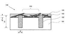
- FIG. 1 is a schematic configuration diagram of a transparent electrode 100 according to this embodiment.
- the transparent electrode 100 includes a transparent substrate 101, a metal grid 102; metal nanowires 103; and a neutral polythiophene mixture 104 .
- Various resin materials can be used as the material of the transparent substrate 101 .
- curable resin materials such as epoxy resins, acrylic resins and silicone resins
- thermoplastic resin materials such as polyethylene phthalate (PET) and polyethylene naphthalate (PEN). Materials formed by curing highly fluid monomers or oligomers are particularly preferred from the standpoint of production.
- the thickness of the transparent substrate is not particularly limited, it is, for example, 50 to 150 ⁇ m. Further, the total transmittance of the transparent substrate alone at 550 nm is preferably 85% or more.
- the transparent electrode according to the embodiment has a metal grid 102 .
- the metal grid preferably has a thickness d1 of 5-50 ⁇ m, more preferably 15-30 ⁇ m.
- the metal grid 102 forms an embedded portion embedded in the transparent substrate 101 and a projecting portion projecting from the surface of the transparent substrate.
- the height d2 of the protrusion exceeds 0 ⁇ m, but is preferably 1 ⁇ m or less, more preferably 0.1 to 0.7 ⁇ m, still more preferably 0.2 to 0.5 ⁇ m.
- the conductivity of the metal grid can be increased.
- the protruding metal grid facilitates electrical contact with the silver nanowires, and electrical contact with another layer to be bonded together when manufacturing the device.
- the height of the protrusions of the metal grid can be measured by scanning the surface using an atomic force microscope (AFM) or, for larger areas, a contact-type profilometer.
- the height of the protrusion is the average value of the measurement results at five randomly selected points.
- the thickness d1 of the metal grid 102 is 5 ⁇ m or more, the resistance of the metal grid wiring can be made extremely small. In addition, it is easy to handle the metal foil. If the thickness is less than 5 ⁇ m, a backing film is likely to be required for handling, resulting in high cost. On the other hand, when the thickness d1 is 50 ⁇ m or less, sufficient conductivity can be obtained, cost can be suppressed, and patterning can be easily performed. When the height d2 of the protruding portion of the metal grid is 1 ⁇ m or less, the small d2 makes it easy to prevent a short circuit when an element is produced using this transparent electrode.
- the line width d3 of the metal grid is adjusted according to the purpose, but it is preferably 10 to 100 ⁇ m, more preferably 20 to 50 ⁇ m.
- the line width of the metal grid is preferably 10 to 100 ⁇ m, more preferably 20 to 50 ⁇ m.
- the sheet resistance of the transparent electrode can be reduced.
- the light transmittance of the transparent electrode can be increased by setting the line width to 100 ⁇ m or less.
- d1, d2 and d3 are average values.
- the line width of the metal grid can be measured with a scanning electron microscope (SEM). In an embodiment, the line width of the metal grid is the average value of measurements at five randomly selected points.
- the metal grid is preferably made of copper, aluminum, silver, gold, tungsten, or alloys thereof, and more preferably made of copper or aluminum, which have relatively low electrical resistance.
- metal foils of these metals it is preferable to use metal foils of these metals as a raw material because it facilitates the production of metal grids.
- An exposed part 105 where the transparent base material is exposed is formed in the part where the metal grid is not arranged.
- the transparent electrode according to the embodiment comprises metal nanowires.
- the metal nanowires are placed in contact with the exposed surface of the transparent substrate or the protrusions of the metal grid.
- the metal contained in the metal nanowires is not particularly limited. Nanowires made of alloys are particularly preferred.
- a plurality of metal nanowires partially contact or fuse with each other to form a network-like structure such as a mesh or a lattice. In this way, a plurality of conductive paths are formed, forming a continuous conductive cluster (percolation conductive theory).
- a high density of nanowires is preferred to enhance the conductivity of such conductive clusters.
- the density of nanowires is below a certain level.
- the coating amount of nanowires in embodiments is generally 0.05 to 50 g/m 2 , preferably 0.1 to 10 g/m 2 , more preferably 0.15 to 1 g/m 2 . be. When the density of the metal nanowires is within this range, the resulting conductive film can achieve both sufficient transparency, flexibility and conductivity.
- the metal nanowires are usually composed of metal nanowires with a diameter of 10-500 nm and a length of 0.1-50 ⁇ m. In general, longer nanowires are more likely to form conductive clusters, and larger diameter nanowires are more conductive. Since a network structure is formed by using nanowires in this way, a conductive film containing nanowires exhibits high conductivity as a whole, although the amount of metal is small.
- the diameter of the nanowires is preferably 10-500 nm, more preferably 20-150 nm, particularly preferably 30-120 nm.
- the length of the nanowires is preferably 0.1-50 ⁇ m, more preferably 1-40 ⁇ m, particularly preferably 5-30 ⁇ m.
- the diameter and length of metal nanowires can be measured, for example, by analyzing SEM images obtained by a scanning electron microscope (SEM). In embodiments, nanowire diameters and lengths are averaged from measurements of five randomly selected nanowires.
- a transparent electrode according to an embodiment comprises a neutral polythiophene mixture.
- the neutral polythiophene mixture is placed in contact with the exposed surface of the transparent substrate or the protrusions of the metal grid.
- Polythiophene is a polymer of polythiophene or its derivatives and is used in various electronic devices due to its good conductivity. Of those polythiophenes, those that are neutral are used in embodiments. Polythiophene becomes conductive by doping.
- polythiophene and a doping agent such as polystyrene sulfonic acid are dispersed in water, and a small amount of dimethylsulfoxide is used as an additive to prepare a composition. Then, the composition is heated for film formation to prepare a transparent conductive film.
- compositions used in such cases are generally acidic, and such compositions tend to corrode metal grids and metal nanowires.
- Various types of neutral polythiophene mixtures are known, for example, polysulfonic acid polyamine salts are used as doping agents, and any one of them can be used depending on the purpose. In the embodiment, among them, those having a pH of 5 to 7 when prepared as an aqueous dispersion having a concentration of 1% by mass are preferable.
- a neutral polythiophene mixture for example, a mixture of poly(3,4-ethylenedioxythiophene) and guanidine salt of polystyrenesulfonic acid is preferably used.
- the applied amount of the neutral polythiophene mixture in embodiments is generally 0.01 to 0.5 g/m 2 , preferably 0.02 to 0.3 g/m 2 , more preferably 0.05 to 0.2 g / m2 .
- the coating amount of the neutral polythiophene mixture is within this range, the resulting conductive film can achieve both sufficient transparency, flexibility and conductivity.
- both the metal nanowires and the neutral polythiophene mixture are in contact with the protrusions of the metal grid.
- Oxide is usually formed on the surface of the metal grid, and the presence of the oxide increases the contact resistance with the metal nanowires. Therefore, it is preferable to remove the oxide to expose the metal surface and contact the metal nanowires before contacting the metal nanowires. That is, it is preferable to have a structure in which the metal surface of the metal grid and the metal nanowires are in contact with each other.
- Some of the molecules of the neutral polythiophene permeate between the particles of the metal nanowires to form a mixed layer in which the metal nanowires and the neutral polythiophene mixture are mixed with each other, and the conductivity of the mixed layer is increased. As a result, the conductivity of the transparent electrode also increases. And since the neutral polythiophene mixture coats the metal nanowires and metal grids, they are inhibited from being oxidized. Also, the neutral polythiophene mixture has the effect of suppressing metal migration. Therefore, metal ions derived from, for example, a photoelectric conversion layer included in the element are less likely to migrate to other layers, and the life of the element can be extended.
- the neutral polythiophene mixture tends to be easily adsorbed to the transparent substrate and the metal grid, and exerts an effect of compressing the metal nanowire layer.
- the contact area between metal nanowire particles increases, and the conductivity of the transparent electrode tends to increase.
- the transparent electrode according to the embodiment exhibits excellent conductivity by having the structure having the metal grid, metal nanowires, and neutral polythiophene mixture described above, and the sheet resistance of the transparent electrode is preferably 0.01 to 0.01. It is 1 ⁇ / ⁇ , more preferably 0.05 to 0.2 ⁇ / ⁇ . If the sheet resistance of the transparent electrode is less than 0.01 ⁇ , the light transmittance tends to be low. If the resistance is greater than 1 ⁇ , there is a tendency that strip-shaped scribing is required when constructing a large-area element.
- the [sheet resistance of the metal grid] is the sheet resistance of the composite of the transparent substrate and the metal grid placed thereon, and the [sheet resistance of the film made of metal nanowires] is the sheet resistance of the transparent substrate.
- the sheet resistance of the composite of the material and the metal nanowires arranged thereon [the sheet resistance of the film composed of the neutral polythiophene mixture], is the transparent substrate and the neutral polythiophene mixture arranged thereon. is the sheet resistance of the composite of
- the film made of metal nanowires has a sheet resistance of 20 to 50 ⁇ / ⁇
- the film made of a neutral polythiophene mixture has a sheet resistance of 100 to 500 ⁇ / ⁇ .
- Sheet resistance can be measured using the four-probe method. In the embodiment, the sheet resistance is the average value of five randomly selected sheet resistance values.
- the sheet resistance of the film made of metal nanowires is 20 ⁇ or more, sufficient light transmittance tends to be obtained, and when it is 50 ⁇ or less, the sheet resistance of the entire transparent electrode tends to decrease.
- the sheet resistance of the film made of the neutral polythiophene mixture is 100 ⁇ or more, sufficient light transmittance tends to be obtained, and when it is 500 ⁇ or less, the sheet resistance of the entire transparent electrode tends to decrease.
- the transparent electrode according to the present embodiment preferably has an aperture ratio of 90 to 99%, which is the surface area ratio of the exposed portion 105 of the transparent substrate to the surface area of the transparent electrode. If the aperture ratio is 90% or more, the light transmittance can be increased. On the other hand, by setting the aperture ratio to 99% or less, the line width of the metal grid can be increased and the sheet resistance can be decreased.
- the average surface roughness of the surface of the exposed portion 105 of the transparent substrate is 10 nm or less.
- the uniformity and stability of the device formed on the transparent electrode tend to be improved when forming a large-area device using the transparent electrode according to the embodiment. It is in. More preferably, the surface roughness of the exposed portion is 6 nm or less.
- Surface roughness can be measured by scanning the surface using an atomic force microscope (AFM). In an embodiment, the average value of the measured values of five randomly selected exposed portions of 5 ⁇ m square is used as the surface roughness.
- the transparent electrode according to the present embodiment it is preferable to further include a hydrophilic polymer film on the surface of the exposed portion 105 of the transparent substrate.
- the exposed surfaces can be coated with a film having relatively low surface roughness.
- a surface treatment agent such as alkylthiol
- the hydrophilic polymer is less likely to coat the metal grid portion.
- the length of the alkyl group of the alkylthiol is preferably from 2 to 12 carbon atoms. Alkylthiols can be removed from the metal grid surface by washing with acid.
- the transparent electrode according to the present embodiment preferably further comprises a graphene layer on the surface of the projections of the metal grid, the surface of the metal nanowires, or the surface of the neutral polythiophene mixture.
- the graphene layer has a structure in which one to several layers of sheet-shaped graphene are laminated.
- the number of laminated graphene layers is not particularly limited, but it is preferably 1 to 6 layers, and 2 to 4 layers so that sufficient transparency, conductivity, or ion shielding effect can be obtained. It is more preferable to have
- the graphene preferably has a structure in which a polyalkyleneimine, particularly a polyethyleneimine chain, such as shown in the following formula, is bonded to the graphene skeleton. It is also preferred that some of the carbons in the graphene skeleton are substituted with nitrogen.
- a polyethyleneimine chain is exemplified as a polyalkyleneimine chain.
- the number of carbon atoms contained in the alkyleneimine unit is preferably from 2 to 8, and polyethyleneimine containing a unit with 2 carbon atoms is particularly preferred.
- polyalkyleneimine having a branched chain or cyclic structure can also be used.
- n (the number of repeating units) is preferably 10-1000, more preferably 100-300.
- Graphene is preferably unsubstituted or nitrogen-doped. Nitrogen-doped graphene is preferred when a transparent electrode is used as the cathode.
- the doping amount (N/C atomic ratio) can be measured by X-ray photoelectron spectrum (XPS), and is preferably 0.1 to 30 atom %, more preferably 1 to 10 atom %.
- the graphene layer has a high shielding effect, prevents deterioration of metal oxides and metals by preventing diffusion of acids and halogen ions, and can prevent impurities from entering the photoelectric conversion layer from the outside. Furthermore, since the nitrogen-substituted graphene layer (N-graphene layer) contains nitrogen atoms, it has a high acid trapping ability, and thus has a higher shielding effect.
- inorganic oxide layer on top of the neutral polythiophene mixture or on top of the graphene layer.
- Inorganic oxides include TiO 2 , SnO 2 , WO 3 , NiO, MoO 3 , ZnO, V 2 O 5 and the like.
- a conductive oxide may be further laminated. These inorganic oxide layers function as barrier layers, insulating layers, buffer layers, etc. in transparent substrates or electronic devices. The ratio of metal to oxygen atoms in the inorganic oxide need not be stoichiometric.
- FIG. 2 The manufacturing method of the transparent electrode 100 according to the second embodiment shown in FIG. (A) a step of preparing a temporary support 201; (B) placing a metal grid 102 on the temporary support; (C) embedding a portion of the metal grid in the transparent substrate; (D) The transparent substrate 101 and the temporary support 201 are peeled off, and the metal grid 102 is removed so that the remaining part of the metal grid 102 forms a projecting portion projecting from the surface of the transparent substrate 101 . on the transparent substrate 101; (E) placing the metal nanowires 103 in contact with the protrusions of the metal grid 102; (F) placing a neutral polythiophene mixture 104 in contact with the protrusions of the metal grid 102;
- a temporary support 201 is prepared.
- This temporary support 201 is a support for temporarily placing the metal grid, and can be selected from any material.
- As a material for the temporary support 201 glass, resin film, metal, or the like is used.
- a metal grid 102 is arranged on the surface of the prepared temporary support 201 .
- This metal grid can be arranged by any method, for example, (i) a method of attaching a metal foil on the temporary support 201 and patterning the metal foil by a lithographic method, or (ii) a method of temporarily supporting It can be arranged on the body 201 by a printing method or a transfer method using ink containing metal. In any method, it is preferable to adjust the thickness of the metal foil and the amount of ink containing metal placed on the temporary support so that the thickness of the metal grid is 5 to 50 ⁇ m.
- step (C) part of the metal grid 102 formed on the surface of the temporary support 201 is embedded in the transparent substrate 101 .
- part of the metal grid 102 formed on the surface of the temporary support 201 is embedded in the transparent substrate 101 .
- the temporary support 201 on which the metal grid 102 is placed is inverted and pushed into the transparent substrate 101 .
- a groove may be mechanically formed in a transparent substrate having a high hardness, and a metal grid may be fitted in the groove.
- step (D) the temporary support is peeled off from the transparent base material 101 .
- a remaining part of the metal grid 102 becomes a projecting portion projecting from the surface of the transparent base material 101 .
- the transparent substrate is formed by curing a highly fluid monomer or oligomer, it often shrinks during curing.
- part of the metal grid protrudes from the surface of the transparent substrate as the transparent substrate precursor shrinks as it cures.
- the height of the projecting portion of the metal grid can be adjusted by controlling the temperature and time for curing the transparent base material.
- the temporary support may be removed after curing the transparent base material.
- oxide may be formed on the surface of the metal grid 102, especially on the protrusions. Such oxides cause performance deterioration of the transparent electrode and the device, and are therefore preferably removed.
- the surface of the transparent substrate is brought into contact with a reducing agent such as hydrazine hydrate for reduction treatment, or washed with an acid to remove oxides on the surface of the metal grid. can be done.
- the protruding portions of the metal grid can be subjected to a hydrophobizing treatment to form a hydrophilic polymer film on the surface of the exposed portion of the transparent base material.
- a hydrophobizing treatment to form a hydrophilic polymer film on the surface of the exposed portion of the transparent base material.
- step (E) metal nanowires 103 are arranged so as to be in contact with metal grid 102 .
- This step is generally carried out by applying a dispersion containing metal nanowires 103 to the surface of the transparent substrate.
- the dispersion can contain, for example, a polymer.
- the polymer functions as a binder for the metal nanowires, or improves the adhesiveness between the conductive film and the transparent substrate, thereby suppressing peeling of the conductive film.
- adhesive polymers for example, can be used for such applications.
- examples of such adhesive polymers include polyolefins, acrylic polymers, and polyurethane polymers into which polar groups have been introduced.
- the content of components other than metal nanowires is preferably low.
- the content of metal nanowires contained in the conductive film is preferably 95% by mass or more based on the total mass of the conductive film.
- step (F) the neutral polythiophene mixture 104 is placed in contact with the metal grid 102 .
- This step is generally performed by applying a solution or dispersion containing the neutral polythiophene mixture 104 to the surface of the transparent substrate on which the metal nanowires are arranged.
- the coating liquid containing the neutral polythiophene mixture contains water, ethanol, isopropyl alcohol, methyl ethyl ketone, etc. as a solvent or dispersion medium.
- step (E) or (F), or both can be performed by meniscus coating.
- the production efficiency can be improved by producing the transparent electrode by a roll-to-roll combination of coating methods. .
- a step of forming a graphene layer can be further combined after step (D), (E), or (F).
- the step of forming the graphene layer can be performed by any method.
- a method of forming a graphene film on another support and transferring it onto the structure can be adopted.
- an unsubstituted single-layer graphene film is formed by a CVD method using methane, hydrogen, and argon as reaction gases and using a copper foil as a base catalyst layer.
- single-layer graphene can be transferred onto the structure.
- a plurality of monolayer graphene layers can be laminated on the structure by repeating the same operation. At this time, it is preferable to form two to four graphene layers.
- Graphene in which some carbons are substituted with boron may be used instead of unsubstituted graphene.
- Boron-substituted graphene can be similarly prepared using BH 3 , methane, hydrogen, and argon as reactant gases.
- the fabrication method according to the embodiment can further have a step of forming an inorganic oxide layer after step (F) or after forming the graphene layer.
- Inorganic oxides include TiO 2 , SnO 2 , WO 3 , NiO, MoO 3 , ZnO, V 2 O 5 and the like. These inorganic oxide films are generally formed by a sputtering method, a vapor deposition method, a sol-gel method, or the like. The ratio of metal to oxygen atoms in the inorganic oxide need not be stoichiometric.
- FIG. 3 is a schematic configuration diagram of a solar cell 300 (photoelectric conversion element) according to this embodiment.
- the photovoltaic cell 300 is an element having a function as a photovoltaic cell that converts light energy such as sunlight L incident on the cell into electric power.
- a solar cell 300 includes a photoelectric conversion layer 302 provided on the surface of a transparent electrode 301 and a counter electrode 303 provided on the side of the photoelectric conversion layer 302 opposite to the transparent electrode 301 .
- the transparent electrode 301 is the same as that shown in the first embodiment.
- the photoelectric conversion layer 302 is a semiconductor layer that converts light energy of incident light into power to generate current.
- the photoelectric conversion layer 302 generally comprises a p-type semiconductor layer and an n-type semiconductor layer.
- a photoelectric conversion layer a laminate of a p-type polymer and an n-type material, RNH 3 PbX 3 (X is a halogen ion, R is an alkyl group, etc.), a silicon semiconductor, InGaAs, GaAs, chalcopyrite, CdTe, InP, etc. , SiGe-based, Cu 2 O-based inorganic compound semiconductors, quantum dot-containing type, and dye-sensitized transparent semiconductors may also be used. In either case, the efficiency is high, and deterioration of the output can be further reduced.
- a buffer layer may be inserted between the photoelectric conversion layer 302 and the transparent electrode 301 to promote or block charge injection.
- the counter electrode 303 is normally an opaque metal electrode, but a transparent electrode according to the embodiment may also be used. Another charge buffer layer or charge transport layer may be inserted between the counter electrode 303 and the photoelectric conversion layer 302 .
- anode buffer layers and charge transport layers examples include vanadium oxide, PEDOT/PSS, p-type polymer, vanadium pentoxide (V2O5), 2,2',7,7'-Tetrakis [N,N-di(4- methoxyphenyl)amino]-9,9′-spirobifluorene (hereinafter referred to as Spiro-OMeTAD), nickel oxide (NiO), tungsten trioxide (WO 3 ), molybdenum trioxide (MoO 3 ), etc. can be used. .
- the ratio of metal to oxygen atoms in the inorganic oxide need not be stoichiometric.
- the counter electrode 303 an electrode having the same structure as the transparent electrode 301 may be used. Further, the counter electrode 303 may contain unsubstituted planar single-layer graphene. Unsubstituted single-layer graphene can be produced by a CVD method using methane, hydrogen, and argon as reaction gases and using a copper foil as an underlying catalyst layer. For example, after the thermal transfer film and monolayer graphene are pressure-bonded, the copper is melted and the monolayer graphene is transferred onto the thermal transfer film. A plurality of monolayer graphene layers can be laminated on the thermal transfer film by repeating the same operation, producing 2 to 4 graphene layers.
- a counter electrode can be formed by printing a current-collecting metal wiring on this film using a silver paste or the like.
- Graphene in which some carbons are substituted with boron may be used instead of unsubstituted graphene.
- Boron-substituted graphene can be similarly prepared using BH 3 , methane, hydrogen, and argon as reactant gases. These graphenes can also be transferred from thermal transfer films onto suitable substrates such as PET.
- these single-layer or multilayer graphenes may be doped with tertiary amines as electron donor molecules.
- An electrode made of such a graphene film also functions as a transparent electrode.
- the solar cell according to the embodiment can have a structure sandwiched between transparent electrodes on both sides.
- a solar cell having such a structure can efficiently utilize light from both sides.
- the energy conversion efficiency is generally 5% or more, and it is characterized by long-term stability and flexibility.
- an ITO glass transparent electrode can be used as the counter electrode 303 instead of the graphene film. In this case, the flexibility of the solar cell is sacrificed, but light energy can be utilized with high efficiency. Also, stainless steel, copper, titanium, nickel, chromium, tungsten, gold, silver, molybdenum, tin, zinc, or the like may be used as the metal electrode. In this case, transparency tends to decrease.
- the solar cell can have an ultraviolet cut layer and a gas barrier layer.
- UV absorbers include 2-hydroxy-4-methoxybenzophenone, 2,2-dihydroxy-4-methoxybenzophenone, 2-hydroxy-4-methoxy-2-carboxybenzophenone, 2-hydroxy-4-n- Benzophenone compounds such as octoxybenzophenone; 2-(2-hydroxy-3,5-di-tert-butylphenyl)benzotriazole, 2-(2-hydroxy-5-methylphenyl)benzotriazole, 2-(2-hydroxy benzotriazole-based compounds such as 5-tertiary-octylphenyl)benzotriazole; and salicylic acid ester-based compounds such as phenyl salicylate and p-octylphenyl salicylate.
- the gas barrier layer a layer that blocks water vapor and oxygen is particularly preferable, and a layer that hardly allows water vapor to pass through is particularly preferable.
- layers made of inorganic substances such as SiN, SiO 2 , SiC, SiO x N y , TiO 2 and Al 2 O 3 , ultra-thin glass, and the like can be suitably used.
- the thickness of the gas barrier layer is not particularly limited, it is preferably in the range of 0.01 to 3000 ⁇ m, more preferably in the range of 0.1 to 100 ⁇ m. If the thickness is less than 0.01 ⁇ m, sufficient gas barrier properties tend not to be obtained.
- the water vapor transmission rate (water vapor permeability) of the gas barrier layer is preferably 100 g/m 2 ⁇ d to 10 -6 g/m 2 ⁇ d, more preferably 10 g/m 2 ⁇ d to 10 -5 g/m 2 ⁇ d, more preferably 1 g/m 2 ⁇ d to 10 -4 g/m 2 ⁇ d.
- the moisture permeability can be measured based on JIS Z0208 or the like.
- a dry method is suitable for forming the gas barrier layer.
- Methods for forming a gas barrier layer with gas barrier properties by a dry method include resistance heating deposition, electron beam deposition, induction heating deposition, vacuum deposition methods such as assisted methods using plasma or ion beams, reactive sputtering methods, and ion beams.
- Sputtering method sputtering method such as ECR (electron cyclotron) sputtering method, physical vapor deposition method (PVD method) such as ion plating method, chemical vapor deposition method (CVD method) using heat, light, plasma, etc.
- PVD method physical vapor deposition method
- CVD method chemical vapor deposition method
- the type of substrate is selected according to the purpose.
- an inorganic material such as glass, or an organic material such as PET, PEN, polycarbonate, or PMMA is used.
- a flexible organic material because the transparent electrode according to the embodiment becomes highly flexible.
- the solar cell of this embodiment can also be used as an optical sensor.
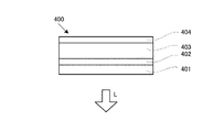
- FIG. 4 is a schematic configuration diagram of an organic EL element 400 (photoelectric conversion element) according to this embodiment.
- the organic EL element 400 is an element that functions as a light-emitting element that converts electrical energy input to this element into light L.
- the organic EL element 400 includes a photoelectric conversion layer (light-emitting layer) 402 provided on the surface of a transparent electrode 401 and a counter electrode 403 provided on the side of the photoelectric conversion layer 402 opposite to the transparent electrode 401 .
- the transparent electrode 401 here is the same as that shown in the first embodiment.
- the photoelectric conversion layer 402 is an organic thin film layer that recombines charges injected from the transparent electrode 401 and charges injected from the counter electrode 43 to convert electrical energy into light.
- the photoelectric conversion layer 402 usually consists of a p-type semiconductor layer and an n-type semiconductor layer.
- a buffer layer is provided between the photoelectric conversion layer 402 and the counter electrode 403 to promote or block charge injection, and another buffer layer may be provided between the photoelectric conversion layer 402 and the transparent electrode 401 .
- the counter electrode 403 is normally a metal electrode, but may be a transparent electrode.
- Example 1 A transparent electrode 500 having the structure shown in FIG. 5 is produced.
- a copper foil with a film thickness of 20 ⁇ m is pasted on a PET film with a thickness of 100 ⁇ m.
- 20 ⁇ m-wide rectangular lattice-like wiring is produced at a pitch of 2 mm by photolithography.
- the aperture ratio is 98%.
- an epoxy resin is applied and cured, and then peeled off from the PET film.
- the copper wiring 502 is embedded in the epoxy resin 501, the thickness of the metal grid is about 20 ⁇ m corresponding to the thickness of the copper foil, and the average difference between the protrusions is 0.5 ⁇ m. .
- An aqueous dispersion of silver nanowires with an average diameter of 30 nm and a length of 5 ⁇ m is meniscus-coated and then dried to form a silver nanowire layer 503 .
- the sheet resistance of the resulting film is 0.2 ⁇ on average.
- the average sheet resistance of the silver nanowire film coated on the PET film is 40 ⁇ .
- a neutral PEDOT aqueous dispersion of pH 6.0 (Clevios PJet) is meniscus-coated on the silver nanowire film to form a PEDOT layer 504 . After drying, the sheet resistance of the resulting film is 0.2 ⁇ .
- neutral PEDOT is similarly coated on the silver nanowire film of the PET film (average sheet resistance is 40 ⁇ ), the sheet resistance is 28 ⁇ on average, and the pressing effect of the PEDOT layer can be seen.
- the average roughness of the openings of the copper grid in AFM is 6 nm.
- Example 1 A transparent electrode is produced in the same manner as in Example 1, except that the step of removing copper oxide from the surface by washing with 1N hydrochloric acid and pure water and drying is not included.
- the sheet resistance of the obtained film measured with four probes was 40 ⁇ on average, and the metal nanowires and the metal grid were not in contact.
- Example 2 A transparent electrode is produced in the same manner as in Example 1, except that the thickness of the copper foil attached to the PET film is 4 ⁇ m. Since the copper foil is thin, it wrinkles and cannot be applied uniformly, making it difficult to form a grid having embedded and protruding portions.
- Example 2 Compared to the conditions in Example 1, the curing conditions for the epoxy resin are relaxed, and after curing, the epoxy resin is peeled off from the PET film. Observation by AFM shows that the copper wiring is embedded in the epoxy resin, and the height difference of the protruding portions is 0.1 ⁇ m on average.
- a transparent electrode is produced in the same manner as in Example 1 except for the above. The sheet resistance of the obtained transparent electrode film was 0.3 ⁇ on average, and the variation was larger than that of Example 1, and the contact between the metal nanowires and the metal grid was slightly inferior to that of Example 1.
- Example 3 In Example 1, the curing conditions of the epoxy resin are severer and cured more rapidly, and then the epoxy resin is peeled off from the PET film. Observation by AFM shows that the copper wiring is embedded in the epoxy resin, and the height difference of the protruding portions is 1.2 ⁇ m on average.
- a transparent electrode is produced in the same manner as in Example 1 except for the above. The average sheet resistance of the obtained transparent electrode film measured with four probes is 0.2 ⁇ .
- Example 4 On the transparent electrode of Example 1, a planar shielding layer is formed by laminating an average of four layers of N-graphene films in which some of the carbon atoms are substituted with nitrogen atoms.
- the shielding layer is created as follows. First, the surface of the Cu foil is heat-treated by laser irradiation and annealed to enlarge the crystal grains. Using this Cu foil as a base catalyst layer, using a mixed reaction gas of ammonia, methane, hydrogen, and argon (15:60:65:200 ccm) at 1000° C. for 5 minutes, a planar single-layer N-graphene was formed by a CVD method. Manufacture the membrane. At this time, a single-layer graphene film is mostly formed, but depending on the conditions, an N-graphene film having two or more layers is also partially formed. Further, it is treated at 1000° C.
- the single layer N-graphene film is transferred onto the thermal transfer film by immersing it in an ammonia alkaline cupric chloride etchant to dissolve Cu.
- an ammonia alkaline cupric chloride etchant to dissolve Cu.
- four monolayer graphene films are laminated on the thermal transfer film to obtain a multilayer N-graphene film. After laminating the thermal transfer film on the transparent electrode obtained in Example 1, it is heated to transfer the N-graphene film.
- the nitrogen content measured by XPS is 1-2 atom% under these conditions.
- the ratio of carbon atoms to oxygen atoms in the carbon material measured by XPS is 100-200.
- Example 5 A solar cell 600 shown in FIG. 6 is produced.
- a chlorobenzene solution containing poly(3-hexylthiophene-2,5-diyl) and C 60 -PCBM was meniscus-coated on the transparent electrode 601 obtained in Example 1, and dried at 100° C. for 20 minutes.
- a conversion layer 602 is fabricated.
- a toluene solution of C 60 -PCBM is meniscus-coated and dried to form an electron transport layer 603 .
- an aqueous solution of lithium fluoride is applied as the electron injection layer 604 .
- a counter electrode 605 is produced by vapor-depositing aluminum thereon.
- An ultraviolet cut layer 66 is produced by screen-printing an ultraviolet cut ink containing 2-hydroxy-4-methoxybenzophenone on the surface of the transparent substrate.
- a silica film is formed on the ultraviolet shielding layer by a vacuum evaporation method to form a gas barrier layer 67, and the whole is sealed with a film to produce a solar battery cell 60.
- the resulting solar cell exhibits an energy conversion efficiency of 5% or more for 1 SUN of sunlight.
- Example 6 A solar cell is produced in the same manner as in Example 5, except that the transparent electrode obtained in Example 3 is used.
- the obtained solar cells include those exhibiting an energy conversion efficiency of 5% or more with respect to 1 SUN of sunlight, and those that are short-circuited.
- Example 7 Create an organic EL element.
- An aqueous solution of lithium fluoride was applied as an electron transport layer on the transparent electrode obtained in Example 4, and tris(8-hydroxyquinoline) aluminum (Alq 3 ) (40 nm), which also functions as an n-type semiconductor and is also a light-emitting layer, was applied. ) to produce a photoelectric conversion layer.
- NPD N,N'-di-1-naphthyl-N,N'-diphenyl-1,1'-biphenyl-4,4'-diamine
- Layer 83 is made.
- a gold electrode is formed thereon by a sputtering method. Further, by sealing the periphery, an organic EL element is produced.
- the obtained organic EL device has an efficiency of 20% or more.
- a titanium oxide film is formed on the transparent electrode obtained in Example 4 by sputtering. Meniscus a solution of PbI 2 in isopropanol. A solution of methylammonium iodide in isopropanol is then meniscus coated. A photoelectric conversion layer is produced by drying at 100 degreeC for 10 minutes. Next, a toluene solution of Spiro-OMeTAD is meniscus-coated and dried to form a hole transport layer. An aqueous solution obtained by adding sorbitol to PEDOT/PSS is applied thereon and dried at 100° C. for 10 minutes to form a conductive adhesive layer.
- Example 4 The other transparent electrode obtained in Example 4 and the adhesive layer are bonded together.
- An ultraviolet shielding ink containing 2-hydroxy-4-methoxybenzophenone is screen-printed on the surface of the laminated transparent substrate to form an ultraviolet shielding layer.
- a silica film is formed on the ultraviolet shielding layer by a vacuum deposition method to form a gas barrier layer, thereby producing a translucent solar cell.
- the resulting solar cell exhibits an energy conversion efficiency of 10% or more for 1 SUN of sunlight.
- Example 8 A four-terminal tandem photovoltaic cell 700 shown in FIG. 7 is produced.
- a solar cell 703 provided with a transparent electrode 703a according to the embodiment obtained in Example 7 is arranged on a monocrystalline silicon solar cell 701 with an intermediate layer 702 for adhesion interposed therebetween. It is
- the resulting solar cell exhibits an energy conversion efficiency of 22% or more for 1 SUN of sunlight.
Abstract
Description
透明基材と、
金属グリッドと、
金属ナノワイヤと、
中性ポリチオフェン混合物と
を含む構造を具備し、
前記金属グリッドは前記透明基材に埋設された埋設部と、前記透明基材から突出した突出部を有し、
前記金属ナノワイヤおよび前記中性ポリチオフェン混合物が、前記透明基材または前記金属グリッドの前記突出部に接触するように配置されていることを特徴とするものである。 A transparent electrode according to an embodiment comprises:
a transparent substrate;
a metal grid;
metal nanowires;
a structure comprising a mixture of neutral polythiophenes,
The metal grid has an embedded portion embedded in the transparent substrate and a protruding portion protruding from the transparent substrate,
The metal nanowires and the neutral polythiophene mixture are arranged so as to contact the protrusions of the transparent substrate or the metal grid.
(A)仮支持体を準備する工程、
(B)前記仮支持体の上に、金属グリッドを配置する工程、
(C)前記金属グリッドの一部を前記透明基材に埋設する工程、
(D)前記透明基材と前記仮支持体とを剥離し、前記金属グリッドの残余の一部が前記透明基材の表面から突出した突出部を形成するように前記金属グリッドを前記透明基材に配置する工程、
(E)金属ナノワイヤを前記金属グリッドの突出部に接触するように配置する工程、および
(F)中性ポリチオフェン混合物を前記金属グリッドの突出部に接触するように配置する工程
を含むことを特徴とするものである。 Further, the method for producing a transparent electrode according to the embodiment includes:
(A) a step of preparing a temporary support;
(B) placing a metal grid on the temporary support;
(C) embedding a portion of the metal grid in the transparent substrate;
(D) separating the transparent base material and the temporary support, and separating the metal grid from the transparent base material so that the remaining part of the metal grid forms a protruding part protruding from the surface of the transparent base material; placing in
(E) placing metal nanowires in contact with protrusions of the metal grid; and (F) placing a neutral polythiophene mixture in contact with protrusions of the metal grid. It is something to do.
まず、図1を用いて、第1の実施形態に係る透明電極の構成について説明する。図1は、本実施形態に係る透明電極100の構成概略図である。 [Embodiment 1]
First, the configuration of the transparent electrode according to the first embodiment will be described with reference to FIG. FIG. 1 is a schematic configuration diagram of a
透明基材101と、
金属グリッド102と、
金属ナノワイヤ103と、
中性ポリチオフェン混合物104と
を含む構造を具備している。 The
a
and a
[金属グリッドのシート抵抗]<[金属ナノワイヤからなる膜のシート抵抗]<[中性ポリチオフェン混合物からなる膜のシート抵抗]
の関係を満たすことが好ましい。このような関係を満たすことにより、透明電極の全体にわたって高い導電性と高い光透過性とを実現できる。ここで、[金属グリッドのシート抵抗]とは、透明基材とその上に配置された金属グリッドとの複合体のシート抵抗であり、[金属ナノワイヤからなる膜のシート抵抗]とは、透明基材と、その上に配置された金属ナノワイヤとの複合体のシート抵抗、[中性ポリチオフェン混合物からなる膜のシート抵抗]とは、透明基材と、その上に配置された中性ポリチオフェン混合物との複合体のシート抵抗である。 To achieve such high conductivity,
[Sheet resistance of metal grid] < [Sheet resistance of film composed of metal nanowires] < [Sheet resistance of film composed of neutral polythiophene mixture]
It is preferable to satisfy the relationship of By satisfying such a relationship, high conductivity and high light transmittance can be achieved over the entire transparent electrode. Here, the [sheet resistance of the metal grid] is the sheet resistance of the composite of the transparent substrate and the metal grid placed thereon, and the [sheet resistance of the film made of metal nanowires] is the sheet resistance of the transparent substrate. The sheet resistance of the composite of the material and the metal nanowires arranged thereon, [the sheet resistance of the film composed of the neutral polythiophene mixture], is the transparent substrate and the neutral polythiophene mixture arranged thereon. is the sheet resistance of the composite of

図2で示す第2の実施形態に係る透明電極100の作製方法は、
(A)仮支持体201を準備する工程、
(B)前記仮支持体の上に、金属グリッド102を配置する工程
(C)前記金属グリッドの一部を前記透明基材に埋設する工程、
(D)前記透明基材101と前記仮支持体201とを剥離し、前記金属グリッド102の残余の一部が前記透明基材101の表面から突出した突出部を形成するように前記金属グリッド102を前記透明基材101に配置する工程
(E)金属ナノワイヤ103を前記金属グリッド102の突出部に接触するように配置する工程、
(F)中性ポリチオフェン混合物104を前記金属グリッド102の突出部に接触するように配置する工程
を含む。 [Embodiment 2]
The manufacturing method of the
(A) a step of preparing a
(B) placing a
(D) The
(F) placing a
(i)仮支持体201の上に、金属箔を貼り付け、さらにリソグラフィ法によって金属箔をパターニングする方法、または
(ii)仮支持体201の上に金属を含むインキを用いた印刷法または転写法による方法
によって配置することができる。いずれの方法においても、金属グリッドの厚さが5~50μmとなるように、金属箔の厚さや仮支持体上に配置される金属を含むインキの量などを調整することが好ましい。 In step (B), a
図3を用いて、第3の電子デバイスの実施形態の一つに係る光電変換素子の構成について説明する。図3は、本実施形態に係る太陽電池セル300(光電変換素子)の構成概略図である。太陽電池セル300は、このセルに入射してきた太陽光L等の光エネルギーを電力に変換する太陽電池としての機能を有する素子である。太陽電池セル300は、透明電極301の表面に設けられた光電変換層302と、光電変換層302の透明電極301の反対側面に設けられた対向電極303とを具備している。ここで透明電極301は実施形態1で示されたものと同様である。 [Embodiment 3-1]
The configuration of a photoelectric conversion element according to one embodiment of the third electronic device will be described with reference to FIG. FIG. 3 is a schematic configuration diagram of a solar cell 300 (photoelectric conversion element) according to this embodiment. The
図4を用いて、第3の別の実施形態に係る光電変換素子の構成について説明する。図4は、本実施形態に係る有機EL素子400(光電変換素子)の構成概略図である。有機EL素子400は、この素子に入力された電気エネルギーを光Lに変換する発光素子としての機能を有する素子である。有機EL素子400は、透明電極401の表面に設けられた光電変換層(発光層)402と、光電変換層402の透明電極401の反対側面に設けられた対向電極403とを具備している。 [Embodiment 3-2]
A configuration of a photoelectric conversion element according to a third embodiment will be described with reference to FIG. FIG. 4 is a schematic configuration diagram of an organic EL element 400 (photoelectric conversion element) according to this embodiment. The
図5に示す構造の透明電極500を作成する。厚さ100μmのPETフィルム上に膜厚20μmの銅箔を張り付ける。レジストフィルムを張り付けた後、幅20μmの四角格子状の配線を2mmピッチで光リソグラフィ法で作製する。開口率は98%である。次にエポキシ樹脂を塗布、硬化させた後、PETフィルムから剥離する。 (Example 1)
A
1N塩酸、純水で洗浄、乾燥させて表面の銅酸化物を除去する工程を有しないことを除いては実施例1と同様にして透明電極を作製する。得られたフィルムの4探針で測定したシート抵抗は平均で40Ωであり、金属ナノワイアと金属グリッドとが接触していない。 (Comparative example 1)
A transparent electrode is produced in the same manner as in Example 1, except that the step of removing copper oxide from the surface by washing with 1N hydrochloric acid and pure water and drying is not included. The sheet resistance of the obtained film measured with four probes was 40Ω on average, and the metal nanowires and the metal grid were not in contact.
PETフィルムに貼り付ける銅箔の膜厚を4μmにした他は、実施例1と同様にして透明電極を作製する。銅箔が薄いためににしわが発生し、均一にはりつけることができず、埋設部と突出部を有するグリッドの形成が困難である。 (Comparative example 2)
A transparent electrode is produced in the same manner as in Example 1, except that the thickness of the copper foil attached to the PET film is 4 μm. Since the copper foil is thin, it wrinkles and cannot be applied uniformly, making it difficult to form a grid having embedded and protruding portions.
実施例1にの条件に対して、エポキシ樹脂の硬化条件をより緩和して、硬化させた後、PETフィルムから剥離する。AFMで観測するとエポキシ樹脂に銅配線は埋め込まれており、突出部の高さの差は平均で0.1μmである。他は実施例1と同様にして透明電極を作製する。
得られた透明電極フィルムのシート抵抗は平均で0.3Ωであり、バラツキが実施例1と比べて大きく、金属ナノワイアと金属グリッドとの接触が実施例1よりもわずかに劣る。 (Example 2)
Compared to the conditions in Example 1, the curing conditions for the epoxy resin are relaxed, and after curing, the epoxy resin is peeled off from the PET film. Observation by AFM shows that the copper wiring is embedded in the epoxy resin, and the height difference of the protruding portions is 0.1 μm on average. A transparent electrode is produced in the same manner as in Example 1 except for the above.
The sheet resistance of the obtained transparent electrode film was 0.3Ω on average, and the variation was larger than that of Example 1, and the contact between the metal nanowires and the metal grid was slightly inferior to that of Example 1.
実施例1においてエポキシ樹脂の硬化条件を厳しくしてより迅速に硬化させた後、PETフィルムから剥離する。AFMで観測するとエポキシ樹脂に銅配線は埋め込まれており、突出部の高さの差は平均で1.2μmである。他は実施例1と同様にして透明電極を作製する。得られた透明電極フィルムの4探針で測定したシート抵抗は平均で0.2Ωである。 (Example 3)
In Example 1, the curing conditions of the epoxy resin are severer and cured more rapidly, and then the epoxy resin is peeled off from the PET film. Observation by AFM shows that the copper wiring is embedded in the epoxy resin, and the height difference of the protruding portions is 1.2 μm on average. A transparent electrode is produced in the same manner as in Example 1 except for the above. The average sheet resistance of the obtained transparent electrode film measured with four probes is 0.2Ω.
実施例1の透明電極上に平面状の、炭素原子の一部が窒素原子に置換された、平均4層のN-グラフェン膜が積層された遮蔽層を形成する。 (Example 4)
On the transparent electrode of Example 1, a planar shielding layer is formed by laminating an average of four layers of N-graphene films in which some of the carbon atoms are substituted with nitrogen atoms.
図6に示す太陽電池セル600を作成する。
実施例1で得られる透明電極601上にポリ(3-ヘキシルチオフェン-2,5-ジイル)とC60-PCBMとを含むクロルベンゼン溶液をメニスカス塗布し、100℃で20分乾燥することにより光電変換層602を作製する。次にC60-PCBMのトルエン溶液をメニスカス塗布して乾燥させ、電子輸送層603を作製する。次に電子注入層604としてフッ化リチウムの水溶液を塗布する。その上にアルミニウムを蒸着し、対向電極605を作製する。 (Example 5)
A
A chlorobenzene solution containing poly(3-hexylthiophene-2,5-diyl) and C 60 -PCBM was meniscus-coated on the
実施例3で得られる透明電極を用いることを除いては実施例5と同様にして太陽電池セルを作製する。
得られる太陽電池セルは1SUNの太陽光に対して5%以上のエネルギー変換効率を示すものと、短絡しているものが混在する。 (Example 6)
A solar cell is produced in the same manner as in Example 5, except that the transparent electrode obtained in Example 3 is used.
The obtained solar cells include those exhibiting an energy conversion efficiency of 5% or more with respect to 1 SUN of sunlight, and those that are short-circuited.
有機EL素子を作成する。実施例4で得られる透明電極上に電子輸送層としてフッ化リチウムの水溶液を塗布し、n型の半導体としても機能し、発光層でもあるトリス(8-ヒドロキシキノリン)アルミニウム(Alq3)(40nm)を蒸着して光電変換層を作製する。その上にN,N’-ジ-1-ナフチル-N,N’-ジフェニル-1,1’-ビフェニル-4,4’-ジアミン(以下、NPDという)を30nmの厚さで蒸着しホール輸送層83を作製する。その上に金電極をスパッタ法により製膜する。さらに周りを封止することにより有機EL素子を作製する。得られる有機EL素子は効率20%以上である。 (Example 7)
Create an organic EL element. An aqueous solution of lithium fluoride was applied as an electron transport layer on the transparent electrode obtained in Example 4, and tris(8-hydroxyquinoline) aluminum (Alq 3 ) (40 nm), which also functions as an n-type semiconductor and is also a light-emitting layer, was applied. ) to produce a photoelectric conversion layer. N,N'-di-1-naphthyl-N,N'-diphenyl-1,1'-biphenyl-4,4'-diamine (hereinafter referred to as NPD) was deposited thereon to a thickness of 30 nm to transport holes. Layer 83 is made. A gold electrode is formed thereon by a sputtering method. Further, by sealing the periphery, an organic EL element is produced. The obtained organic EL device has an efficiency of 20% or more.
太陽電池セルを作成する。 (Example 8)
Create a solar cell.
上記貼り合わせた透明基板表面に2-ヒドロキシ-4-メトキシベンゾフェノン含有の紫外線カットインクをスクリーン印刷して紫外線カット層を作製する。紫外線カット層の上に真空蒸着法でシリカ膜を製膜しガスバリア層を作製し半透明な太陽電池セルを作製する。 The other transparent electrode obtained in Example 4 and the adhesive layer are bonded together.
An ultraviolet shielding ink containing 2-hydroxy-4-methoxybenzophenone is screen-printed on the surface of the laminated transparent substrate to form an ultraviolet shielding layer. A silica film is formed on the ultraviolet shielding layer by a vacuum deposition method to form a gas barrier layer, thereby producing a translucent solar cell.
図7に示す4端子型タンデム太陽電池セル700を作成する。このタンデム太陽電池セルは、単結晶シリコン太陽電池セル701の上に、接着のための中間層702を挟んで、実施例7で得られる実施形態による透明電極703aを具備した太陽電池セル703が配置されている。 (Example 8)
A four-terminal tandem
101…透明基材
102…金属グリッド
103…金属ナノワイヤ
104…中性ポリチオフェン混合物
105…露出部
201…仮支持体
d1…金属グリッドの厚さ
d2…金属グリッドと開口部の高さの差
d3…金属グリッドの線幅
300…太陽電池セル
301…透明電極
302…光電変換層
303…対向電極
400…有機EL素子
401…透明電極
402…光電変換層
403…対向電極
500…透明電極
501…エポキシ樹脂
502…銅配線
503…銀ナノワイヤ層
504…PEDOT層
600…太陽電池セル
601…透明電極
602…光電変換層
603…電子輸送層
604…電子注入層
605…対向電極
606…紫外線カット層
607…ガスバリア層
700…タンデム太陽電池セル
701…単結晶シリコン太陽電池セル
702…中間層
703…太陽電池セル
703a…透明電極 DESCRIPTION OF
Claims (20)
- 透明基材と、
金属グリッドと、
金属ナノワイヤと、
中性ポリチオフェン混合物と
を含む構造を具備し、
前記金属グリッドは前記透明基材に埋設された埋設部と、前記透明基材から突出した突出部を有し、
前記金属ナノワイヤおよび前記中性ポリチオフェン混合物が、前記透明基材または前記金属グリッドの前記突出部に接触するように配置されている、透明電極。 a transparent substrate;
a metal grid;
metal nanowires;
a structure comprising a mixture of neutral polythiophenes,
The metal grid has an embedded portion embedded in the transparent substrate and a protruding portion protruding from the transparent substrate,
A transparent electrode, wherein the metal nanowires and the neutral polythiophene mixture are arranged to contact the protrusions of the transparent substrate or the metal grid. - 前記金属グリッドの厚さが5~50μmである、請求項1に記載の透明電極。 The transparent electrode according to claim 1, wherein the metal grid has a thickness of 5 to 50 µm.
- 前記突出部の高さが1μm以下である、請求項1または2に記載の透明電極。 The transparent electrode according to claim 1 or 2, wherein the protrusion has a height of 1 µm or less.
- 前記金属グリッドの線幅が10~100μmである、請求項1~3のいずれか1項に記載の透明電極。 The transparent electrode according to any one of claims 1 to 3, wherein the metal grid has a line width of 10 to 100 µm.
- 前記中性ポリチオフェン混合物が、中性ポリチオフェンとドーピング剤の混合物であり、前記中性ポリチオフェン混合物の濃度が1質量%の水中分散液としたときのpHが5~7であるものである、請求項1~4のいずれか1項に記載の透明電極。 The neutral polythiophene mixture is a mixture of a neutral polythiophene and a doping agent, and the neutral polythiophene mixture has a pH of 5 to 7 when dispersed in water with a concentration of 1% by mass. 5. The transparent electrode according to any one of 1 to 4.
- 前記中性ポリチオフェンが、ポリ(3,4-エチレンジオキシチオフェン)である、請求項1~5のいずれか1項に記載の透明電極。 The transparent electrode according to any one of claims 1 to 5, wherein the neutral polythiophene is poly(3,4-ethylenedioxythiophene).
- 前記透明電極のシート抵抗が0.01~1Ω/□である、請求項1~6のいずれか1項に記載の透明電極。 The transparent electrode according to any one of claims 1 to 6, wherein the transparent electrode has a sheet resistance of 0.01 to 1Ω/□.
- [前記金属グリッドのシート抵抗]<[前記金属ナノワイヤからなる膜のシート抵抗]<[前記中性ポリチオフェン混合物からなる膜のシート抵抗]
の関係を満たす、請求項1~7のいずれか1項に記載の透明電極。 [Sheet resistance of the metal grid]<[Sheet resistance of the film composed of the metal nanowires]<[Sheet resistance of the film composed of the neutral polythiophene mixture]
The transparent electrode according to any one of claims 1 to 7, which satisfies the relationship of - 前記透明電極の表面積を基準とした、前記透明基材の露出部表面の面積比である開口率が90~99%である、請求項1~8のいずれか1項に記載の透明電極。 The transparent electrode according to any one of claims 1 to 8, wherein the aperture ratio, which is the area ratio of the surface of the exposed portion of the transparent base material, is 90 to 99% based on the surface area of the transparent electrode.
- 前記透明基材の露出部表面の平均表面粗さが10nm以下である、請求項1~9のいずれか1項に記載の透明電極。 The transparent electrode according to any one of claims 1 to 9, wherein the average surface roughness of the surface of the exposed portion of the transparent substrate is 10 nm or less.
- 前記金属グリッドの突出部の表面、前記金属ナノワイヤの表面、または前記積層構造の表面に、グラフェン層をさらに具備する、請求項1~10のいずれか1項に記載の透明電極。 The transparent electrode according to any one of claims 1 to 10, further comprising a graphene layer on the surface of the protrusion of the metal grid, the surface of the metal nanowires, or the surface of the laminated structure.
- (A)仮支持体を準備する工程、
(B)前記仮支持体の上に、金属グリッドを配置する工程、
(C)前記金属グリッドの一部を前記透明基材に埋設する工程、
(D)前記透明基材と前記仮支持体とを剥離し、前記金属グリッドの残余の一部が前記透明基材の表面から突出した突出部を形成するように前記金属グリッドを前記透明基材に配置する工程、
(E)金属ナノワイヤを前記金属グリッドの突出部に接触するように配置する工程、および
(F)中性ポリチオフェン混合物を前記金属グリッドの突出部に接触するように配置する工程
を含む、透明電極の作製方法。 (A) a step of preparing a temporary support;
(B) placing a metal grid on the temporary support;
(C) embedding a portion of the metal grid in the transparent substrate;
(D) separating the transparent base material and the temporary support, and separating the metal grid from the transparent base material so that the remaining part of the metal grid forms a protruding part protruding from the surface of the transparent base material; placing in
(E) placing metal nanowires in contact with the protrusions of the metal grid; and (F) placing a neutral polythiophene mixture in contact with the protrusions of the metal grid. How to make. - 前記工程(B)が、前記仮支持体の上に金属箔を貼り付け、リソグラフィ法によって前記金属箔をパターニングすることにより行われる、請求項12に記載の作製方法。 The manufacturing method according to claim 12, wherein the step (B) is performed by attaching a metal foil onto the temporary support and patterning the metal foil by a lithographic method.
- 工程(B)の後に、前記金属グリッドの突出部の表面の酸化物を除去する工程をさらに含む、請求項12~13のいずれか1項に記載の作製方法。 The fabrication method according to any one of claims 12 to 13, further comprising a step of removing oxides on the surface of the protrusions of the metal grid after step (B).
- 工程(D)の後に、前記金属グリッド突出部を疎水化処理し、前記透明基材の露出部表面に親水性ポリマー膜を作製する工程をさらに含む、請求項12~14のいずれか1項に記載の作製方法。 15. The method according to any one of claims 12 to 14, further comprising, after step (D), the step of hydrophobizing the metal grid protrusions to form a hydrophilic polymer film on the surface of the exposed portion of the transparent substrate. Method of preparation as described.
- グラフェン層を形成する工程をさらに含む、請求項12~15のいずれか1項に記載の作製方法。 The fabrication method according to any one of claims 12 to 15, further comprising the step of forming a graphene layer.
- 請求項1~11のいずれか1項に記載の透明電極を具備する電子デバイス。 An electronic device comprising the transparent electrode according to any one of claims 1 to 11.
- 前記透明電極と、光電変換層と、対向電極とを具備する、請求項17に記載の電子デバイス。 The electronic device according to claim 17, comprising the transparent electrode, a photoelectric conversion layer, and a counter electrode.
- 前記光電変換層がハロゲンイオンを含む、請求項17または18に記載の電子デバイス。 The electronic device according to claim 17 or 18, wherein the photoelectric conversion layer contains halogen ions.
- 前記透明電極を4端子型タンデム太陽電池の透明電極として具備する、請求項17~19のいずれか1項に記載の電子デバイス。 The electronic device according to any one of claims 17 to 19, comprising the transparent electrode as a transparent electrode of a four-terminal tandem solar cell.
Priority Applications (5)
| Application Number | Priority Date | Filing Date | Title |
|---|---|---|---|
| EP21927033.7A EP4307395A1 (en) | 2021-03-12 | 2021-03-12 | Transparent electrode, method for producing same and electronic device using transparent electrode |
| PCT/JP2021/009945 WO2022190336A1 (en) | 2021-03-12 | 2021-03-12 | Transparent electrode, method for producing same and electronic device using transparent electrode |
| JP2022552396A JP7482240B2 (en) | 2021-03-12 | Transparent electrode, method for producing the same, and electronic device using the transparent electrode | |
| CN202180018129.3A CN115349179A (en) | 2021-03-12 | 2021-03-12 | Transparent electrode, method for manufacturing same, and electronic device using transparent electrode |
| US17/929,390 US20220416100A1 (en) | 2021-03-12 | 2022-09-02 | Transparent electrode, method for producing the same, and electronic device using transparent electrode |
Applications Claiming Priority (1)
| Application Number | Priority Date | Filing Date | Title |
|---|---|---|---|
| PCT/JP2021/009945 WO2022190336A1 (en) | 2021-03-12 | 2021-03-12 | Transparent electrode, method for producing same and electronic device using transparent electrode |
Related Child Applications (1)
| Application Number | Title | Priority Date | Filing Date |
|---|---|---|---|
| US17/929,390 Continuation US20220416100A1 (en) | 2021-03-12 | 2022-09-02 | Transparent electrode, method for producing the same, and electronic device using transparent electrode |
Publications (1)
| Publication Number | Publication Date |
|---|---|
| WO2022190336A1 true WO2022190336A1 (en) | 2022-09-15 |
Family
ID=83226457
Family Applications (1)
| Application Number | Title | Priority Date | Filing Date |
|---|---|---|---|
| PCT/JP2021/009945 WO2022190336A1 (en) | 2021-03-12 | 2021-03-12 | Transparent electrode, method for producing same and electronic device using transparent electrode |
Country Status (4)
| Country | Link |
|---|---|
| US (1) | US20220416100A1 (en) |
| EP (1) | EP4307395A1 (en) |
| CN (1) | CN115349179A (en) |
| WO (1) | WO2022190336A1 (en) |
Families Citing this family (1)
| Publication number | Priority date | Publication date | Assignee | Title |
|---|---|---|---|---|
| WO2022029862A1 (en) * | 2020-08-04 | 2022-02-10 | 株式会社 東芝 | Electrode evaluation method |
Citations (10)
| Publication number | Priority date | Publication date | Assignee | Title |
|---|---|---|---|---|
| WO2010001591A1 (en) * | 2008-07-04 | 2010-01-07 | 戸田工業株式会社 | Transparent electrically conductive transfer plate and production method therefor, transparent electrically conductive base, method for producing transparent electrically conductive base using transparent electrically conductive transfer plate, and molded article using transparent electrically conductive base |
| WO2011055663A1 (en) * | 2009-11-04 | 2011-05-12 | コニカミノルタホールディングス株式会社 | Transparent electrode and organic electronic device |
| JP2011116925A (en) * | 2009-12-04 | 2011-06-16 | Nihon Sentan Kagaku Kk | Method for producing dispersion of electroconductive composition comprising composite of conjugated double bond polymer with polystyrenesulfonate or polyvinylsulfonate |
| JP2011157535A (en) * | 2010-01-29 | 2011-08-18 | Nihon Sentan Kagaku Kk | Method of production of electroconductive composition |
| JP2012080091A (en) * | 2010-09-07 | 2012-04-19 | Fujifilm Corp | Transparent conductive film, method for manufacturing the film, and organic thin film solar cell using the film |
| WO2012093530A1 (en) * | 2011-01-06 | 2012-07-12 | リンテック株式会社 | Transparent conductive laminate body and organic thin film device |
| JP2013542546A (en) * | 2010-03-08 | 2013-11-21 | ウィリアム・マーシュ・ライス・ユニバーシティ | Transparent electrode based on graphene / lattice hybrid structure |
| JP2017080951A (en) * | 2015-10-26 | 2017-05-18 | 日東電工株式会社 | Hard coat film and transparent conductive film |
| JP6142870B2 (en) | 2012-04-05 | 2017-06-07 | コニカミノルタ株式会社 | Organic photoelectric conversion device and solar cell using the same |
| US20180248052A1 (en) * | 2015-01-08 | 2018-08-30 | Korea Research Institute Of Chemical Technology | Method for manufacturing device comprising inorganic/organic hybrid perovskite compound film and device comprising inorganic/organic hybrid perovskite compound film |
-
2021
- 2021-03-12 CN CN202180018129.3A patent/CN115349179A/en active Pending
- 2021-03-12 EP EP21927033.7A patent/EP4307395A1/en active Pending
- 2021-03-12 WO PCT/JP2021/009945 patent/WO2022190336A1/en active Application Filing
-
2022
- 2022-09-02 US US17/929,390 patent/US20220416100A1/en active Pending
Patent Citations (10)
| Publication number | Priority date | Publication date | Assignee | Title |
|---|---|---|---|---|
| WO2010001591A1 (en) * | 2008-07-04 | 2010-01-07 | 戸田工業株式会社 | Transparent electrically conductive transfer plate and production method therefor, transparent electrically conductive base, method for producing transparent electrically conductive base using transparent electrically conductive transfer plate, and molded article using transparent electrically conductive base |
| WO2011055663A1 (en) * | 2009-11-04 | 2011-05-12 | コニカミノルタホールディングス株式会社 | Transparent electrode and organic electronic device |
| JP2011116925A (en) * | 2009-12-04 | 2011-06-16 | Nihon Sentan Kagaku Kk | Method for producing dispersion of electroconductive composition comprising composite of conjugated double bond polymer with polystyrenesulfonate or polyvinylsulfonate |
| JP2011157535A (en) * | 2010-01-29 | 2011-08-18 | Nihon Sentan Kagaku Kk | Method of production of electroconductive composition |
| JP2013542546A (en) * | 2010-03-08 | 2013-11-21 | ウィリアム・マーシュ・ライス・ユニバーシティ | Transparent electrode based on graphene / lattice hybrid structure |
| JP2012080091A (en) * | 2010-09-07 | 2012-04-19 | Fujifilm Corp | Transparent conductive film, method for manufacturing the film, and organic thin film solar cell using the film |
| WO2012093530A1 (en) * | 2011-01-06 | 2012-07-12 | リンテック株式会社 | Transparent conductive laminate body and organic thin film device |
| JP6142870B2 (en) | 2012-04-05 | 2017-06-07 | コニカミノルタ株式会社 | Organic photoelectric conversion device and solar cell using the same |
| US20180248052A1 (en) * | 2015-01-08 | 2018-08-30 | Korea Research Institute Of Chemical Technology | Method for manufacturing device comprising inorganic/organic hybrid perovskite compound film and device comprising inorganic/organic hybrid perovskite compound film |
| JP2017080951A (en) * | 2015-10-26 | 2017-05-18 | 日東電工株式会社 | Hard coat film and transparent conductive film |
Also Published As
| Publication number | Publication date |
|---|---|
| JPWO2022190336A1 (en) | 2022-09-15 |
| CN115349179A (en) | 2022-11-15 |
| EP4307395A1 (en) | 2024-01-17 |
| US20220416100A1 (en) | 2022-12-29 |
Similar Documents
| Publication | Publication Date | Title |
|---|---|---|
| Jung et al. | Flexible perovskite solar cells | |
| You et al. | Efficient semitransparent perovskite solar cells with graphene electrodes | |
| Xu et al. | Recent progress of electrode materials for flexible perovskite solar cells | |
| Ke et al. | Efficient fully-vacuum-processed perovskite solar cells using copper phthalocyanine as hole selective layers | |
| JP7048785B2 (en) | A transparent electrode, a manufacturing method thereof, and an electronic device using the transparent electrode. | |
| US10483104B2 (en) | Method for producing stacked electrode and method for producing photoelectric conversion device | |
| JP6697406B2 (en) | Transparent electrode, electronic device, and method for manufacturing electronic device | |
| JP7293500B2 (en) | TRANSPARENT ELECTRODE, METHOD FOR PRODUCING TRANSPARENT ELECTRODE, AND ELECTRONIC DEVICE | |
| US11710797B2 (en) | Transparent electrode, device employing the same, and manufacturing method of the device | |
| US20150325719A1 (en) | An opto-electronic device and method for manufacturing the same | |
| US20220416100A1 (en) | Transparent electrode, method for producing the same, and electronic device using transparent electrode | |
| US11942575B2 (en) | Transparent electrode, method of producing transparent electrode, and electronic device | |
| JP7482240B2 (en) | Transparent electrode, method for producing the same, and electronic device using the transparent electrode | |
| Liu et al. | Counter Electrode Materials for Organic-Inorganic Perovskite Solar Cells | |
| JP7249430B2 (en) | Transparent electrode, method for producing transparent electrode, and photoelectric conversion element provided with transparent electrode | |
| WO2022185485A1 (en) | Transparent electrode, method for producing same, and electronic device using transparent electrode | |
| US20230025098A1 (en) | Transparent electrode, method for producing the same, and electronic device using transparent electrode | |
| JPWO2021048923A1 (en) | Electrode manufacturing method and photoelectric conversion element manufacturing method | |
| WO2024009411A1 (en) | Transparent electrode, manufacturing method therefor, and electronic device employing transparent electrode | |
| Kim et al. | Characteristics of Perovskite Solar Cells (PSCs) with Various Metal Electrode Deposited Using Thermal Evaporators | |
| JP2023012258A (en) | Manufacturing method of photoelectric conversion element, photoelectric conversion element | |
| CN117812922A (en) | Perovskite laminated solar cell structure and preparation method thereof |
Legal Events
| Date | Code | Title | Description |
|---|---|---|---|
| ENP | Entry into the national phase |
Ref document number: 2022552396 Country of ref document: JP Kind code of ref document: A |
|
| 121 | Ep: the epo has been informed by wipo that ep was designated in this application |
Ref document number: 21927033 Country of ref document: EP Kind code of ref document: A1 |
|
| WWE | Wipo information: entry into national phase |
Ref document number: 2021927033 Country of ref document: EP |
|
| NENP | Non-entry into the national phase |
Ref country code: DE |
|
| ENP | Entry into the national phase |
Ref document number: 2021927033 Country of ref document: EP Effective date: 20231012 |