WO2022085319A1 - Magnetic sensor package - Google Patents
Magnetic sensor package Download PDFInfo
- Publication number
- WO2022085319A1 WO2022085319A1 PCT/JP2021/032819 JP2021032819W WO2022085319A1 WO 2022085319 A1 WO2022085319 A1 WO 2022085319A1 JP 2021032819 W JP2021032819 W JP 2021032819W WO 2022085319 A1 WO2022085319 A1 WO 2022085319A1
- Authority
- WO
- WIPO (PCT)
- Prior art keywords
- magnetic sensor
- sensor chip
- wiring layer
- sensor package
- connection
- Prior art date
Links
Images


Classifications
-
- G—PHYSICS
- G01—MEASURING; TESTING
- G01R—MEASURING ELECTRIC VARIABLES; MEASURING MAGNETIC VARIABLES
- G01R33/00—Arrangements or instruments for measuring magnetic variables
- G01R33/02—Measuring direction or magnitude of magnetic fields or magnetic flux
- G01R33/06—Measuring direction or magnitude of magnetic fields or magnetic flux using galvano-magnetic devices
-
- H—ELECTRICITY
- H01—ELECTRIC ELEMENTS
- H01L—SEMICONDUCTOR DEVICES NOT COVERED BY CLASS H10
- H01L23/00—Details of semiconductor or other solid state devices
- H01L23/12—Mountings, e.g. non-detachable insulating substrates
-
- H—ELECTRICITY
- H01—ELECTRIC ELEMENTS
- H01L—SEMICONDUCTOR DEVICES NOT COVERED BY CLASS H10
- H01L23/00—Details of semiconductor or other solid state devices
- H01L23/28—Encapsulations, e.g. encapsulating layers, coatings, e.g. for protection
- H01L23/29—Encapsulations, e.g. encapsulating layers, coatings, e.g. for protection characterised by the material, e.g. carbon
-
- H—ELECTRICITY
- H01—ELECTRIC ELEMENTS
- H01L—SEMICONDUCTOR DEVICES NOT COVERED BY CLASS H10
- H01L23/00—Details of semiconductor or other solid state devices
- H01L23/28—Encapsulations, e.g. encapsulating layers, coatings, e.g. for protection
- H01L23/31—Encapsulations, e.g. encapsulating layers, coatings, e.g. for protection characterised by the arrangement or shape
Definitions
- the present invention relates to a magnetic sensor package.
- Patent Document 1 Japanese Patent Application Laid-Open No. 2018-11995
- the magnetic field sensor described in Patent Document 1 includes a magnetic field sensing element disposed in the first surface of the die and a solder ball in contact with the second surface of the die. Through silicon vias penetrate the die to connect the magnetic field sensing element and the solder ball to each other.
- the present invention has been made in view of the above problems, and is to reduce the stress transmitted to the magnetic detection element from the connection point with the substrate when mounted on the substrate to maintain high magnetic detection accuracy.
- the purpose is to provide a magnetic sensor package that can be used.
- the magnetic sensor package based on the present invention includes a magnetic sensor chip, a connection wiring layer, a columnar electrode, an insulating layer, and a connection electrode.
- the magnetic sensor chip has a first surface provided with connection terminals.
- a magnetic detection element is arranged along the first surface.
- the connection wiring layer is electrically connected to the connection terminal and extends along the first surface to the outside of the edge of the magnetic sensor chip when viewed from a direction orthogonal to the first surface.
- the columnar electrode is electrically connected to the connecting wiring layer at a position outside the edge of the magnetic sensor chip when viewed from the direction orthogonal to the first surface, and is spaced along the magnetic sensor chip along the magnetic sensor chip. It is postponed.
- the insulating layer covers the first surface while being in contact with the surface of the connection wiring layer opposite to the surface on the magnetic sensor chip side.
- the connection electrode is electrically connected to the end surface of the columnar electrode opposite to the connection wiring layer side.
- the present invention it is possible to maintain high magnetic detection accuracy by reducing the stress transmitted to the magnetic detection element from the connection point with the board when mounted on the board.
- FIG. 3 is a plan view of the magnetic sensor package of FIG. 1 as viewed from the direction of the arrow along line II-II. It is the bottom view which looked at the magnetic sensor package of FIG. 1 from the direction of arrow III. It is a top view which shows the 1st surface of the magnetic sensor provided in the magnetic sensor package which concerns on Embodiment 1 of this invention. It is a figure which shows the circuit structure of the magnetic sensor chip provided in the magnetic sensor package which concerns on Embodiment 1 of this invention.
- FIG. 3 is a vertical cross-sectional view showing a state in which a printed wiring board is resin-molded in the method for manufacturing a magnetic sensor package according to the first embodiment of the present invention. It is a vertical sectional view which shows the state which the mold resin part was ground together with the magnetic sensor chip and the columnar electrode in the manufacturing method of the magnetic sensor package which concerns on Embodiment 1 of this invention.
- FIG. 3 is a vertical sectional view showing a state in which a connection electrode is formed on an end surface of a columnar electrode opposite to the connection wiring layer side in the method for manufacturing a magnetic sensor package according to the first embodiment of the present invention.
- FIG. 12 is a plan view of the magnetic sensor package of FIG. 12 as viewed from the direction of arrow XIII. It is the bottom view which looked at the magnetic sensor package of FIG. 12 from the direction of arrow XIV.
- FIG. 3 is a vertical sectional view showing a state in which a connection wiring layer and an insulating layer are formed after the adhesive sheet is peeled off and the support substrate is removed in the method for manufacturing a magnetic sensor package according to the second embodiment of the present invention.
- FIG. 3 is a vertical sectional view showing a state in which a connection electrode is formed on an end surface of a columnar electrode opposite to the connection wiring layer side in the method for manufacturing a magnetic sensor package according to the second embodiment of the present invention. It is sectional drawing which shows the structure of the magnetic sensor package which concerns on Embodiment 3 of this invention. It is a vertical sectional view which shows the state which the magnetic sensor chip and the columnar electrode are mounted on the support substrate provided with the adhesive sheet in the manufacturing method of the magnetic sensor package which concerns on Embodiment 3 of this invention. It is a vertical sectional view which shows the state which resin-molded on the support substrate in the manufacturing method of the magnetic sensor package which concerns on Embodiment 3 of this invention.
- FIG. 3 is a vertical sectional view showing a state in which a connection wiring layer and an insulating layer are formed after the adhesive sheet is peeled off and the support substrate is removed in the method for manufacturing a magnetic sensor package according to the third embodiment of the present invention.
- FIG. 3 is a vertical sectional view showing a state in which a connection electrode is formed on an end surface of a columnar electrode opposite to the connection wiring layer side in the method for manufacturing a magnetic sensor package according to the third embodiment of the present invention.
- FIG. 25 is a bottom view of the magnetic sensor package of FIG. 25 as viewed from the direction of arrow XXVI. It is a vertical sectional view which shows the state which the magnetic sensor chip and the columnar electrode are mounted on the support substrate provided with the adhesive sheet in the manufacturing method of the magnetic sensor package which concerns on Embodiment 4 of this invention. It is a vertical sectional view which shows the state which resin-molded on the support substrate in the manufacturing method of the magnetic sensor package which concerns on Embodiment 4 of this invention.
- FIG. 25 is a bottom view of the magnetic sensor package of FIG. 25 as viewed from the direction of arrow XXVI. It is a vertical sectional view which shows the state which the magnetic sensor chip and the columnar electrode are mounted on the support substrate provided with the adhesive sheet in the manufacturing method of the magnetic sensor package which concerns on Embodiment 4 of this invention. It is a vertical sectional view which shows the state which resin-molded on the support substrate in the manufacturing method of the magnetic sensor package which concerns on Embodiment 4 of this invention.
- FIG. 5 is a vertical sectional view showing a state in which a connection wiring layer and an insulating layer are formed after the adhesive sheet is peeled off and the support substrate is removed in the method for manufacturing a magnetic sensor package according to the fourth embodiment of the present invention.
- FIG. 3 is a vertical sectional view showing a state in which an extension wiring layer is formed on an end surface of a columnar electrode opposite to the connection wiring layer side in the method for manufacturing a magnetic sensor package according to the fourth embodiment of the present invention. It is a vertical cross-sectional view which shows the state which formed the connection electrode on the extension wiring layer in the manufacturing method of the magnetic sensor package which concerns on Embodiment 2 of this invention.
- FIG. 1 is a cross-sectional view showing the configuration of the magnetic sensor package according to the first embodiment of the present invention.
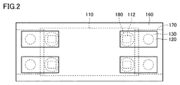
- FIG. 2 is a plan view of the magnetic sensor package of FIG. 1 as viewed from the direction of the arrow along line II-II.
- FIG. 3 is a bottom view of the magnetic sensor package of FIG. 1 as viewed from the direction of arrow III.
- the magnetic sensor package 100 includes a magnetic sensor chip 110, a connection wiring layer 120, a columnar electrode 130, an insulating layer 150, and a connection electrode 140. And.
- the magnetic sensor chip 110 has a rectangular parallelepiped shape.
- the magnetic sensor chip 110 has a first surface 111, a second surface 113 opposite to the first surface 111, and a peripheral surface connecting the first surface 111 and the second surface 113 to each other.
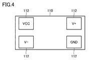
- FIG. 4 is a plan view showing the first surface of the magnetic sensor included in the magnetic sensor package according to the first embodiment of the present invention.
- four connection terminals 112 are provided on the first surface 111 of the magnetic sensor chip 110.
- the four connection terminals 112 are arranged one by one at the four corners of the first surface 111 of the magnetic sensor chip 110.
- the four connection terminals 112 are composed of a power supply terminal Vcc, a ground terminal GND, a first output terminal V +, and a second output terminal V-.
- the magnetic sensor chip 110 a magnetic detection element is arranged along the first surface 111.
- the magnetic sensor chip 110 includes a sensor substrate made of silicon, glass, ceramic, or the like, and a magnetic detection element and four connection terminals 112 are formed on the sensor substrate.
- the magnetic detection element is covered with a protective layer made of, for example, SiO 2 . An opening is formed in the protective layer of the portion located above each of the four connection terminals 112.
- the magnetic detection element is a TMR (Tunnel Magneto Resistance) element, but the magnetic detection element is not limited to the TMR element, and is an AMR (Anisotropic Magneto Resistance) element, a GMR (Giant Magneto Resistance) element, or the like. It may be a magnetoresistive element or a Hall element.
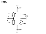
- FIG. 5 is a diagram showing a circuit configuration of a magnetic sensor chip included in the magnetic sensor package according to the first embodiment of the present invention.
- the magnetic sensor chip 110 has a Wheatstone bridge type bridge circuit including four TMR elements. Specifically, two series connectors of the variable resistor R1 and the fixed resistor R2 are connected in parallel between the power supply terminal Vcc and the ground terminal GND.
- the first output terminal V + is connected to the connection point between the fixed resistor R2 and the variable resistor R1.
- the second output terminal V- is connected to the connection point between the variable resistor R1 and the fixed resistor R2.
- the resistance value of the variable resistor R1 becomes smaller when the magnetic field to be detected acts on it.
- the resistance value of the fixed resistance R2 hardly decreases even when the magnetic field to be detected acts on it.
- the magnetic sensor chip 110 Since the magnetic sensor chip 110 has the above circuit configuration, a potential difference depending on the strength of the magnetic field to be detected is generated between the first output terminal V + and the second output terminal V-.
- the magnetic sensor chip 110 may have a half-bridge circuit including one variable resistor R1 and one fixed resistor R2.
- connection wiring layer 120 is electrically connected to the connection terminal 112, and is an edge of the magnetic sensor chip 110 along the first surface 111 and when viewed from a direction orthogonal to the first surface 111. It extends to the outside.
- the four connection wiring layers 120 are electrically connected to the four connection terminals 112 in a one-to-one correspondence.
- two of the four connection wiring layers 120 are orthogonal to one side of the edge of the magnetic sensor chip 110, and the remaining two are orthogonal to each other.
- the connection wiring layer 120 is orthogonal to the other side located parallel to the one side.
- connection wiring layer 120 has a rectangular parallelepiped shape.
- shape of the connection wiring layer 120 when viewed from a direction orthogonal to the first surface 111 is not limited to a rectangle, and may be an ellipse or the like.
- the connection wiring layer 120 is provided on the surface of the insulating layer 150 on the magnetic sensor chip side.
- the insulating layer 150 and the connecting wiring layer 120 are formed of a printed wiring board.
- connection wiring layer 120 The portion of the connection wiring layer 120 facing the connection terminal 112 is electrically connected to each other by the connection conductor 180.
- the connection wiring layer 120 is made of a conductive material such as gold or copper.
- the connecting conductor 180 is made of a conductive material such as solder or gold.
- the columnar electrode 130 is electrically connected to the connection wiring layer 120 at a position outside the edge of the magnetic sensor chip 110 when viewed from a direction orthogonal to the first surface 111, and the magnetic sensor is spaced apart from the magnetic sensor chip 110. It extends along the peripheral surface of the chip 110.
- the four columnar electrodes 130 are electrically connected to the four connection wiring layers 120 in a one-to-one correspondence.
- the columnar electrode 130 has a columnar shape.
- the shape of the columnar electrode 130 is not limited to the columnar shape, and may be a prismatic shape.
- the columnar electrode 130 is connected to the surface of the connection wiring layer 120 on the magnetic sensor chip side.
- the end surface of the columnar electrode 130 opposite to the connection wiring layer side is located on substantially the same plane as the second surface 113 of the magnetic sensor chip 110.
- the columnar electrode 130 is made of a conductive material such as gold or copper.
- the insulating layer 150 covers the first surface 111 of the magnetic sensor chip 110 while being in contact with the surface of the connection wiring layer 120 opposite to the surface on the magnetic sensor chip side.
- the surface of the insulating layer 150 on the magnetic sensor chip side and the first surface 111 face each other with a gap from each other.
- the thickness dimension of the insulating layer 150 is 20 ⁇ m or less.
- the portion located around the columnar electrode 130 is covered with the solder resist 170. That is, each part of the insulating layer 150 and the connecting wiring layer 120 is covered with the solder resist 170.
- the thickness dimension of the solder resist 170 is 20 ⁇ m or less.
- the distance between the surface of the insulating layer 150 opposite to the magnetic sensor chip side, which is the surface of the magnetic sensor package, and the magnetic detection element is 50 ⁇ m or less.
- the insulating layer 150 is formed of a glass epoxy substrate.
- the material constituting the insulating layer 150 is not limited to this, and may be a thermosetting resin such as an epoxy resin, a phenol resin, a melamine resin or a urethane resin, or a resin composition containing a thermosetting resin.
- connection electrode 140 is electrically connected to the end surface of the columnar electrode 130 opposite to the connection wiring layer side.
- the connection electrode 140 is made of a conductive material such as solder or gold.
- the magnetic sensor package 100 further includes a mold resin portion 160 that covers at least the peripheral surface of the magnetic sensor chip 110.
- the mold resin portion 160 fills a portion between the position on the surface of the insulating layer 150 on the magnetic sensor chip side and the position of the second surface 113 of the magnetic sensor chip 110 in the direction orthogonal to the first surface 111. ..
- the second surface 113 is a ground surface that has been ground.
- the end face of the columnar electrode 130 opposite to the connection wiring layer side is not covered with the mold resin portion 160.
- the mold resin portion 160 is made of a thermosetting molding material in which a silica filler or the like is added to a main component such as an epoxy resin.
- FIG. 6 is a vertical cross-sectional view showing a state in which a columnar electrode is formed on a printed wiring board in the method for manufacturing a magnetic sensor package according to the first embodiment of the present invention.
- a columnar electrode 130 is formed by plating on a printed wiring board including an insulating layer 150 and a connecting wiring layer 120.
- the columnar electrode 130 may be mounted on the connection wiring layer 120.
- the surface of the insulating layer 150 opposite to the connection wiring layer side is covered with the solder resist 190.
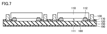
- FIG. 7 is a vertical sectional view showing a state in which a magnetic sensor chip is mounted on a printed wiring board in the method for manufacturing a magnetic sensor package according to the first embodiment of the present invention.
- the magnetic sensor chip 110 is flip-chip mounted on the printed wiring board so that the connection terminal 112 of the magnetic sensor chip 110 and the connection wiring layer 120 are electrically connected via the connection conductor 180. do.
- FIG. 8 is a vertical cross-sectional view showing a state in which a printed wiring board is resin-molded in the method for manufacturing a magnetic sensor package according to the first embodiment of the present invention. As shown in FIG. 8, the magnetic sensor chip 110 on the printed wiring board is embedded in the mold resin portion 160.
- FIG. 9 is a vertical sectional view showing a state in which the molded resin portion is ground together with the magnetic sensor chip and the columnar electrode in the method for manufacturing the magnetic sensor package according to the first embodiment of the present invention.
- the magnetic sensor is ground by grinding the mold resin portion 160 from the side opposite to the insulating layer side and also grinding the sides of the magnetic sensor chip 110 and the columnar electrode 130 opposite to the insulating layer side. Each of the second surface 113 of the chip 110 and the end face of the columnar electrode 130 opposite to the connection wiring layer side is exposed.
- FIG. 10 is a vertical cross-sectional view showing a state in which the insulating layer is ground in the method for manufacturing a magnetic sensor package according to the first embodiment of the present invention. As shown in FIG. 10, the solder resist 190 and the insulating layer 150 of the printed wiring board are ground to remove the solder resist 190 and thin the insulating layer 150.
- FIG. 11 is a vertical cross-sectional view showing a state in which a connection electrode is formed on an end surface of a columnar electrode opposite to the connection wiring layer side in the method for manufacturing a magnetic sensor package according to the first embodiment of the present invention.
- the connection electrode 140 is formed on the end surface of the columnar electrode 130 opposite to the connection wiring layer side by a plating method, a vapor deposition method, or a printing method.
- the magnetic sensor package 100 shown in FIG. 1 can be manufactured by individualizing it by dicing or the like.
- the magnetic sensor chip 110 has a first surface 111 provided with a connection terminal 112.
- a magnetic detection element is arranged along the first surface 111.
- the connection wiring layer 120 is electrically connected to the connection terminal 112 and extends along the first surface 111 to the outside of the edge of the magnetic sensor chip 110 when viewed from a direction orthogonal to the first surface 111.
- the columnar electrode 130 is electrically connected to the connection wiring layer 120 at a position outside the edge of the magnetic sensor chip 110 when viewed from a direction orthogonal to the first surface 111, and the magnetic sensor is spaced apart from the magnetic sensor chip 110. It extends along the chip 110.
- the insulating layer 150 covers the first surface 111 while being in contact with the surface of the connection wiring layer 120 opposite to the surface on the magnetic sensor chip side.
- the connection electrode 140 is electrically connected to the end surface of the columnar electrode 130 opposite to the connection wiring layer side.
- the magnetic detection element is arranged along the first surface 111 of the magnetic sensor chip 110.
- the distance from the surface of the magnetic sensor package 100 to the magnetic detection element is reduced to 50 ⁇ m or less, and the magnetic sensor package
- the magnetic detection accuracy for a magnetic field near the surface of 100 can be increased.
- connection electrode 140 which is a connection point with the substrate
- the stress transmission path to the detection element can be lengthened, and the stress transmitted to the magnetic detection element can be reduced to maintain high magnetic detection accuracy.
- the columnar electrode 130 is arranged outside the magnetic sensor chip 110, it is possible to suppress the magnetic field generated around the columnar electrode 130 due to the current flowing through the columnar electrode 130 from acting on the magnetic detection element. .. This also allows the magnetic sensor package 100 to maintain high magnetic detection accuracy.
- the insulating layer 150 and the connection wiring layer 120 are formed of a printed wiring board. This makes it possible to manufacture the magnetic sensor package 100 by a simple manufacturing method.
- the second surface 113 of the magnetic sensor chip 110 is a ground surface and is exposed from the mold resin portion 160. As a result, the magnetic sensor package 100 can be made thinner.
- the magnetic sensor package according to the second embodiment of the present invention is different from the magnetic sensor package 100 according to the first embodiment of the present invention in that the insulating layer is mainly composed of a thin film. The description of the configuration similar to that of the magnetic sensor package 100 according to the first embodiment will not be repeated.
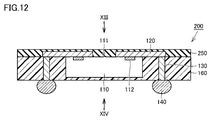
- FIG. 12 is a cross-sectional view showing the configuration of the magnetic sensor package according to the second embodiment of the present invention.
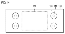
- FIG. 13 is a plan view of the magnetic sensor package of FIG. 12 as viewed from the direction of arrow XIII.
- FIG. 14 is a bottom view of the magnetic sensor package of FIG. 12 as viewed from the direction of arrow XIV. In FIG. 13, the insulating layer is shown through.
- the magnetic sensor package 200 includes a magnetic sensor chip 110, a connection wiring layer 120, a columnar electrode 130, an insulating layer 250, and a connection electrode 140. And.
- connection wiring layer 120 extends from the top of the first surface 111 of the magnetic sensor chip 110 to the outside of the edge of the magnetic sensor chip 110 along the first surface 111.
- the connection terminal 112 of the magnetic sensor chip 110 and the connection wiring layer 120 are directly connected to each other.
- the insulating layer 250 covers the first surface 111 of the magnetic sensor chip 110 while being in contact with the surface of the connection wiring layer 120 opposite to the surface on the magnetic sensor chip side.
- the insulating layer 250 covers the entire surface of the connection wiring layer 120 opposite to the surface on the magnetic sensor chip side.
- the surface of the insulating layer 250 on the magnetic sensor chip side and the first surface 111 are in direct contact with each other.
- the dimension of the thickness of the insulating layer 150 located on the first surface 111 is 10 ⁇ m or less.
- the distance between the surface of the insulating layer 250 opposite to the magnetic sensor chip side, which is the surface of the magnetic sensor package, and the magnetic detection element is 20 ⁇ m or less.
- the entire magnetic sensor chip 110 is embedded in the mold resin portion 160.
- FIG. 15 is a vertical sectional view showing a state in which a magnetic sensor chip and a columnar electrode are mounted on a support substrate provided with an adhesive sheet in the method for manufacturing a magnetic sensor package according to the second embodiment of the present invention.
- the magnetic sensor chip 110 and the columnar electrode 130 are mounted on the support substrate 290 provided with the adhesive sheet 291.
- the first surface 111 of the magnetic sensor chip 110 is in direct contact with the adhesive sheet 291.
- the columnar electrode 130 may be formed by plating on the adhesive sheet 291.
- FIG. 16 is a vertical sectional view showing a state in which a support substrate is resin-molded in the method for manufacturing a magnetic sensor package according to the first embodiment of the present invention.
- the magnetic sensor chip 110 and the columnar electrode 130 on the support substrate 290 are embedded in the mold resin portion 160.
- the end face of the columnar electrode 130 opposite to the support substrate side is exposed.
- the mold resin portion 160 may be molded so that the end face of the columnar electrode 130 is exposed, or the columnar electrode 130 may be molded so as to be embedded in the mold resin portion 160. After that, the end face of the columnar electrode 130 may be exposed by grinding the mold resin portion 160.
- FIG. 17 is a vertical sectional view showing a state in which a connection wiring layer and an insulating layer are formed after the adhesive sheet is peeled off and the support substrate is removed in the method for manufacturing a magnetic sensor package according to the second embodiment of the present invention. be.
- a film is formed by a sputtering method, a vapor deposition method, or the like, and the connection wiring layer 120 is formed by patterning by a photolithography method.
- the insulating layer 250 is formed by a sputtering method, a vapor deposition method, or the like so as to cover the first surface 111 of the magnetic sensor chip 110 and the connection wiring layer 120.
- the insulating layer 250 is made of SiO 2 or SiN or the like.
- FIG. 18 is a vertical cross-sectional view showing a state in which a connection electrode is formed on an end surface of a columnar electrode opposite to the connection wiring layer side in the method for manufacturing a magnetic sensor package according to the second embodiment of the present invention.
- the connection electrode 140 is formed on the end surface of the columnar electrode 130 on the side opposite to the connection wiring layer side by a plating method, a vapor deposition method, or a printing method.
- the magnetic sensor package 200 shown in FIG. 12 can be manufactured by individualizing it by dicing or the like.
- the insulating layer 250 is composed of a thin film having a thickness of 10 ⁇ m or less, the distance from the surface of the magnetic sensor package 100 to the magnetic detection element is 20 ⁇ m or less. The magnetic detection accuracy for the magnetic field near the surface of the magnetic sensor package 200 can be increased.
- connection electrode 140 which is a connection point with the substrate
- the stress transmission path to the detection element can be lengthened, and the stress transmitted to the magnetic detection element can be reduced to maintain high magnetic detection accuracy.
- the columnar electrode 130 is arranged outside the magnetic sensor chip 110, it is possible to suppress the magnetic field generated around the columnar electrode 130 due to the current flowing through the columnar electrode 130 from acting on the magnetic detection element. .. This also allows the magnetic sensor package 200 to maintain high magnetic detection accuracy.
- the magnetic sensor package according to the third embodiment of the present invention is different from the magnetic sensor package 200 according to the second embodiment of the present invention in that the second surface of the magnetic sensor chip is a ground surface.
- the description of the configuration similar to that of the magnetic sensor package 200 according to the second embodiment will not be repeated.
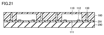
- FIG. 19 is a cross-sectional view showing the configuration of the magnetic sensor package according to the third embodiment of the present invention. As shown in FIG. 19, in the magnetic sensor package 300 according to the third embodiment of the present invention, only the second surface 113 is not covered with the mold resin portion 160 and is exposed. The second surface 113 is a ground surface that has been ground.
- FIG. 20 is a vertical sectional view showing a state in which a magnetic sensor chip and a columnar electrode are mounted on a support substrate provided with an adhesive sheet in the method for manufacturing a magnetic sensor package according to the third embodiment of the present invention.
- the magnetic sensor chip 110 and the columnar electrode 130 are mounted on the support substrate 290 provided with the adhesive sheet 291.
- the first surface 111 of the magnetic sensor chip 110 is in direct contact with the adhesive sheet 291.
- the columnar electrode 130 may be formed by plating on the adhesive sheet 291.
- FIG. 21 is a vertical sectional view showing a state in which a support substrate is resin-molded in the method for manufacturing a magnetic sensor package according to the third embodiment of the present invention. As shown in FIG. 21, the magnetic sensor chip 110 and the columnar electrode 130 on the support substrate 290 are embedded in the mold resin portion 160.
- FIG. 22 is a vertical sectional view showing a state in which the molded resin portion is ground together with the magnetic sensor chip and the columnar electrode in the method for manufacturing the magnetic sensor package according to the third embodiment of the present invention.
- the magnetic sensor is ground by grinding the mold resin portion 160 from the side opposite to the insulating layer side and also grinding the side opposite to the insulating layer side of each of the magnetic sensor chip 110 and the columnar electrode 130.
- Each of the second surface 113 of the chip 110 and the end face of the columnar electrode 130 opposite to the connection wiring layer side is exposed.
- FIG. 23 is a vertical sectional view showing a state in which a connection wiring layer and an insulating layer are formed after the adhesive sheet is peeled off and the support substrate is removed in the method for manufacturing a magnetic sensor package according to the third embodiment of the present invention. be.
- the connection wiring layer 120 is electrically connected to each of the connection terminal 112 and the columnar electrode 130 of the magnetic sensor chip 110.
- a film is formed by a sputtering method or a vapor deposition method, and patterning is performed by a photolithography method.
- the insulating layer 250 is formed by a sputtering method, a vapor deposition method, or the like so as to cover the first surface 111 of the magnetic sensor chip 110 and the connection wiring layer 120.
- FIG. 24 is a vertical cross-sectional view showing a state in which a connection electrode is formed on an end surface of a columnar electrode opposite to the connection wiring layer side in the method for manufacturing a magnetic sensor package according to the third embodiment of the present invention.
- the connection electrode 140 is formed on the end surface of the columnar electrode 130 opposite to the connection wiring layer side by a plating method, a vapor deposition method, or a printing method.
- the magnetic sensor package 300 shown in FIG. 19 can be manufactured by individualizing it by dicing or the like.
- the second surface 113 of the magnetic sensor chip 110 is a ground surface and is exposed from the mold resin portion 160. As a result, the magnetic sensor package 300 can be made thinner.
- the magnetic sensor package according to the fourth embodiment of the present invention is mainly the same as the magnetic sensor package 200 according to the second embodiment of the present invention in that an extension wiring layer is provided between the columnar electrode and the connection electrode. Since they are different, the description of the same configuration as that of the magnetic sensor package 200 according to the second embodiment of the present invention will not be repeated.
- FIG. 25 is a cross-sectional view showing the configuration of the magnetic sensor package according to the fourth embodiment of the present invention.
- FIG. 26 is a bottom view of the magnetic sensor package of FIG. 25 as viewed from the direction of arrow XXVI.
- the magnetic sensor package 400 includes a magnetic sensor chip 110, a connection wiring layer 120, a columnar electrode 130, an insulating layer 250, and a connection electrode 140. And an extension wiring layer 420.
- the extension wiring layer 420 is electrically connected to each of the end surface of the columnar electrode 130 opposite to the connection wiring layer side and the connection electrode 140, and is in a direction along the end surface of the columnar electrode 130 opposite to the connection wiring layer side. It is extended to.
- the extension wiring layer 420 extends along the surface of the mold resin portion 160 opposite to the insulating layer side.
- the columnar electrode 130 and the connection electrode 140 are electrically connected to each other via the extension wiring layer 420.
- FIG. 27 is a vertical sectional view showing a state in which a magnetic sensor chip and a columnar electrode are mounted on a support substrate provided with an adhesive sheet in the method for manufacturing a magnetic sensor package according to the fourth embodiment of the present invention.
- the magnetic sensor chip 110 and the columnar electrode 130 are mounted on the support substrate 290 provided with the adhesive sheet 291.
- the first surface 111 of the magnetic sensor chip 110 is in direct contact with the adhesive sheet 291.
- the columnar electrode 130 may be formed by plating on the adhesive sheet 291.
- FIG. 28 is a vertical cross-sectional view showing a state in which the support substrate is resin-molded in the method for manufacturing a magnetic sensor package according to the fourth embodiment of the present invention.
- the magnetic sensor chip 110 and the columnar electrode 130 on the support substrate 290 are embedded in the mold resin portion 160.
- the end face of the columnar electrode 130 opposite to the support substrate side is exposed.
- the entire magnetic sensor chip 110 is embedded in the mold resin portion 160.
- FIG. 29 is a vertical sectional view showing a state in which a connection wiring layer and an insulating layer are formed after the adhesive sheet is peeled off and the support substrate is removed in the method for manufacturing a magnetic sensor package according to the fourth embodiment of the present invention. be.
- the connection wiring layer 120 is electrically connected to each of the connection terminal 112 and the columnar electrode 130 of the magnetic sensor chip 110.
- a film is formed by a sputtering method or a vapor deposition method, and patterning is performed by a photolithography method.
- the insulating layer 250 is formed by a sputtering method, a vapor deposition method, or the like so as to cover the first surface 111 of the magnetic sensor chip 110 and the connection wiring layer 120.
- FIG. 30 is a vertical cross-sectional view showing a state in which an extension wiring layer is formed on an end surface of a columnar electrode opposite to the connection wiring layer side in the method for manufacturing a magnetic sensor package according to the fourth embodiment of the present invention. ..
- the extension wiring layer 420 is formed by forming a film by a sputtering method, a vapor deposition method, or the like so that the columnar electrode 130 and the extension wiring layer 420 are electrically connected, and patterning the extension wiring layer 420 by a photolithography method. Form.
- FIG. 31 is a vertical cross-sectional view showing a state in which a connection electrode is formed on an extension wiring layer in the method for manufacturing a magnetic sensor package according to the second embodiment of the present invention.
- the connection electrode 140 is formed on the extension wiring layer 420 by a plating method, a vapor deposition method, or a printing method.
- the magnetic sensor package 400 shown in FIG. 25 can be manufactured by individualizing it by dicing or the like.
- the end face of the columnar electrode 130 opposite to the connection wiring layer side and each of the connection electrodes 140 are electrically connected, and the connection wiring layer of the columnar electrode 130 is electrically connected. Further, an extension wiring layer 420 extending in a direction along the end face on the opposite side to the side is provided.
- connection electrode 140 which is a connection point with the substrate
- the stress transmission path from the connection electrode 140 to the magnetic detection element can be lengthened, and the stress transmitted to the magnetic detection element can be reduced to maintain high magnetic detection accuracy.
- connection electrode 140 since the columnar electrode 130 and the connection electrode 140 are electrically connected to each other via the extension wiring layer 420, the formation position of the connection electrode 140 can be adjusted according to the arrangement of the extension wiring layer 420. Therefore, the degree of freedom in the formation position of the connection electrode 140 can be increased.
- 100, 200, 300, 400 magnetic sensor package 110 magnetic sensor chip, 111 first surface, 112 connection terminal, 113 second surface, 120 connection wiring layer, 130 columnar electrode, 140 connection electrode, 150, 250 insulation layer, 160 Mold resin part, 170, 190 solder resist, 180 connection conductor, 290 support board, 291 adhesive sheet, 420 extension wiring layer, 2018 Japanese Patent Laid-Open No., GND ground terminal, R1 variable resistance, R2 fixed resistance, V + 1st output terminal, V -Second output terminal, Vcc power supply terminal.
Landscapes
- Physics & Mathematics (AREA)
- Condensed Matter Physics & Semiconductors (AREA)
- General Physics & Mathematics (AREA)
- Engineering & Computer Science (AREA)
- Computer Hardware Design (AREA)
- Microelectronics & Electronic Packaging (AREA)
- Power Engineering (AREA)
- Hall/Mr Elements (AREA)
- Measuring Magnetic Variables (AREA)
Abstract
A magnetism detection element is disposed along a first surface (111) of a magnetic sensor chip (110). A connection wiring layer (120) is electrically connected to a connection terminal (112) and extends along the first surface (111) and further outward than the edge of the magnetic sensor chip (110) in a view from a direction orthogonal to the first surface (111). A columnar electrode (130) is electrically connected to the connection wiring layer (120) at a position further outward than the edge of the magnetic sensor chip (110) in a view from a direction orthogonal to the first surface (111), is spaced apart from the magnetic sensor chip (110), and extends along the magnetic sensor chip (110). An insulating layer (150) is in contact with a surface of the connection wiring layer (120) on the opposite side from the magnetic sensor chip-side surface, and covers the first surface (111). A connection electrode (140) is electrically connected to an end face of the columnar electrode (130) on the opposite side from the connection wiring layer side.
Description
本発明は、磁気センサパッケージに関する。
The present invention relates to a magnetic sensor package.
パッケージングされた磁場センサの構成を開示した先行文献として、特開2018-119955号公報(特許文献1)がある。特許文献1に記載された磁場センサは、ダイの第1の表面内に配設された磁場感知素子と、ダイの第2の表面に接するはんだボールとを含む。シリコン貫通電極は、ダイを貫通して、磁場感知素子とはんだボールとを互いに接続している。
As a prior document disclosing the configuration of the packaged magnetic field sensor, there is Japanese Patent Application Laid-Open No. 2018-11995 (Patent Document 1). The magnetic field sensor described in Patent Document 1 includes a magnetic field sensing element disposed in the first surface of the die and a solder ball in contact with the second surface of the die. Through silicon vias penetrate the die to connect the magnetic field sensing element and the solder ball to each other.
特許文献1に記載された磁気センサパッケージにおいては、ダイの第1の表面内に磁気検出素子が配設されているため、磁気センサパッケージの表面から磁気検出素子までの距離を小さくして、磁気センサパッケージの表面近傍の磁界に対する磁気検出精度を高くできる可能性がある。
In the magnetic sensor package described in Patent Document 1, since the magnetic detection element is arranged in the first surface of the die, the distance from the surface of the magnetic sensor package to the magnetic detection element is reduced to reduce the magnetism. There is a possibility that the magnetic detection accuracy for the magnetic field near the surface of the sensor package can be improved.
磁気センサパッケージを基板に実装した際、磁気センサパッケージの構成部材同士の線膨張係数の違いによって磁気センサパッケージが撓むことにより応力が発生する。特許文献1に記載された磁気センサパッケージにおいては、はんだボールからシリコン貫通電極を通じて磁気検出素子に応力が伝達されるため、磁気検出素子までの応力伝達経路が短く、磁気検出素子に負荷される応力値が高くなり、磁気検出精度を高く維持することができない。
When the magnetic sensor package is mounted on the substrate, stress is generated due to the bending of the magnetic sensor package due to the difference in the linear expansion coefficient between the constituent members of the magnetic sensor package. In the magnetic sensor package described in Patent Document 1, since stress is transmitted from the solder ball to the magnetic detection element through the through silicon via, the stress transmission path to the magnetic detection element is short, and the stress applied to the magnetic detection element is short. The value becomes high, and the magnetic detection accuracy cannot be maintained high.
本発明は上記の問題点に鑑みてなされたものであって、基板に実装された際の基板との接続箇所から磁気検出素子に伝達される応力を低減して高い磁気検出精度を維持することができる、磁気センサパッケージを提供することを目的とする。
The present invention has been made in view of the above problems, and is to reduce the stress transmitted to the magnetic detection element from the connection point with the substrate when mounted on the substrate to maintain high magnetic detection accuracy. The purpose is to provide a magnetic sensor package that can be used.
本発明に基づく磁気センサパッケージは、磁気センサチップと、接続配線層と、柱状電極と、絶縁層と、接続電極とを備える。磁気センサチップは、接続端子が設けられた第1表面を有する。磁気センサチップにおいては、第1表面に沿って磁気検出素子が配置されている。接続配線層は、接続端子と電気的に接続され、上記第1表面に沿いつつ上記第1表面と直交する方向から見て磁気センサチップの縁より外側まで延在している。柱状電極は、上記第1表面と直交する方向から見て磁気センサチップの縁より外側の位置にて接続配線層と電気的に接続され、磁気センサチップに間隔をあけて磁気センサチップに沿って延在している。絶縁層は、接続配線層の磁気センサチップ側の面とは反対側の面と接しつつ、上記第1表面を覆っている。接続電極は、柱状電極の接続配線層側とは反対側の端面と電気的に接続されている。
The magnetic sensor package based on the present invention includes a magnetic sensor chip, a connection wiring layer, a columnar electrode, an insulating layer, and a connection electrode. The magnetic sensor chip has a first surface provided with connection terminals. In the magnetic sensor chip, a magnetic detection element is arranged along the first surface. The connection wiring layer is electrically connected to the connection terminal and extends along the first surface to the outside of the edge of the magnetic sensor chip when viewed from a direction orthogonal to the first surface. The columnar electrode is electrically connected to the connecting wiring layer at a position outside the edge of the magnetic sensor chip when viewed from the direction orthogonal to the first surface, and is spaced along the magnetic sensor chip along the magnetic sensor chip. It is postponed. The insulating layer covers the first surface while being in contact with the surface of the connection wiring layer opposite to the surface on the magnetic sensor chip side. The connection electrode is electrically connected to the end surface of the columnar electrode opposite to the connection wiring layer side.
本発明によれば、基板に実装された際の基板との接続箇所から磁気検出素子に伝達される応力を低減して高い磁気検出精度を維持することができる。
According to the present invention, it is possible to maintain high magnetic detection accuracy by reducing the stress transmitted to the magnetic detection element from the connection point with the board when mounted on the board.
以下、本発明の各実施の形態に係る磁気センサパッケージについて図を参照して説明する。以下の実施の形態の説明においては、図中の同一または相当部分には同一符号を付して、その説明は繰り返さない。
Hereinafter, the magnetic sensor package according to each embodiment of the present invention will be described with reference to the drawings. In the following description of the embodiment, the same or corresponding parts in the drawings are designated by the same reference numerals, and the description thereof will not be repeated.
(実施の形態1)
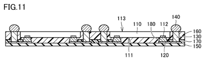
図1は、本発明の実施の形態1に係る磁気センサパッケージの構成を示す断面図である。図2は、図1の磁気センサパッケージをII-II線矢印方向から見た平面図である。図3は、図1の磁気センサパッケージを矢印III方向から見た底面図である。 (Embodiment 1)
FIG. 1 is a cross-sectional view showing the configuration of the magnetic sensor package according to the first embodiment of the present invention. FIG. 2 is a plan view of the magnetic sensor package of FIG. 1 as viewed from the direction of the arrow along line II-II. FIG. 3 is a bottom view of the magnetic sensor package of FIG. 1 as viewed from the direction of arrow III.
図1~図3に示すように、本発明の実施の形態1に係る磁気センサパッケージ100は、磁気センサチップ110と、接続配線層120と、柱状電極130と、絶縁層150と、接続電極140とを備える。
As shown in FIGS. 1 to 3, the magnetic sensor package 100 according to the first embodiment of the present invention includes a magnetic sensor chip 110, a connection wiring layer 120, a columnar electrode 130, an insulating layer 150, and a connection electrode 140. And.
磁気センサチップ110は、直方体状の形状を有している。磁気センサチップ110は、第1表面111、第1表面111とは反対側の第2表面113、および、第1表面111と第2表面113とを互いに接続する周面を有する。
The magnetic sensor chip 110 has a rectangular parallelepiped shape. The magnetic sensor chip 110 has a first surface 111, a second surface 113 opposite to the first surface 111, and a peripheral surface connecting the first surface 111 and the second surface 113 to each other.
図4は、本発明の実施の形態1に係る磁気センサパッケージが備える磁気センサの第1表面を示す平面図である。図4に示すように、磁気センサチップ110の第1表面111には、4つの接続端子112が設けられている。4つの接続端子112は、磁気センサチップ110の第1表面111の四隅に1つずつ配置されている。4つの接続端子112は、電源端子Vcc、接地端子GND、第1出力端子V+および第2出力端子V-から構成されている。
FIG. 4 is a plan view showing the first surface of the magnetic sensor included in the magnetic sensor package according to the first embodiment of the present invention. As shown in FIG. 4, four connection terminals 112 are provided on the first surface 111 of the magnetic sensor chip 110. The four connection terminals 112 are arranged one by one at the four corners of the first surface 111 of the magnetic sensor chip 110. The four connection terminals 112 are composed of a power supply terminal Vcc, a ground terminal GND, a first output terminal V +, and a second output terminal V-.
磁気センサチップ110においては、第1表面111に沿って磁気検出素子が配置されている。磁気センサチップ110は、シリコン、ガラスまたはセラミックなどで構成されたセンサ基板を含み、センサ基板上に磁気検出素子および4つの接続端子112が形成されている。磁気検出素子は、たとえばSiO2からなる保護層で覆われている。4つの接続端子112の各々の上方に位置する部分の保護層には、開口が形成されている。
In the magnetic sensor chip 110, a magnetic detection element is arranged along the first surface 111. The magnetic sensor chip 110 includes a sensor substrate made of silicon, glass, ceramic, or the like, and a magnetic detection element and four connection terminals 112 are formed on the sensor substrate. The magnetic detection element is covered with a protective layer made of, for example, SiO 2 . An opening is formed in the protective layer of the portion located above each of the four connection terminals 112.
本実施の形態においては、磁気検出素子は、TMR(Tunnel Magneto Resistance)素子であるが、磁気検出素子は、TMR素子に限られず、AMR(Anisotropic Magneto Resistance)素子またはGMR(Giant Magneto Resistance)素子などの磁気抵抗素子、またはホール素子であってもよい。
In the present embodiment, the magnetic detection element is a TMR (Tunnel Magneto Resistance) element, but the magnetic detection element is not limited to the TMR element, and is an AMR (Anisotropic Magneto Resistance) element, a GMR (Giant Magneto Resistance) element, or the like. It may be a magnetoresistive element or a Hall element.
図5は、本発明の実施の形態1に係る磁気センサパッケージが備える磁気センサチップの回路構成を示す図である。図5に示すように、磁気センサチップ110は、4つのTMR素子からなるホイートストンブリッジ型のブリッジ回路を有している。具体的には、可変抵抗R1と固定抵抗R2との2つの直列接続体が、電源端子Vccと接地端子GNDとの間に並列接続されている。一方の直列接続体においては、固定抵抗R2と可変抵抗R1との接続点に第1出力端子V+が接続されている。他方の直列接続体においては、可変抵抗R1と固定抵抗R2との接続点に第2出力端子V-が接続されている。可変抵抗R1は、検出対象磁界が作用すると、抵抗値が小さくなる。固定抵抗R2は、検出対象磁界が作用しても、抵抗値がほとんど低下しない。
FIG. 5 is a diagram showing a circuit configuration of a magnetic sensor chip included in the magnetic sensor package according to the first embodiment of the present invention. As shown in FIG. 5, the magnetic sensor chip 110 has a Wheatstone bridge type bridge circuit including four TMR elements. Specifically, two series connectors of the variable resistor R1 and the fixed resistor R2 are connected in parallel between the power supply terminal Vcc and the ground terminal GND. In one series connection body, the first output terminal V + is connected to the connection point between the fixed resistor R2 and the variable resistor R1. In the other series connection body, the second output terminal V- is connected to the connection point between the variable resistor R1 and the fixed resistor R2. The resistance value of the variable resistor R1 becomes smaller when the magnetic field to be detected acts on it. The resistance value of the fixed resistance R2 hardly decreases even when the magnetic field to be detected acts on it.
磁気センサチップ110が上記の回路構成を有することにより、第1出力端子V+と第2出力端子V-との間に、検出対象磁界の強さに依存する電位差が発生する。なお、磁気センサチップ110は、可変抵抗R1および固定抵抗R2を1つずつ含むハーフブリッジ回路を有していてもよい。
Since the magnetic sensor chip 110 has the above circuit configuration, a potential difference depending on the strength of the magnetic field to be detected is generated between the first output terminal V + and the second output terminal V-. The magnetic sensor chip 110 may have a half-bridge circuit including one variable resistor R1 and one fixed resistor R2.
図1および図2に示すように、接続配線層120は、接続端子112と電気的に接続され、第1表面111に沿いつつ第1表面111と直交する方向から見て磁気センサチップ110の縁より外側まで延在している。本実施の形態においては、4つの接続配線層120が、4つの接続端子112に1対1で対応して電気的に接続されている。第1表面111と直交する方向から見て、4つの接続配線層120のうちの2つの接続配線層120は、磁気センサチップ110の縁のうちの1辺と直交しており、残りの2つの接続配線層120は、上記1辺と平行に位置する他の1辺と直交している。
As shown in FIGS. 1 and 2, the connection wiring layer 120 is electrically connected to the connection terminal 112, and is an edge of the magnetic sensor chip 110 along the first surface 111 and when viewed from a direction orthogonal to the first surface 111. It extends to the outside. In this embodiment, the four connection wiring layers 120 are electrically connected to the four connection terminals 112 in a one-to-one correspondence. When viewed from a direction orthogonal to the first surface 111, two of the four connection wiring layers 120 are orthogonal to one side of the edge of the magnetic sensor chip 110, and the remaining two are orthogonal to each other. The connection wiring layer 120 is orthogonal to the other side located parallel to the one side.
具体的には、接続配線層120は、直方体状の形状を有している。ただし、第1表面111と直交する方向から見た接続配線層120の形状は、矩形に限られず、楕円形などであってもよい。接続配線層120は、絶縁層150の磁気センサチップ側の面上に設けられている。本実施の形態においては、絶縁層150および接続配線層120は、プリント配線板から形成されている。
Specifically, the connection wiring layer 120 has a rectangular parallelepiped shape. However, the shape of the connection wiring layer 120 when viewed from a direction orthogonal to the first surface 111 is not limited to a rectangle, and may be an ellipse or the like. The connection wiring layer 120 is provided on the surface of the insulating layer 150 on the magnetic sensor chip side. In the present embodiment, the insulating layer 150 and the connecting wiring layer 120 are formed of a printed wiring board.
接続配線層120における接続端子112と対向する部分は、接続導体180によって互いに電気的に接続されている。接続配線層120は、金または銅などの導電材料で構成されている。接続導体180は、はんだまたは金などの導電材料で構成されている。
The portion of the connection wiring layer 120 facing the connection terminal 112 is electrically connected to each other by the connection conductor 180. The connection wiring layer 120 is made of a conductive material such as gold or copper. The connecting conductor 180 is made of a conductive material such as solder or gold.
柱状電極130は、第1表面111と直交する方向から見て磁気センサチップ110の縁より外側の位置にて接続配線層120と電気的に接続され、磁気センサチップ110に間隔をあけて磁気センサチップ110の周面に沿って延在している。本実施の形態においては、4つの柱状電極130が、4つの接続配線層120に1対1で対応して電気的に接続されている。
The columnar electrode 130 is electrically connected to the connection wiring layer 120 at a position outside the edge of the magnetic sensor chip 110 when viewed from a direction orthogonal to the first surface 111, and the magnetic sensor is spaced apart from the magnetic sensor chip 110. It extends along the peripheral surface of the chip 110. In the present embodiment, the four columnar electrodes 130 are electrically connected to the four connection wiring layers 120 in a one-to-one correspondence.
具体的には、柱状電極130は、円柱状の形状を有している。ただし、柱状電極130の形状は、円柱状に限られず、角柱状でもよい。柱状電極130は、接続配線層120の磁気センサチップ側の面に接続されている。柱状電極130の接続配線層側とは反対側の端面は、磁気センサチップ110の第2表面113と略同一平面上に位置している。柱状電極130は、金または銅などの導電材料で構成されている。
Specifically, the columnar electrode 130 has a columnar shape. However, the shape of the columnar electrode 130 is not limited to the columnar shape, and may be a prismatic shape. The columnar electrode 130 is connected to the surface of the connection wiring layer 120 on the magnetic sensor chip side. The end surface of the columnar electrode 130 opposite to the connection wiring layer side is located on substantially the same plane as the second surface 113 of the magnetic sensor chip 110. The columnar electrode 130 is made of a conductive material such as gold or copper.
絶縁層150は、接続配線層120の磁気センサチップ側の面とは反対側の面と接しつつ、磁気センサチップ110の第1表面111を覆っている。絶縁層150の磁気センサチップ側の面と第1表面111とは、互いに間隔をあけて対向している。絶縁層150の厚みの寸法は、20μm以下である。
The insulating layer 150 covers the first surface 111 of the magnetic sensor chip 110 while being in contact with the surface of the connection wiring layer 120 opposite to the surface on the magnetic sensor chip side. The surface of the insulating layer 150 on the magnetic sensor chip side and the first surface 111 face each other with a gap from each other. The thickness dimension of the insulating layer 150 is 20 μm or less.
プリント配線板において、柱状電極130の周囲に位置する部分は、ソルダーレジスト170によって覆われている。すなわち、絶縁層150および接続配線層120の各々の一部は、ソルダーレジスト170によって覆われている。ソルダーレジスト170の厚みの寸法は、20μm以下である。
In the printed wiring board, the portion located around the columnar electrode 130 is covered with the solder resist 170. That is, each part of the insulating layer 150 and the connecting wiring layer 120 is covered with the solder resist 170. The thickness dimension of the solder resist 170 is 20 μm or less.
磁気センサパッケージの表面となる、絶縁層150の磁気センサチップ側とは反対側の面と、磁気検出素子との間隔は、50μm以下である。
The distance between the surface of the insulating layer 150 opposite to the magnetic sensor chip side, which is the surface of the magnetic sensor package, and the magnetic detection element is 50 μm or less.
絶縁層150は、ガラスエポキシ基板から形成されている。ただし、絶縁層150を構成する材料は、これに限られず、エポキシ樹脂、フェノール樹脂、メラミン樹脂またはウレタン樹脂などの熱硬化性樹脂、もしくは熱硬化性樹脂を含む樹脂組成物であってもよい。
The insulating layer 150 is formed of a glass epoxy substrate. However, the material constituting the insulating layer 150 is not limited to this, and may be a thermosetting resin such as an epoxy resin, a phenol resin, a melamine resin or a urethane resin, or a resin composition containing a thermosetting resin.
接続電極140は、柱状電極130の接続配線層側とは反対側の端面と電気的に接続されている。接続電極140は、はんだまたは金などの導電材料で構成されている。
The connection electrode 140 is electrically connected to the end surface of the columnar electrode 130 opposite to the connection wiring layer side. The connection electrode 140 is made of a conductive material such as solder or gold.
磁気センサパッケージ100は、磁気センサチップ110の少なくとも周面を覆うモールド樹脂部160をさらに備えている。モールド樹脂部160は、第1表面111と直交する方向における、絶縁層150の磁気センサチップ側の面上の位置から磁気センサチップ110の第2表面113の位置までの間の部分を埋めている。磁気センサチップ110においては、第2表面113のみモールド樹脂部160に覆われておらず露出している。第2表面113は、研削された研削面である。柱状電極130の接続配線層側とは反対側の端面は、モールド樹脂部160に覆われていない。モールド樹脂部160は、たとえばエポキシ樹脂などの主成分にシリカ充填材などが加えられた熱硬化性成形材料で構成されている。
The magnetic sensor package 100 further includes a mold resin portion 160 that covers at least the peripheral surface of the magnetic sensor chip 110. The mold resin portion 160 fills a portion between the position on the surface of the insulating layer 150 on the magnetic sensor chip side and the position of the second surface 113 of the magnetic sensor chip 110 in the direction orthogonal to the first surface 111. .. In the magnetic sensor chip 110, only the second surface 113 is not covered with the mold resin portion 160 and is exposed. The second surface 113 is a ground surface that has been ground. The end face of the columnar electrode 130 opposite to the connection wiring layer side is not covered with the mold resin portion 160. The mold resin portion 160 is made of a thermosetting molding material in which a silica filler or the like is added to a main component such as an epoxy resin.
以下、本発明の実施の形態1に係る磁気センサパッケージ100の製造方法について説明する。
Hereinafter, a method for manufacturing the magnetic sensor package 100 according to the first embodiment of the present invention will be described.
図6は、本発明の実施の形態1に係る磁気センサパッケージの製造方法において、プリント配線板上に柱状電極を形成した状態を示す縦断面図である。図6に示すように、絶縁層150および接続配線層120を含むプリント配線板上に、めっきによって柱状電極130を形成する。なお、柱状電極130は、接続配線層120上に実装されてもよい。絶縁層150の接続配線層側とは反対側の面は、ソルダーレジスト190に覆われている。
FIG. 6 is a vertical cross-sectional view showing a state in which a columnar electrode is formed on a printed wiring board in the method for manufacturing a magnetic sensor package according to the first embodiment of the present invention. As shown in FIG. 6, a columnar electrode 130 is formed by plating on a printed wiring board including an insulating layer 150 and a connecting wiring layer 120. The columnar electrode 130 may be mounted on the connection wiring layer 120. The surface of the insulating layer 150 opposite to the connection wiring layer side is covered with the solder resist 190.
図7は、本発明の実施の形態1に係る磁気センサパッケージの製造方法において、プリント配線板上に磁気センサチップを実装した状態を示す縦断面図である。図7に示すように、磁気センサチップ110の接続端子112と接続配線層120とが接続導体180を介して電気的に接続されるように、プリント配線板上に磁気センサチップ110をフリップチップ実装する。
FIG. 7 is a vertical sectional view showing a state in which a magnetic sensor chip is mounted on a printed wiring board in the method for manufacturing a magnetic sensor package according to the first embodiment of the present invention. As shown in FIG. 7, the magnetic sensor chip 110 is flip-chip mounted on the printed wiring board so that the connection terminal 112 of the magnetic sensor chip 110 and the connection wiring layer 120 are electrically connected via the connection conductor 180. do.
図8は、本発明の実施の形態1に係る磁気センサパッケージの製造方法において、プリント配線板上を樹脂モールドした状態を示す縦断面図である。図8に示すように、プリント配線板上の磁気センサチップ110をモールド樹脂部160内に埋め込む。
FIG. 8 is a vertical cross-sectional view showing a state in which a printed wiring board is resin-molded in the method for manufacturing a magnetic sensor package according to the first embodiment of the present invention. As shown in FIG. 8, the magnetic sensor chip 110 on the printed wiring board is embedded in the mold resin portion 160.
図9は、本発明の実施の形態1に係る磁気センサパッケージの製造方法において、モールド樹脂部を磁気センサチップおよび柱状電極とともに研削した状態を示す縦断面図である。図9に示すように、モールド樹脂部160を絶縁層側とは反対側から研削するとともに、磁気センサチップ110および柱状電極130の各々の絶縁層側とは反対側も研削することにより、磁気センサチップ110の第2表面113および柱状電極130の接続配線層側とは反対側の端面の各々を露出させる。
FIG. 9 is a vertical sectional view showing a state in which the molded resin portion is ground together with the magnetic sensor chip and the columnar electrode in the method for manufacturing the magnetic sensor package according to the first embodiment of the present invention. As shown in FIG. 9, the magnetic sensor is ground by grinding the mold resin portion 160 from the side opposite to the insulating layer side and also grinding the sides of the magnetic sensor chip 110 and the columnar electrode 130 opposite to the insulating layer side. Each of the second surface 113 of the chip 110 and the end face of the columnar electrode 130 opposite to the connection wiring layer side is exposed.
図10は、本発明の実施の形態1に係る磁気センサパッケージの製造方法において、絶縁層を研削した状態を示す縦断面図である。図10に示すように、プリント配線板のソルダーレジスト190および絶縁層150を研削して、ソルダーレジスト190を除去するとともに絶縁層150を薄くする。
FIG. 10 is a vertical cross-sectional view showing a state in which the insulating layer is ground in the method for manufacturing a magnetic sensor package according to the first embodiment of the present invention. As shown in FIG. 10, the solder resist 190 and the insulating layer 150 of the printed wiring board are ground to remove the solder resist 190 and thin the insulating layer 150.
図11は、本発明の実施の形態1に係る磁気センサパッケージの製造方法において、柱状電極の接続配線層側とは反対側の端面上に接続電極を形成した状態を示す縦断面図である。図11に示すように、柱状電極130の接続配線層側とは反対側の端面上に、めっき法、蒸着法または印刷法によって、接続電極140を形成する。最後にダイシングなどによって個片化することにより、図1に示す磁気センサパッケージ100を製造することができる。
FIG. 11 is a vertical cross-sectional view showing a state in which a connection electrode is formed on an end surface of a columnar electrode opposite to the connection wiring layer side in the method for manufacturing a magnetic sensor package according to the first embodiment of the present invention. As shown in FIG. 11, the connection electrode 140 is formed on the end surface of the columnar electrode 130 opposite to the connection wiring layer side by a plating method, a vapor deposition method, or a printing method. Finally, the magnetic sensor package 100 shown in FIG. 1 can be manufactured by individualizing it by dicing or the like.
本発明の実施の形態1に係る磁気センサパッケージ100においては、磁気センサチップ110は、接続端子112が設けられた第1表面111を有する。磁気センサチップ110においては、第1表面111に沿って磁気検出素子が配置されている。接続配線層120は、接続端子112と電気的に接続され、第1表面111に沿いつつ第1表面111と直交する方向から見て磁気センサチップ110の縁より外側まで延在している。柱状電極130は、第1表面111と直交する方向から見て磁気センサチップ110の縁より外側の位置にて接続配線層120と電気的に接続され、磁気センサチップ110に間隔をあけて磁気センサチップ110に沿って延在している。絶縁層150は、接続配線層120の磁気センサチップ側の面とは反対側の面と接しつつ、第1表面111を覆っている。接続電極140は、柱状電極130の接続配線層側とは反対側の端面と電気的に接続されている。
In the magnetic sensor package 100 according to the first embodiment of the present invention, the magnetic sensor chip 110 has a first surface 111 provided with a connection terminal 112. In the magnetic sensor chip 110, a magnetic detection element is arranged along the first surface 111. The connection wiring layer 120 is electrically connected to the connection terminal 112 and extends along the first surface 111 to the outside of the edge of the magnetic sensor chip 110 when viewed from a direction orthogonal to the first surface 111. The columnar electrode 130 is electrically connected to the connection wiring layer 120 at a position outside the edge of the magnetic sensor chip 110 when viewed from a direction orthogonal to the first surface 111, and the magnetic sensor is spaced apart from the magnetic sensor chip 110. It extends along the chip 110. The insulating layer 150 covers the first surface 111 while being in contact with the surface of the connection wiring layer 120 opposite to the surface on the magnetic sensor chip side. The connection electrode 140 is electrically connected to the end surface of the columnar electrode 130 opposite to the connection wiring layer side.
磁気センサチップ110の第1表面111に沿って磁気検出素子が配置されており、上記の構成により、磁気センサパッケージ100の表面から磁気検出素子までの間隔を50μm以下まで小さくして、磁気センサパッケージ100の表面近傍の磁界に対する磁気検出精度を高くできる。
The magnetic detection element is arranged along the first surface 111 of the magnetic sensor chip 110. With the above configuration, the distance from the surface of the magnetic sensor package 100 to the magnetic detection element is reduced to 50 μm or less, and the magnetic sensor package The magnetic detection accuracy for a magnetic field near the surface of 100 can be increased.
また、磁気センサパッケージ100が基板に実装された際、基板との接続箇所である接続電極140から柱状電極130および接続配線層120を通じて磁気検出素子に応力が伝達されるため、接続電極140から磁気検出素子までの応力の伝達経路を長くすることができ、ひいては、磁気検出素子に伝達される応力を低減して高い磁気検出精度を維持することができる。
Further, when the magnetic sensor package 100 is mounted on the substrate, stress is transmitted from the connection electrode 140, which is a connection point with the substrate, to the magnetic detection element through the columnar electrode 130 and the connection wiring layer 120, so that the magnetic sensor package 100 is magnetic from the connection electrode 140. The stress transmission path to the detection element can be lengthened, and the stress transmitted to the magnetic detection element can be reduced to maintain high magnetic detection accuracy.
さらに、柱状電極130を磁気センサチップ110の外側に配置しているため、柱状電極130を流れる電流によって柱状電極130の周囲に発生する磁界が、磁気検出素子に作用することを抑制することができる。これによっても、磁気センサパッケージ100は、高い磁気検出精度を維持することができる。
Further, since the columnar electrode 130 is arranged outside the magnetic sensor chip 110, it is possible to suppress the magnetic field generated around the columnar electrode 130 due to the current flowing through the columnar electrode 130 from acting on the magnetic detection element. .. This also allows the magnetic sensor package 100 to maintain high magnetic detection accuracy.
本発明の実施の形態1に係る磁気センサパッケージ100においては、絶縁層150および接続配線層120は、プリント配線板から形成されている。これにより、簡易な製造方法によって磁気センサパッケージ100を製造することが可能となる。
In the magnetic sensor package 100 according to the first embodiment of the present invention, the insulating layer 150 and the connection wiring layer 120 are formed of a printed wiring board. This makes it possible to manufacture the magnetic sensor package 100 by a simple manufacturing method.
本発明の実施の形態1に係る磁気センサパッケージ100においては、磁気センサチップ110の第2表面113は、研削面であり、モールド樹脂部160から露出している。これにより、磁気センサパッケージ100を薄型化することができる。
In the magnetic sensor package 100 according to the first embodiment of the present invention, the second surface 113 of the magnetic sensor chip 110 is a ground surface and is exposed from the mold resin portion 160. As a result, the magnetic sensor package 100 can be made thinner.
(実施の形態2)
以下、本発明の実施の形態2に係る磁気センサパッケージについて図を参照して説明する。本発明の実施の形態2に係る磁気センサパッケージは、絶縁層が薄膜で構成されている点が主に、本発明の実施の形態1に係る磁気センサパッケージ100と異なるため、本発明の実施の形態1に係る磁気センサパッケージ100と同様である構成については説明を繰り返さない。 (Embodiment 2)
Hereinafter, the magnetic sensor package according to the second embodiment of the present invention will be described with reference to the drawings. The magnetic sensor package according to the second embodiment of the present invention is different from themagnetic sensor package 100 according to the first embodiment of the present invention in that the insulating layer is mainly composed of a thin film. The description of the configuration similar to that of the magnetic sensor package 100 according to the first embodiment will not be repeated.
以下、本発明の実施の形態2に係る磁気センサパッケージについて図を参照して説明する。本発明の実施の形態2に係る磁気センサパッケージは、絶縁層が薄膜で構成されている点が主に、本発明の実施の形態1に係る磁気センサパッケージ100と異なるため、本発明の実施の形態1に係る磁気センサパッケージ100と同様である構成については説明を繰り返さない。 (Embodiment 2)
Hereinafter, the magnetic sensor package according to the second embodiment of the present invention will be described with reference to the drawings. The magnetic sensor package according to the second embodiment of the present invention is different from the
図12は、本発明の実施の形態2に係る磁気センサパッケージの構成を示す断面図である。図13は、図12の磁気センサパッケージを矢印XIII方向から見た平面図である。図14は、図12の磁気センサパッケージを矢印XIV方向から見た底面図である。図13においては、絶縁層を透視して図示している。
FIG. 12 is a cross-sectional view showing the configuration of the magnetic sensor package according to the second embodiment of the present invention. FIG. 13 is a plan view of the magnetic sensor package of FIG. 12 as viewed from the direction of arrow XIII. FIG. 14 is a bottom view of the magnetic sensor package of FIG. 12 as viewed from the direction of arrow XIV. In FIG. 13, the insulating layer is shown through.
図12~図14に示すように、本発明の実施の形態2に係る磁気センサパッケージ200は、磁気センサチップ110と、接続配線層120と、柱状電極130と、絶縁層250と、接続電極140とを備える。
As shown in FIGS. 12 to 14, the magnetic sensor package 200 according to the second embodiment of the present invention includes a magnetic sensor chip 110, a connection wiring layer 120, a columnar electrode 130, an insulating layer 250, and a connection electrode 140. And.
接続配線層120は、磁気センサチップ110の第1表面111上から第1表面111に沿いつつ磁気センサチップ110の縁の外側まで延在している。磁気センサチップ110の接続端子112と接続配線層120とは、互いに直接接続されている。
The connection wiring layer 120 extends from the top of the first surface 111 of the magnetic sensor chip 110 to the outside of the edge of the magnetic sensor chip 110 along the first surface 111. The connection terminal 112 of the magnetic sensor chip 110 and the connection wiring layer 120 are directly connected to each other.
絶縁層250は、接続配線層120の磁気センサチップ側の面とは反対側の面と接しつつ、磁気センサチップ110の第1表面111を覆っている。絶縁層250は、接続配線層120の磁気センサチップ側の面とは反対側の面の全体を覆っている。絶縁層250の磁気センサチップ側の面と第1表面111とは、互いに直接接触している。第1表面111上に位置する絶縁層150の厚みの寸法は、10μm以下である。
The insulating layer 250 covers the first surface 111 of the magnetic sensor chip 110 while being in contact with the surface of the connection wiring layer 120 opposite to the surface on the magnetic sensor chip side. The insulating layer 250 covers the entire surface of the connection wiring layer 120 opposite to the surface on the magnetic sensor chip side. The surface of the insulating layer 250 on the magnetic sensor chip side and the first surface 111 are in direct contact with each other. The dimension of the thickness of the insulating layer 150 located on the first surface 111 is 10 μm or less.
磁気センサパッケージの表面となる、絶縁層250の磁気センサチップ側とは反対側の面と、磁気検出素子との間隔は、20μm以下である。本実施の形態においては、磁気センサチップ110の全体が、モールド樹脂部160に埋め込まれている。
The distance between the surface of the insulating layer 250 opposite to the magnetic sensor chip side, which is the surface of the magnetic sensor package, and the magnetic detection element is 20 μm or less. In the present embodiment, the entire magnetic sensor chip 110 is embedded in the mold resin portion 160.
以下、本発明の実施の形態2に係る磁気センサパッケージ200の製造方法について説明する。
Hereinafter, a method for manufacturing the magnetic sensor package 200 according to the second embodiment of the present invention will be described.
図15は、本発明の実施の形態2に係る磁気センサパッケージの製造方法において、接着シートが設けられた支持基板上に磁気センサチップおよび柱状電極を実装した状態を示す縦断面図である。図15に示すように、接着シート291が設けられた支持基板290上に磁気センサチップ110および柱状電極130を実装する。磁気センサチップ110の第1表面111は、接着シート291と直接接触している。なお、柱状電極130は、接着シート291上にめっきすることで形成してもよい。
FIG. 15 is a vertical sectional view showing a state in which a magnetic sensor chip and a columnar electrode are mounted on a support substrate provided with an adhesive sheet in the method for manufacturing a magnetic sensor package according to the second embodiment of the present invention. As shown in FIG. 15, the magnetic sensor chip 110 and the columnar electrode 130 are mounted on the support substrate 290 provided with the adhesive sheet 291. The first surface 111 of the magnetic sensor chip 110 is in direct contact with the adhesive sheet 291. The columnar electrode 130 may be formed by plating on the adhesive sheet 291.
図16は、本発明の実施の形態1に係る磁気センサパッケージの製造方法において、支持基板上を樹脂モールドした状態を示す縦断面図である。図16に示すように、支持基板290上の磁気センサチップ110および柱状電極130をモールド樹脂部160内に埋め込む。柱状電極130の支持基板側とは反対側の端面は、露出している。柱状電極130の端面を露出させる方法として、柱状電極130の端面が露出する厚みとなるようにモールド樹脂部160を成型してもよいし、柱状電極130がモールド樹脂部160に埋め込まれるように成型した後、モールド樹脂部160を研削することにより、柱状電極130の端面を露出させてもよい。
FIG. 16 is a vertical sectional view showing a state in which a support substrate is resin-molded in the method for manufacturing a magnetic sensor package according to the first embodiment of the present invention. As shown in FIG. 16, the magnetic sensor chip 110 and the columnar electrode 130 on the support substrate 290 are embedded in the mold resin portion 160. The end face of the columnar electrode 130 opposite to the support substrate side is exposed. As a method of exposing the end face of the columnar electrode 130, the mold resin portion 160 may be molded so that the end face of the columnar electrode 130 is exposed, or the columnar electrode 130 may be molded so as to be embedded in the mold resin portion 160. After that, the end face of the columnar electrode 130 may be exposed by grinding the mold resin portion 160.
図17は、本発明の実施の形態2に係る磁気センサパッケージの製造方法において、接着シートを剥離させて支持基板を取り外した後、接続配線層および絶縁層を形成した状態を示す縦断面図である。図17に示すように、接着シート291を剥離させて支持基板290を取り外した後、磁気センサチップ110の接続端子112および柱状電極130の各々と接続配線層120が電気的に接続されるように、スパッタリング法または蒸着法などによって成膜し、フォトリソグラフィ法によってパターニングすることにより、接続配線層120を形成する。さらに、磁気センサチップ110の第1表面111および接続配線層120を覆うように絶縁層250をスパッタリング法または蒸着法などによって成膜する。絶縁層250は、SiO2またはSiNなどで構成されている。
FIG. 17 is a vertical sectional view showing a state in which a connection wiring layer and an insulating layer are formed after the adhesive sheet is peeled off and the support substrate is removed in the method for manufacturing a magnetic sensor package according to the second embodiment of the present invention. be. As shown in FIG. 17, after the adhesive sheet 291 is peeled off and the support substrate 290 is removed, each of the connection terminal 112 and the columnar electrode 130 of the magnetic sensor chip 110 is electrically connected to the connection wiring layer 120. , A film is formed by a sputtering method, a vapor deposition method, or the like, and the connection wiring layer 120 is formed by patterning by a photolithography method. Further, the insulating layer 250 is formed by a sputtering method, a vapor deposition method, or the like so as to cover the first surface 111 of the magnetic sensor chip 110 and the connection wiring layer 120. The insulating layer 250 is made of SiO 2 or SiN or the like.
図18は、本発明の実施の形態2に係る磁気センサパッケージの製造方法において、柱状電極の接続配線層側とは反対側の端面上に接続電極を形成した状態を示す縦断面図である。図18に示すように、柱状電極130の接続配線層側とは反対側の端面上に、めっき法、蒸着法または印刷法によって、接続電極140を形成する。最後にダイシングなどによって個片化することにより、図12に示す磁気センサパッケージ200を製造することができる。
FIG. 18 is a vertical cross-sectional view showing a state in which a connection electrode is formed on an end surface of a columnar electrode opposite to the connection wiring layer side in the method for manufacturing a magnetic sensor package according to the second embodiment of the present invention. As shown in FIG. 18, the connection electrode 140 is formed on the end surface of the columnar electrode 130 on the side opposite to the connection wiring layer side by a plating method, a vapor deposition method, or a printing method. Finally, the magnetic sensor package 200 shown in FIG. 12 can be manufactured by individualizing it by dicing or the like.
本発明の実施の形態2に係る磁気センサパッケージ200においては、絶縁層250は、厚みが10μm以下の薄膜で構成されているため、磁気センサパッケージ100の表面から磁気検出素子までの間隔を20μm以下まで小さくして、磁気センサパッケージ200の表面近傍の磁界に対する磁気検出精度を高くできる。
In the magnetic sensor package 200 according to the second embodiment of the present invention, since the insulating layer 250 is composed of a thin film having a thickness of 10 μm or less, the distance from the surface of the magnetic sensor package 100 to the magnetic detection element is 20 μm or less. The magnetic detection accuracy for the magnetic field near the surface of the magnetic sensor package 200 can be increased.
また、磁気センサパッケージ200が基板に実装された際、基板との接続箇所である接続電極140から柱状電極130および接続配線層120を通じて磁気検出素子に応力が伝達されるため、接続電極140から磁気検出素子までの応力の伝達経路を長くすることができ、ひいては、磁気検出素子に伝達される応力を低減して高い磁気検出精度を維持することができる。
Further, when the magnetic sensor package 200 is mounted on the substrate, stress is transmitted from the connection electrode 140, which is a connection point with the substrate, to the magnetic detection element through the columnar electrode 130 and the connection wiring layer 120, so that the magnetic sensor package 200 is magnetic from the connection electrode 140. The stress transmission path to the detection element can be lengthened, and the stress transmitted to the magnetic detection element can be reduced to maintain high magnetic detection accuracy.
さらに、柱状電極130を磁気センサチップ110の外側に配置しているため、柱状電極130を流れる電流によって柱状電極130の周囲に発生する磁界が、磁気検出素子に作用することを抑制することができる。これによっても、磁気センサパッケージ200は、高い磁気検出精度を維持することができる。
Further, since the columnar electrode 130 is arranged outside the magnetic sensor chip 110, it is possible to suppress the magnetic field generated around the columnar electrode 130 due to the current flowing through the columnar electrode 130 from acting on the magnetic detection element. .. This also allows the magnetic sensor package 200 to maintain high magnetic detection accuracy.
(実施の形態3)
以下、本発明の実施の形態3に係る磁気センサパッケージについて図を参照して説明する。本発明の実施の形態3に係る磁気センサパッケージは、磁気センサチップの第2表面が研削面である点が、本発明の実施の形態2に係る磁気センサパッケージ200と異なるため、本発明の実施の形態2に係る磁気センサパッケージ200と同様である構成については説明を繰り返さない。 (Embodiment 3)
Hereinafter, the magnetic sensor package according to the third embodiment of the present invention will be described with reference to the drawings. The magnetic sensor package according to the third embodiment of the present invention is different from themagnetic sensor package 200 according to the second embodiment of the present invention in that the second surface of the magnetic sensor chip is a ground surface. The description of the configuration similar to that of the magnetic sensor package 200 according to the second embodiment will not be repeated.
以下、本発明の実施の形態3に係る磁気センサパッケージについて図を参照して説明する。本発明の実施の形態3に係る磁気センサパッケージは、磁気センサチップの第2表面が研削面である点が、本発明の実施の形態2に係る磁気センサパッケージ200と異なるため、本発明の実施の形態2に係る磁気センサパッケージ200と同様である構成については説明を繰り返さない。 (Embodiment 3)
Hereinafter, the magnetic sensor package according to the third embodiment of the present invention will be described with reference to the drawings. The magnetic sensor package according to the third embodiment of the present invention is different from the
図19は、本発明の実施の形態3に係る磁気センサパッケージの構成を示す断面図である。図19に示すように、本発明の実施の形態3に係る磁気センサパッケージ300においては、第2表面113のみモールド樹脂部160に覆われておらず露出している。第2表面113は、研削された研削面である。
FIG. 19 is a cross-sectional view showing the configuration of the magnetic sensor package according to the third embodiment of the present invention. As shown in FIG. 19, in the magnetic sensor package 300 according to the third embodiment of the present invention, only the second surface 113 is not covered with the mold resin portion 160 and is exposed. The second surface 113 is a ground surface that has been ground.
以下、本発明の実施の形態3に係る磁気センサパッケージ300の製造方法について説明する。
Hereinafter, a method for manufacturing the magnetic sensor package 300 according to the third embodiment of the present invention will be described.
図20は、本発明の実施の形態3に係る磁気センサパッケージの製造方法において、接着シートが設けられた支持基板上に磁気センサチップおよび柱状電極を実装した状態を示す縦断面図である。図20に示すように、接着シート291が設けられた支持基板290上に磁気センサチップ110および柱状電極130を実装する。磁気センサチップ110の第1表面111は、接着シート291と直接接触している。なお、柱状電極130は、接着シート291上にめっきすることで形成してもよい。
FIG. 20 is a vertical sectional view showing a state in which a magnetic sensor chip and a columnar electrode are mounted on a support substrate provided with an adhesive sheet in the method for manufacturing a magnetic sensor package according to the third embodiment of the present invention. As shown in FIG. 20, the magnetic sensor chip 110 and the columnar electrode 130 are mounted on the support substrate 290 provided with the adhesive sheet 291. The first surface 111 of the magnetic sensor chip 110 is in direct contact with the adhesive sheet 291. The columnar electrode 130 may be formed by plating on the adhesive sheet 291.
図21は、本発明の実施の形態3に係る磁気センサパッケージの製造方法において、支持基板上を樹脂モールドした状態を示す縦断面図である。図21に示すように、支持基板290上の磁気センサチップ110および柱状電極130をモールド樹脂部160内に埋め込む。
FIG. 21 is a vertical sectional view showing a state in which a support substrate is resin-molded in the method for manufacturing a magnetic sensor package according to the third embodiment of the present invention. As shown in FIG. 21, the magnetic sensor chip 110 and the columnar electrode 130 on the support substrate 290 are embedded in the mold resin portion 160.
図22は、本発明の実施の形態3に係る磁気センサパッケージの製造方法において、モールド樹脂部を磁気センサチップおよび柱状電極とともに研削した状態を示す縦断面図である。図22に示すように、モールド樹脂部160を絶縁層側とは反対側から研削するとともに、磁気センサチップ110および柱状電極130の各々の絶縁層側とは反対側も研削することにより、磁気センサチップ110の第2表面113および柱状電極130の接続配線層側とは反対側の端面の各々を露出させる。
FIG. 22 is a vertical sectional view showing a state in which the molded resin portion is ground together with the magnetic sensor chip and the columnar electrode in the method for manufacturing the magnetic sensor package according to the third embodiment of the present invention. As shown in FIG. 22, the magnetic sensor is ground by grinding the mold resin portion 160 from the side opposite to the insulating layer side and also grinding the side opposite to the insulating layer side of each of the magnetic sensor chip 110 and the columnar electrode 130. Each of the second surface 113 of the chip 110 and the end face of the columnar electrode 130 opposite to the connection wiring layer side is exposed.
図23は、本発明の実施の形態3に係る磁気センサパッケージの製造方法において、接着シートを剥離させて支持基板を取り外した後、接続配線層および絶縁層を形成した状態を示す縦断面図である。図23に示すように、接着シート291を剥離させて支持基板290を取り外した後、磁気センサチップ110の接続端子112および柱状電極130の各々と電気的に接続されるように接続配線層120をスパッタリング法または蒸着法などによって成膜し、フォトリソグラフィ法によってパターニングする。さらに、磁気センサチップ110の第1表面111および接続配線層120を覆うように絶縁層250をスパッタリング法または蒸着法などによって成膜する。
FIG. 23 is a vertical sectional view showing a state in which a connection wiring layer and an insulating layer are formed after the adhesive sheet is peeled off and the support substrate is removed in the method for manufacturing a magnetic sensor package according to the third embodiment of the present invention. be. As shown in FIG. 23, after the adhesive sheet 291 is peeled off and the support substrate 290 is removed, the connection wiring layer 120 is electrically connected to each of the connection terminal 112 and the columnar electrode 130 of the magnetic sensor chip 110. A film is formed by a sputtering method or a vapor deposition method, and patterning is performed by a photolithography method. Further, the insulating layer 250 is formed by a sputtering method, a vapor deposition method, or the like so as to cover the first surface 111 of the magnetic sensor chip 110 and the connection wiring layer 120.
図24は、本発明の実施の形態3に係る磁気センサパッケージの製造方法において、柱状電極の接続配線層側とは反対側の端面上に接続電極を形成した状態を示す縦断面図である。図24に示すように、柱状電極130の接続配線層側とは反対側の端面上に、めっき法、蒸着法または印刷法によって、接続電極140を形成する。最後にダイシングなどによって個片化することにより、図19に示す磁気センサパッケージ300を製造することができる。
FIG. 24 is a vertical cross-sectional view showing a state in which a connection electrode is formed on an end surface of a columnar electrode opposite to the connection wiring layer side in the method for manufacturing a magnetic sensor package according to the third embodiment of the present invention. As shown in FIG. 24, the connection electrode 140 is formed on the end surface of the columnar electrode 130 opposite to the connection wiring layer side by a plating method, a vapor deposition method, or a printing method. Finally, the magnetic sensor package 300 shown in FIG. 19 can be manufactured by individualizing it by dicing or the like.
本発明の実施の形態3に係る磁気センサパッケージ300においては、磁気センサチップ110の第2表面113は、研削面であり、モールド樹脂部160から露出している。これにより、磁気センサパッケージ300を薄型化することができる。
In the magnetic sensor package 300 according to the third embodiment of the present invention, the second surface 113 of the magnetic sensor chip 110 is a ground surface and is exposed from the mold resin portion 160. As a result, the magnetic sensor package 300 can be made thinner.
(実施の形態4)
以下、本発明の実施の形態4に係る磁気センサパッケージについて図を参照して説明する。本発明の実施の形態4に係る磁気センサパッケージは、柱状電極と接続電極との間に延長配線層が設けられている点が主に、本発明の実施の形態2に係る磁気センサパッケージ200と異なるため、本発明の実施の形態2に係る磁気センサパッケージ200と同様である構成については説明を繰り返さない。 (Embodiment 4)
Hereinafter, the magnetic sensor package according to the fourth embodiment of the present invention will be described with reference to the drawings. The magnetic sensor package according to the fourth embodiment of the present invention is mainly the same as themagnetic sensor package 200 according to the second embodiment of the present invention in that an extension wiring layer is provided between the columnar electrode and the connection electrode. Since they are different, the description of the same configuration as that of the magnetic sensor package 200 according to the second embodiment of the present invention will not be repeated.
以下、本発明の実施の形態4に係る磁気センサパッケージについて図を参照して説明する。本発明の実施の形態4に係る磁気センサパッケージは、柱状電極と接続電極との間に延長配線層が設けられている点が主に、本発明の実施の形態2に係る磁気センサパッケージ200と異なるため、本発明の実施の形態2に係る磁気センサパッケージ200と同様である構成については説明を繰り返さない。 (Embodiment 4)
Hereinafter, the magnetic sensor package according to the fourth embodiment of the present invention will be described with reference to the drawings. The magnetic sensor package according to the fourth embodiment of the present invention is mainly the same as the
図25は、本発明の実施の形態4に係る磁気センサパッケージの構成を示す断面図である。図26は、図25の磁気センサパッケージを矢印XXVI方向から見た底面図である。
FIG. 25 is a cross-sectional view showing the configuration of the magnetic sensor package according to the fourth embodiment of the present invention. FIG. 26 is a bottom view of the magnetic sensor package of FIG. 25 as viewed from the direction of arrow XXVI.
図25および図26に示すように、本発明の実施の形態4に係る磁気センサパッケージ400は、磁気センサチップ110と、接続配線層120と、柱状電極130と、絶縁層250と、接続電極140と、延長配線層420とを備える。
As shown in FIGS. 25 and 26, the magnetic sensor package 400 according to the fourth embodiment of the present invention includes a magnetic sensor chip 110, a connection wiring layer 120, a columnar electrode 130, an insulating layer 250, and a connection electrode 140. And an extension wiring layer 420.
延長配線層420は、柱状電極130の接続配線層側とは反対側の端面および接続電極140の各々と電気的に接続され、柱状電極130の接続配線層側とは反対側の端面に沿う方向に延在している。延長配線層420は、モールド樹脂部160の絶縁層側とは反対側の表面に沿って延在している。柱状電極130と接続電極140とは、延長配線層420を介して互いに電気的に接続されている。
The extension wiring layer 420 is electrically connected to each of the end surface of the columnar electrode 130 opposite to the connection wiring layer side and the connection electrode 140, and is in a direction along the end surface of the columnar electrode 130 opposite to the connection wiring layer side. It is extended to. The extension wiring layer 420 extends along the surface of the mold resin portion 160 opposite to the insulating layer side. The columnar electrode 130 and the connection electrode 140 are electrically connected to each other via the extension wiring layer 420.
以下、本発明の実施の形態4に係る磁気センサパッケージ400の製造方法について説明する。
Hereinafter, a method for manufacturing the magnetic sensor package 400 according to the fourth embodiment of the present invention will be described.
図27は、本発明の実施の形態4に係る磁気センサパッケージの製造方法において、接着シートが設けられた支持基板上に磁気センサチップおよび柱状電極を実装した状態を示す縦断面図である。図27に示すように、接着シート291が設けられた支持基板290上に磁気センサチップ110および柱状電極130を実装する。磁気センサチップ110の第1表面111は、接着シート291と直接接触している。なお、柱状電極130は、接着シート291上にめっきすることで形成してもよい。
FIG. 27 is a vertical sectional view showing a state in which a magnetic sensor chip and a columnar electrode are mounted on a support substrate provided with an adhesive sheet in the method for manufacturing a magnetic sensor package according to the fourth embodiment of the present invention. As shown in FIG. 27, the magnetic sensor chip 110 and the columnar electrode 130 are mounted on the support substrate 290 provided with the adhesive sheet 291. The first surface 111 of the magnetic sensor chip 110 is in direct contact with the adhesive sheet 291. The columnar electrode 130 may be formed by plating on the adhesive sheet 291.
図28は、本発明の実施の形態4に係る磁気センサパッケージの製造方法において、支持基板上を樹脂モールドした状態を示す縦断面図である。図28に示すように、支持基板290上の磁気センサチップ110および柱状電極130をモールド樹脂部160内に埋め込む。柱状電極130の支持基板側とは反対側の端面は、露出している。本実施の形態においては、磁気センサチップ110の全体が、モールド樹脂部160に埋め込まれている。
FIG. 28 is a vertical cross-sectional view showing a state in which the support substrate is resin-molded in the method for manufacturing a magnetic sensor package according to the fourth embodiment of the present invention. As shown in FIG. 28, the magnetic sensor chip 110 and the columnar electrode 130 on the support substrate 290 are embedded in the mold resin portion 160. The end face of the columnar electrode 130 opposite to the support substrate side is exposed. In the present embodiment, the entire magnetic sensor chip 110 is embedded in the mold resin portion 160.
図29は、本発明の実施の形態4に係る磁気センサパッケージの製造方法において、接着シートを剥離させて支持基板を取り外した後、接続配線層および絶縁層を形成した状態を示す縦断面図である。図29に示すように、接着シート291を剥離させて支持基板290を取り外した後、磁気センサチップ110の接続端子112および柱状電極130の各々と電気的に接続されるように接続配線層120をスパッタリング法または蒸着法などによって成膜し、フォトリソグラフィ法によってパターニングする。さらに、磁気センサチップ110の第1表面111および接続配線層120を覆うように絶縁層250をスパッタリング法または蒸着法などによって成膜する。
FIG. 29 is a vertical sectional view showing a state in which a connection wiring layer and an insulating layer are formed after the adhesive sheet is peeled off and the support substrate is removed in the method for manufacturing a magnetic sensor package according to the fourth embodiment of the present invention. be. As shown in FIG. 29, after the adhesive sheet 291 is peeled off and the support substrate 290 is removed, the connection wiring layer 120 is electrically connected to each of the connection terminal 112 and the columnar electrode 130 of the magnetic sensor chip 110. A film is formed by a sputtering method or a vapor deposition method, and patterning is performed by a photolithography method. Further, the insulating layer 250 is formed by a sputtering method, a vapor deposition method, or the like so as to cover the first surface 111 of the magnetic sensor chip 110 and the connection wiring layer 120.
図30は、本発明の実施の形態4に係る磁気センサパッケージの製造方法において、柱状電極の接続配線層側とは反対側の端面上に延長配線層を形成した状態を示す縦断面図である。図30に示すように、柱状電極130と延長配線層420が電気的に接続されるように、スパッタリング法または蒸着法などによって成膜し、フォトリソグラフィ法によってパターニングすることにより、延長配線層420を形成する。
FIG. 30 is a vertical cross-sectional view showing a state in which an extension wiring layer is formed on an end surface of a columnar electrode opposite to the connection wiring layer side in the method for manufacturing a magnetic sensor package according to the fourth embodiment of the present invention. .. As shown in FIG. 30, the extension wiring layer 420 is formed by forming a film by a sputtering method, a vapor deposition method, or the like so that the columnar electrode 130 and the extension wiring layer 420 are electrically connected, and patterning the extension wiring layer 420 by a photolithography method. Form.
図31は、本発明の実施の形態2に係る磁気センサパッケージの製造方法において、延長配線層上に接続電極を形成した状態を示す縦断面図である。図31に示すように、延長配線層420上に、めっき法、蒸着法または印刷法によって、接続電極140を形成する。最後にダイシングなどによって個片化することにより、図25に示す磁気センサパッケージ400を製造することができる。
FIG. 31 is a vertical cross-sectional view showing a state in which a connection electrode is formed on an extension wiring layer in the method for manufacturing a magnetic sensor package according to the second embodiment of the present invention. As shown in FIG. 31, the connection electrode 140 is formed on the extension wiring layer 420 by a plating method, a vapor deposition method, or a printing method. Finally, the magnetic sensor package 400 shown in FIG. 25 can be manufactured by individualizing it by dicing or the like.
本発明の実施の形態4に係る磁気センサパッケージ400においては、柱状電極130の接続配線層側とは反対側の端面および接続電極140の各々と電気的に接続され、柱状電極130の接続配線層側とは反対側の端面に沿う方向に延在している延長配線層420をさらに備える。
In the magnetic sensor package 400 according to the fourth embodiment of the present invention, the end face of the columnar electrode 130 opposite to the connection wiring layer side and each of the connection electrodes 140 are electrically connected, and the connection wiring layer of the columnar electrode 130 is electrically connected. Further, an extension wiring layer 420 extending in a direction along the end face on the opposite side to the side is provided.
これにより、磁気センサパッケージ400が基板に実装された際、基板との接続箇所である接続電極140から延長配線層420、柱状電極130および接続配線層120を通じて磁気検出素子に応力が伝達されるため、接続電極140から磁気検出素子までの応力の伝達経路を長くすることができ、ひいては、磁気検出素子に伝達される応力を低減して高い磁気検出精度を維持することができる。
As a result, when the magnetic sensor package 400 is mounted on the substrate, stress is transmitted from the connection electrode 140, which is a connection point with the substrate, to the magnetic detection element through the extension wiring layer 420, the columnar electrode 130, and the connection wiring layer 120. The stress transmission path from the connection electrode 140 to the magnetic detection element can be lengthened, and the stress transmitted to the magnetic detection element can be reduced to maintain high magnetic detection accuracy.
また、柱状電極130と接続電極140とは、延長配線層420を介して互いに電気的に接続されているため、延長配線層420の配置に応じて接続電極140の形成位置を調整することが可能となり、接続電極140の形成位置の自由度を高くすることができる。
Further, since the columnar electrode 130 and the connection electrode 140 are electrically connected to each other via the extension wiring layer 420, the formation position of the connection electrode 140 can be adjusted according to the arrangement of the extension wiring layer 420. Therefore, the degree of freedom in the formation position of the connection electrode 140 can be increased.
上述した実施の形態の説明において、組み合わせ可能な構成を相互に組み合わせてもよい。
In the description of the above-described embodiment, the configurations that can be combined may be combined with each other.
今回開示された実施の形態はすべての点で例示であって制限的なものではないと考えられるべきである。本発明の範囲は上記した説明ではなくて請求の範囲によって示され、請求の範囲と均等の意味および範囲内でのすべての変更が含まれることが意図される。
The embodiments disclosed this time should be considered to be exemplary in all respects and not restrictive. The scope of the present invention is shown by the scope of claims rather than the above description, and is intended to include all modifications within the meaning and scope of the claims.
100,200,300,400 磁気センサパッケージ、110 磁気センサチップ、111 第1表面、112 接続端子、113 第2表面、120 接続配線層、130 柱状電極、140 接続電極、150,250 絶縁層、160 モールド樹脂部、170,190 ソルダーレジスト、180 接続導体、290 支持基板、291 接着シート、420 延長配線層、2018 特開、GND 接地端子、R1 可変抵抗、R2 固定抵抗、V+ 第1出力端子、V- 第2出力端子、Vcc 電源端子。
100, 200, 300, 400 magnetic sensor package, 110 magnetic sensor chip, 111 first surface, 112 connection terminal, 113 second surface, 120 connection wiring layer, 130 columnar electrode, 140 connection electrode, 150, 250 insulation layer, 160 Mold resin part, 170, 190 solder resist, 180 connection conductor, 290 support board, 291 adhesive sheet, 420 extension wiring layer, 2018 Japanese Patent Laid-Open No., GND ground terminal, R1 variable resistance, R2 fixed resistance, V + 1st output terminal, V -Second output terminal, Vcc power supply terminal.
Claims (5)
- 接続端子が設けられた第1表面を有し、該第1表面に沿って磁気検出素子が配置された磁気センサチップと、
前記接続端子と電気的に接続され、前記第1表面に沿いつつ前記第1表面と直交する方向から見て前記磁気センサチップの縁より外側まで延在している接続配線層と、
前記第1表面と直交する方向から見て前記磁気センサチップの縁より外側の位置にて前記接続配線層と電気的に接続され、前記磁気センサチップに間隔をあけて前記磁気センサチップに沿って延在している柱状電極と、
前記接続配線層の磁気センサチップ側の面とは反対側の面と接しつつ、前記第1表面を覆う絶縁層と、
前記柱状電極の接続配線層側とは反対側の端面と電気的に接続された接続電極とを備える、磁気センサパッケージ。 A magnetic sensor chip having a first surface provided with a connection terminal and a magnetic detection element arranged along the first surface.
A connection wiring layer that is electrically connected to the connection terminal and extends along the first surface to the outside of the edge of the magnetic sensor chip when viewed from a direction orthogonal to the first surface.
It is electrically connected to the connection wiring layer at a position outside the edge of the magnetic sensor chip when viewed from a direction orthogonal to the first surface, and is spaced along the magnetic sensor chip along the magnetic sensor chip. Extending columnar electrodes and
An insulating layer that covers the first surface while being in contact with the surface of the connection wiring layer opposite to the surface on the magnetic sensor chip side.
A magnetic sensor package including an end surface of the columnar electrode opposite to the connection wiring layer side and an electrically connected connection electrode. - 前記絶縁層および前記接続配線層は、プリント配線板から形成されている、請求項1に記載の磁気センサパッケージ。 The magnetic sensor package according to claim 1, wherein the insulating layer and the connection wiring layer are formed of a printed wiring board.
- 前記絶縁層は、厚みが10μm以下の薄膜で構成されている、請求項1に記載の磁気センサパッケージ。 The magnetic sensor package according to claim 1, wherein the insulating layer is made of a thin film having a thickness of 10 μm or less.
- 前記柱状電極の前記端面および前記接続電極の各々と電気的に接続され、前記柱状電極の前記端面に沿う方向に延在している延長配線層をさらに備える、請求項1から請求項3のいずれか1項に記載の磁気センサパッケージ。 Any of claims 1 to 3, further comprising an extension wiring layer that is electrically connected to each of the end face of the columnar electrode and the connection electrode and extends in a direction along the end face of the columnar electrode. The magnetic sensor package according to item 1.
- 前記磁気センサチップの少なくとも周面を覆うモールド樹脂部をさらに備え、
前記磁気センサチップの前記第1表面とは反対側の第2表面は、研削面であり、前記モールド樹脂部から露出している、請求項1から請求項4のいずれか1項に記載の磁気センサパッケージ。 Further, a molded resin portion covering at least the peripheral surface of the magnetic sensor chip is provided.
The magnetism according to any one of claims 1 to 4, wherein the second surface of the magnetic sensor chip opposite to the first surface is a ground surface and is exposed from the mold resin portion. Sensor package.
Priority Applications (1)
| Application Number | Priority Date | Filing Date | Title |
|---|---|---|---|
| JP2022557264A JPWO2022085319A1 (en) | 2020-10-21 | 2021-09-07 |
Applications Claiming Priority (2)
| Application Number | Priority Date | Filing Date | Title |
|---|---|---|---|
| JP2020-176519 | 2020-10-21 | ||
| JP2020176519 | 2020-10-21 |
Publications (1)
| Publication Number | Publication Date |
|---|---|
| WO2022085319A1 true WO2022085319A1 (en) | 2022-04-28 |
Family
ID=81291231
Family Applications (1)
| Application Number | Title | Priority Date | Filing Date |
|---|---|---|---|
| PCT/JP2021/032819 WO2022085319A1 (en) | 2020-10-21 | 2021-09-07 | Magnetic sensor package |
Country Status (2)
| Country | Link |
|---|---|
| JP (1) | JPWO2022085319A1 (en) |
| WO (1) | WO2022085319A1 (en) |
Cited By (1)
| Publication number | Priority date | Publication date | Assignee | Title |
|---|---|---|---|---|
| JP7138261B1 (en) | 2022-06-30 | 2022-09-15 | 旭化成エレクトロニクス株式会社 | Semiconductor package and driver |
Citations (4)
| Publication number | Priority date | Publication date | Assignee | Title |
|---|---|---|---|---|
| JPH0579964U (en) * | 1992-04-03 | 1993-10-29 | 株式会社三協精機製作所 | Magnetic sensor |
| JP2017009566A (en) * | 2015-06-26 | 2017-01-12 | 旭化成エレクトロニクス株式会社 | Sensor device and manufacturing method therefor |
| JP2017143208A (en) * | 2016-02-12 | 2017-08-17 | ローム株式会社 | Semiconductor device and manufacturing method of the same |
| JP2019102651A (en) * | 2017-12-04 | 2019-06-24 | ローム株式会社 | Semiconductor device and semiconductor device manufacturing method |
-
2021
- 2021-09-07 JP JP2022557264A patent/JPWO2022085319A1/ja active Pending
- 2021-09-07 WO PCT/JP2021/032819 patent/WO2022085319A1/en active Application Filing
Patent Citations (4)
| Publication number | Priority date | Publication date | Assignee | Title |
|---|---|---|---|---|
| JPH0579964U (en) * | 1992-04-03 | 1993-10-29 | 株式会社三協精機製作所 | Magnetic sensor |
| JP2017009566A (en) * | 2015-06-26 | 2017-01-12 | 旭化成エレクトロニクス株式会社 | Sensor device and manufacturing method therefor |
| JP2017143208A (en) * | 2016-02-12 | 2017-08-17 | ローム株式会社 | Semiconductor device and manufacturing method of the same |
| JP2019102651A (en) * | 2017-12-04 | 2019-06-24 | ローム株式会社 | Semiconductor device and semiconductor device manufacturing method |
Cited By (2)
| Publication number | Priority date | Publication date | Assignee | Title |
|---|---|---|---|---|
| JP7138261B1 (en) | 2022-06-30 | 2022-09-15 | 旭化成エレクトロニクス株式会社 | Semiconductor package and driver |
| JP2024005900A (en) * | 2022-06-30 | 2024-01-17 | 旭化成エレクトロニクス株式会社 | Semiconductor package, and driving device |
Also Published As
| Publication number | Publication date |
|---|---|
| JPWO2022085319A1 (en) | 2022-04-28 |
Similar Documents
| Publication | Publication Date | Title |
|---|---|---|
| US9013890B2 (en) | Semiconductor packages and methods for producing the same | |
| US8729885B2 (en) | Sensor package and method for producing a sensor package | |
| US7166807B2 (en) | Current sensor | |
| US9423472B2 (en) | Magnetoresistive sensor module on the planar surface | |
| US7906961B2 (en) | Magnetic field sensor arrangement and method for non-contact measurement of a magnetic field | |
| US6995315B2 (en) | Current sensor | |
| US6769166B1 (en) | Method of making an electrical current sensor | |
| CN111089995A (en) | Insulated current sensor | |
| US10429453B2 (en) | Magnetic sensor and method of manufacturing the same | |
| WO2022085319A1 (en) | Magnetic sensor package | |
| JP5284024B2 (en) | Magnetic sensor | |
| US7564238B2 (en) | Magnetic detection device connecting element and detection circuit and method of manufacturing the same | |
| JP4881041B2 (en) | Magnetic sensor device | |
| CN110554230A (en) | Magnetic current sensor | |
| JP5593704B2 (en) | Magnetic detection element, rotation angle detection device and stroke amount detection device using the same | |
| WO2021039264A1 (en) | Electrical current sensor | |
| US3845444A (en) | Galvano-magnetro effect device | |
| JP7192688B2 (en) | electronic component package | |
| JP4273847B2 (en) | Manufacturing method of magnetic sensor | |
| US11035910B2 (en) | Magnetic substance detection sensor | |
| EP3712630B1 (en) | Magnetic field sensor | |
| US11768230B1 (en) | Current sensor integrated circuit with a dual gauge lead frame | |
| JP2715016B2 (en) | Hall element and method of manufacturing hall element | |
| WO2022107764A1 (en) | Magnetic sensor | |
| JP3182905B2 (en) | Manufacturing method of magnetic sensor |
Legal Events
| Date | Code | Title | Description |
|---|---|---|---|
| 121 | Ep: the epo has been informed by wipo that ep was designated in this application |
Ref document number: 21882460 Country of ref document: EP Kind code of ref document: A1 |
|
| ENP | Entry into the national phase |
Ref document number: 2022557264 Country of ref document: JP Kind code of ref document: A |
|
| NENP | Non-entry into the national phase |
Ref country code: DE |
|
| 122 | Ep: pct application non-entry in european phase |
Ref document number: 21882460 Country of ref document: EP Kind code of ref document: A1 |