WO2021245865A1 - Noise filter - Google Patents
Noise filter Download PDFInfo
- Publication number
- WO2021245865A1 WO2021245865A1 PCT/JP2020/022062 JP2020022062W WO2021245865A1 WO 2021245865 A1 WO2021245865 A1 WO 2021245865A1 JP 2020022062 W JP2020022062 W JP 2020022062W WO 2021245865 A1 WO2021245865 A1 WO 2021245865A1
- Authority
- WO
- WIPO (PCT)
- Prior art keywords
- voltage
- common mode
- waveform generator
- noise filter
- injection
- Prior art date
Links
- 238000002347 injection Methods 0.000 claims abstract description 207
- 239000007924 injection Substances 0.000 claims abstract description 207
- 239000011162 core material Substances 0.000 claims description 88
- 239000004065 semiconductor Substances 0.000 claims description 34
- 238000004804 winding Methods 0.000 claims description 33
- 238000010586 diagram Methods 0.000 description 28
- 230000000052 comparative effect Effects 0.000 description 19
- 239000003990 capacitor Substances 0.000 description 18
- 239000000872 buffer Substances 0.000 description 17
- 230000001629 suppression Effects 0.000 description 13
- 230000004907 flux Effects 0.000 description 11
- 238000006243 chemical reaction Methods 0.000 description 9
- 238000000034 method Methods 0.000 description 9
- 230000006698 induction Effects 0.000 description 5
- 230000007423 decrease Effects 0.000 description 4
- 230000003071 parasitic effect Effects 0.000 description 2
- 230000002238 attenuated effect Effects 0.000 description 1
- 230000000694 effects Effects 0.000 description 1
- 230000005669 field effect Effects 0.000 description 1
- 230000009466 transformation Effects 0.000 description 1
- 230000001131 transforming effect Effects 0.000 description 1
Images


Classifications
-
- H—ELECTRICITY
- H02—GENERATION; CONVERSION OR DISTRIBUTION OF ELECTRIC POWER
- H02M—APPARATUS FOR CONVERSION BETWEEN AC AND AC, BETWEEN AC AND DC, OR BETWEEN DC AND DC, AND FOR USE WITH MAINS OR SIMILAR POWER SUPPLY SYSTEMS; CONVERSION OF DC OR AC INPUT POWER INTO SURGE OUTPUT POWER; CONTROL OR REGULATION THEREOF
- H02M1/00—Details of apparatus for conversion
- H02M1/44—Circuits or arrangements for compensating for electromagnetic interference in converters or inverters
-
- H—ELECTRICITY
- H02—GENERATION; CONVERSION OR DISTRIBUTION OF ELECTRIC POWER
- H02M—APPARATUS FOR CONVERSION BETWEEN AC AND AC, BETWEEN AC AND DC, OR BETWEEN DC AND DC, AND FOR USE WITH MAINS OR SIMILAR POWER SUPPLY SYSTEMS; CONVERSION OF DC OR AC INPUT POWER INTO SURGE OUTPUT POWER; CONTROL OR REGULATION THEREOF
- H02M1/00—Details of apparatus for conversion
- H02M1/12—Arrangements for reducing harmonics from ac input or output
- H02M1/123—Suppression of common mode voltage or current
-
- H—ELECTRICITY
- H02—GENERATION; CONVERSION OR DISTRIBUTION OF ELECTRIC POWER
- H02M—APPARATUS FOR CONVERSION BETWEEN AC AND AC, BETWEEN AC AND DC, OR BETWEEN DC AND DC, AND FOR USE WITH MAINS OR SIMILAR POWER SUPPLY SYSTEMS; CONVERSION OF DC OR AC INPUT POWER INTO SURGE OUTPUT POWER; CONTROL OR REGULATION THEREOF
- H02M1/00—Details of apparatus for conversion
- H02M1/12—Arrangements for reducing harmonics from ac input or output
- H02M1/126—Arrangements for reducing harmonics from ac input or output using passive filters
-
- H—ELECTRICITY
- H02—GENERATION; CONVERSION OR DISTRIBUTION OF ELECTRIC POWER
- H02M—APPARATUS FOR CONVERSION BETWEEN AC AND AC, BETWEEN AC AND DC, OR BETWEEN DC AND DC, AND FOR USE WITH MAINS OR SIMILAR POWER SUPPLY SYSTEMS; CONVERSION OF DC OR AC INPUT POWER INTO SURGE OUTPUT POWER; CONTROL OR REGULATION THEREOF
- H02M5/00—Conversion of ac power input into ac power output, e.g. for change of voltage, for change of frequency, for change of number of phases
- H02M5/40—Conversion of ac power input into ac power output, e.g. for change of voltage, for change of frequency, for change of number of phases with intermediate conversion into dc
- H02M5/42—Conversion of ac power input into ac power output, e.g. for change of voltage, for change of frequency, for change of number of phases with intermediate conversion into dc by static converters
- H02M5/44—Conversion of ac power input into ac power output, e.g. for change of voltage, for change of frequency, for change of number of phases with intermediate conversion into dc by static converters using discharge tubes or semiconductor devices to convert the intermediate dc into ac
- H02M5/453—Conversion of ac power input into ac power output, e.g. for change of voltage, for change of frequency, for change of number of phases with intermediate conversion into dc by static converters using discharge tubes or semiconductor devices to convert the intermediate dc into ac using devices of a triode or transistor type requiring continuous application of a control signal
- H02M5/458—Conversion of ac power input into ac power output, e.g. for change of voltage, for change of frequency, for change of number of phases with intermediate conversion into dc by static converters using discharge tubes or semiconductor devices to convert the intermediate dc into ac using devices of a triode or transistor type requiring continuous application of a control signal using semiconductor devices only
-
- H—ELECTRICITY
- H02—GENERATION; CONVERSION OR DISTRIBUTION OF ELECTRIC POWER
- H02M—APPARATUS FOR CONVERSION BETWEEN AC AND AC, BETWEEN AC AND DC, OR BETWEEN DC AND DC, AND FOR USE WITH MAINS OR SIMILAR POWER SUPPLY SYSTEMS; CONVERSION OF DC OR AC INPUT POWER INTO SURGE OUTPUT POWER; CONTROL OR REGULATION THEREOF
- H02M7/00—Conversion of ac power input into dc power output; Conversion of dc power input into ac power output
- H02M7/42—Conversion of dc power input into ac power output without possibility of reversal
- H02M7/44—Conversion of dc power input into ac power output without possibility of reversal by static converters
- H02M7/48—Conversion of dc power input into ac power output without possibility of reversal by static converters using discharge tubes with control electrode or semiconductor devices with control electrode
- H02M7/53—Conversion of dc power input into ac power output without possibility of reversal by static converters using discharge tubes with control electrode or semiconductor devices with control electrode using devices of a triode or transistor type requiring continuous application of a control signal
- H02M7/537—Conversion of dc power input into ac power output without possibility of reversal by static converters using discharge tubes with control electrode or semiconductor devices with control electrode using devices of a triode or transistor type requiring continuous application of a control signal using semiconductor devices only, e.g. single switched pulse inverters
- H02M7/5387—Conversion of dc power input into ac power output without possibility of reversal by static converters using discharge tubes with control electrode or semiconductor devices with control electrode using devices of a triode or transistor type requiring continuous application of a control signal using semiconductor devices only, e.g. single switched pulse inverters in a bridge configuration
Landscapes
- Engineering & Computer Science (AREA)
- Power Engineering (AREA)
- Physics & Mathematics (AREA)
- Electromagnetism (AREA)
- Inverter Devices (AREA)
- Power Conversion In General (AREA)
Abstract
This noise filter (50) comprises: a voltage detector (7) which detects a common mode voltage (Vci) generated by an electrical power converter (2); a voltage-dividing circuit (9) which outputs a divided voltage (Vd) obtained by dividing the common mode voltage (Vci) detected by the voltage detector (7); a plurality of common mode transformers (11a, 11b) which each superpose an injection voltage (Vs) having a polarity reverse to that of the common mode voltage (Vci), on an output from or on an input to the electrical power converter (2); and an injection waveform generator (10) which generates an output voltage (Vp) to be outputted to the respective primary sides of the common mode transformers (11a, 11b) on the basis of the divided voltage (Vd). The injection waveform generator (10) generates the output voltage (Vp) such that the difference between the common mode voltage (Vci) and a total injection voltage, which is obtained by adding the respective injection voltages (Vs) superposed by the common mode transformers (11a, 11b), becomes equal to or lower than an allowable value.
Description
本願は、ノイズフィルタに関するものである。
This application relates to a noise filter.
近年、電圧型PWM(Pulse Width Modulation)インバータなどの電力変換装置において、電力用半導体素子の発展に伴い、キャリア周波数の高周波化が進められている。しかし、キャリア周波数の高周波化に伴い、電力用半導体素子のスイッチング動作の際に発生するコモンモード電圧を原因とした電磁障害が問題となっている。この問題の対策のために、コモンモードトランスを用いて電力変換装置が発生するコモンモード電圧を相殺する電圧(相殺電圧)を重畳し、コモンモード電圧によって接地に流れる漏れ電流すなわちコモンモード電流を抑制する方式が提案されている(例えば特許文献1)。
In recent years, in power conversion devices such as voltage type PWM (Pulse Width Modulation) inverters, the carrier frequency has been increased with the development of power semiconductor devices. However, with the increase in the carrier frequency, electromagnetic interference caused by the common mode voltage generated during the switching operation of the power semiconductor element has become a problem. To solve this problem, a common mode transformer is used to superimpose a voltage (cancelling voltage) that cancels the common mode voltage generated by the power converter, and the common mode voltage suppresses the leakage current that flows to the ground, that is, the common mode current. (For example, Patent Document 1).
特許文献1のコモンモード抑制回路は、インバータとモータとを接続する三相ケーブルに二次側コイルすなわち二次巻線が設けられたコモンモードトランス、コモンモードトランスの一次側コイルすなわち一次巻線に直列接続されたコンデンサ、コモンモード電圧を検出するコンデンサ群、コモンモード電圧を電力増幅した相殺電圧をコモンモードトランスの一次巻線に出力するエミッタフォロワ回路を備えている。特許文献1のコモンモード抑制回路は、コモンモードトランスの一次巻線及び二次巻線の巻数比が1:1であり、スイッチング周波数以上のコモンモード電圧を相殺することで、相殺電圧を重畳するためのコモンモードトランスを、コモンモード電圧を0とする場合よりも小型化していた。
The common mode suppression circuit of Patent Document 1 is used for a common mode transformer in which a secondary coil, that is, a secondary winding is provided in a three-phase cable connecting an inverter and a motor, and a primary coil, that is, a primary winding of the common mode transformer. It is equipped with a series-connected capacitor, a group of capacitors that detect the common mode voltage, and an emitter follower circuit that outputs the offset voltage obtained by amplifying the common mode voltage to the primary winding of the common mode transformer. In the common mode suppression circuit of Patent Document 1, the turns ratio of the primary winding and the secondary winding of the common mode transformer is 1: 1 and the offset voltage is superimposed by canceling the common mode voltage higher than the switching frequency. The common mode transformer for this purpose was made smaller than the case where the common mode voltage was set to 0.
しかし、特許文献1のコモンモード抑制回路ではスイッチング周波数が低い場合、コアに発生する磁束の時間積が大きくなるので、コモンモードトランスに使用されるコアが大きくなるという問題がある。
However, in the common mode suppression circuit of Patent Document 1, when the switching frequency is low, the time product of the magnetic flux generated in the core becomes large, so that there is a problem that the core used for the common mode transformer becomes large.
本願明細書に開示される技術は、スイッチング周波数が低い場合でも小型のコモンモードトランスを用いてコモンモード電圧を抑制できるノイズフィルタを提供することを目的とする。
The technique disclosed in the present specification aims to provide a noise filter capable of suppressing a common mode voltage by using a small common mode transformer even when the switching frequency is low.
本願明細書に開示される一例のノイズフィルタは、半導体素子のスイッチング動作により電力変換を行う電力変換器が発生させるコモンモード電圧を低減するノイズフィルタである。ノイズフィルタは、電力変換器が発生させるコモンモード電圧を検出する電圧検出器と、電圧検出器により検出されたコモンモード電圧を分圧した分圧電圧を出力する分圧回路と、コモンモード電圧と逆極性の注入電圧を電力変換器の出力又は入力に重畳させる複数のコモンモードトランスと、分圧電圧に基づいて複数のコモンモードトランスの一次側に出力する出力電圧を生成する注入波形生成器と、を備えている。注入波形生成器は、複数のコモンモードトランスにより重畳させる注入電圧を加算した総注入電圧とコモンモード電圧との差が許容値以下になる出力電圧を生成する。
An example of a noise filter disclosed in the present specification is a noise filter that reduces a common mode voltage generated by a power converter that performs power conversion by a switching operation of a semiconductor element. The noise filter includes a voltage detector that detects the common mode voltage generated by the power converter, a voltage divider circuit that outputs the divided voltage obtained by dividing the common mode voltage detected by the voltage detector, and the common mode voltage. A plurality of common mode transformers that superimpose an injection voltage of opposite polarity on the output or input of a power converter, and an injection waveform generator that generates an output voltage to be output to the primary side of multiple common mode transformers based on the divided voltage. , Is equipped. The injection waveform generator generates an output voltage in which the difference between the total injection voltage obtained by adding the injection voltages superimposed by the plurality of common mode transformers and the common mode voltage is equal to or less than the allowable value.
本願明細書に開示される一例のノイズフィルタは、複数のコモンモードトランスを備え、注入波形生成器が複数のコモンモードトランスにより重畳させる注入電圧を加算した総注入電圧とコモンモード電圧との差が許容値以下になる出力電圧を生成するので、スイッチング周波数が低い場合でも小型のコモンモードトランスを用いてコモンモード電圧を抑制できる。
The example noise filter disclosed in the present specification includes a plurality of common mode transformers, and the difference between the total injection voltage and the common mode voltage obtained by adding the injection voltages superimposed by the injection waveform generators by the plurality of common mode transformers. Since an output voltage that falls below the permissible value is generated, the common mode voltage can be suppressed by using a small common mode transformer even when the switching frequency is low.
ノイズフィルタ及び電動機駆動システムについて、図面を参照しながら説明する。各図において同一またはこれに相当するものに同一符号を付けて説明する。
The noise filter and motor drive system will be explained with reference to the drawings. In each figure, the same or the equivalent thereof will be described with the same reference numerals.
実施の形態1.
図1は、実施の形態1に係る第一のノイズフィルタ及び電動機駆動システムの構成を示す図である。図2は図1の電力変換器の構成を示す図であり、図3は図1の分圧回路の構成を示す図である。図4は図1の注入波形生成器の第一例を示す図であり、図5は図1の注入波形生成器の第二例を示す図であり、図6は図1の注入波形生成器の第三例を示す図である。図7は実施の形態1に係る第二のノイズフィルタ及び電動機駆動システムの構成を示す図であり、図8は実施の形態1に係る第三のノイズフィルタ及び電動機駆動システムの構成を示す図である。図9は、比較例のノイズフィルタ及び電動機駆動システムの構成を示す図である。図10は実施の形態1に係るノイズフィルタのコアを示す図であり、図11は図10のA-Aで示した破線に沿った断面図である。図12は実施の形態1に係るノイズフィルタのコアを示す斜視図であり、図13は比較例のノイズフィルタのコアを示す斜視図である。図14は実施の形態1に係る第四のノイズフィルタ及び電動機駆動システムの構成を示す図であり、図15は実施の形態1に係る第五のノイズフィルタ及び電動機駆動システムの構成を示す図である。図16は、実施の形態1に係る第六のノイズフィルタ及び電動機駆動システムの構成を示す図である。実施の形態1のノイズフィルタ50は、複数の半導体素子がスイッチング動作を行う電圧型PWMインバータ等の電力変換器2により誘導電動機3を制御するシステムである電動機駆動システム60に適用されている。Embodiment 1.
FIG. 1 is a diagram showing a configuration of a first noise filter and a motor drive system according to the first embodiment. FIG. 2 is a diagram showing the configuration of the power converter of FIG. 1, and FIG. 3 is a diagram showing the configuration of the voltage divider circuit of FIG. 4 is a diagram showing a first example of the injection waveform generator of FIG. 1, FIG. 5 is a diagram showing a second example of the injection waveform generator of FIG. 1, and FIG. 6 is a diagram showing an injection waveform generator of FIG. It is a figure which shows the 3rd example of. FIG. 7 is a diagram showing the configuration of the second noise filter and the motor drive system according to the first embodiment, and FIG. 8 is a diagram showing the configuration of the third noise filter and the motor drive system according to the first embodiment. be. FIG. 9 is a diagram showing a configuration of a noise filter and a motor drive system of a comparative example. 10 is a diagram showing the core of the noise filter according to the first embodiment, and FIG. 11 is a cross-sectional view taken along the broken line shown by AA of FIG. FIG. 12 is a perspective view showing the core of the noise filter according to the first embodiment, and FIG. 13 is a perspective view showing the core of the noise filter of the comparative example. FIG. 14 is a diagram showing the configuration of the fourth noise filter and the motor drive system according to the first embodiment, and FIG. 15 is a diagram showing the configuration of the fifth noise filter and the motor drive system according to the first embodiment. be. FIG. 16 is a diagram showing a configuration of a sixth noise filter and a motor drive system according to the first embodiment. Thenoise filter 50 of the first embodiment is applied to an electric motor drive system 60 which is a system in which an induction motor 3 is controlled by a power converter 2 such as a voltage type PWM inverter in which a plurality of semiconductor elements perform switching operations.
図1は、実施の形態1に係る第一のノイズフィルタ及び電動機駆動システムの構成を示す図である。図2は図1の電力変換器の構成を示す図であり、図3は図1の分圧回路の構成を示す図である。図4は図1の注入波形生成器の第一例を示す図であり、図5は図1の注入波形生成器の第二例を示す図であり、図6は図1の注入波形生成器の第三例を示す図である。図7は実施の形態1に係る第二のノイズフィルタ及び電動機駆動システムの構成を示す図であり、図8は実施の形態1に係る第三のノイズフィルタ及び電動機駆動システムの構成を示す図である。図9は、比較例のノイズフィルタ及び電動機駆動システムの構成を示す図である。図10は実施の形態1に係るノイズフィルタのコアを示す図であり、図11は図10のA-Aで示した破線に沿った断面図である。図12は実施の形態1に係るノイズフィルタのコアを示す斜視図であり、図13は比較例のノイズフィルタのコアを示す斜視図である。図14は実施の形態1に係る第四のノイズフィルタ及び電動機駆動システムの構成を示す図であり、図15は実施の形態1に係る第五のノイズフィルタ及び電動機駆動システムの構成を示す図である。図16は、実施の形態1に係る第六のノイズフィルタ及び電動機駆動システムの構成を示す図である。実施の形態1のノイズフィルタ50は、複数の半導体素子がスイッチング動作を行う電圧型PWMインバータ等の電力変換器2により誘導電動機3を制御するシステムである電動機駆動システム60に適用されている。
FIG. 1 is a diagram showing a configuration of a first noise filter and a motor drive system according to the first embodiment. FIG. 2 is a diagram showing the configuration of the power converter of FIG. 1, and FIG. 3 is a diagram showing the configuration of the voltage divider circuit of FIG. 4 is a diagram showing a first example of the injection waveform generator of FIG. 1, FIG. 5 is a diagram showing a second example of the injection waveform generator of FIG. 1, and FIG. 6 is a diagram showing an injection waveform generator of FIG. It is a figure which shows the 3rd example of. FIG. 7 is a diagram showing the configuration of the second noise filter and the motor drive system according to the first embodiment, and FIG. 8 is a diagram showing the configuration of the third noise filter and the motor drive system according to the first embodiment. be. FIG. 9 is a diagram showing a configuration of a noise filter and a motor drive system of a comparative example. 10 is a diagram showing the core of the noise filter according to the first embodiment, and FIG. 11 is a cross-sectional view taken along the broken line shown by AA of FIG. FIG. 12 is a perspective view showing the core of the noise filter according to the first embodiment, and FIG. 13 is a perspective view showing the core of the noise filter of the comparative example. FIG. 14 is a diagram showing the configuration of the fourth noise filter and the motor drive system according to the first embodiment, and FIG. 15 is a diagram showing the configuration of the fifth noise filter and the motor drive system according to the first embodiment. be. FIG. 16 is a diagram showing a configuration of a sixth noise filter and a motor drive system according to the first embodiment. The
電動機駆動システム60は、電力系統、自立型電圧源等の交流電源1と、交流電源1の交流電力を直流電力に変換し、直流電力を交流電力に変換する電力変換器2と、交流電源1と電力変換器2との間を接続する三相電力線4と、電力変換器2と誘導電動機3との間を接続する三相電力線5と、ノイズフィルタ50と、を備える。誘導電動機3は接地線6により接地されている。接地GNDの電位すなわち接地電位は、ノイズフィルタ50の基準電位になっている。三相電力線4は、u相の三相電力線4u、v相の三相電力線4v、w相の三相電力線4wを備えている。三相電力線5は、u相の三相電力線5u、v相の三相電力線5v、w相の三相電力線5wを備えている。
The motor drive system 60 includes an AC power source 1 such as a power system and a self-supporting voltage source, a power converter 2 that converts the AC power of the AC power source 1 into DC power, and an AC power source 1 that converts the DC power into AC power. A three-phase power line 4 connecting the power converter 2 and the power converter 2, a three-phase power line 5 connecting the power converter 2 and the induction motor 3, and a noise filter 50 are provided. The induction motor 3 is grounded by the ground wire 6. The ground potential, that is, the ground potential, is the reference potential of the noise filter 50. The three-phase power line 4 includes a u-phase three-phase power line 4u, a v-phase three-phase power line 4v, and a w-phase three-phase power line 4w. The three-phase power line 5 includes a u-phase three-phase power line 5u, a v-phase three-phase power line 5v, and a w-phase three-phase power line 5w.
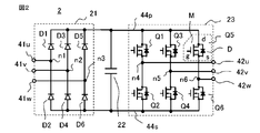
ノイズフィルタ50は、電圧検出器7、分圧回路9、注入波形生成器10、コモンモードトランス11a、11bを備える。電力変換器2は、半導体素子で構成される順変換回路21、直流電力を蓄電する蓄電素子であるコンデンサ22、半導体素子で構成されており、直流電力を交流電力に変換する逆変換回路23を備える。順変換回路21は、例えば整流回路であり、6個のダイオードD1、D2、D3、D4、D5、D6を備えている。逆変換回路23は、6個の半導体素子Q1、Q2、Q3、Q4、Q5、Q6を備えている。一端が交流電源1に接続されている三相電力線4u、4v、4wは、それぞれ他端が電力変換器2の交流入力端子41u、41v、41wに接続されている。一端が誘導電動機3に接続されている三相電力線5u、5v、5wは、それぞれ他端が電力変換器2の交流出力端子42u、42v、42wに接続されている。
The noise filter 50 includes a voltage detector 7, a voltage divider circuit 9, an injection waveform generator 10, and common mode transformers 11a and 11b. The power converter 2 is composed of a forward conversion circuit 21 composed of semiconductor elements, a capacitor 22 which is a storage element for storing DC power, and a reverse conversion circuit 23 which converts DC power into AC power. Be prepared. The forward conversion circuit 21 is, for example, a rectifier circuit, and includes six diodes D1, D2, D3, D4, D5, and D6. The inverse transformation circuit 23 includes six semiconductor elements Q1, Q2, Q3, Q4, Q5, and Q6. The three- phase power lines 4u, 4v, and 4w, one end of which is connected to the AC power supply 1, are connected to the AC input terminals 41u, 41v, and 41w of the power converter 2 at the other ends, respectively. The three- phase power lines 5u, 5v, and 5w whose one end is connected to the induction motor 3 are connected to the AC output terminals 42u, 42v, and 42w of the power converter 2 at the other ends, respectively.
順変換回路21は、高電位側配線44pと低電位側配線44sとの間に、直列に接続されたダイオードD1、D2である第一直列体、直列に接続されたダイオードD3、D4である第二直列体、直列に接続されたダイオードD5、D6である第三直列体が配置されている。ダイオードD1とダイオードD2との接続点n1は、交流入力端子41uに接続されている。ダイオードD3とダイオードD4との接続点n2は交流入力端子41vに接続されており、ダイオードD5とダイオードD6との接続点n3は交流入力端子41wに接続されている。コンデンサ22は、高電位側配線44pと低電位側配線44sとの間に接続されている。逆変換回路23は、高電位側配線44pと低電位側配線44sとの間に、直列に接続された半導体素子Q1、Q2である第四直列体、直列に接続された半導体素子Q3、Q4である第五直列体、直列に接続された半導体素子Q5、Q6である第六直列体が配置されている。半導体素子Q1と半導体素子Q2との接続点n4は、交流出力端子42uに接続されている。半導体素子Q3と半導体素子Q4との接続点n5は交流出力端子42vに接続されており、半導体素子Q5と半導体素子Q6との接続点n6は交流出力端子42wに接続されている。
The forward conversion circuit 21 is a first series body which is a diode D1 and D2 connected in series between the high potential side wiring 44p and the low potential side wiring 44s, and a diode D3 and D4 connected in series. A second series body and a third series body which is a diode D5 and D6 connected in series are arranged. The connection point n1 between the diode D1 and the diode D2 is connected to the AC input terminal 41u. The connection point n2 between the diode D3 and the diode D4 is connected to the AC input terminal 41v, and the connection point n3 between the diode D5 and the diode D6 is connected to the AC input terminal 41w. The capacitor 22 is connected between the high potential side wiring 44p and the low potential side wiring 44s. The inverse conversion circuit 23 is composed of semiconductor elements Q1 and Q2 connected in series between the high potential side wiring 44p and the low potential side wiring 44s, a fourth series body, and semiconductor elements Q3 and Q4 connected in series. A fifth series body and a sixth series body, which are semiconductor elements Q5 and Q6 connected in series, are arranged. The connection point n4 between the semiconductor element Q1 and the semiconductor element Q2 is connected to the AC output terminal 42u. The connection point n5 between the semiconductor element Q3 and the semiconductor element Q4 is connected to the AC output terminal 42v, and the connection point n6 between the semiconductor element Q5 and the semiconductor element Q6 is connected to the AC output terminal 42w.
半導体素子Q1、Q2、Q3、Q4、Q5、Q6は、例えばMOSFET(Metal-Oxide-Semiconductor Field-Effect Transistor)、IGBT(Insulated Gate Bipolar Transistor)等の電力用半導体素子が用いられる。図2では、MOSFETの例を示した。半導体素子Q1、Q2、Q3、Q4、Q5、Q6は、MOSトランジスタM、ダイオードDを備えている。ダイオードDは、MOSトランジスタMと別の素子でもよく、寄生ダイオードでもよい。半導体素子Q1、Q3、Q5のドレインdは高電位側配線44pに接続されており、半導体素子Q2、Q4、Q6のソースsは低電位側配線44sに接続されている。半導体素子Q1のソースsと半導体素子Q2のドレインdは接続されており、半導体素子Q3のソースsと半導体素子Q4のドレインdは接続されており、半導体素子Q5のソースsと半導体素子Q6のドレインdは接続されている。半導体素子Q1、Q2、Q3、Q4、Q5、Q6のゲートgに、図示しない制御回路から制御信号が入力される。逆変換回路23は、制御回路からの制御信号に基づいて半導体素子Q1、Q2、Q3、Q4、Q5、Q6をスイッチングして直流電力を交流電力に変換する。
As the semiconductor elements Q1, Q2, Q3, Q4, Q5, and Q6, for example, semiconductor elements for power such as MOSFET (Metal-Oxide-Semiconductor Field-Effect Transistor) and IGBT (Insulated Gate Bipolar Transistor) are used. FIG. 2 shows an example of MOSFET. The semiconductor elements Q1, Q2, Q3, Q4, Q5, and Q6 include a MOS transistor M and a diode D. The diode D may be an element different from the MOS transistor M, or may be a parasitic diode. The drain d of the semiconductor elements Q1, Q3, and Q5 is connected to the high potential side wiring 44p, and the sources s of the semiconductor elements Q2, Q4, and Q6 are connected to the low potential side wiring 44s. The source s of the semiconductor element Q1 and the drain d of the semiconductor element Q2 are connected, the source s of the semiconductor element Q3 and the drain d of the semiconductor element Q4 are connected, and the source s of the semiconductor element Q5 and the drain of the semiconductor element Q6 are connected. d is connected. A control signal is input from a control circuit (not shown) to the gate g of the semiconductor elements Q1, Q2, Q3, Q4, Q5, and Q6. The inverse conversion circuit 23 switches the semiconductor elements Q1, Q2, Q3, Q4, Q5, and Q6 based on the control signal from the control circuit to convert DC power into AC power.
コモンモード電圧Vciを検出する電圧検出器7は、互いに等しい容量を有する3つのコンデンサ8を備え、各コンデンサ8の一端が三相電力線5の各相に接続されている。各コンデンサ8の他端は接続点n7にて互いに接続されている。分圧回路9は、入力端子94がコンデンサ8の他端が接続された接続点n7に接続され、出力端子95が注入波形生成器10の入力端子51に接続されている。分圧回路9は、接地電位になっている配線24と入力端子94との間の入力電圧であるコモンモード電圧Vciを分圧して、その分圧した分圧電圧Vdを出力電圧として出力する。
The voltage detector 7 that detects the common mode voltage Vci includes three capacitors 8 having equal capacities to each other, and one end of each capacitor 8 is connected to each phase of the three-phase power line 5. The other ends of the capacitors 8 are connected to each other at the connection point n7. In the voltage dividing circuit 9, the input terminal 94 is connected to the connection point n7 to which the other end of the capacitor 8 is connected, and the output terminal 95 is connected to the input terminal 51 of the injection waveform generator 10. The voltage divider circuit 9 divides the common mode voltage Vci, which is the input voltage between the wiring 24 at the ground potential and the input terminal 94, and outputs the divided voltage divider Vd as the output voltage.
分圧回路9は、例えばコンデンサ91と、コンデンサ91に並列に接続された抵抗92及び抵抗93の直列体と、を備えている。コンデンサ91の一端及び抵抗92の一端は入力端子94に接続されており、コンデンサ91の他端及び抵抗93の他端は接地電位になっている配線24に接続されている。抵抗92の他端と抵抗93の一端とが接続された接続点は、出力端子95に接続されている。分圧回路9は、入力端子94に入力されたコモンモード電圧Vciを分圧した分圧電圧Vdを出力端子95から出力する。検出されるコモンモード電圧Vciは抵抗92と抵抗93の抵抗比によって分圧される。三相電力線5の各相である三相電力線5u、5v、5wの電圧は、コンデンサ8とコンデンサ91のインピーダンス比によって分圧された後、抵抗92と抵抗93の抵抗比によって分圧され、分圧電圧Vdとして分圧回路9から出力される。
The voltage dividing circuit 9 includes, for example, a capacitor 91 and a series of resistors 92 and 93 connected in parallel to the capacitor 91. One end of the capacitor 91 and one end of the resistor 92 are connected to the input terminal 94, and the other end of the capacitor 91 and the other end of the resistor 93 are connected to the wiring 24 having a ground potential. The connection point to which the other end of the resistor 92 and one end of the resistor 93 are connected is connected to the output terminal 95. The voltage divider circuit 9 outputs the voltage divider voltage Vd obtained by dividing the common mode voltage Vci input to the input terminal 94 from the output terminal 95. The detected common mode voltage Vci is divided by the resistance ratio of the resistor 92 and the resistor 93. The voltage of the three- phase power lines 5u, 5v, and 5w, which are each phase of the three-phase power line 5, is divided by the impedance ratio of the capacitor 8 and the capacitor 91, and then divided by the resistance ratio of the resistor 92 and the resistor 93. It is output from the voltage divider circuit 9 as the pressure voltage Vd.
分圧電圧Vdは注入波形生成器10の入力端子51に入力される。注入波形生成器10は、入力された分圧電圧Vdに基づいて、帯域制限されかつ電圧値が調整された電圧を出力端子52から出力する。注入波形生成器10の出力端子52から出力される出力はコモンモードトランス11a、11bの一次側すなわち一次巻線に入力される。コモンモードトランス11a、11bは、一次側の一次巻線と二次側の二次巻線を備えており、二次巻線が三相電力線5の各相である三相電力線5u、5v、5wに挿入されている。注入波形生成器10から出力された電圧すなわち出力電圧Vpは各コモンモードトランス11a、11bの一次巻線に印加され、コモンモード電圧Vciと逆極性であり、一次側と二次側の巻数比に応じた電圧である注入電圧Vsが二次巻線に発生する。
The voltage dividing voltage Vd is input to the input terminal 51 of the injection waveform generator 10. The injection waveform generator 10 outputs a voltage whose band is limited and whose voltage value is adjusted based on the input voltage dividing voltage Vd from the output terminal 52. The output output from the output terminal 52 of the injection waveform generator 10 is input to the primary side of the common mode transformers 11a and 11b, that is, the primary winding. The common mode transformers 11a and 11b include a primary winding on the primary side and a secondary winding on the secondary side, and the secondary winding is each phase of the three-phase power line 5, three- phase power lines 5u, 5v, 5w. It is inserted in. The voltage output from the injection waveform generator 10, that is, the output voltage Vp, is applied to the primary windings of the common mode transformers 11a and 11b, has the opposite polarity to the common mode voltage Vci, and has a turns ratio between the primary side and the secondary side. An injection voltage Vs, which is a corresponding voltage, is generated in the secondary winding.
電力変換器2は、半導体素子Q1~Q6がスイッチング動作する毎にステップ状に変化するコモンモード電圧Vciを発生する。このコモンモード電圧Vciは電圧検出器7により検出され、分圧回路9により分圧電圧Vdに分圧される。分圧電圧Vdは注入波形生成器10により帯域制限されかつ電圧値が調整されて出力された出力電圧Vpは、コモンモードトランス11a、11bの一次巻線に入力される。コモンモードトランス11a、11bの二次巻線に発生した電圧すなわち注入電圧Vsは、電力変換器2で発生したコモンモード電圧Vciを低減するように調整されている。したがって、実施の形態1のノイズフィルタ50は、電圧検出器7により検出されたコモンモード電圧Vciに基づいて、コモンモード電圧Vciと逆極性でかつ、調整された電圧である出力電圧Vpをコモンモードトランス11a、11bに入力して三相電力線5の各相に注入電圧Vsを重畳するので、コモンモード電圧Vciを抑制できる。実施の形態1のノイズフィルタ50が、電力変換器2のスイッチング周波数が低い場合でも小型のコモンモードトランス11a、11bを用いてコモンモード電圧Vciを抑制できることを説明する。
The power converter 2 generates a common mode voltage Vci that changes in steps each time the semiconductor elements Q1 to Q6 perform switching operations. This common mode voltage Vci is detected by the voltage detector 7 and is divided into the voltage dividing voltage Vd by the voltage dividing circuit 9. The voltage dividing voltage Vd is band-limited by the injection waveform generator 10, and the output voltage Vp output after adjusting the voltage value is input to the primary windings of the common mode transformers 11a and 11b. The voltage generated in the secondary windings of the common mode transformers 11a and 11b, that is, the injection voltage Vs is adjusted so as to reduce the common mode voltage Vci generated in the power converter 2. Therefore, the noise filter 50 of the first embodiment sets the output voltage Vp, which is a voltage opposite to the common mode voltage Vci and adjusted, based on the common mode voltage Vci detected by the voltage detector 7. Since the injection voltage Vs is superimposed on each phase of the three-phase power line 5 by inputting to the transformers 11a and 11b, the common mode voltage Vci can be suppressed. It will be described that the noise filter 50 of the first embodiment can suppress the common mode voltage Vci by using the small common mode transformers 11a and 11b even when the switching frequency of the power converter 2 is low.
図4~図6に、注入波形生成器10の第一例~第三例を示した。図4に示した第一例の注入波形生成器10は、帯域制限器12、増幅器13、制御電源15a、15bを備えている。制御電源15aは正側電圧を供給し、制御電源15bは負側電圧を供給する。帯域制限器12により、コモンモード電圧Vciのうち低減する周波数帯域のみをコモンモードトランス11a、11bに印加できるため、コモンモードトランス11a、11bの小型化が可能である。帯域制限器12は、対象とする周波数帯域が通過できればよく、バンドパスフィルタ、ローパスフィルタ及び、ハイパスフィルタのいずれかを適用することができる。例えば、スイッチング周波数が2kHzの場合、帯域制限器12の対象とする周波数帯域を2kHzより高い周波数帯域とし、2kHzより低い周波数にカットオフ周波数をもつハイパスフィルタを接続することで、コモンモードトランス11a、11bに印加される電圧の低周波成分を減衰させ、コモンモードトランス11a、11bを小型化できる。また、帯域制限器12の対象とする周波数帯域を10kHzより高い周波数帯域とした場合、2kHz~10kHzの間にカットオフ周波数をもつハイパスフィルタを接続することで、さらにコモンモードトランス11a、11bを小型化することができる。図4に示した増幅器13は反転増幅回路の例である。増幅器13は、オペアンプ19、抵抗16、17、18を備えている。オペアンプ19の正側入力端子に、抵抗17を介して接地電位が入力されている。オペアンプ19の負側入力端子に、帯域制限器12の出力が抵抗16を介して入力され、かつオペアンプ19の出力が抵抗18を介して入力されている。
FIGS. 4 to 6 show first to third examples of the injection waveform generator 10. The injection waveform generator 10 of the first example shown in FIG. 4 includes a band limiter 12, an amplifier 13, and control power supplies 15a and 15b. The control power supply 15a supplies a positive side voltage, and the control power supply 15b supplies a negative side voltage. Since the band limiter 12 can apply only the frequency band to be reduced in the common mode voltage Vci to the common mode transformers 11a and 11b, the common mode transformers 11a and 11b can be miniaturized. The band limiter 12 may apply any of a bandpass filter, a lowpass filter, and a highpass filter as long as it can pass the target frequency band. For example, when the switching frequency is 2 kHz, the target frequency band of the band limiter 12 is set to a frequency band higher than 2 kHz, and a high-pass filter having a cutoff frequency is connected to a frequency lower than 2 kHz. The low frequency component of the voltage applied to 11b can be attenuated, and the common mode transformers 11a and 11b can be miniaturized. Further, when the target frequency band of the band limiter 12 is set to a frequency band higher than 10 kHz, the common mode transformers 11a and 11b can be further reduced in size by connecting a high-pass filter having a cutoff frequency between 2 kHz and 10 kHz. Can be changed. The amplifier 13 shown in FIG. 4 is an example of an inverting amplifier circuit. The amplifier 13 includes an operational amplifier 19, resistors 16, 17, and 18. A ground potential is input to the positive input terminal of the operational amplifier 19 via a resistor 17. The output of the band limiter 12 is input to the negative input terminal of the operational amplifier 19 via the resistor 16, and the output of the operational amplifier 19 is input via the resistor 18.
オペアンプ19のゲインGiは、抵抗16及び抵抗18の抵抗値をそれぞれr1、r2とすると、式(1)で表せる。また、出力電圧Vpは式(2)で表せる。
Gi=r2/r1 ・・・(1)
Vp=-Gi×Vd ・・・(2) The gain Gi of theoperational amplifier 19 can be expressed by the equation (1), where the resistance values of the resistors 16 and 18 are r1 and r2, respectively. Further, the output voltage Vp can be expressed by the equation (2).
Gi = r2 / r1 ... (1)
Vp = -Gi × Vd ・ ・ ・ (2)
Gi=r2/r1 ・・・(1)
Vp=-Gi×Vd ・・・(2) The gain Gi of the
Gi = r2 / r1 ... (1)
Vp = -Gi × Vd ・ ・ ・ (2)
オペアンプ19のゲインGiは、分圧回路9の分圧比Rv、コモンモードトランス11a、11bの巻数比Rr、接続されるコモンモードトランス11a、11bの数である接続トランス数Ntにより設定される。コモンモードトランス11a、11bの二次巻線を介して三相電力線5のu相、v相、w相に重畳される電圧である注入電圧Vsがコモンモード電圧Vciを低減するように、すなわち式(3)が成立するように、ゲインGi、分圧比Rv、巻数比Rr、接続トランス数Ntが設定される。
|Vci-Vst|≦Vtо ・・・(3)
ここで、Vtоは電圧差の許容値である。式(3)は、コモンモード電圧Vciと総注入電圧Vstとの差の絶対値が許容値Vtо以下であることを示している。総注入電圧Vstは、コモンモードトランス11a、11bが発生させる注入電圧Vsを加算した電圧である。 The gain Gi of theoperational amplifier 19 is set by the voltage dividing ratio Rv of the voltage dividing circuit 9, the turns ratio Rr of the common mode transformers 11a and 11b, and the number of connected transformers Nt which is the number of the common mode transformers 11a and 11b to be connected. The injection voltage Vs, which is the voltage superimposed on the u-phase, v-phase, and w-phase of the three-phase power line 5 via the secondary windings of the common mode transformers 11a and 11b, reduces the common mode voltage Vci, that is, the equation. The gain Gi, the voltage division ratio Rv, the turns ratio Rr, and the number of connected transformers Nt are set so that (3) is satisfied.
| Vci-Vst | ≦ Vtо ・ ・ ・ (3)
Here, Vtо is an allowable value of the voltage difference. Equation (3) indicates that the absolute value of the difference between the common mode voltage Vci and the total injection voltage Vst is equal to or less than the allowable value Vtо. The total injection voltage Vst is a voltage obtained by adding the injection voltages Vs generated by the common mode transformers 11a and 11b.
|Vci-Vst|≦Vtо ・・・(3)
ここで、Vtоは電圧差の許容値である。式(3)は、コモンモード電圧Vciと総注入電圧Vstとの差の絶対値が許容値Vtо以下であることを示している。総注入電圧Vstは、コモンモードトランス11a、11bが発生させる注入電圧Vsを加算した電圧である。 The gain Gi of the
| Vci-Vst | ≦ Vtо ・ ・ ・ (3)
Here, Vtо is an allowable value of the voltage difference. Equation (3) indicates that the absolute value of the difference between the common mode voltage Vci and the total injection voltage Vst is equal to or less than the allowable value Vtо. The total injection voltage Vst is a voltage obtained by adding the injection voltages Vs generated by the
注入電圧の電圧値が同一であって接続トランス数Ntが2である場合は、三相電力線5のu相、v相、w相に重畳される電圧の合計である総注入電圧Vstは2×Vsになる。三相電力線5のu相、v相、w相に重畳される電圧の合計である総注入電圧Vstは、接続トランス数Ntを用いると式(4)で表される。図1の場合の接続トランス数Ntは2である。
Vst=Nt×Vs ・・・(4) When the voltage value of the injection voltage is the same and the number of connected transformers Nt is 2, the total injection voltage Vst, which is the total of the voltages superimposed on the u-phase, v-phase, and w-phase of the three-phase power line 5, is 2 ×. It becomes Vs. The total injection voltage Vst, which is the total of the voltages superimposed on the u-phase, v-phase, and w-phase of the three-phase power line 5, is expressed by the equation (4) when the number of connected transformers Nt is used. In the case of FIG. 1, the number of connected transformers Nt is 2.
Vst = Nt × Vs ・ ・ ・ (4)
Vst=Nt×Vs ・・・(4) When the voltage value of the injection voltage is the same and the number of connected transformers Nt is 2, the total injection voltage Vst, which is the total of the voltages superimposed on the u-phase, v-phase, and w-phase of the three-
Vst = Nt × Vs ・ ・ ・ (4)
分圧回路9の分圧比Rvは、式(5)で表せる。コモンモードトランス11a、11bの巻数比Rrは、一次巻線及び二次巻線の巻数をそれぞれN1、N2とすると、式(6)で表せる。
Rv=Vci/Vd ・・・(5)
Rr=N2/N1 ・・・(6) The voltage dividing ratio Rv of thevoltage dividing circuit 9 can be expressed by the equation (5). The turns ratio Rr of the common mode transformers 11a and 11b can be expressed by the equation (6), where N1 and N2 are the turns of the primary winding and the secondary winding, respectively.
Rv = Vci / Vd ・ ・ ・ (5)
Rr = N2 / N1 ... (6)
Rv=Vci/Vd ・・・(5)
Rr=N2/N1 ・・・(6) The voltage dividing ratio Rv of the
Rv = Vci / Vd ・ ・ ・ (5)
Rr = N2 / N1 ... (6)
あるコモンモード電圧Vciの値に対して、接続トランス数Ntが多い程、1つのコモンモードトランスに入力される電圧すなわち注入波形生成器10の出力電圧Vpとコモンモードトランスの二次巻線に出力される電圧である注入電圧Vsとを小さくすることができる。複数のコモンモードトランス11a、11bを備えることで、実施の形態1のノイズフィルタ50は、小型のコモンモードトランス11a、11bで総注入電圧Vstを三相電力線5のu相、v相、w相に重畳することができる。したがって、実施の形態1のノイズフィルタ50は、スイッチング周波数が低い場合でも小型のコモンモードトランスを用いてコモンモード電圧を抑制できる。注入電圧Vsを小さくすることでコモンモードトランスが小型にできることは、後述する。
As the number of connected transformers Nt increases with respect to a certain common mode voltage Vci value, the voltage input to one common mode transformer, that is, the output voltage Vp of the injection waveform generator 10 and the output to the secondary winding of the common mode transformer. The injection voltage Vs, which is the voltage to be applied, can be reduced. By providing a plurality of common mode transformers 11a and 11b, the noise filter 50 of the first embodiment has a small common mode transformers 11a and 11b with a total injection voltage Vst of the u-phase, v-phase, and w-phase of the three-phase power line 5. Can be superimposed on. Therefore, the noise filter 50 of the first embodiment can suppress the common mode voltage by using a small common mode transformer even when the switching frequency is low. It will be described later that the common mode transformer can be made smaller by reducing the injection voltage Vs.
第二例の注入波形生成器10を説明する。第二例の注入波形生成器10は、第一例の注入波形生成器10とは、増幅器13の出力端子と出力端子52との間に電流バッファ14が追加されている点で異なる。なお、増幅器13の出力端子は、オペアンプ19の出力を伝送する配線と抵抗18との接続点である。第二例の注入波形生成器10は、第一例の注入波形生成器10よりも電流供給量を示す電流容量を増やすことが可能である。電流バッファ14は、例えば直列接続された2つのトランジスタBT1、BT2を備えている。トランジスタBT1のコレクタcが制御電源15aに接続されており、トランジスタBT1のエミッタeがトランジスタBT2のエミッタeに接続されており、トランジスタBT2のコレクタcが制御電源15bに接続されている。トランジスタBT1、BT2のベースbは増幅器13の出力が入力され、トランジスタBT1、BT2のエミッタeは出力端子52に接続されている。
The injection waveform generator 10 of the second example will be described. The injection waveform generator 10 of the second example is different from the injection waveform generator 10 of the first example in that a current buffer 14 is added between the output terminal and the output terminal 52 of the amplifier 13. The output terminal of the amplifier 13 is a connection point between the wiring that transmits the output of the operational amplifier 19 and the resistor 18. The injection waveform generator 10 of the second example can increase the current capacity indicating the amount of current supply as compared with the injection waveform generator 10 of the first example. The current buffer 14 includes, for example, two transistors BT1 and BT2 connected in series. The collector c of the transistor BT1 is connected to the control power supply 15a, the emitter e of the transistor BT1 is connected to the emitter e of the transistor BT2, and the collector c of the transistor BT2 is connected to the control power supply 15b. The output of the amplifier 13 is input to the base b of the transistors BT1 and BT2, and the emitter e of the transistors BT1 and BT2 is connected to the output terminal 52.
第一例の注入波形生成器10、第二例の注入波形生成器10では、増幅器13が反転増幅回路の例を示したが、増幅器13が非反転増幅回路であってもよい。図6に示した第三例の注入波形生成器10は非反転増幅回路の例である。オペアンプ19の正側入力端子に、抵抗17を介して帯域制限器12の出力が入力されている。オペアンプ19の負側入力端子に、接地電位が抵抗16を介して入力され、かつオペアンプ19の出力が抵抗18を介して入力されている。
In the injection waveform generator 10 of the first example and the injection waveform generator 10 of the second example, the amplifier 13 shows an example of an inverting amplifier circuit, but the amplifier 13 may be a non-inverting amplifier circuit. The injection waveform generator 10 of the third example shown in FIG. 6 is an example of a non-inverting amplifier circuit. The output of the band limiter 12 is input to the positive input terminal of the operational amplifier 19 via the resistor 17. The ground potential is input to the negative input terminal of the operational amplifier 19 via the resistor 16, and the output of the operational amplifier 19 is input via the resistor 18.
非反転増幅回路のオペアンプ19のゲインGiは、抵抗16及び抵抗18の抵抗値をそれぞれr1、r2とすると、式(7)で表せる。また、出力電圧Vpは式(8)で表せる。
Gi=1+r2/r1 ・・・(7)
Vp=Gi×Vd ・・・(8) The gain Gi of theoperational amplifier 19 of the non-inverting amplifier circuit can be expressed by the equation (7), where the resistance values of the resistors 16 and 18 are r1 and r2, respectively. Further, the output voltage Vp can be expressed by the equation (8).
Gi = 1 + r2 / r1 ... (7)
Vp = Gi × Vd ・ ・ ・ (8)
Gi=1+r2/r1 ・・・(7)
Vp=Gi×Vd ・・・(8) The gain Gi of the
Gi = 1 + r2 / r1 ... (7)
Vp = Gi × Vd ・ ・ ・ (8)
増幅器13が非反転増幅回路の場合、図7に示すように、コモンモードトランス11a、11bの一次巻線への接続を逆に変更し、二次巻線に出力される電圧である注入電圧Vsがコモンモード電圧Vciを低減するように設定する。次に、実施の形態1のノイズフィルタ50を、比較例のノイズフィルタ100と比較しながら説明する。
When the amplifier 13 is a non-inverting amplifier circuit, as shown in FIG. 7, the connection to the primary winding of the common mode transformers 11a and 11b is changed in reverse, and the injection voltage Vs which is the voltage output to the secondary winding is changed. Is set to reduce the common mode voltage Vci. Next, the noise filter 50 of the first embodiment will be described while comparing it with the noise filter 100 of the comparative example.
図9に示した比較例のノイズフィルタ100は1つのコモンモードトランス101を備えており、比較例の電動機駆動システム110はノイズフィルタ100を備えている。比較例のノイズフィルタ100は、注入波形生成器102からコモンモードトランス101の一次巻線に出力電圧Vpeが出力され、三相電力線5のu相、v相、w相に注入電圧Vseを重畳させる。比較例のノイズフィルタ100は、実施の形態1のノイズフィルタ50とは、1つのコモンモードトランス101を備え、注入波形生成器10が注入波形生成器102に変更されている点で異なる。注入波形生成器102は注入波形生成器10と同様の構成であるが、出力電圧Vpeの値によってはゲインGi等が異なる。比較例のノイズフィルタ100は、接続トランス数Ntが1である。コモンモードトランスの数が異なっても同等のコモンモード電圧の低下を実現するには、同じ値の総注入電圧Vstが必要である。このため、式(4)から分かるように、比較例のノイズフィルタ100は、接続トランス数Ntが2である実施の形態1のノイズフィルタ50が三相電力線5の各相に重畳させる注入電圧Vsの2倍になる注入電圧Vseを三相電力線5の各相に重畳しないと同等のコモンモード電圧の低下を実現することはできない。しがたって、比較例のノイズフィルタ100は、実施の形態1のノイズフィルタ50と同等のコモンモード電圧の低下を実現するには、式(9)が成立する必要がある。
Vse=2×Vs ・・・(9) Thenoise filter 100 of the comparative example shown in FIG. 9 includes one common mode transformer 101, and the motor drive system 110 of the comparative example includes a noise filter 100. In the noise filter 100 of the comparative example, the output voltage Vpe is output from the injection waveform generator 102 to the primary winding of the common mode transformer 101, and the injection voltage Vse is superimposed on the u-phase, v-phase, and w-phase of the three-phase power line 5. .. The noise filter 100 of the comparative example is different from the noise filter 50 of the first embodiment in that it includes one common mode transformer 101 and the injection waveform generator 10 is changed to the injection waveform generator 102. The injection waveform generator 102 has the same configuration as the injection waveform generator 10, but the gain Gi and the like differ depending on the value of the output voltage Vpe. The noise filter 100 of the comparative example has a connected transformer number Nt of 1. In order to achieve the same reduction in common mode voltage even if the number of common mode transformers is different, the total injection voltage Vst of the same value is required. Therefore, as can be seen from the equation (4), in the noise filter 100 of the comparative example, the injection voltage Vs superposed on each phase of the three-phase power line 5 by the noise filter 50 of the first embodiment in which the number of connected transformers Nt is 2. Unless the injection voltage Vse, which is twice as high as that of the above, is superimposed on each phase of the three-phase power line 5, the same reduction in common mode voltage cannot be realized. Therefore, in the noise filter 100 of the comparative example, the equation (9) needs to be satisfied in order to realize the same reduction of the common mode voltage as the noise filter 50 of the first embodiment.
Vse = 2 × Vs ・ ・ ・ (9)
Vse=2×Vs ・・・(9) The
Vse = 2 × Vs ・ ・ ・ (9)
式(9)を実現させるには、例えば2つの方法が考えられる。第一の方法は、出力電圧Vpeを出力電圧Vpと同じにして、コモンモードトランス101の巻数比Rrを2倍にすることである。第二の方法は、コモンモードトランス101の巻数比Rrをコモンモードトランス11a、11bの巻数比Rrと同じにして、出力電圧Vpeを出力電圧Vpの2倍にすることである。
For example, two methods can be considered to realize the equation (9). The first method is to make the output voltage Vpe the same as the output voltage Vp and double the turns ratio Rr of the common mode transformer 101. The second method is to make the turns ratio Rr of the common mode transformer 101 the same as the turn ratio Rr of the common mode transformers 11a and 11b, and to make the output voltage Vpe twice the output voltage Vp.
コモンモードトランス11a、11bは、1つの一次巻線及び3つの二次巻線を備えている。コモンモードトランス11a、11bのコアは例えば図10に示すトロイダル型のコア28である。実施の形態1のノイズフィルタ50は2つのコモンモードトランス11a、11bを備えているので、図12に示すように2つのコア28を備えている。比較例のコモンモードトランス101も、コモンモードトランス11a、11bと同様である。比較例のノイズフィルタ100は1つのコモンモードトランス101を備えているので、図13に示すように1つのコア29を備えている。コアのサイズについては後述する。
The common mode transformers 11a and 11b include one primary winding and three secondary windings. The cores of the common mode transformers 11a and 11b are, for example, the toroidal type core 28 shown in FIG. Since the noise filter 50 of the first embodiment includes two common mode transformers 11a and 11b, it includes two cores 28 as shown in FIG. The common mode transformer 101 of the comparative example is also the same as the common mode transformers 11a and 11b. Since the noise filter 100 of the comparative example includes one common mode transformer 101, it includes one core 29 as shown in FIG. The size of the core will be described later.
第一の方法において、コモンモードトランス101の巻数比Rrを大きくするには、一次巻線の巻数を減らす方法と二次巻線の巻数を増やす方法がある。一次巻線の巻数を減らす場合、コモンモードトランス101の励磁電流が増加し磁束も増加する。コモンモードトランス101に使用するコアの磁気飽和を避けるには、コアの断面積を増加させる必要がある。対して、二次巻線の巻数を増やす場合、二次巻線には三相電力線5と同等の線径を有する巻線が3相分巻かれているため、コアに必要な内径が大きくなるので、結果として、コアが大型化する。制御電源15a、15bの電圧値以上の電圧を注入電圧Vseとしてコモンモードトランス101の二次巻線に発生させる場合、コアの大型化は避けられない。
In the first method, in order to increase the turns ratio Rr of the common mode transformer 101, there are a method of reducing the number of turns of the primary winding and a method of increasing the number of turns of the secondary winding. When the number of turns of the primary winding is reduced, the exciting current of the common mode transformer 101 increases and the magnetic flux also increases. In order to avoid magnetic saturation of the core used in the common mode transformer 101, it is necessary to increase the cross-sectional area of the core. On the other hand, when increasing the number of turns of the secondary winding, since the secondary winding has three windings having a wire diameter equivalent to that of the three-phase power line 5, the inner diameter required for the core becomes large. Therefore, as a result, the core becomes large. When a voltage equal to or higher than the voltage values of the control power supplies 15a and 15b is generated in the secondary winding of the common mode transformer 101 as the injection voltage Vse, it is inevitable to increase the size of the core.
一方、第二の方法において、コモンモードトランス101に高電圧を印加するには、高電圧を出力する制御電源、高耐圧素子が必要となる。また、コモンモードトランス101における電圧時間積が大きくなるため、コアの磁気飽和を避けるには、コアの断面積の増加、一次巻線の巻数増加が必要となる。巻数比Rrを一定に保つために二次巻線の巻数も増加することになり、結果として、コモンモードトランス101に高電圧を印加する場合もコアの大型化につながる。
On the other hand, in the second method, in order to apply a high voltage to the common mode transformer 101, a control power supply and a high withstand voltage element that output a high voltage are required. Further, since the voltage-time product in the common mode transformer 101 becomes large, it is necessary to increase the cross-sectional area of the core and the number of turns of the primary winding in order to avoid magnetic saturation of the core. In order to keep the turns ratio Rr constant, the number of turns of the secondary winding also increases, and as a result, even when a high voltage is applied to the common mode transformer 101, the size of the core is increased.
以上のことから、実施の形態1のノイズフィルタ50では、複数のコモンモードトランス11a、11bを備えることで、1つのコモンモードトランスで発生させる注入電圧Vsを小さくできる。このため、実施の形態1のノイズフィルタ50は、比較例のノイズフィルタ100と異なり、コモンモードトランス11a、11bはコアの断面積を大きくする必要がなく、巻数増加のためにコア内径を大きくする必要がなく、コアを小型化することが可能である。また、実施の形態1のノイズフィルタ50は、コモンモードトランス11a、11bに印加する電圧すなわち出力電圧Vpは低電圧で良く、電圧時間積を小さくできるため、コアの小型化が図れる。加えて、実施の形態1のノイズフィルタ50は、注入波形生成器10に印加する制御電源15a、15bの電圧は低電圧で良く、注入波形生成器10を低耐圧の素子で構成することが可能である。
From the above, the noise filter 50 of the first embodiment is provided with a plurality of common mode transformers 11a and 11b, so that the injection voltage Vs generated by one common mode transformer can be reduced. Therefore, unlike the noise filter 100 of the comparative example, the noise filter 50 of the first embodiment does not need to increase the cross-sectional area of the core of the common mode transformers 11a and 11b, and increases the inner diameter of the core in order to increase the number of turns. There is no need, and the core can be miniaturized. Further, in the noise filter 50 of the first embodiment, the voltage applied to the common mode transformers 11a and 11b, that is, the output voltage Vp may be a low voltage, and the voltage time product can be reduced, so that the core can be miniaturized. In addition, in the noise filter 50 of the first embodiment, the voltages of the control power supplies 15a and 15b applied to the injection waveform generator 10 may be low, and the injection waveform generator 10 can be configured by a low withstand voltage element. Is.
特許文献1のコモンモード抑制回路は、巻数比Rrが1のコモンモードトランスが1つである。前述したように、スイッチング周波数が低い場合、コアに発生する磁束の時間積が大きくなるので、同じ電圧を二次巻線に発生させるためにコモンモードトランスに使用されるコアが大きくなる。1つコモンモードトランスでは、このサイズ増大が顕著になる。実施の形態1のノイズフィルタ50は2つのコモンモードトランス11a、11bを備えるので、特許文献1のコモンモード抑制回路が三相電力線5に重畳する総注入電圧Vstが同じ場合には、各コモンモードトランス11a、11bが重畳する注入電圧VsをVst/2にすることができる。注入電圧VsがVst/2になるので、電圧時間積を小さくでき、さらにコアに発生させる磁束も小さくでき、コアの断面積を小さくすることができる。したがって、実施の形態1のノイズフィルタ50は、特許文献1のコモンモード抑制回路よりも小型のコアを有するコモンモードトランスを用いることができる。
The common mode suppression circuit of Patent Document 1 has one common mode transformer having a turns ratio Rr of 1. As described above, when the switching frequency is low, the time product of the magnetic flux generated in the core becomes large, so that the core used for the common mode transformer to generate the same voltage in the secondary winding becomes large. With one common mode transformer, this size increase becomes remarkable. Since the noise filter 50 of the first embodiment includes two common mode transformers 11a and 11b, when the total injection voltage Vst superimposed on the three-phase power line 5 by the common mode suppression circuit of Patent Document 1 is the same, each common mode The injection voltage Vs on which the transformers 11a and 11b are superimposed can be set to Vst / 2. Since the injection voltage Vs becomes Vst / 2, the voltage time product can be made small, the magnetic flux generated in the core can be made small, and the cross-sectional area of the core can be made small. Therefore, as the noise filter 50 of the first embodiment, a common mode transformer having a core smaller than that of the common mode suppression circuit of Patent Document 1 can be used.
実施の形態1のノイズフィルタ50におけるコアのサイズについて、図10~図13を用いて説明する。実施の形態1のノイズフィルタ50におけるコアは、前述したように例えば図10に示すトロイダル型のコア28である。実施の形態1のノイズフィルタ50は2つのコモンモードトランス11a、11bを備えているので、図12に示すように2つのコア28を備えている。比較例のノイズフィルタ100は1つのコモンモードトランス101を備えているので、図13に示すように1つのコア29を備えている。コア28の内径はlであり、外径はLであり、幅(厚み)はhである。コア28の断面積がSである。図11において、左側がコア28の内側であり、右側がコア28の外側である。まず、図1のように2つのコモンモードトランス11a、11bに同一電圧値の出力電圧Vpを印加する場合を考える。コア28に発生する磁束密度Bは式(10)で表せる。
B=(Vp×t)/(N1×S) ・・・(10)
tは出力電圧Vpを印加する時間である。 The size of the core in thenoise filter 50 of the first embodiment will be described with reference to FIGS. 10 to 13. The core in the noise filter 50 of the first embodiment is, for example, the toroidal type core 28 shown in FIG. 10 as described above. Since the noise filter 50 of the first embodiment includes two common mode transformers 11a and 11b, it includes two cores 28 as shown in FIG. Since the noise filter 100 of the comparative example includes one common mode transformer 101, it includes one core 29 as shown in FIG. The inner diameter of the core 28 is l, the outer diameter is L, and the width (thickness) is h. The cross-sectional area of the core 28 is S. In FIG. 11, the left side is the inside of the core 28, and the right side is the outside of the core 28. First, consider a case where an output voltage Vp having the same voltage value is applied to the two common mode transformers 11a and 11b as shown in FIG. The magnetic flux density B generated in the core 28 can be expressed by the equation (10).
B = (Vp × t) / (N1 × S) ・ ・ ・ (10)
t is the time for applying the output voltage Vp.
B=(Vp×t)/(N1×S) ・・・(10)
tは出力電圧Vpを印加する時間である。 The size of the core in the
B = (Vp × t) / (N1 × S) ・ ・ ・ (10)
t is the time for applying the output voltage Vp.
式(10)から電圧時間積(Vp×t)を小さくすることで、磁束密度Bと一次側の巻数N1を一定にしながら断面積Sを小さくできる。比較例のコモンモードトランス101のコア29に発生する磁束密度と実施の形態11の2つのコモンモードトランス11a、11bのコア28に発生する合計の磁束密度が同じになる場合を考えると、コア28の断面積Sとコア29の断面積Seとの関係は式(11)のようになる。
Se=2×S ・・・(11) By reducing the voltage time product (Vp × t) from the equation (10), the cross-sectional area S can be reduced while keeping the magnetic flux density B and the number of turns N1 on the primary side constant. Considering the case where the magnetic flux density generated in thecore 29 of the common mode transformer 101 of the comparative example and the total magnetic flux density generated in the core 28 of the two common mode transformers 11a and 11b of the eleventh embodiment are the same, the core 28 is considered. The relationship between the cross-sectional area S of the core 29 and the cross-sectional area Se of the core 29 is as shown in the equation (11).
Se = 2 × S ・ ・ ・ (11)
Se=2×S ・・・(11) By reducing the voltage time product (Vp × t) from the equation (10), the cross-sectional area S can be reduced while keeping the magnetic flux density B and the number of turns N1 on the primary side constant. Considering the case where the magnetic flux density generated in the
Se = 2 × S ・ ・ ・ (11)
コア29の断面積Se及び体積v1は式(12)、(13)で表せる。コア29の断面積Seは、図10のコア28をコア29とした場合におけるA-Aで示した破線に沿った断面の面積になる。コア29の幅は、コア28の幅と同じhである。
Se=h×(Le-l)/2 ・・・(12)
v1=π×h×(Le2-l2)/4 ・・・(13) The cross-sectional area Se and the volume v1 of the core 29 can be expressed by the equations (12) and (13). The cross-sectional area Se of thecore 29 is the area of the cross section along the broken line shown by AA when the core 28 in FIG. 10 is used as the core 29. The width of the core 29 is the same h as the width of the core 28.
Se = h × (Le-l) / 2 ... (12)
v1 = π × h × (Le 2- l 2 ) / 4 ・ ・ ・ (13)
Se=h×(Le-l)/2 ・・・(12)
v1=π×h×(Le2-l2)/4 ・・・(13) The cross-sectional area Se and the volume v1 of the core 29 can be expressed by the equations (12) and (13). The cross-sectional area Se of the
Se = h × (Le-l) / 2 ... (12)
v1 = π × h × (Le 2- l 2 ) / 4 ・ ・ ・ (13)
コア28の断面積S及び体積v2は式(14)、(15)で表せる。
S=h×(L-l)/2 ・・・(14)
v2=π×h×(L2-l2)/4 ・・・(15) The cross-sectional area S and volume v2 of the core 28 can be expressed by equations (14) and (15).
S = h × (L−l) / 2 ・ ・ ・ (14)
v2 = π × h × (L 2- l 2 ) / 4 ・ ・ ・ (15)
S=h×(L-l)/2 ・・・(14)
v2=π×h×(L2-l2)/4 ・・・(15) The cross-sectional area S and volume v2 of the core 28 can be expressed by equations (14) and (15).
S = h × (L−l) / 2 ・ ・ ・ (14)
v2 = π × h × (L 2- l 2 ) / 4 ・ ・ ・ (15)
式(11)に式(12)(14)を代入して変形すると、式(16)のようになる。
L=(Le+l)/2 ・・・(16) Substituting equations (12) and (14) into equation (11) and transforming it gives equation (16).
L = (Le + l) / 2 ... (16)
L=(Le+l)/2 ・・・(16) Substituting equations (12) and (14) into equation (11) and transforming it gives equation (16).
L = (Le + l) / 2 ... (16)
式(15)の体積v2は、式(16)を用いて変形すると式(17)のようになる。
v2=π×h×(Le2+2Le×l-3l2)/16 ・・・(17) The volume v2 of the formula (15) is transformed into the formula (17) by using the formula (16).
v2 = π × h × (Le 2 + 2 Le × l-3l 2 ) / 16 ・ ・ ・ (17)
v2=π×h×(Le2+2Le×l-3l2)/16 ・・・(17) The volume v2 of the formula (15) is transformed into the formula (17) by using the formula (16).
v2 = π × h × (Le 2 + 2 Le × l-3l 2 ) / 16 ・ ・ ・ (17)
式(13)と式(17)から、コア29の体積v1と2つのコア28の合計体積2×v2は式(18)の関係が成り立つ。
v1>2×v2 ・・・(18) From the equations (13) and (17), the relationship of the equation (18) is established for the volume v1 of thecore 29 and the total volume 2 × v2 of the two cores 28.
v1> 2 × v2 ・ ・ ・ (18)
v1>2×v2 ・・・(18) From the equations (13) and (17), the relationship of the equation (18) is established for the volume v1 of the
v1> 2 × v2 ・ ・ ・ (18)
このことから、1つのコモンモードトランス101と同一電圧値の出力電圧Vpを2つのコモンモードトランス11a、11bで分割して、同一電圧値の注入電圧Vsを三相電力線5に重畳する場合は、次のようになる。実施の形態1のノイズフィルタ50におけるコモンモードトランス11a、11bは、磁束密度Bと内径lが一定の条件のもと、1つのコア28における外径Lを外径Leよりも小さくすることで、1つのコア28における断面積Sをコア29の断面積Seの1/2に維持しながら、コア28の合計体積すなわち合計サイズを小さくすることができる。ここで内径lが一定であることは、巻数N1が一定であり必要内径が一定であることによる。
From this, when the output voltage Vp having the same voltage value as one common mode transformer 101 is divided by the two common mode transformers 11a and 11b and the injection voltage Vs having the same voltage value is superimposed on the three-phase power line 5. It looks like this: The common mode transformers 11a and 11b in the noise filter 50 of the first embodiment have the outer diameter L of one core 28 smaller than the outer diameter Le under the condition that the magnetic flux density B and the inner diameter l are constant. The total volume or total size of the core 28 can be reduced while maintaining the cross-sectional area S of one core 28 at half the cross-sectional area Se of the core 29. Here, the constant inner diameter l is due to the fact that the number of turns N1 is constant and the required inner diameter is constant.
また、図8のように、コモンモードトランス11a、11bが異なる電圧値の注入電圧Vsa、Vsbを三相電力線5に重畳する場合は、特許文献1のコモンモードトランスと異なり、許容値に合わせて総電圧を減らすという操作が可能であるため、コア28の断面積Sを小さくでき、2つのコア28の合計体積(合計サイズ)を小さくすることができる。
Further, as shown in FIG. 8, when the common mode transformers 11a and 11b superimpose the injection voltages Vsa and Vsb having different voltage values on the three-phase power line 5, unlike the common mode transformer of Patent Document 1, the allowable values are adjusted. Since the operation of reducing the total voltage is possible, the cross-sectional area S of the core 28 can be reduced, and the total volume (total size) of the two cores 28 can be reduced.
実施の形態1のノイズフィルタ50は、2つのコモンモードトランスの合計サイズを特許文献1のコモンモードトランスよりも小さくすることができる。実施の形態1のノイズフィルタ50は、小型のコモンモードトランスを2つ用いることで、特許文献1のコモンモード抑制回路よりもコモンモードトランスの配置自由度が高くなる。このため、実施の形態1のノイズフィルタ50は、特許文献1のコモンモード抑制回路よりも効率的な部品配置が可能となり、小型のノイズフィルタを実現できる。さらに、実施の形態1のノイズフィルタ50は、注入波形生成器10がコア増大に大きな影響を及ぼす周波数を排除する帯域制限を分圧電圧Vdに行うことで、特許文献1のコモンモードトランスよりもさらに小さくすることができる。つまり、複数のコモンモードトランス11a、11bによる注入電圧Vsが充分に低電圧化されている場合は、コア増大に大きな影響を及ぼす周波数を排除する帯域制限を行わなくても、特許文献1のコモンモードトランスよりもコモンモードトランス11a、11bを小さくすることができる。
The noise filter 50 of the first embodiment can make the total size of the two common mode transformers smaller than that of the common mode transformer of Patent Document 1. The noise filter 50 of the first embodiment uses two small common mode transformers, so that the degree of freedom in arranging the common mode transformers is higher than that of the common mode suppression circuit of Patent Document 1. Therefore, the noise filter 50 of the first embodiment enables more efficient component arrangement than the common mode suppression circuit of Patent Document 1, and can realize a small noise filter. Further, the noise filter 50 of the first embodiment is more than the common mode transformer of Patent Document 1 by applying a band limitation to the voltage dividing voltage Vd to eliminate the frequency at which the injection waveform generator 10 has a great influence on the core increase. It can be made even smaller. That is, when the injection voltage Vs by the plurality of common mode transformers 11a and 11b is sufficiently lowered, the common of Patent Document 1 is performed even if the band limitation for excluding the frequency having a great influence on the core increase is not performed. The common mode transformers 11a and 11b can be made smaller than the mode transformer.
特許文献1のコモンモード抑制回路は、制御電源の電力がインバータの入力側直流電源の電力であるため、高耐圧のトランジスタが必要である。これに対して実施の形態1のノイズフィルタ50は、注入電圧Vsが特許文献1のコモンモード抑制回路の注入電圧の1/2になり、注入波形生成器10が出力する出力電圧Vpを特許文献1のコモンモード抑制回路よりも低電圧にできる。このため、注入波形生成器10を低耐圧の素子で構成することができる。
The common mode suppression circuit of Patent Document 1 requires a high withstand voltage transistor because the power of the control power supply is the power of the DC power supply on the input side of the inverter. On the other hand, in the noise filter 50 of the first embodiment, the injection voltage Vs becomes 1/2 of the injection voltage of the common mode suppression circuit of Patent Document 1, and the output voltage Vp output by the injection waveform generator 10 is patented. The voltage can be made lower than that of the common mode suppression circuit of 1. Therefore, the injection waveform generator 10 can be configured with a low withstand voltage element.
コモンモードトランス11a、11bはコア材、コア28の外径L、内径l、断面積S及び巻数N1、N2が同じ場合を示したが、コア材、コア28の外径L、内径l、断面積S及び巻数N1、N2のいずれかが異なっていてもよい。この場合、図8に示すように、コモンモードトランス11a、11bに入力される注入波形生成器10の出力電圧Vpが同じでも、コモンモードトランス11aが発生させる注入電圧Vsaとコモンモードトランス11bが発生させる注入電圧Vsbとが異なることもある。この場合は、総注入電圧Vstは式(4)の代わりに式(19)を用いる。
Vst=Vsa+Vsb ・・・(19) The common mode transformers 11a and 11b show the case where the core material and the core 28 have the same outer diameter L, inner diameter l, cross-sectional area S and turns N1 and N2, but the core material and the core 28 have the same outer diameter L, inner diameter l and disconnection. Either the area S and the number of turns N1 or N2 may be different. In this case, as shown in FIG. 8, even if the output voltage Vp of the injection waveform generator 10 input to the common mode transformers 11a and 11b is the same, the injection voltage Vsa generated by the common mode transformer 11a and the common mode transformer 11b are generated. The injection voltage Vsb to be made may be different. In this case, the total injection voltage Vst uses the equation (19) instead of the equation (4).
Vst = Vsa + Vsb ... (19)
Vst=Vsa+Vsb ・・・(19) The
Vst = Vsa + Vsb ... (19)
注入電圧Vsaと注入電圧Vsbが異なる場合でも、比較例及び特許文献1のコモンモード抑制回路と比較して説明した注入電圧Vsを総注入電圧Vstの1/2と考えればよい。したがって、実施の形態1のノイズフィルタ50は、比較例のノイズフィルタ100及び特許文献1のコモンモード抑制回路のコモンモードトランスよりも、コモンモードトランス11a、11bを小型にすることができる。
Even when the injection voltage Vsa and the injection voltage Vsb are different, the injection voltage Vs described in comparison with the comparative example and the common mode suppression circuit of Patent Document 1 may be considered as 1/2 of the total injection voltage Vst. Therefore, the noise filter 50 of the first embodiment can make the common mode transformers 11a and 11b smaller than the noise filter 100 of the comparative example and the common mode transformer of the common mode suppression circuit of Patent Document 1.
なお、図1に示した電圧検出器7は三相電力線5に接続されている例を示したが、図14に示すように電圧検出器7は三相電力線4への接続も可能である。電力変換器2は三相電力線4にもコモンモード電圧Vciを発生させている。この場合でも、三相電力線4から検出されるコモンモード電圧Vciは三相電力線5から検出されるコモンモード電圧Vciと同等なので、式(3)を満たせばよい。また、コモンモードトランス11a、11bは三相電力線5に挿入されている例を示したが、図15に示すようにコモンモードトランス11a、11bは三相電力線4に挿入することも可能である。三相電力線4でのコモンモード電圧Vciを低減することで、三相電力線5でのコモンモード電圧Vciを低減することができる。図15では電圧検出器7が三相電力線4に接続されている例を示したが、電圧検出器7が三相電力線5に接続されていても構わない。更に、図16に示すように、コモンモードトランス11a、11bと電圧検出器7との位置を交換しても構わない。図1に示した第一例のノイズフィルタ50はフィードフォワード構成であるが、図16に示した第六例のノイズフィルタ50はフィードバック構成である。
Although the voltage detector 7 shown in FIG. 1 is connected to the three-phase power line 5, the voltage detector 7 can also be connected to the three-phase power line 4 as shown in FIG. The power converter 2 also generates a common mode voltage Vci in the three-phase power line 4. Even in this case, since the common mode voltage Vci detected from the three-phase power line 4 is equivalent to the common mode voltage Vci detected from the three-phase power line 5, the equation (3) may be satisfied. Further, although the example in which the common mode transformers 11a and 11b are inserted into the three-phase power line 5 is shown, the common mode transformers 11a and 11b can also be inserted into the three-phase power line 4 as shown in FIG. By reducing the common mode voltage Vci in the three-phase power line 4, the common mode voltage Vci in the three-phase power line 5 can be reduced. Although FIG. 15 shows an example in which the voltage detector 7 is connected to the three-phase power line 4, the voltage detector 7 may be connected to the three-phase power line 5. Further, as shown in FIG. 16, the positions of the common mode transformers 11a and 11b and the voltage detector 7 may be exchanged. The noise filter 50 of the first example shown in FIG. 1 has a feedforward configuration, while the noise filter 50 of the sixth example shown in FIG. 16 has a feedback configuration.
分圧回路9の例としてコンデンサ91と抵抗92、93を備える例を示したが、分圧回路9はこれに限定されない。分圧回路9は、2つのコンデンサが直列接続されたコンデンサ91のみの構成、抵抗92、93のみの構成、さらにコンデンサと抵抗の数を増やした構成も可能である。
As an example of the voltage dividing circuit 9, an example including a capacitor 91 and resistors 92 and 93 is shown, but the voltage dividing circuit 9 is not limited to this. The voltage dividing circuit 9 can be configured with only a capacitor 91 in which two capacitors are connected in series, a configuration with only resistors 92 and 93, and a configuration in which the number of capacitors and resistors is increased.
以上のように、実施の形態1のノイズフィルタ50は、半導体素子Q1~Q6のスイッチング動作により電力変換を行う電力変換器2が発生させるコモンモード電圧Vciを低減するノイズフィルタである。ノイズフィルタ50は、電力変換器2が発生させるコモンモード電圧Vciを検出する電圧検出器7と、電圧検出器7により検出されたコモンモード電圧Vciを分圧した分圧電圧Vdを出力する分圧回路9と、コモンモード電圧Vciと逆極性の注入電圧Vs(Vsa、Vsb)を電力変換器2の出力又は入力に重畳させる複数のコモンモードトランス11a、11bと、分圧電圧Vdに基づいて複数のコモンモードトランス11a、11bの一次側に出力する出力電圧Vpを生成する注入波形生成器10と、を備えている。注入波形生成器10は、複数のコモンモードトランス11a、11bにより重畳させる注入電圧Vs(Vsa、Vsb)を加算した総注入電圧Vstとコモンモード電圧Vciとの差が許容値Vtо以下になる出力電圧Vpを生成する。実施の形態1のノイズフィルタ50は、この構成により、複数のコモンモードトランス11a、11bを備え、注入波形生成器10が複数のコモンモードトランス11a、11bにより重畳させる注入電圧Vs(Vsa、Vsb)を加算した総注入電圧Vstとコモンモード電圧Vciとの差が許容値Vtо以下になる出力電圧Vpを生成するので、スイッチング周波数が低い場合でも小型のコモンモードトランス11a、11bを用いてコモンモード電圧Vciを抑制できる。
As described above, the noise filter 50 of the first embodiment is a noise filter that reduces the common mode voltage Vci generated by the power converter 2 that performs power conversion by the switching operation of the semiconductor elements Q1 to Q6. The noise filter 50 outputs a voltage divider 7 that detects the common mode voltage Vci generated by the power converter 2 and a voltage divider Vd that is obtained by dividing the common mode voltage Vci detected by the voltage detector 7. The circuit 9, a plurality of common mode transformers 11a and 11b for superimposing an injection voltage Vs (Vsa, Vsb) having a polarity opposite to the common mode voltage Vci on the output or input of the power converter 2, and a plurality of common mode transformers 11a and 11b based on the voltage dividing voltage Vd. The injection waveform generator 10 for generating an output voltage Vp to be output to the primary side of the common mode transformers 11a and 11b of the above is provided. The injection waveform generator 10 has an output voltage in which the difference between the total injection voltage Vst obtained by adding the injection voltages Vs (Vsa, Vsb) superimposed by the plurality of common mode transformers 11a and 11b and the common mode voltage Vci is equal to or less than the allowable value Vtо. Generate Vp. With this configuration, the noise filter 50 of the first embodiment includes a plurality of common mode transformers 11a and 11b, and the injection waveform generator 10 superimposes the injection voltage Vs (Vsa, Vsb) on the plurality of common mode transformers 11a and 11b. Since the output voltage Vp at which the difference between the total injection voltage Vst and the common mode voltage Vci is equal to or less than the allowable value Vtо is generated, even if the switching frequency is low, the common mode voltage is used by using the small common mode transformers 11a and 11b. Vci can be suppressed.
実施の形態2.
図17は、実施の形態2に係る第一のノイズフィルタ及び電動機駆動システムの構成を示す図である。図18は図17の第一の注入波形生成器の第一例を示す図であり、図19は図17の第二の注入波形生成器の第一例を示す図である。図20は図17の第一の注入波形生成器の第二例を示す図であり、図21は図17の第二の注入波形生成器の第二例を示す図である。図22は図17の第一の注入波形生成器の第三例を示す図であり、図23は図17の第二の注入波形生成器の第三例を示す図である。図24は図17の第一の注入波形生成器の第四例を示す図であり、図25は図17の第二の注入波形生成器の第四例を示す図である。図26は図17の第一の注入波形生成器の第五例を示す図であり、図27は図17の第二の注入波形生成器の第五例を示す図である。図28は図17の第一の注入波形生成器の第六例を示す図であり、図29は図17の第二の注入波形生成器の第六例を示す図である。図30は実施の形態2に係る第二のノイズフィルタ及び電動機駆動システムの構成を示す図であり、図31は実施の形態2に係る第三のノイズフィルタ及び電動機駆動システムの構成を示す図である。Embodiment 2.
FIG. 17 is a diagram showing the configuration of the first noise filter and the motor drive system according to the second embodiment. FIG. 18 is a diagram showing a first example of the first injection waveform generator of FIG. 17, and FIG. 19 is a diagram showing a first example of the second injection waveform generator of FIG. 20 is a diagram showing a second example of the first injection waveform generator of FIG. 17, and FIG. 21 is a diagram showing a second example of the second injection waveform generator of FIG. 22 is a diagram showing a third example of the first injection waveform generator of FIG. 17, and FIG. 23 is a diagram showing a third example of the second injection waveform generator of FIG. FIG. 24 is a diagram showing a fourth example of the first injection waveform generator of FIG. 17, and FIG. 25 is a diagram showing a fourth example of the second injection waveform generator of FIG. FIG. 26 is a diagram showing a fifth example of the first injection waveform generator of FIG. 17, and FIG. 27 is a diagram showing a fifth example of the second injection waveform generator of FIG. FIG. 28 is a diagram showing a sixth example of the first injection waveform generator of FIG. 17, and FIG. 29 is a diagram showing a sixth example of the second injection waveform generator of FIG. FIG. 30 is a diagram showing the configuration of the second noise filter and the motor drive system according to the second embodiment, and FIG. 31 is a diagram showing the configuration of the third noise filter and the motor drive system according to the second embodiment. be.
図17は、実施の形態2に係る第一のノイズフィルタ及び電動機駆動システムの構成を示す図である。図18は図17の第一の注入波形生成器の第一例を示す図であり、図19は図17の第二の注入波形生成器の第一例を示す図である。図20は図17の第一の注入波形生成器の第二例を示す図であり、図21は図17の第二の注入波形生成器の第二例を示す図である。図22は図17の第一の注入波形生成器の第三例を示す図であり、図23は図17の第二の注入波形生成器の第三例を示す図である。図24は図17の第一の注入波形生成器の第四例を示す図であり、図25は図17の第二の注入波形生成器の第四例を示す図である。図26は図17の第一の注入波形生成器の第五例を示す図であり、図27は図17の第二の注入波形生成器の第五例を示す図である。図28は図17の第一の注入波形生成器の第六例を示す図であり、図29は図17の第二の注入波形生成器の第六例を示す図である。図30は実施の形態2に係る第二のノイズフィルタ及び電動機駆動システムの構成を示す図であり、図31は実施の形態2に係る第三のノイズフィルタ及び電動機駆動システムの構成を示す図である。
FIG. 17 is a diagram showing the configuration of the first noise filter and the motor drive system according to the second embodiment. FIG. 18 is a diagram showing a first example of the first injection waveform generator of FIG. 17, and FIG. 19 is a diagram showing a first example of the second injection waveform generator of FIG. 20 is a diagram showing a second example of the first injection waveform generator of FIG. 17, and FIG. 21 is a diagram showing a second example of the second injection waveform generator of FIG. 22 is a diagram showing a third example of the first injection waveform generator of FIG. 17, and FIG. 23 is a diagram showing a third example of the second injection waveform generator of FIG. FIG. 24 is a diagram showing a fourth example of the first injection waveform generator of FIG. 17, and FIG. 25 is a diagram showing a fourth example of the second injection waveform generator of FIG. FIG. 26 is a diagram showing a fifth example of the first injection waveform generator of FIG. 17, and FIG. 27 is a diagram showing a fifth example of the second injection waveform generator of FIG. FIG. 28 is a diagram showing a sixth example of the first injection waveform generator of FIG. 17, and FIG. 29 is a diagram showing a sixth example of the second injection waveform generator of FIG. FIG. 30 is a diagram showing the configuration of the second noise filter and the motor drive system according to the second embodiment, and FIG. 31 is a diagram showing the configuration of the third noise filter and the motor drive system according to the second embodiment. be.
図17に示した実施の形態2のノイズフィルタ50は、2つの注入波形生成器10a、10bにより3つのコモンモードトランス11a、11b、11cに出力電圧Vpa、Vpb、Vpcが出力され、3つのコモンモードトランス11a、11b、11cが三相電力線5の各相に注入電圧Vsa、Vsb、Vscを発生させる点で、実施の形態1のノイズフィルタ50と異なる。図18に示した第一の注入波形生成器10aの第一例は、図4に示した注入波形生成器10とは、帯域制限器12が低周波数帯域を通過させ高周波数帯域を減少させる帯域制限器32に変更され、2つの出力端子52a、52bを有する点で異なる。図19に示した第二の注入波形生成器10bの第一例は、図4に示した注入波形生成器10とは、帯域制限器12が高周波数帯域を通過させ低周波数帯域を減少させる帯域制限器33に変更されている点で異なる。注入波形生成器10aは、出力端子52aから出力電圧Vpaを出力し、出力端子52bから出力電圧Vpbを出力する。注入波形生成器10bは、出力端子52から出力電圧Vpcを出力する。なお、図18、図19において、接地電位になっている配線24は省略した。図20~図29においても、接地電位になっている配線24は省略した。なお、実施の形態2のノイズフィルタ50は、2つの波形生成器(注入波形生成器10a、10b)を備えた注入波形生成器を備えているということもできる。
In the noise filter 50 of the second embodiment shown in FIG. 17, the output voltages Vpa, Vpb, and Vpc are output to the three common mode transformers 11a, 11b, and 11c by the two injection waveform generators 10a and 10b, and the three commons. It differs from the noise filter 50 of the first embodiment in that the mode transformers 11a, 11b, and 11c generate injection voltages Vsa, Vsb, and Vsc in each phase of the three-phase power line 5. In the first example of the first injection waveform generator 10a shown in FIG. 18, the injection waveform generator 10 shown in FIG. 4 is a band in which the band limiter 12 passes through a low frequency band and reduces a high frequency band. It is changed to the limiter 32 and differs in that it has two output terminals 52a and 52b. In the first example of the second injection waveform generator 10b shown in FIG. 19, the injection waveform generator 10 shown in FIG. 4 is a band in which the band limiter 12 passes through a high frequency band and reduces a low frequency band. It differs in that it has been changed to the limiter 33. The injection waveform generator 10a outputs an output voltage Vpa from the output terminal 52a and outputs an output voltage Vpb from the output terminal 52b. The injection waveform generator 10b outputs an output voltage Vpc from the output terminal 52. In addition, in FIGS. 18 and 19, the wiring 24 which is the ground potential is omitted. Also in FIGS. 20 to 29, the wiring 24 having the ground potential is omitted. It can also be said that the noise filter 50 of the second embodiment includes an injection waveform generator including two waveform generators ( injection waveform generators 10a and 10b).
実施の形態1のノイズフィルタ50と異なる部分を主に説明する。注入波形生成器10aは低周波数帯域のみ増幅し、高周波数帯域は減少させるよう設定される。一方、注入波形生成器10bは高周波数帯域のみ増幅し、低周波数帯域は減少させるよう設定される。すなわち、注入波形生成器10aは低周波数帯域の出力電圧Vpa、Vpbをコモンモードトランス11a、11bに出力し、注入波形生成器10bは高周波数帯域の出力電圧Vpcをコモンモードトランス11cに出力する。出力電圧Vpa、Vpbは出力電圧Vpcとは周波数帯域が異なっている。これにより、注入波形生成器10aに接続されるコモンモードトランス11a、11bには低周波数帯域の電圧が印加され、注入波形生成器10bに接続されるコモンモードトランス11cは高周波数帯域の電圧が印加される。また、出力電圧Vpa、Vpbは出力電圧Vpcとは周波数帯域に応じて電圧値が異なっていてもよい。
The part different from the noise filter 50 of the first embodiment will be mainly described. The injection waveform generator 10a is set to amplify only the low frequency band and decrease the high frequency band. On the other hand, the injection waveform generator 10b is set to amplify only the high frequency band and decrease the low frequency band. That is, the injection waveform generator 10a outputs the output voltages Vpa and Vpb in the low frequency band to the common mode transformers 11a and 11b, and the injection waveform generator 10b outputs the output voltage Vpc in the high frequency band to the common mode transformer 11c. The frequency bands of the output voltages Vpa and Vpb are different from those of the output voltage Vpc. As a result, a low frequency band voltage is applied to the common mode transformers 11a and 11b connected to the injection waveform generator 10a, and a high frequency band voltage is applied to the common mode transformer 11c connected to the injection waveform generator 10b. Will be done. Further, the output voltages Vpa and Vpb may have different voltage values from the output voltage Vpc depending on the frequency band.
一般に、トランスに印加する電圧が高周波数帯域になるほどコア材の性質によりコア内に発生する磁束は少ない。つまり磁束が少なくなることに伴ってトランスにおける電圧時間積が小さいため、トランスが必要とするコアの断面積は小さくなる。したがって、高周波数帯域が印加されるコモンモードトランス11cはコモンモードトランス11a、11bと比較し、小型化することが可能である。
Generally, the higher the frequency band of the voltage applied to the transformer, the smaller the magnetic flux generated in the core due to the properties of the core material. That is, as the magnetic flux decreases, the voltage-time product in the transformer becomes smaller, so that the cross-sectional area of the core required by the transformer becomes smaller. Therefore, the common mode transformer 11c to which the high frequency band is applied can be downsized as compared with the common mode transformers 11a and 11b.
また、コア28の断面積Sを小さくする代わりにコモンモードトランス11cの巻数N1、N2を減らすことでもコモンモードトランス11cを小型化することができる。巻数N1、N2を減らす場合、コア28に必要となる内径lが小さくなる。コア28の断面積Sを一定とした場合、内径lを小さくすると外径Lも小さくすることができるため、結果として、コモンモードトランス11cの小型化が可能となる。これらは同時に行うことも可能であり、トランスにおける電圧時間積が小さい場合は、コア28の断面積Sを小さくしつつ、巻数N1、N2を減らしコア28の外径L、内径lを小さくすることも可能である。
Further, the common mode transformer 11c can be miniaturized by reducing the turns N1 and N2 of the common mode transformer 11c instead of reducing the cross-sectional area S of the core 28. When the number of turns N1 and N2 is reduced, the inner diameter l required for the core 28 becomes smaller. When the cross-sectional area S of the core 28 is constant, the outer diameter L can be reduced by reducing the inner diameter l, and as a result, the common mode transformer 11c can be miniaturized. These can be performed at the same time, and when the voltage time product in the transformer is small, the cross-sectional area S of the core 28 is reduced, the turns N1 and N2 are reduced, and the outer diameter L and inner diameter l of the core 28 are reduced. Is also possible.
一般に、トランスはインダクタンスと寄生容量による自己共振の影響を受け、高周波数帯域でインピーダンスが低下し、励磁電流が増加する。この自己共振周波数はコア材により異なるため、高周波数帯域の電圧が印加されるコモンモードトランス11cに自己共振周波数が高く、高周波数帯域においても高いインピーダンスをもつコア材を使用することで、励磁電流を低減することができる。これにより、注入波形生成器10bに電力を供給する制御電源15a、15bの電力供給量を示す電源容量を低減することが可能である。
Generally, transformers are affected by self-resonance due to inductance and parasitic capacitance, impedance decreases in the high frequency band, and exciting current increases. Since this self-resonant frequency differs depending on the core material, the exciting current is excited by using a core material having a high self-resonance frequency and high impedance even in the high frequency band for the common mode transformer 11c to which a voltage in the high frequency band is applied. Can be reduced. This makes it possible to reduce the power supply capacity indicating the power supply amount of the control power supplies 15a and 15b that supply power to the injection waveform generator 10b.
このように、この実施の形態2では2つの注入波形生成器10a、10bを異なる構成とし、3つのコモンモードトランス11a、11b、11cを異なる構成とし、印加する電圧を低周波数帯域と高周波数帯域とに分離することで、コモンモードトランスのコアの小型化及び制御電源15a、15bの電源容量の低減が可能になる。制御電源15a、15bの電源容量を低減した場合は、例えば増幅器13のゲインGiを増加することで、出力電圧Vpa、Vpb、Vpcを制御電源15a、15bの電源容量を低減しない場合と同じにすることができる。
As described above, in the second embodiment, the two injection waveform generators 10a and 10b have different configurations, and the three common mode transformers 11a, 11b, and 11c have different configurations, and the applied voltages are in the low frequency band and the high frequency band. By separating into and, it is possible to reduce the size of the core of the common mode transformer and the power supply capacities of the control power supplies 15a and 15b. When the power supply capacities of the control power supplies 15a and 15b are reduced, for example, by increasing the gain Gi of the amplifier 13, the output voltages Vpa, Vpb and Vpc are made the same as when the power supply capacities of the control power supplies 15a and 15b are not reduced. be able to.
図20に示した第一の注入波形生成器10aの第二例は、図5に示した注入波形生成器10とは、帯域制限器12が低周波数帯域を通過させ高周波数帯域を減少させる帯域制限器32に変更され、2つの出力端子52a、52bを有する点で異なる。図21に示した第二の注入波形生成器10bの第二例は、図5に示した注入波形生成器10とは、帯域制限器12が高周波数帯域を通過させ低周波数帯域を減少させる帯域制限器33に変更されている点で異なる。注入波形生成器10aは、出力端子52aから出力電圧Vpaを出力し、出力端子52bから出力電圧Vpbを出力する。注入波形生成器10bは、出力端子52から出力電圧Vpcを出力する。また、第一の注入波形生成器10aの第二例は、第一の注入波形生成器10aの第一例とは、増幅器13の出力端子と出力端子52a、52bとの間に電流バッファ14が追加されている点で異なる。第二の注入波形生成器10bの第二例は、第二の注入波形生成器10bの第一例とは、増幅器13の出力端子と出力端子52との間に電流バッファ14が追加されている点で異なる。第一の注入波形生成器10aの第二例及び第二の注入波形生成器10bの第二例は、電流バッファ14により第一例の注入波形生成器10a、10bに比べて電流供給量を示す電流容量を増やすことが可能である。
In the second example of the first injection waveform generator 10a shown in FIG. 20, the injection waveform generator 10 shown in FIG. 5 is a band in which the band limiter 12 passes through the low frequency band and reduces the high frequency band. It is changed to the limiter 32 and differs in that it has two output terminals 52a and 52b. In the second example of the second injection waveform generator 10b shown in FIG. 21, the injection waveform generator 10 shown in FIG. 5 is a band in which the band limiter 12 passes through the high frequency band and reduces the low frequency band. It differs in that it has been changed to the limiter 33. The injection waveform generator 10a outputs an output voltage Vpa from the output terminal 52a and outputs an output voltage Vpb from the output terminal 52b. The injection waveform generator 10b outputs an output voltage Vpc from the output terminal 52. Further, in the second example of the first injection waveform generator 10a, in the first example of the first injection waveform generator 10a, a current buffer 14 is provided between the output terminal of the amplifier 13 and the output terminals 52a and 52b. It differs in that it has been added. In the second example of the second injection waveform generator 10b, a current buffer 14 is added between the output terminal and the output terminal 52 of the amplifier 13 as in the first example of the second injection waveform generator 10b. It differs in that. The second example of the first injection waveform generator 10a and the second example of the second injection waveform generator 10b show the current supply amount by the current buffer 14 as compared with the injection waveform generators 10a and 10b of the first example. It is possible to increase the current capacity.
図22に示した第一の注入波形生成器10aの第三例は、図18に示した第一の注入波形生成器10aの第一例とは、入力端子51側に帯域制限器32がなく、増幅器13の出力端子と出力端子52a、52bとの間にそれぞれ帯域制限器32a、32bが配置されている点で異なる。帯域制限器32aの周波数帯域と帯域制限器32bの周波数帯域は同じでもよく、異なっていてもよい。帯域制限器32aの周波数帯域と帯域制限器32bの周波数帯域が異なる場合は、周波数帯域の異なる出力電圧Vpa、Vpbを出力することができる。なお、出力電圧Vpa、Vpbの周波数帯域は、出力電圧Vpcよりも低い周波数帯域である。図23に示した第二の注入波形生成器10bの第三例は、図19に示した第二の注入波形生成器10bの第一例とは、入力端子51側に帯域制限器33がなく、増幅器13の出力端子と出力端子52との間に帯域制限器33が配置されている点で異なる。
The third example of the first injection waveform generator 10a shown in FIG. 22 has no band limiter 32 on the input terminal 51 side as the first example of the first injection waveform generator 10a shown in FIG. The difference is that the band limiters 32a and 32b are arranged between the output terminals of the amplifier 13 and the output terminals 52a and 52b, respectively. The frequency band of the band limiter 32a and the frequency band of the band limiter 32b may be the same or different. When the frequency band of the band limiter 32a and the frequency band of the band limiter 32b are different, the output voltages Vpa and Vpb having different frequency bands can be output. The frequency band of the output voltages Vpa and Vpb is a frequency band lower than the output voltage Vpc. The third example of the second injection waveform generator 10b shown in FIG. 23 is different from the first example of the second injection waveform generator 10b shown in FIG. 19 without the band limiter 33 on the input terminal 51 side. The difference is that the band limiter 33 is arranged between the output terminal and the output terminal 52 of the amplifier 13.
図24に示した第一の注入波形生成器10aの第四例は、第一の注入波形生成器10aの第三例とは、増幅器13の出力端子と帯域制限器32a、32bの入力側との間に電流バッファ14が追加されている点で異なる。図25に示した第二の注入波形生成器10bの第四例は、第二の注入波形生成器10bの第三例とは、増幅器13の出力端子と帯域制限器33の入力側との間に電流バッファ14が追加されている点で異なる。第一の注入波形生成器10aの第四例及び第二の注入波形生成器10bの第四例は、電流バッファ14により第三例の注入波形生成器10a、10bに比べて電流供給量を示す電流容量を増やすことが可能である。
In the fourth example of the first injection waveform generator 10a shown in FIG. 24, the third example of the first injection waveform generator 10a is the output terminal of the amplifier 13 and the input side of the band limiters 32a and 32b. The difference is that the current buffer 14 is added between the two. The fourth example of the second injection waveform generator 10b shown in FIG. 25 is that the third example of the second injection waveform generator 10b is between the output terminal of the amplifier 13 and the input side of the band limiter 33. The difference is that the current buffer 14 is added to. The fourth example of the first injection waveform generator 10a and the fourth example of the second injection waveform generator 10b show the current supply amount by the current buffer 14 as compared with the injection waveform generators 10a and 10b of the third example. It is possible to increase the current capacity.
図24に示した第一の注入波形生成器10aの第四例は、増幅器13の出力端子と帯域制限器32a、32bの入力側との間に電流バッファ14が配置されている例であるが、電流バッファ14は帯域制限器32a、32bの出力側と出力端子52a、52bとの間に配置されてもよい。図26に示した第一の注入波形生成器10aの第五例は、第一の注入波形生成器10aの第三例とは、帯域制限器32aの出力側と出力端子52aとの間に電流バッファ14aが追加され、帯域制限器32bの出力側と出力端子52bとの間に電流バッファ14bが追加されている点で異なる。第一の注入波形生成器10aの第五例は、電流バッファ14a、14bにより第三例の注入波形生成器10aに比べて電流供給量を示す電流容量を増やすことが可能である。
The fourth example of the first injection waveform generator 10a shown in FIG. 24 is an example in which the current buffer 14 is arranged between the output terminal of the amplifier 13 and the input side of the band limiters 32a and 32b. , The current buffer 14 may be arranged between the output side of the band limiters 32a and 32b and the output terminals 52a and 52b. The fifth example of the first injection waveform generator 10a shown in FIG. 26 is different from the third example of the first injection waveform generator 10a in that the current is between the output side of the band limiter 32a and the output terminal 52a. The difference is that a buffer 14a is added and a current buffer 14b is added between the output side of the band limiter 32b and the output terminal 52b. In the fifth example of the first injection waveform generator 10a, the current buffers 14a and 14b can increase the current capacity indicating the current supply amount as compared with the injection waveform generator 10a of the third example.
同様に、図25に示した第二の注入波形生成器10bの第四例は、増幅器13の出力端子と帯域制限器33の入力側との間に電流バッファ14が配置されている例であるが、電流バッファ14は帯域制限器33の出力側と出力端子52との間に配置されてもよい。図27に示した第二の注入波形生成器10bの第五例は、第二の注入波形生成器10bの第三例とは、帯域制限器33の出力側と出力端子52との間に電流バッファ14が追加されている点で異なる。第二の注入波形生成器10bの第五例は、電流バッファ14により第三例の注入波形生成器10bに比べて電流供給量を示す電流容量を増やすことが可能である。
Similarly, the fourth example of the second injection waveform generator 10b shown in FIG. 25 is an example in which the current buffer 14 is arranged between the output terminal of the amplifier 13 and the input side of the band limiter 33. However, the current buffer 14 may be arranged between the output side of the band limiter 33 and the output terminal 52. The fifth example of the second injection waveform generator 10b shown in FIG. 27 is different from the third example of the second injection waveform generator 10b in that the current is between the output side of the band limiter 33 and the output terminal 52. The difference is that the buffer 14 is added. In the fifth example of the second injection waveform generator 10b, the current buffer 14 can increase the current capacity indicating the current supply amount as compared with the injection waveform generator 10b of the third example.
図28に示した第一の注入波形生成器10aの第六例は、第一の注入波形生成器10aの第三例とは、入力端子51と増幅器13の入力側との間に帯域制限器32cが配置されている点で異なる。図29に示した第二の注入波形生成器10bの第六例は、第二の注入波形生成器10bの第三例とは、入力端子51と増幅器13の入力側との間に帯域制限器34が配置されている点で異なる。帯域制限器32cの周波数帯域は、帯域制限器32a、32bと同様に、第二の注入波形生成器10bにおける帯域制限器33、34よりも低い周波数帯域である。帯域制限器34の周波数帯域は、帯域制限器33と同様に、第一の注入波形生成器10aにおける帯域制限器32a、32b、32cよりも高い周波数帯域である。
The sixth example of the first injection waveform generator 10a shown in FIG. 28 is a band limiter between the input terminal 51 and the input side of the amplifier 13 with the third example of the first injection waveform generator 10a. It differs in that 32c is arranged. In the sixth example of the second injection waveform generator 10b shown in FIG. 29, the third example of the second injection waveform generator 10b is a band limiter between the input terminal 51 and the input side of the amplifier 13. It differs in that 34 is arranged. The frequency band of the band limiter 32c is a lower frequency band than the band limiters 33 and 34 in the second injection waveform generator 10b, similarly to the band limiters 32a and 32b. The frequency band of the band limiter 34 is a higher frequency band than the band limiters 32a, 32b, 32c in the first injection waveform generator 10a, similarly to the band limiter 33.
第一の注入波形生成器10aの第六例は、入力側にも帯域制限器32cを備えているので、出力側の帯域制限器32a、32bを小型にできる。このため第一の注入波形生成器10aの第六例は、小型の帯域制限器32a、32b、32cにより、2つの帯域制限器32a、32bを備える第一の注入波形生成器10aの第三例のよりも帯域制限器の合計消費電力を低減することができる。第二の注入波形生成器10bの第六例は、入力側にも帯域制限器34を備えているので、出力側の帯域制限器33を小型にできる。このため第一の注入波形生成器10bの第六例は、小型の帯域制限器33、34により、1つの帯域制限器33を備える第二の注入波形生成器10bの第三例のよりも帯域制限器の合計消費電力を低減することができる。
Since the sixth example of the first injection waveform generator 10a is also provided with the band limiter 32c on the input side, the band limiters 32a and 32b on the output side can be miniaturized. Therefore, the sixth example of the first injection waveform generator 10a is the third example of the first injection waveform generator 10a provided with two band limiters 32a, 32b by the small band limiters 32a, 32b, 32c. The total power consumption of the band limiter can be reduced more than that of. In the sixth example of the second injection waveform generator 10b, since the band limiter 34 is also provided on the input side, the band limiter 33 on the output side can be made smaller. Therefore, the sixth example of the first injection waveform generator 10b has a smaller band than the third example of the second injection waveform generator 10b including one band limiter 33 due to the small band limiters 33 and 34. The total power consumption of the limiter can be reduced.
図17では注入波形生成器が2つあり、コモンモードトランスが3つである場合を示したが、それぞれの数を限定するものではない。例えば図30のように、2つのコモンモードトランス11a、11cに対して2つの注入波形生成器10a、10bから出力電圧Vpa、Vpcを出力するようにしてもよい。図30に示した実施の形態2の第二のノイズフィルタ50は、図1に示した実施の形態1のノイズフィルタ50とは、2つの注入波形生成器10a、10bにより2つのコモンモードトランス11a、11cに出力電圧Vpa、Vpcが出力されている点で異なる。
FIG. 17 shows a case where there are two injection waveform generators and three common mode transformers, but the number of each is not limited. For example, as shown in FIG. 30, the output voltages Vpa and Vpc may be output from the two injection waveform generators 10a and 10b for the two common mode transformers 11a and 11c. The second noise filter 50 of the second embodiment shown in FIG. 30 is different from the noise filter 50 of the first embodiment shown in FIG. 1 by two injection waveform generators 10a and 10b and two common mode transformers 11a. , 11c is different in that the output voltages Vpa and Vpc are output.
また、例えば図31のように、2つのコモンモードトランス11a、11cに対して1つの注入波形生成器10aから出力電圧Vpa、Vpcを出力するようにしてもよい。この場合の注入波形生成器10aは、出力端子52a、52bの側に帯域制限器32a、32bを備えている、図22、図24、図26、図28に示した注入波形生成器10aを適用できる。
Further, for example, as shown in FIG. 31, the output voltages Vpa and Vpc may be output from one injection waveform generator 10a for the two common mode transformers 11a and 11c. In this case, the injection waveform generator 10a to which the band limiters 32a and 32b are provided on the output terminals 52a and 52b is applied to the injection waveform generator 10a shown in FIGS. 22, 24, 26 and 28. can.
また、注入波形生成器10a、10bは周波数帯域が異なるすなわち周波数特性が異なる場合を示したが、同じゲイン及び周波数特性でも構成可能である。この場合の実施の形態2のノイズフィルタ50は、実質的に実施の形態1のノイズフィルタ50と同じ作用を生じるので、実施の形態1のノイズフィルタ50と同様の効果を奏する。なお、注入波形生成器10a、10bはそれぞれ異なるゲインの増幅器13を備え、異なる電圧値の出力電圧Vpa、Vpcを出力するようにしてもよい。
Further, although the injection waveform generators 10a and 10b have shown the case where the frequency bands are different, that is, the frequency characteristics are different, the same gain and frequency characteristics can be configured. In this case, the noise filter 50 of the second embodiment has substantially the same operation as the noise filter 50 of the first embodiment, and thus has the same effect as the noise filter 50 of the first embodiment. The injection waveform generators 10a and 10b may be provided with amplifiers 13 having different gains, and may output output voltages Vpa and Vpc of different voltage values.
コモンモードトランス11a、11b、11cはコア材、コア28の外径L、内径l、断面積S及び巻数N1、N2が異なる場合を示したが、同じコア材、コア28の外径L、内径l、断面積S及び巻数N1、N2でも構成可能である。
The common mode transformers 11a, 11b, and 11c show the case where the core material, the outer diameter L of the core 28, the inner diameter l, the cross-sectional area S, and the number of turns N1 and N2 are different. It can also be configured with l, the cross-sectional area S, and the number of turns N1 and N2.
なお、実施の形態1及び実施の形態2のノイズフィルタ50は、三相交流電力から直流電力を介して三相交流電力に変換する電力変換器2を搭載した電動機駆動システム60に適用した例を示したが、この例に限定されない。実施の形態1及び実施の形態2のノイズフィルタ50は、半導体素子のスイッチング動作によりコモンモード電圧を発生する電力変換器が搭載されたシステムにも適用できる。例えば、電力変換器2が絶縁型DC-DCコンバータであってもよい。この場合、交流電源1は直流電源になり、誘導電動機3は直流電動機になる。
An example in which the noise filter 50 of the first embodiment and the second embodiment is applied to an electric motor drive system 60 equipped with a power converter 2 that converts three-phase AC power to three-phase AC power via DC power. Although shown, it is not limited to this example. The noise filter 50 of the first embodiment and the second embodiment can also be applied to a system equipped with a power converter that generates a common mode voltage by a switching operation of a semiconductor element. For example, the power converter 2 may be an isolated DC-DC converter. In this case, the AC power supply 1 becomes a DC power supply, and the induction motor 3 becomes a DC motor.
以上のように、実施の形態2のノイズフィルタ50は、低周波数帯域の出力電圧Vpaが入力されるコモンモードトランス11aと高周波数帯域の出力電圧Vpcが入力されるコモンモードトランス11cとを備えるので、高周波数帯域用のコモンモードトランス11cを低周波帯域用のコモンモードトランス11aよりも小型にできる。このため、実施の形態2のノイズフィルタ50は、特許文献1のコモンモードトランスよりも小型にでき、スイッチング周波数が低い場合でも小型のコモンモードトランスを用いてコモンモード電圧を抑制できる。また、実施の形態2のノイズフィルタ50は、高周波数帯域のコモンモードトランス11cよりも大きくなる低周波数帯域のコモンモードトランスを複数設けることで、実施の形態1で説明したように、1個当たりの注入電圧Vsa、Vsbが小さくなるので、さらに各コモンモードトランス11a、11bが小型にでき、特許文献1のコモンモードトランスよりも小型にできる。
As described above, the noise filter 50 of the second embodiment includes the common mode transformer 11a to which the output voltage Vpa in the low frequency band is input and the common mode transformer 11c to which the output voltage Vpc in the high frequency band is input. The common mode transformer 11c for the high frequency band can be made smaller than the common mode transformer 11a for the low frequency band. Therefore, the noise filter 50 of the second embodiment can be made smaller than the common mode transformer of Patent Document 1, and the common mode voltage can be suppressed by using the small common mode transformer even when the switching frequency is low. Further, the noise filter 50 of the second embodiment is provided with a plurality of common mode transformers of a low frequency band which are larger than the common mode transformer 11c of the high frequency band, so that each noise filter 50 is provided as described in the first embodiment. Since the injection voltages Vsa and Vsb of the above are smaller, the common mode transformers 11a and 11b can be made smaller, and can be made smaller than the common mode transformer of Patent Document 1.
なお、本願は、様々な例示的な実施の形態及び実施例が記載されているが、1つ、または複数の実施の形態に記載された様々な特徴、態様、及び機能は特定の実施の形態の適用に限られるのではなく、単独で、または様々な組み合わせで実施の形態に適用可能である。従って、例示されていない無数の変形例が、本願明細書に開示される技術の範囲内において想定される。例えば、少なくとも1つの構成要素を変形する場合、追加する場合または省略する場合、さらには、少なくとも1つの構成要素を抽出し、他の実施の形態の構成要素と組み合わせる場合が含まれるものとする。
Although various exemplary embodiments and examples are described in the present application, the various features, embodiments, and functions described in one or more embodiments are specific embodiments. It is not limited to the application of, but can be applied to the embodiment alone or in various combinations. Therefore, innumerable variations not exemplified are envisioned within the scope of the techniques disclosed herein. For example, it is assumed that at least one component is modified, added or omitted, and further, at least one component is extracted and combined with the components of other embodiments.
2…電力変換器、7…電圧検出器、9…分圧回路、10…注入波形生成器、10a、10b…注入波形生成器(波形生成器)、11a、11b、11c…コモンモードトランス、12…帯域制限器、13…増幅器、28…コア、32、32a、32b、32c…帯域制限器、33…帯域制限器、34…帯域制限器、50…ノイズフィルタ、52、52a、52b…出力端子、Gi…ゲイン、l…内径、L…外径、Nt…接続トランス数、Q1、Q2、Q3、Q4、Q5、Q6…半導体素子、Rr…巻数比、S…断面積、Vci…コモンモード電圧、Vd…分圧電圧、Vp、Vpa、Vpb、Vpc…出力電圧、Vs、Vsa、Vsb、Vsc…注入電圧、Vst…総注入電圧
2 ... Power converter, 7 ... Voltage detector, 9 ... Voltage divider circuit, 10 ... Injection waveform generator, 10a, 10b ... Injection waveform generator (waveform generator), 11a, 11b, 11c ... Common mode transformer, 12 ... band limiter, 13 ... amplifier, 28 ... core, 32, 32a, 32b, 32c ... band limiter, 33 ... band limiter, 34 ... band limiter, 50 ... noise filter, 52, 52a, 52b ... output terminal , Gi ... Gain, l ... Inner diameter, L ... Outer diameter, Nt ... Number of connected transformers, Q1, Q2, Q3, Q4, Q5, Q6 ... Semiconductor element, Rr ... Turn ratio, S ... Cross section, Vci ... Common mode voltage , Vd ... voltage dividing voltage, Vp, Vpa, Vpb, Vpc ... output voltage, Vs, Vsa, Vsb, Vsc ... injection voltage, Vst ... total injection voltage
Claims (15)
- 半導体素子のスイッチング動作により電力変換を行う電力変換器が発生させるコモンモード電圧を低減するノイズフィルタであって、
前記電力変換器が発生させる前記コモンモード電圧を検出する電圧検出器と、
前記電圧検出器により検出された前記コモンモード電圧を分圧した分圧電圧を出力する分圧回路と、
前記コモンモード電圧と逆極性の注入電圧を前記電力変換器の出力又は入力に重畳させる複数のコモンモードトランスと、
前記分圧電圧に基づいて複数の前記コモンモードトランスの一次側に出力する出力電圧を生成する注入波形生成器と、を備え、
前記注入波形生成器は、複数の前記コモンモードトランスにより重畳させる前記注入電圧を加算した総注入電圧と前記コモンモード電圧との差が許容値以下になる前記出力電圧を生成する、ノイズフィルタ。 A noise filter that reduces the common mode voltage generated by a power converter that converts power by switching operations of semiconductor elements.
A voltage detector that detects the common mode voltage generated by the power converter, and
A voltage divider circuit that outputs a voltage divider that divides the common mode voltage detected by the voltage detector, and a voltage divider circuit.
A plurality of common mode transformers that superimpose an injection voltage having the opposite polarity to the common mode voltage on the output or input of the power converter.
It comprises an injection waveform generator that generates an output voltage to be output to the primary side of a plurality of the common mode transformers based on the voltage dividing voltage.
The injection waveform generator is a noise filter that generates the output voltage at which the difference between the total injection voltage obtained by adding the injection voltages superimposed by the plurality of common mode transformers and the common mode voltage is equal to or less than an allowable value. - 前記注入波形生成器は、全ての前記コモンモードトランスの一次側に同じ前記注入電圧を出力する、請求項1記載のノイズフィルタ。 The noise filter according to claim 1, wherein the injection waveform generator outputs the same injection voltage to the primary side of all the common mode transformers.
- 前記注入波形生成器は、複数の出力端子を有し、それぞれの前記出力端子から異なる前記出力電圧を対応する前記コモンモードトランスの一次側に出力する、請求項1記載のノイズフィルタ。 The noise filter according to claim 1, wherein the injection waveform generator has a plurality of output terminals, and outputs different output voltages from the respective output terminals to the primary side of the corresponding common mode transformer.
- 前記注入波形生成器は複数の波形生成器を備え、
前記波形生成器のそれぞれは、異なる前記出力電圧を対応する前記コモンモードトランスの一次側に出力する、請求項1記載のノイズフィルタ。 The injection waveform generator includes a plurality of waveform generators.
The noise filter according to claim 1, wherein each of the waveform generators outputs different output voltages to the primary side of the corresponding common mode transformer. - 前記注入波形生成器が出力する異なる前記出力電圧は電圧値が異なっている、請求項3または4に記載のノイズフィルタ。 The noise filter according to claim 3 or 4, wherein the different output voltages output by the injection waveform generator have different voltage values.
- 前記注入波形生成器は、前記分圧電圧の周波数帯域を変更する帯域制限器を備え、
前記注入波形生成器が出力する異なる前記出力電圧は周波数帯域が異なっている、請求項3から5のいずれか1項に記載のノイズフィルタ。 The injection waveform generator includes a band limiter that changes the frequency band of the voltage divider.
The noise filter according to any one of claims 3 to 5, wherein the different output voltages output by the injection waveform generator have different frequency bands. - 前記注入波形生成器は、前記分圧電圧の周波数帯域を変更する帯域制限器を備えている、請求項1または2に記載のノイズフィルタ。 The noise filter according to claim 1 or 2, wherein the injection waveform generator includes a band limiter that changes the frequency band of the voltage divider voltage.
- 注入波形生成器は、前記分圧電圧を増幅する増幅器を備え、
前記増幅器のゲインは、前記コモンモードトランスの数及び巻数比に基づいて設定されている、請求項1から7のいずれか1項に記載のノイズフィルタ。 The injection waveform generator comprises an amplifier that amplifies the voltage divider.
The noise filter according to any one of claims 1 to 7, wherein the gain of the amplifier is set based on the number of the common mode transformers and the turns ratio. - 複数の前記コモンモードトランスは、第一のコモンモードトランスと第二のコモンモードトランスを含んでおり、
前記第一のコモンモードトランスと前記第二のコモンモードトランスとは、コア材、コアの断面積、コアの外径、コアの内径、巻数比の少なくとも1つが異なっている、請求項1記載のノイズフィルタ。 The plurality of common mode transformers include a first common mode transformer and a second common mode transformer.
The first common mode transformer and the second common mode transformer are different from each other in at least one of a core material, a cross-sectional area of the core, an outer diameter of the core, an inner diameter of the core, and a turns ratio, according to claim 1. Noise filter. - 複数の前記コモンモードトランスは、第一のコモンモードトランスと第二のコモンモードトランスを含んでおり、
前記第一のコモンモードトランスと前記第二のコモンモードトランスとは、コア材、コアの断面積、コアの外径、コアの内径、巻数比の少なくとも1つが異なっている、請求項2から8のいずれか1項に記載のノイズフィルタ。 The plurality of common mode transformers include a first common mode transformer and a second common mode transformer.
Claims 2 to 8 differ from the first common mode transformer and the second common mode transformer in at least one of a core material, a cross-sectional area of the core, an outer diameter of the core, an inner diameter of the core, and a turns ratio. The noise filter according to any one of the above items. - 前記注入波形生成器は、第一の波形生成器と第二の波形生成器を備え、
前記第一の波形生成器は、第一の前記出力電圧を前記第一のコモンモードトランスに出力し、
前記第二の波形生成器は、第二の前記出力電圧を前記第二のコモンモードトランスに出力する、請求項9記載のノイズフィルタ。 The injection waveform generator includes a first waveform generator and a second waveform generator.
The first waveform generator outputs the first output voltage to the first common mode transformer.
The noise filter according to claim 9, wherein the second waveform generator outputs the second output voltage to the second common mode transformer. - 前記第一の前記出力電圧は、
第二の前記出力電圧における電圧値が異なっている、請求項11記載のノイズフィルタ。 The first output voltage is
The noise filter according to claim 11, wherein the voltage values at the second output voltage are different. - 前記第一の波形生成器及び前記第二の波形生成器は、前記分圧電圧の周波数帯域を変更する帯域制限器を備え、
前記第一の前記出力電圧は、第二の前記出力電圧における周波数帯域が異なっている、請求項11または12に記載のノイズフィルタ。 The first waveform generator and the second waveform generator include a band limiter that changes the frequency band of the voltage divider voltage.
The noise filter according to claim 11, wherein the first output voltage has a different frequency band in the second output voltage. - 前記第一の波形生成器及び前記第二の波形生成器は、前記分圧電圧を増幅する増幅器を備え、
前記増幅器のゲインは、前記コモンモードトランスの数及び巻数比に基づいて設定されている、請求項11から13のいずれか1項に記載のノイズフィルタ。 The first waveform generator and the second waveform generator include an amplifier that amplifies the voltage dividing voltage.
The noise filter according to any one of claims 11 to 13, wherein the gain of the amplifier is set based on the number of the common mode transformers and the turns ratio. - 前記電圧検出器は、三相交流電力を出力する前記電力変換器が発生させる前記コモンモード電圧を検出し、
前記コモンモードトランスは、二次側の巻線を3つ備えている、請求項1から14のいずれか1項に記載のノイズフィルタ。 The voltage detector detects the common mode voltage generated by the power converter that outputs three-phase AC power, and detects the common mode voltage.
The noise filter according to any one of claims 1 to 14, wherein the common mode transformer includes three windings on the secondary side.
Priority Applications (5)
| Application Number | Priority Date | Filing Date | Title |
|---|---|---|---|
| US17/920,076 US20230179176A1 (en) | 2020-06-04 | 2020-06-04 | Noise filter |
| CN202080101303.6A CN115699546A (en) | 2020-06-04 | 2020-06-04 | Noise filter |
| PCT/JP2020/022062 WO2021245865A1 (en) | 2020-06-04 | 2020-06-04 | Noise filter |
| JP2022529240A JP7309067B2 (en) | 2020-06-04 | 2020-06-04 | Noise filter |
| EP20939355.2A EP4164100A4 (en) | 2020-06-04 | 2020-06-04 | Noise filter |
Applications Claiming Priority (1)
| Application Number | Priority Date | Filing Date | Title |
|---|---|---|---|
| PCT/JP2020/022062 WO2021245865A1 (en) | 2020-06-04 | 2020-06-04 | Noise filter |
Publications (1)
| Publication Number | Publication Date |
|---|---|
| WO2021245865A1 true WO2021245865A1 (en) | 2021-12-09 |
Family
ID=78830195
Family Applications (1)
| Application Number | Title | Priority Date | Filing Date |
|---|---|---|---|
| PCT/JP2020/022062 WO2021245865A1 (en) | 2020-06-04 | 2020-06-04 | Noise filter |
Country Status (5)
| Country | Link |
|---|---|
| US (1) | US20230179176A1 (en) |
| EP (1) | EP4164100A4 (en) |
| JP (1) | JP7309067B2 (en) |
| CN (1) | CN115699546A (en) |
| WO (1) | WO2021245865A1 (en) |
Cited By (1)
| Publication number | Priority date | Publication date | Assignee | Title |
|---|---|---|---|---|
| WO2023166544A1 (en) * | 2022-03-01 | 2023-09-07 | 三菱電機株式会社 | Noise filter |
Citations (7)
| Publication number | Priority date | Publication date | Assignee | Title |
|---|---|---|---|---|
| JPH1094244A (en) * | 1996-09-18 | 1998-04-10 | Okayama Univ | Active common-mode canceler |
| JP2000201044A (en) * | 1999-01-07 | 2000-07-18 | Mitsubishi Electric Corp | Common mode noise reducing device |
| JP2000244272A (en) * | 1999-02-24 | 2000-09-08 | Toshiba Corp | Noise filter |
| JP2001333582A (en) * | 2000-05-19 | 2001-11-30 | Fuji Electric Co Ltd | Noise reduction device of power converter |
| JP2017038500A (en) * | 2015-08-12 | 2017-02-16 | 三星電子株式会社Samsung Electronics Co.,Ltd. | Conductive noise suppression circuit and inverter device |
| JP6491349B2 (en) | 2015-11-06 | 2019-03-27 | 国立大学法人北海道大学 | Power converter |
| JP2019080469A (en) * | 2017-10-27 | 2019-05-23 | 三菱電機株式会社 | Noise reduction device |
Family Cites Families (5)
| Publication number | Priority date | Publication date | Assignee | Title |
|---|---|---|---|---|
| AU4808699A (en) * | 1998-07-28 | 2000-02-21 | Pdl Electronics Limited | Improvements relating to power inverters |
| US20060034364A1 (en) * | 2004-08-13 | 2006-02-16 | Breitzmann Robert J | Carrier synchronization to reduce common mode voltage in an AC drive |
| JP5263663B2 (en) * | 2008-08-28 | 2013-08-14 | 富士電機株式会社 | Conductive noise filter |
| WO2011021485A1 (en) * | 2009-08-19 | 2011-02-24 | 株式会社安川電機 | Output filter and electric motor drive system provided therewith |
| JP5993886B2 (en) * | 2014-03-04 | 2016-09-14 | 株式会社豊田中央研究所 | Noise filter |
-
2020
- 2020-06-04 EP EP20939355.2A patent/EP4164100A4/en active Pending
- 2020-06-04 CN CN202080101303.6A patent/CN115699546A/en active Pending
- 2020-06-04 WO PCT/JP2020/022062 patent/WO2021245865A1/en unknown
- 2020-06-04 US US17/920,076 patent/US20230179176A1/en active Pending
- 2020-06-04 JP JP2022529240A patent/JP7309067B2/en active Active
Patent Citations (7)
| Publication number | Priority date | Publication date | Assignee | Title |
|---|---|---|---|---|
| JPH1094244A (en) * | 1996-09-18 | 1998-04-10 | Okayama Univ | Active common-mode canceler |
| JP2000201044A (en) * | 1999-01-07 | 2000-07-18 | Mitsubishi Electric Corp | Common mode noise reducing device |
| JP2000244272A (en) * | 1999-02-24 | 2000-09-08 | Toshiba Corp | Noise filter |
| JP2001333582A (en) * | 2000-05-19 | 2001-11-30 | Fuji Electric Co Ltd | Noise reduction device of power converter |
| JP2017038500A (en) * | 2015-08-12 | 2017-02-16 | 三星電子株式会社Samsung Electronics Co.,Ltd. | Conductive noise suppression circuit and inverter device |
| JP6491349B2 (en) | 2015-11-06 | 2019-03-27 | 国立大学法人北海道大学 | Power converter |
| JP2019080469A (en) * | 2017-10-27 | 2019-05-23 | 三菱電機株式会社 | Noise reduction device |
Non-Patent Citations (1)
| Title |
|---|
| See also references of EP4164100A4 |
Cited By (1)
| Publication number | Priority date | Publication date | Assignee | Title |
|---|---|---|---|---|
| WO2023166544A1 (en) * | 2022-03-01 | 2023-09-07 | 三菱電機株式会社 | Noise filter |
Also Published As
| Publication number | Publication date |
|---|---|
| CN115699546A (en) | 2023-02-03 |
| EP4164100A4 (en) | 2023-07-12 |
| JPWO2021245865A1 (en) | 2021-12-09 |
| US20230179176A1 (en) | 2023-06-08 |
| JP7309067B2 (en) | 2023-07-14 |
| EP4164100A1 (en) | 2023-04-12 |
Similar Documents
| Publication | Publication Date | Title |
|---|---|---|
| US9130542B1 (en) | Noise filter | |
| US6687137B1 (en) | Resonant switching power supply circuit with voltage doubler output | |
| US6867564B1 (en) | Integrated DC link choke and method for suppressing common-mode voltage in a motor drive | |
| KR102294894B1 (en) | Isolated power supply and power converter | |
| US7132812B1 (en) | Integrated DC link choke and method for suppressing common-mode voltage in a motor drive | |
| WO2011125944A1 (en) | Leakage current reducing device | |
| US11088614B2 (en) | Conductive noise suppressor, power converter, and motor device | |
| WO2013111360A1 (en) | High-frequency current reduction device | |
| US10819247B2 (en) | Direct-current power supply device with primary and secondary magnetic cores | |
| JP2017038500A (en) | Conductive noise suppression circuit and inverter device | |
| JP2019080469A (en) | Noise reduction device | |
| JP2010284029A (en) | Power supply circuit for driving inverter | |
| US10700625B2 (en) | Power conversion device | |
| WO2021245865A1 (en) | Noise filter | |
| US6987372B1 (en) | Integrated DC link choke and method for suppressing common-mode voltage in a motor drive | |
| JPWO2016027374A1 (en) | Power converter | |
| US20140205072A1 (en) | Power generation system and package | |
| US11677327B2 (en) | Transformer converter with center tap inductance | |
| US11502613B2 (en) | DC-DC converter that applies a dual active bridge rectifier topology | |
| WO2023166544A1 (en) | Noise filter | |
| JP2009296756A (en) | Power conversion device | |
| JPWO2021245865A5 (en) | ||
| WO2022102005A1 (en) | Noise filter | |
| JP4746459B2 (en) | Booster circuit | |
| WO2023073984A1 (en) | Common-mode filter |
Legal Events
| Date | Code | Title | Description |
|---|---|---|---|
| 121 | Ep: the epo has been informed by wipo that ep was designated in this application |
Ref document number: 20939355 Country of ref document: EP Kind code of ref document: A1 |
|
| ENP | Entry into the national phase |
Ref document number: 2022529240 Country of ref document: JP Kind code of ref document: A |
|
| NENP | Non-entry into the national phase |
Ref country code: DE |
|
| ENP | Entry into the national phase |
Ref document number: 2020939355 Country of ref document: EP Effective date: 20230104 |