WO2018168328A1 - Damage prediction apparatus and damage prediction method for power semiconductor switching element, ac-dc converter, and dc-dc converter - Google Patents
Damage prediction apparatus and damage prediction method for power semiconductor switching element, ac-dc converter, and dc-dc converter Download PDFInfo
- Publication number
- WO2018168328A1 WO2018168328A1 PCT/JP2018/005532 JP2018005532W WO2018168328A1 WO 2018168328 A1 WO2018168328 A1 WO 2018168328A1 JP 2018005532 W JP2018005532 W JP 2018005532W WO 2018168328 A1 WO2018168328 A1 WO 2018168328A1
- Authority
- WO
- WIPO (PCT)
- Prior art keywords
- voltage
- power semiconductor
- semiconductor switching
- switching element
- gate
- Prior art date
Links
Images


Classifications
-
- G—PHYSICS
- G01—MEASURING; TESTING
- G01R—MEASURING ELECTRIC VARIABLES; MEASURING MAGNETIC VARIABLES
- G01R31/00—Arrangements for testing electric properties; Arrangements for locating electric faults; Arrangements for electrical testing characterised by what is being tested not provided for elsewhere
- G01R31/26—Testing of individual semiconductor devices
- G01R31/2607—Circuits therefor
- G01R31/2621—Circuits therefor for testing field effect transistors, i.e. FET's
-
- G—PHYSICS
- G01—MEASURING; TESTING
- G01R—MEASURING ELECTRIC VARIABLES; MEASURING MAGNETIC VARIABLES
- G01R1/00—Details of instruments or arrangements of the types included in groups G01R5/00 - G01R13/00 and G01R31/00
- G01R1/20—Modifications of basic electric elements for use in electric measuring instruments; Structural combinations of such elements with such instruments
- G01R1/203—Resistors used for electric measuring, e.g. decade resistors standards, resistors for comparators, series resistors, shunts
-
- G—PHYSICS
- G01—MEASURING; TESTING
- G01R—MEASURING ELECTRIC VARIABLES; MEASURING MAGNETIC VARIABLES
- G01R31/00—Arrangements for testing electric properties; Arrangements for locating electric faults; Arrangements for electrical testing characterised by what is being tested not provided for elsewhere
- G01R31/26—Testing of individual semiconductor devices
-
- G—PHYSICS
- G01—MEASURING; TESTING
- G01R—MEASURING ELECTRIC VARIABLES; MEASURING MAGNETIC VARIABLES
- G01R31/00—Arrangements for testing electric properties; Arrangements for locating electric faults; Arrangements for electrical testing characterised by what is being tested not provided for elsewhere
- G01R31/40—Testing power supplies
-
- H—ELECTRICITY
- H02—GENERATION; CONVERSION OR DISTRIBUTION OF ELECTRIC POWER
- H02M—APPARATUS FOR CONVERSION BETWEEN AC AND AC, BETWEEN AC AND DC, OR BETWEEN DC AND DC, AND FOR USE WITH MAINS OR SIMILAR POWER SUPPLY SYSTEMS; CONVERSION OF DC OR AC INPUT POWER INTO SURGE OUTPUT POWER; CONTROL OR REGULATION THEREOF
- H02M1/00—Details of apparatus for conversion
- H02M1/08—Circuits specially adapted for the generation of control voltages for semiconductor devices incorporated in static converters
-
- H—ELECTRICITY
- H02—GENERATION; CONVERSION OR DISTRIBUTION OF ELECTRIC POWER
- H02M—APPARATUS FOR CONVERSION BETWEEN AC AND AC, BETWEEN AC AND DC, OR BETWEEN DC AND DC, AND FOR USE WITH MAINS OR SIMILAR POWER SUPPLY SYSTEMS; CONVERSION OF DC OR AC INPUT POWER INTO SURGE OUTPUT POWER; CONTROL OR REGULATION THEREOF
- H02M1/00—Details of apparatus for conversion
- H02M1/32—Means for protecting converters other than automatic disconnection
-
- H—ELECTRICITY
- H02—GENERATION; CONVERSION OR DISTRIBUTION OF ELECTRIC POWER
- H02M—APPARATUS FOR CONVERSION BETWEEN AC AND AC, BETWEEN AC AND DC, OR BETWEEN DC AND DC, AND FOR USE WITH MAINS OR SIMILAR POWER SUPPLY SYSTEMS; CONVERSION OF DC OR AC INPUT POWER INTO SURGE OUTPUT POWER; CONTROL OR REGULATION THEREOF
- H02M1/00—Details of apparatus for conversion
- H02M1/42—Circuits or arrangements for compensating for or adjusting power factor in converters or inverters
- H02M1/4208—Arrangements for improving power factor of AC input
- H02M1/4225—Arrangements for improving power factor of AC input using a non-isolated boost converter
-
- H—ELECTRICITY
- H02—GENERATION; CONVERSION OR DISTRIBUTION OF ELECTRIC POWER
- H02M—APPARATUS FOR CONVERSION BETWEEN AC AND AC, BETWEEN AC AND DC, OR BETWEEN DC AND DC, AND FOR USE WITH MAINS OR SIMILAR POWER SUPPLY SYSTEMS; CONVERSION OF DC OR AC INPUT POWER INTO SURGE OUTPUT POWER; CONTROL OR REGULATION THEREOF
- H02M3/00—Conversion of dc power input into dc power output
- H02M3/02—Conversion of dc power input into dc power output without intermediate conversion into ac
- H02M3/04—Conversion of dc power input into dc power output without intermediate conversion into ac by static converters
- H02M3/10—Conversion of dc power input into dc power output without intermediate conversion into ac by static converters using discharge tubes with control electrode or semiconductor devices with control electrode
- H02M3/145—Conversion of dc power input into dc power output without intermediate conversion into ac by static converters using discharge tubes with control electrode or semiconductor devices with control electrode using devices of a triode or transistor type requiring continuous application of a control signal
- H02M3/155—Conversion of dc power input into dc power output without intermediate conversion into ac by static converters using discharge tubes with control electrode or semiconductor devices with control electrode using devices of a triode or transistor type requiring continuous application of a control signal using semiconductor devices only
- H02M3/156—Conversion of dc power input into dc power output without intermediate conversion into ac by static converters using discharge tubes with control electrode or semiconductor devices with control electrode using devices of a triode or transistor type requiring continuous application of a control signal using semiconductor devices only with automatic control of output voltage or current, e.g. switching regulators
-
- H—ELECTRICITY
- H02—GENERATION; CONVERSION OR DISTRIBUTION OF ELECTRIC POWER
- H02M—APPARATUS FOR CONVERSION BETWEEN AC AND AC, BETWEEN AC AND DC, OR BETWEEN DC AND DC, AND FOR USE WITH MAINS OR SIMILAR POWER SUPPLY SYSTEMS; CONVERSION OF DC OR AC INPUT POWER INTO SURGE OUTPUT POWER; CONTROL OR REGULATION THEREOF
- H02M7/00—Conversion of ac power input into dc power output; Conversion of dc power input into ac power output
- H02M7/02—Conversion of ac power input into dc power output without possibility of reversal
- H02M7/04—Conversion of ac power input into dc power output without possibility of reversal by static converters
- H02M7/12—Conversion of ac power input into dc power output without possibility of reversal by static converters using discharge tubes with control electrode or semiconductor devices with control electrode
-
- H—ELECTRICITY
- H03—ELECTRONIC CIRCUITRY
- H03K—PULSE TECHNIQUE
- H03K17/00—Electronic switching or gating, i.e. not by contact-making and –breaking
- H03K17/16—Modifications for eliminating interference voltages or currents
- H03K17/168—Modifications for eliminating interference voltages or currents in composite switches
-
- H—ELECTRICITY
- H02—GENERATION; CONVERSION OR DISTRIBUTION OF ELECTRIC POWER
- H02M—APPARATUS FOR CONVERSION BETWEEN AC AND AC, BETWEEN AC AND DC, OR BETWEEN DC AND DC, AND FOR USE WITH MAINS OR SIMILAR POWER SUPPLY SYSTEMS; CONVERSION OF DC OR AC INPUT POWER INTO SURGE OUTPUT POWER; CONTROL OR REGULATION THEREOF
- H02M1/00—Details of apparatus for conversion
- H02M1/0003—Details of control, feedback or regulation circuits
- H02M1/0009—Devices or circuits for detecting current in a converter
-
- H—ELECTRICITY
- H02—GENERATION; CONVERSION OR DISTRIBUTION OF ELECTRIC POWER
- H02M—APPARATUS FOR CONVERSION BETWEEN AC AND AC, BETWEEN AC AND DC, OR BETWEEN DC AND DC, AND FOR USE WITH MAINS OR SIMILAR POWER SUPPLY SYSTEMS; CONVERSION OF DC OR AC INPUT POWER INTO SURGE OUTPUT POWER; CONTROL OR REGULATION THEREOF
- H02M1/00—Details of apparatus for conversion
- H02M1/0067—Converter structures employing plural converter units, other than for parallel operation of the units on a single load
- H02M1/007—Plural converter units in cascade
-
- Y—GENERAL TAGGING OF NEW TECHNOLOGICAL DEVELOPMENTS; GENERAL TAGGING OF CROSS-SECTIONAL TECHNOLOGIES SPANNING OVER SEVERAL SECTIONS OF THE IPC; TECHNICAL SUBJECTS COVERED BY FORMER USPC CROSS-REFERENCE ART COLLECTIONS [XRACs] AND DIGESTS
- Y02—TECHNOLOGIES OR APPLICATIONS FOR MITIGATION OR ADAPTATION AGAINST CLIMATE CHANGE
- Y02B—CLIMATE CHANGE MITIGATION TECHNOLOGIES RELATED TO BUILDINGS, e.g. HOUSING, HOUSE APPLIANCES OR RELATED END-USER APPLICATIONS
- Y02B70/00—Technologies for an efficient end-user side electric power management and consumption
- Y02B70/10—Technologies improving the efficiency by using switched-mode power supplies [SMPS], i.e. efficient power electronics conversion e.g. power factor correction or reduction of losses in power supplies or efficient standby modes
Definitions
- the present invention relates to a power semiconductor switching element damage prediction apparatus and damage prediction method, an AC-DC converter, and a DC-DC converter.
- An AC-DC converter that outputs a DC voltage of a predetermined value by periodically turning on and off the power semiconductor switching element when converting the AC voltage to a DC voltage, or a DC voltage that is different from the DC voltage.
- GaN-FET Field Effect Transistor
- GaN-FET GaN
- SiC Silicon Carbide
- IGBTs Insulated Gate Bipolar Transistors
- the following problems may occur due to the large current driving capability (di / dt) of the power semiconductor switching elements.
- the gate voltage applied to the gate of the power semiconductor switching element when the power semiconductor switching element is periodically turned on / off changes from one of the high level and the low level to the other level
- AC -Ringing having a frequency higher than the frequency of the gate voltage is superimposed on the gate voltage due to resonance of inductance components and capacitance components parasitic on the circuit wiring of the DC converter or DC-DC converter. That is, overshoot and undershoot appear with respect to the gate voltage.
- the gate voltage exceeds the rated voltage damage is gradually accumulated in the gate insulating layer of the power semiconductor switching element, and there is a possibility that the power semiconductor switching element is eventually destroyed.
- the gate voltage value of the power semiconductor switching element is detected. This is to reduce switching loss and noise in the power semiconductor switching element. It is not for predicting the degree of damage accumulated in the insulating layer.
- the present invention provides a damage prediction apparatus, a damage prediction method, an AC-DC converter, and a DC-DC converter that can predict the degree of damage accumulated in a gate insulating layer of a power semiconductor switching element.
- the main present invention for solving the above-described problem is a power semiconductor switching element damage prediction apparatus, wherein a resistor connected to a gate of the power semiconductor switching element and a predetermined voltage is applied to the gate of the power semiconductor switching element. Then, a comparison unit that compares a detection voltage according to a voltage generated at both ends of the resistor and a reference voltage, and when the detection voltage exceeds the reference voltage, predetermined damage is caused to the gate insulating layer of the power semiconductor switching element. A predicting unit that predicts that is stored.
- the present invention it is possible to predict the degree of damage accumulated in the gate insulating layer of the power semiconductor switching element, and to prevent troubles associated with destruction of the power semiconductor switching element.
- FIG. 1 is a circuit block diagram illustrating an example of a step-up AC-DC converter including a damage prediction apparatus according to a first embodiment. It is a circuit diagram which shows an example of the electric potential difference detection part used for the damage prediction apparatus which concerns on 1st Embodiment. It is a block diagram which shows an example of the hardware of the microcomputer used for the damage prediction apparatus which concerns on 1st Embodiment. It is a block diagram which shows an example of the function implement
- FIG. 10 is a circuit block diagram illustrating an example of a step-up AC-DC converter including a damage prediction apparatus according to a third embodiment. It is a block diagram which shows an example of the function implement
- FIG. 10 is a circuit block diagram illustrating an example of a step-up AC-DC converter including a damage prediction apparatus according to a fifth embodiment. It is a block diagram which shows an example of the function of the microcomputer used for the damage prediction apparatus which concerns on 5th Embodiment. It is a circuit block diagram which shows an example of the step-up type AC-DC converter provided with the damage prediction apparatus which concerns on 6th Embodiment. It is a block diagram which shows an example of the function of the microcomputer used for the damage prediction apparatus which concerns on 6th Embodiment. FIG.
- FIG. 10 is a circuit block diagram illustrating an example of a step-up AC-DC converter including a damage prediction apparatus according to a seventh embodiment. It is a block diagram which shows an example of the function of the microcomputer used for the damage prediction apparatus which concerns on 7th Embodiment.
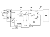
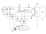
- FIG. 1 is a circuit block diagram showing an example of a step-up AC-DC converter provided with a damage prediction apparatus according to this embodiment.
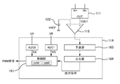
- FIG. 2 is a circuit diagram illustrating an example of a potential difference detection unit used in the damage prediction apparatus according to the present embodiment.
- FIG. 3 is a block diagram illustrating an example of microcomputer hardware used in the damage prediction apparatus according to the present embodiment.
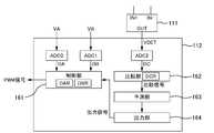
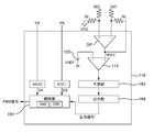
- FIG. 4 is a block diagram illustrating an example of functions realized by the microcomputer used in the damage prediction apparatus according to the present embodiment.
- the AC-DC converter 100 turns on / off a power semiconductor switching element, which will be described later, at a frequency higher than the frequency of the AC voltage when converting the AC voltage into a DC voltage, thereby outputting a DC voltage having a predetermined value. It is a conversion device.
- the AC-DC converter 100 includes a power factor correction circuit.
- An AC-DC converter 100 including a power factor correction circuit includes an AC power supply 101 (for example, a commercial power supply that generates an AC voltage of 50 Hz or 60 Hz), a full-wave rectifier circuit 102, a choke coil 103, a diode 104, a smoothing capacitor 105, a voltage
- the detection resistors 106A and 106B, the current detection resistor 107, the power semiconductor switching element 108, the gate resistor 109 (resistance), the gate driver 110, the potential difference detection circuit 111 (potential difference detection unit), and the microcomputer 112 are configured.
- the damage prediction apparatus includes a gate resistor 109, a gate driver 110, a potential difference detection circuit 111, and a microcomputer 112.
- the full-wave rectifier circuit 102 is a bridge circuit including four diodes 102A to 102D, and outputs a DC voltage obtained by full-wave rectifying an AC voltage generated from the AC power supply 101.
- the choke coil 103 is provided to charge the smoothing capacitor 105 with a DC voltage larger than the DC voltage after full-wave rectification.
- One end of the choke coil 103 is connected to one output end of the full-wave rectifier circuit 102, and a DC current output from the full-wave rectifier circuit 102 is supplied to the choke coil 103.
- the choke coil 103 plays a role of preventing the influence of the ripple current on the smoothing capacitor 105, and further plays a role of making the alternating current input from the alternating current power supply 101 into a sine wave.
- the diode 104 and the smoothing capacitor 105 are connected in series between the other end of the choke coil 103 and the ground GND.
- the voltage detection resistors 106A and 106B are provided for detecting the output voltage of the AC-DC converter 100.
- the voltage detection resistors 106A and 106B are connected in series between the anode of the diode 104 and the ground GND. That is, the series body of the voltage detection resistors 106A and 106B is connected in parallel to both ends of the smoothing capacitor 105 and the load L.
- the current detection resistor 107 is provided to detect the current flowing through the power semiconductor switching element 108 as a voltage.
- the current detection resistor 107 is connected between the other output terminal of the full-wave rectifier circuit 102 and the ground point of the smoothing capacitor 105. Note that the voltage generated at both ends of the current detection resistor 107 is very small.
- the current detection circuit 122 is a circuit that amplifies a minute voltage generated at both ends of the current detection resistor 107 with a predetermined voltage amplification degree.
- the current detection circuit 122 can be realized, for example, by using a known inverting amplifier circuit or differential amplifier circuit. This makes it possible to reliably obtain digital data DB corresponding to a minute voltage generated at both ends of the current detection resistor 107 in the ADC 1 described later.
- the power semiconductor switching element 108 is provided to charge the smoothing capacitor 105 with a DC voltage larger than the DC voltage after full-wave rectification in cooperation with the choke coil 103.
- the power semiconductor switching element 108 has characteristics such as high breakdown voltage, low loss, high efficiency, and high frequency.
- the power semiconductor switching element 108 is assumed to be a GaN-HEMT (High-Electron-Mobility-Transistor), which is a type of GaN (Gallium-Nitride) -FET (Field-Effect-Transistor).
- a GaN-HEMT is an element that uses a two-dimensional electron gas present at the interface of a two-layer heterostructure made of GaN and AlGaN (Gallium Aluminum Nitride) as a current path to increase electron mobility. is there.
- the power semiconductor switching element 108 may be referred to as a GaN-HEMT 108.
- GaN-HEMT is an element that operates normally in principle.
- the GaN-HEMT used in the present embodiment is an element improved so as to operate normally off.
- the gate structure of the GaN-HEMT is changed to have enhanced characteristics, or a low-voltage MOSFET is cascade-connected to the source of the GaN-HEMT.
- Well-known techniques are known.
- the GaN-HEMT used in this embodiment may be realized by any technique.
- the GaN-HEMT 108 in the drawing is represented by one FET symbol.
- the drain of the GaN-HEMT 108 is connected to the other end of the choke coil 103, and the source of the GaN-HEMT 108 is connected to the ground GND.
- the gate of the GaN-HEMT 108 is connected to the gate driver 110 through the gate resistor 109.
- the gate driver 110 is a binary switching signal that becomes a high level (for example, 5 volts) when the GaN-HEMT 108 is turned on and a low level (for example, 0 volts) when the GaN-HEMT 108 is turned off according to an instruction from the microcomputer 112. Is output. That is, the GaN-HEMT 108 is turned on / off according to a change in the level of the switching signal.
- the GaN-HEMT 108 when the GaN-HEMT 108 is provided in the AC-DC converter 100, the following problems may occur due to the large current driving capability (di / dt) of the GaN-HEMT 108.
- resonance occurs when the switching signal output from the gate driver 110 changes to a high level or a low level. This resonance is caused by the inductance component in the circuit wiring of the AC-DC converter 100 and the choke coil 103 and the capacitance component in the circuit wiring of the AC-DC converter 100 and the smoothing capacitor 105.
- ringing having a frequency higher than the frequency of the gate voltage (frequency of the switching signal) is superimposed on the gate voltage applied to the gate of the GaN-HEMT 108.
- the resistance value between the gate and the source of the GaN-HEMT 108 decreases.
- the gate voltage (high level) when the GaN-HEMT 108 is turned on is a constant value, if damage is accumulated in the gate insulating layer of the GaN-HEMT 108, the GaN-HEMT 108 is turned on when the GaN-HEMT 108 is turned on. Current flowing between the gate and source increases. Therefore, an increase in current flowing between the gate and source of the GaN-HEMT 108 flows to the gate resistor 109 as a leakage current.
- a damage prediction apparatus that predicts the degree of damage to the gate insulating layer of the GaN-HEMT 108 by providing attention to the leakage current that flows through the gate resistor 109 when the GaN-HEMT 108 is turned on is provided.
- the potential difference detection circuit 111 shown in FIG. 2 includes a potential V2 (second potential) generated at one end of the gate resistor 109 on the GaN-HEMT 108 side and a potential V1 (first potential) generated at the other end of the gate resistor 109 on the gate driver 110 side.
- This is a circuit that outputs the detection voltage VDET corresponding to the leak current flowing through the gate resistor 109, that is, the detection voltage VDET corresponding to the voltage generated at both ends of the gate resistor 109, by taking in the potential difference V1-V2 with respect to.
- the potential difference detection circuit 111 has a first input terminal IN + to which the potential V1 is input, a second input terminal IN ⁇ to which the potential V2 is input, and an output terminal OUT to which the detection voltage VDET is output. Then, for example, the potential difference detection circuit 111 outputs a differential amplification circuit 111A having a predetermined voltage amplification degree to the first input terminal IN + and the second input so that the detection voltage VDET corresponding to the leak current of a minute value can be output.
- the terminal IN ⁇ and the output terminal OUT are connected to each other.
- the differential amplifier circuit 111A includes an operational amplifier OP, voltage dividing resistors R1 to R4, input resistors R5 and R7, a ground resistor R6, and a feedback resistor R8.
- the voltage dividing resistors R1 and R2 are connected in series between the first input terminal IN + and the ground GND, and the connection point of the voltage dividing resistors R1 and R2 is connected to the first input terminal ( Connected to (+).
- the voltage dividing resistors R3 and R4 are connected in series between the second input terminal IN ⁇ and the ground GND, and the connection point of the voltage dividing resistors R3 and R4 is the second input terminal of the operational amplifier OP via the input resistor R7. (-)It is connected to the.
- the feedback resistor R8 is connected between the second input terminal ( ⁇ ) and the output terminal of the operational amplifier OP.
- the ground resistor R6 is connected between the first input terminal (+) of the operational amplifier OP and the ground GND.
- the voltage at the connection point of the voltage dividing resistors R1 and R2 is Vi +
- the voltage at the connection point of the voltage dividing resistors R3 and R4 is Vi ⁇
- the voltage applied to the first input terminal (+) of the operational amplifier OP is V +
- the voltage at the second input terminal ( ⁇ ) of the operational amplifier OP is V ⁇
- voltage V ⁇ is expressed as in equation (2).
- V + V ⁇
- V o the voltage V o is expressed as shown in Equation (3).
- Vi + and Vi ⁇ are expressed as in the equations (5) and (6).
- the voltage amplification degree of the differential amplifier circuit 111A is determined by (R8 / R7) ⁇ (R2 / (R1 + R2)). Therefore, when a voltage corresponding to the potentials V1 and V2 is applied to the first input terminal (+) and the second input terminal ( ⁇ ) of the operational amplifier OP, it is amplified from the output terminal of the operational amplifier OP at the above voltage amplification degree. The output voltage is output and output from the output terminal OUT as the detection voltage VDET.
- the microcomputer 112 shown in FIG. 3 adjusts the high level period and the low level period of the switching signal with respect to the gate driver 110 so that the detection voltage VA generated at the connection point of the voltage detection resistors 106A and 106B becomes a constant value. Control.
- the microcomputer 112 outputs a PMW signal that triggers when the gate driver 110 outputs a switching signal.
- Each period of the PWM signal is formed by an on period and an off period.
- the on period of the PWM signal corresponds to a high level period of the switching signal
- the off period of the PWM signal corresponds to a low level period of the switching signal.
- the microcomputer 112 adjusts the PWM signal on period short and the PWM signal off period long so that the detection voltage VA becomes a constant value.
- the microcomputer 112 adjusts the PWM signal on period longer and the PWM signal off period shorter so that the detection voltage VA becomes a constant value.
- the ON period and the OFF period of the first PWM signal output from the microcomputer 112 may have a relation that the ON period is shorter than the OFF period and the duty is less than 50%, for example. Further, the duty period may be 50% or more longer than the off period.
- the microcomputer 112 performs the power factor correction operation so that the AC current of the AC power supply 101 becomes a sine wave and the detection voltage VB output from the current detection circuit 122 becomes a sine wave full-wave rectified waveform. Control.
- the microcomputer 112 compares the detection voltage VDET with the reference voltage VREF, and predicts that predetermined damage is accumulated in the gate insulating layer of the GaN-HEMT 108 when the detection voltage VDET exceeds the reference voltage VREF. Control.
- the microcomputer 112 includes a ROM 151, a CPU 152, a RAM 153, an I / O port group 154, an AD converter group 155, and a bus 156.
- the ROM 151 is configured by a nonvolatile memory such as a mask ROM or a flash ROM.
- the ROM 151 stores a program for performing the above control in advance.
- the RAM 153 includes a volatile memory that can write and read data during a period in which power for the RAM 153 is supplied. In the RAM 153, data obtained by the CPU 152 executing the program is written. On the other hand, data necessary for the CPU 152 to execute the program is read from the RAM 153.
- the I / O port group 154 inputs or outputs data necessary when the CPU 152 executes a program.
- the A / D converter group 155 takes in analog data required when the CPU 152 executes a program from the outside and converts it into digital data.
- the CPU 152 is necessary for data read from the RAM 153, data input to the I / O port group 154, data output from the A / D converter group 155, etc., in accordance with the contents of the program read from the ROM 151. Performs proper calculation processing. Note that the ROM 151, CPU 152, RAM 153, I / O port group 154, and A / D converter group 155 are connected via a bus 156.
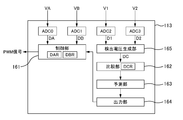
- the microcomputer 112 shown in FIG. 4 includes ADCs 0 to ADC2 as the AD converter group 155, a control unit 161, a comparison unit 162, a prediction unit 163, and an output unit 164.
- the control unit 161, the comparison unit 162, the prediction unit 163, and the output unit 164 are functions realized by the CPU 152 reading out a program from the ROM 151 and executing the program.
- ADC0 takes in the detection voltage VA generated at the connection point of the voltage detection resistors 106A and 106B and converts it into digital data DA.
- the ADC 1 takes in the detection voltage VB output from the current detection circuit 122 and converts it into digital data DB.
- the ADC 2 takes in the detection voltage VDET corresponding to the leak current flowing through the gate resistor 109 and converts it into digital data DC.
- the control unit 161 stores in advance the reference digital data DAR that is the same as the conversion result of the ADC 0 when the detection voltage VA is a constant value. Then, the control unit 161 compares the digital data DA with the reference digital data DAR. For example, when the digital data DA is larger than the reference digital data DAR, the control unit 161 adjusts the on period of the PWM signal short and lengthens the off period of the PWM signal so that the digital data DA approaches the reference digital data DAR. Adjust and output the PWM signal after adjustment.
- control unit 161 adjusts the PWM signal ON period longer and shortens the PWM signal OFF period so that the digital data DA approaches the reference digital data DAR. Adjust and output the PWM signal after adjustment.
- control unit 161 has a reference digital data DBR indicating a sine wave full-wave rectified waveform having a predetermined amplitude and frequency so that control for the power factor improving operation of the AC-DC converter 100 can be performed. Is stored in the lookup table. Then, the control unit 161 takes in the digital data DB and reads out the reference digital data DBR so that the AC current of the AC power supply 101 becomes a sine wave, and the detection voltage VB output from the current detection circuit 122 is a sine wave. The control for the power factor correction operation is performed so that the full-wave rectified waveform is obtained.
- the comparison unit 162 compares the detection voltage VDET corresponding to the leakage current flowing through the gate resistor 109 with the reference voltage VREF. Since the comparison unit 162 is a function realized by software processing of the microcomputer 112, the comparison unit 162 compares the digital data DC indicating the detection voltage VDET with the reference digital data DCR indicating the reference voltage VREF. The comparison unit 162 stores digital data DCR in advance as a value indicating that predetermined damage has accumulated in the gate insulating layer of the GaN-HEMT 108.
- the comparison unit 162 When the digital data DC does not exceed the reference digital data DCR, the comparison unit 162 outputs a comparison signal of one level (for example, low level), and when the digital data DC exceeds the reference digital data DCR, the other level A comparison signal (for example, high level) is output.
- one level for example, low level
- the other level A comparison signal for example, high level
- the prediction unit 163 monitors the level of the comparison signal output from the comparison unit 162 in order to predict whether or not predetermined damage has accumulated in the gate insulating layer of the GaN-HEMT 108. Then, when the comparison signal changes from one level to the other level, the prediction unit 163 predicts that predetermined damage is accumulated in the gate insulating layer of the GaN-HEMT 108.
- the output unit 164 is arranged in accordance with a prediction result indicating that predetermined damage is accumulated in the gate insulating layer of the GaN-HEMT 108 in order to prevent a trouble of the AC-DC converter 100 due to destruction of the GaN-HEMT 108.
- An output signal of a level (for example, high level) is output.
- the control unit 161 stops outputting the PWM signal when the output signal becomes one level. As a result, the switching operation (periodic on / off operation) of the GaN-HEMT 108 is stopped, and it is possible to prevent a trouble of the AC-DC converter 100 due to the destruction of the GaN-HEMT 108. Further, when the output signal becomes one level, the control unit 161 displays a prediction result indicating that predetermined damage has accumulated in the gate insulating layer of the GaN-HEMT 108 as a monitor monitor (not shown) or a speaker (not shown). The program of the ROM 151 may be modified so as to warn the administrator of the AC-DC converter 100 through
- the GaN-HEMT 108 When the GaN-HEMT 108 is turned off, the excitation energy of the choke coil 103 is released to the smoothing capacitor 105 via the diode 104.
- the GaN-HEMT 108 When the GaN-HEMT 108 is turned on / off, the on period and the off period of the PWM signal are adjusted so that the detection voltage VA approaches a constant value. In this way, when the on / off operation of the GaN-HEMT 108 is repeated, a DC voltage larger than the DC voltage after full-wave rectification (DC voltage obtained by boosting the DC voltage after full-wave rectification) is applied to the smoothing capacitor 105. It will be charged.
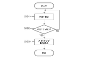
- FIG. 5 is a waveform diagram for explaining the operation of the damage prediction apparatus according to the present embodiment.
- FIG. 5 schematically shows the waveform until the detection voltage VDET exceeds the reference voltage VREF in the process in which damage is accumulated in the gate insulating layer of the GaN-HEMT 108.
- FIG. 6 is a flowchart for explaining the operation of the damage prediction apparatus according to the present embodiment. The main body that executes the operation of FIG.
- the ADC 2 samples the detection voltage VDET at a timing intermediate between the high level periods in the switching signal, for example.
- the detection voltage VDET is taken in and converted into digital data DC. Note that when the sampling timing in the ADC 2 is set to a timing that is the middle of the high level period in the switching signal, for example, a signal with a duty of 50% is generated with the high level period of the PWM signal synchronized with the switching signal as one cycle.
- the change timing of the signal may be used (S101).
- the comparison unit 162 compares the digital data DC indicating the detection voltage VDET with the reference digital data DCR indicating the reference voltage VREF (S102).
- the comparison unit 162 outputs a low level comparison signal, for example.
- the above S101 is executed again, and the ADC 2 outputs the next digital data DC.
- the comparison unit 162 outputs a high level comparison signal, for example.
- the prediction unit 163 predicts that predetermined damage is accumulated in the gate insulating layer of the GaN-HEMT 108.
- the output unit 164 outputs, for example, a high-level output signal when a result (for example, a flag value) predicted to have accumulated predetermined damage in the gate insulating layer of the GaN-HEMT 108 is input.
- the control unit 161 stops outputting the PWM signal in order to stop the switching operation of the GaN-HEMT 108 (S103).
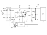
- FIG. 7 is a circuit block diagram showing an example of a step-up DC-DC converter provided with the damage prediction apparatus according to the present embodiment.
- FIG. 8 is a block diagram illustrating an example of functions of a microcomputer used in the damage prediction apparatus according to the present embodiment.
- FIG. 7 Note that the same components as those of the AC-DC converter 100 are denoted by the same reference numerals and description thereof is omitted.
- a DC-DC converter 700 shown in FIG. 7 turns on / off the GaN-HEMT 108 at the same frequency as the AC-DC converter 100 when converting a DC voltage into a DC voltage larger than the DC voltage. This is a power converter that outputs a direct current voltage.
- the DC-DC converter 700 differs from the AC-DC converter 100 in that it includes a DC power supply 123 instead of the AC power supply 101 and the full-wave rectifier circuit 102 and does not include the current detection resistor 107 and the current detection circuit 122. Yes.
- the damage prediction apparatus includes a gate resistor 109, a gate driver 110, a potential difference detection circuit 111, and a microcomputer 124.
- control unit 166 differs from the microcomputer 112 in that the microcomputer 124 does not include the ADC 1. Further, the control unit 166 is different from the control unit 161 in that the reference digital data DBR is not stored. That is, the control unit 166 compares the digital data DA output from the ADC 0 with the reference digital data DAR, and sets the ON period so that the detection voltage VA generated at the connection point of the voltage detection resistors 106A and 106B approaches a constant value. Only the PWM signal adjusted in the off period is output.
- FIG. 9 is a circuit block diagram showing an example of a step-up AC-DC converter provided with the damage prediction apparatus according to the present embodiment.
- FIG. 10 is a block diagram illustrating an example of functions realized by a microcomputer used in the damage prediction apparatus according to the present embodiment.
- the AC-DC converter 200 shown in FIG. 9 does not include the potential difference detection circuit 111, but generates digital data DC corresponding to the detection voltage VREF from the potentials V1 and V2 generated at both ends of the gate resistor 109 by software processing of the microcomputer 113. This is different from the AC-DC converter 100.
- the damage prediction apparatus includes a gate resistor 109, a gate driver 110, and a microcomputer 113.
- a DC power supply 123 may be provided instead of the AC power supply 101 and the full-wave rectifier circuit 102.
- the 10 is different from the microcomputer 112 in that the ADC 113 as the AD converter group 155 and a detection voltage generation unit 165 are newly provided.
- the detection voltage generation unit 165 is a function realized by the CPU 152 reading a program from the ROM 151 and executing it.
- the AC-DC converter 200 is used as a DC-DC converter, the ADC 1 to which the detection voltage VB is input and the reference digital data DBR stored in the control unit 166 are not necessary.
- ADC 2 takes in the potential V 1 generated at the other end of the gate resistor 109 and converts it into digital data D 1.
- the ADC 2 samples the potential V1 at a timing that is the middle of the high-level period in the switching signal, takes in the sampled potential V1, and converts it into digital data D1.
- the ADC 3 takes in the potential V2 generated at one end of the gate resistor 109 and converts it into digital data D2.
- the ADC 3 samples the potential V2 at the same timing as the sampling timing in the ADC 2, takes in the sampled potential V2, and converts it into digital data D2.
- the detection voltage generation unit 165 generates digital data DC corresponding to the detection voltage VREF by performing a subtraction process on the digital data D1 and D2, and outputs the digital data DC to the comparison unit 162.
- the processing until the output of the PWM signal is stopped according to the comparison result of the comparison unit 162 is the same as that of the microcomputer 112.
- FIG. 11 is a circuit block diagram showing an example of a step-up AC-DC converter provided with the damage prediction apparatus according to the present embodiment.
- FIG. 12 is a block diagram illustrating an example of functions realized by a microcomputer used in the damage prediction apparatus according to the present embodiment.
- the AC-DC converter 300 shown in FIG. 11 includes an output terminal OUT of the potential difference detection circuit 111 and a GPIO (General Purpose Input / Output) functioning as a general-purpose I / O port in the I / O port group 154 of the microcomputer 114. It differs from the AC-DC converter 100 in that a comparator 115 is provided therebetween.
- the damage prediction apparatus includes a gate resistor 109, a gate driver 110, a potential difference detection circuit 111, a microcomputer 114, and a comparator 115.
- a DC power source 123 may be provided instead of the AC power source 101 and the full-wave rectifier circuit 102.
- the microcomputer 12 differs from the microcomputer 112 in that the microcomputer 114 does not include the ADC 2 and the comparison unit 162.
- the AC-DC converter 300 is used as a DC-DC converter, the ADC 1 to which the detection voltage VB is input and the reference digital data DBR stored in the control unit 166 are not necessary.
- the detection voltage VDET output from the output terminal OUT of the potential difference detection circuit 111 is applied to the first input terminal (+) of the comparator 115.
- the reference voltage VREF generated from the DC power supply 116 is applied to the second input terminal ( ⁇ ) of the comparator 115.
- the reference voltage VREF is the same voltage as the detection voltage VDET when a predetermined damage is accumulated in the gate insulating layer of the GaN-HEMT 108.
- the comparator 115 outputs a high-level comparison signal indicating that predetermined damage has accumulated in the gate insulating layer of the GaN-HEMT 108.
- the comparison signal is input to the prediction unit 163 through GPIO.
- the processing until the output of the PWM signal is stopped according to the prediction result of the prediction unit 163 is the same as that of the microcomputer 112.
- FIG. 13 is a circuit block diagram showing an example of a step-up AC-DC converter provided with the damage prediction apparatus according to the present embodiment.
- FIG. 14 is a block diagram illustrating an example of functions of a microcomputer used in the damage prediction apparatus according to the present embodiment.
- the damage prediction apparatus includes a gate resistor 109, a gate driver 110, voltage dividing resistors R1 to R4, input resistors R5 and R7, a feedback resistor R8, a ground resistor R6, and a microcomputer 116.
- a DC power supply 123 may be provided instead of the AC power supply 101 and the full-wave rectifier circuit 102.
- the microcomputer 116 shown in FIG. Therefore, the ADC 1 and the reference digital data DBR stored in the control unit 166 are not necessary.
- the voltage dividing resistors R1 and R2 are connected in series between one end of the gate resistor 109 and the ground GND, and the connection point of the voltage dividing resistors R1 and R2 is connected to the first input terminal ( Connected to (+).
- the voltage dividing resistors R3 and R4 are connected in series between the other end of the gate resistor 109 and the ground GND, and the connection point of the voltage dividing resistors R3 and R4 is the second input terminal of the operational amplifier OP via the input resistor R7. (-)It is connected to the.
- the feedback resistor R8 is connected between the second input terminal ( ⁇ ) and the output terminal of the operational amplifier OP.
- the ground resistor R6 is connected between the first input terminal (+) of the operational amplifier OP and the ground GND.
- FIG. 15 is a circuit block diagram showing an example of a step-up AC-DC converter provided with the damage prediction apparatus according to the present embodiment.
- FIG. 16 is a block diagram illustrating an example of functions of the microcomputer used in the damage prediction apparatus according to the present embodiment.
- the damage prediction apparatus includes a gate resistor 117, a switch 118, a DC power source 119, a potential difference detection circuit 111, and a microcomputer 120.
- a DC power source 123 may be provided instead of the AC power source 101 and the full-wave rectifier circuit 102.
- the control unit 16 is different from the microcomputer 112 in that an ON signal for turning on the switch 118 for a certain period is output from the control unit 161.
- the AC-DC converter 500 is used as a DC-DC converter, the ADC 1 to which the detection voltage VB is input and the reference digital data DBR stored in the control unit 166 are not necessary.
- the switch 118 is connected between the gate of the GaN-HEMT 108 and one end of the gate resistor 117.
- the DC power source 119 is connected between the other end of the gate resistor 117 and the ground GND.
- the switch 118 is turned on for a certain period in response to an ON signal output from the control unit 161 of the microcomputer 120 during standby before the AC-DC converter 500 starts an operation of converting an AC voltage into a DC voltage.
- the switch 118 is turned on for a certain period according to the ON signal.
- the resistance value between the gate and the source of the GaN-HEMT 108 decreases, so that a leak current flows through the gate resistor 117.
- the potential V1 and the potential V2 generated at both ends of the gate resistor 117 are input to the first input terminal IN + and the second input terminal IN ⁇ of the potential difference detection circuit 111, respectively.
- the processing until the output of the PWM signal is stopped according to the detection voltage VDET output from the potential difference detection circuit 111 is the same as that of the microcomputer 112.
- the gate resistor 109 has a role of suppressing ringing noise superimposed on the gate voltage. Therefore, as shown in the first to fifth embodiments, when the gate resistor 109 is also used as a resistor for obtaining the detection voltage VDET, there is a restriction in setting the resistance value of the gate resistor 109.
- the gate resistor 117 is a resistor for obtaining the detection voltage VDET.
- the resistance value of the gate resistor 117 can be set to a value at which an optimum detection voltage VDET can be obtained.
- the switch 118 is a transistor element such as a MOS-FET.
- FIG. 17 is a circuit block diagram showing an example of a step-up AC-DC converter provided with the damage prediction apparatus according to the present embodiment.
- FIG. 18 is a block diagram illustrating an example of functions of a microcomputer used in the damage prediction apparatus according to the present embodiment.
- the AC-DC converter 600 shown in FIG. 17 does not include the potential difference detection circuit 111, and generates digital data DC corresponding to the detection voltage VREF from the potentials V1 and V2 generated at both ends of the gate resistor 117 by software processing of the microcomputer 121. This is different from the AC-DC converter 500.
- the damage prediction apparatus includes a gate resistor 117, a switch 118, a DC power source 119, and a microcomputer 121.
- a DC power source 123 may be provided instead of the AC power source 101 and the full-wave rectifier circuit 102.
- the microcomputer 121 shown in FIG. 18 is different from the microcomputer 113 in that the controller 161 outputs an ON signal for turning on the switch 118 for a certain period.
- the AC-DC converter 600 is used as a DC-DC converter, the ADC 1 to which the detection voltage VB is input and the reference digital data DBR stored in the control unit 166 are not necessary.
- the switch 118 is turned on for a certain period in response to an ON signal output from the control unit 161 of the microcomputer 121 during standby before the AC-DC converter 600 starts an operation of converting an AC voltage into a DC voltage.
- the switch 118 is turned on for a certain period according to the ON signal.
- the resistance value between the gate and the source of the GaN-HEMT 108 decreases, so that a leak current flows through the gate resistor 117.
- the potential V1 and the potential V2 generated at both ends of the gate resistor 117 are input to ADC2 and ADC3, respectively.
- the processing until the output of the PWM signal is stopped in accordance with the digital data D1 and D2 output from the ADC2 and ADC3, respectively, is the same as that of the microcomputer 113.
- the damage prediction apparatus it is possible to predict the destruction of the GaN-HEMT 108 and prevent troubles in the AC-DC converters 100 to 600 and the DC-DC converters 700 to 1200.
- an FET, MOSFET, or IGBT made of SiC silicon carbide
- SiC silicon carbide
- the damage prediction apparatus described in the first to seventh embodiments is not limited to a step-up AC-DC converter and a DC-DC converter, but a step-down AC-DC converter, a DC-DC converter, Can also be used to predict damage to the gate insulating layer of the power semiconductor switching element in the inverter.
Landscapes
- Engineering & Computer Science (AREA)
- Power Engineering (AREA)
- Physics & Mathematics (AREA)
- General Physics & Mathematics (AREA)
- Microelectronics & Electronic Packaging (AREA)
- Dc-Dc Converters (AREA)
- Rectifiers (AREA)
- Power Conversion In General (AREA)
- Testing Of Individual Semiconductor Devices (AREA)
- Inverter Devices (AREA)
Abstract
According to the present invention, a damage determination apparatus for a power semiconductor switching element is provided with: a resistor that is connected to the gate of the power semiconductor switching element; a comparison unit that compares a reference voltage with a detected voltage in accordance with the voltage generated at both ends of the resistor, when a prescribed voltage is applied to the gate of the power semiconductor switching element; and a prediction unit that predicts that a prescribed damage has accumulated in the gate insulating layer of the power semiconductor switching element when the detected voltage exceeds the reference voltage.
Description
本発明は、パワー半導体スイッチング素子のダメージ予測装置及びダメージ予測方法、AC-DCコンバータ、DC-DCコンバータに関する。
The present invention relates to a power semiconductor switching element damage prediction apparatus and damage prediction method, an AC-DC converter, and a DC-DC converter.
交流電圧を直流電圧に変換する際にパワー半導体スイッチング素子を周期的にオン/オフすることによって所定値の直流電圧を出力するAC-DCコンバータや、直流電圧を当該直流電圧とは異なる値の直流電圧に変換する際にパワー半導体スイッチング素子を周期的にオン/オフすることによって所定値の直流電圧を出力するDC-DCコンバータ等の電力変換装置が知られている。
An AC-DC converter that outputs a DC voltage of a predetermined value by periodically turning on and off the power semiconductor switching element when converting the AC voltage to a DC voltage, or a DC voltage that is different from the DC voltage. 2. Description of the Related Art A power conversion device such as a DC-DC converter that outputs a DC voltage of a predetermined value by periodically turning on / off a power semiconductor switching element when converting to a voltage is known.
上記の電力変換装置に対して、例えば、GaN(窒化ガリウム:Gallium Nitride)からなるFET(電界効果トランジスタ:Field Effect Transistor)(以下、GaN-FETと称する)、SiC(炭化ケイ素:Silicon Carbide)からなるFET(以下、SiC-FETと称する)、IGBT(絶縁ゲート型バイポーラトランジスタ:Insulated Gate Bipolar Transistor)等のパワー半導体スイッチング素子を用いる場合がある。
For the above power conversion device, for example, from FET (Field Effect Transistor) (hereinafter referred to as GaN-FET) made of GaN (Gallium Nitride), SiC (Silicon Carbide). In some cases, power semiconductor switching elements such as FETs (hereinafter referred to as SiC-FETs) and IGBTs (Insulated Gate Bipolar Transistors) are used.
しかし、上記の電力変換装置に対してこれらのパワー半導体スイッチング素子を用いた場合、パワー半導体スイッチング素子の電流駆動能力(di/dt)が大きいことに起因して、以下の問題を生じる虞がある。例えば、パワー半導体スイッチング素子を周期的にオン/オフする際にパワー半導体スイッチング素子のゲートに印加されるゲート電圧がハイレベルとローレベルのうち何れか一方のレベルから他方のレベルへ変化すると、AC-DCコンバータやDC-DCコンバータの回路配線に寄生するインダクタンス成分及びキャパシタンス成分等の共振に伴って、ゲート電圧に対して当該ゲート電圧の周波数よりも高い周波数を有するリンギングが重畳することとなる。つまり、ゲート電圧に対してオーバーシュートとアンダーシュートが現れることとなる。このようにして、ゲート電圧が定格電圧を超えてしまうと、パワー半導体スイッチング素子のゲート絶縁層にダメージが徐々に蓄積され、やがてパワー半導体スイッチング素子の破壊に至る虞がある。
However, when these power semiconductor switching elements are used for the above power converter, the following problems may occur due to the large current driving capability (di / dt) of the power semiconductor switching elements. . For example, when the gate voltage applied to the gate of the power semiconductor switching element when the power semiconductor switching element is periodically turned on / off changes from one of the high level and the low level to the other level, AC -Ringing having a frequency higher than the frequency of the gate voltage is superimposed on the gate voltage due to resonance of inductance components and capacitance components parasitic on the circuit wiring of the DC converter or DC-DC converter. That is, overshoot and undershoot appear with respect to the gate voltage. Thus, when the gate voltage exceeds the rated voltage, damage is gradually accumulated in the gate insulating layer of the power semiconductor switching element, and there is a possibility that the power semiconductor switching element is eventually destroyed.
例えば、特許文献1の場合、パワー半導体スイッチング素子のゲート電圧値を検出しているが、これは、パワー半導体スイッチング素子におけるスイッチング損失及びノイズの低減を図るためであって、パワー半導体スイッチング素子のゲート絶縁層に蓄積されたダメージの程度を予測するためではない。
For example, in the case of Patent Document 1, the gate voltage value of the power semiconductor switching element is detected. This is to reduce switching loss and noise in the power semiconductor switching element. It is not for predicting the degree of damage accumulated in the insulating layer.
そこで、本発明は、パワー半導体スイッチング素子のゲート絶縁層に蓄積されたダメージの程度の予測を可能にするダメージ予測装置、ダメージ予測方法、AC-DCコンバータ、DC-DCコンバータを提供することを目的とする。
Accordingly, the present invention provides a damage prediction apparatus, a damage prediction method, an AC-DC converter, and a DC-DC converter that can predict the degree of damage accumulated in a gate insulating layer of a power semiconductor switching element. And
前述した課題を解決する主たる本発明は、パワー半導体スイッチング素子のダメージ予測装置であって、前記パワー半導体スイッチング素子のゲートに接続される抵抗と、前記パワー半導体スイッチング素子のゲートに所定電圧が印加されると、前記抵抗の両端に生じる電圧に応じた検出電圧と基準電圧とを比較する比較部と、前記検出電圧が前記基準電圧を超えると、前記パワー半導体スイッチング素子のゲート絶縁層に所定のダメージが蓄積されたものと予測する予測部と、を備えてなる。
The main present invention for solving the above-described problem is a power semiconductor switching element damage prediction apparatus, wherein a resistor connected to a gate of the power semiconductor switching element and a predetermined voltage is applied to the gate of the power semiconductor switching element. Then, a comparison unit that compares a detection voltage according to a voltage generated at both ends of the resistor and a reference voltage, and when the detection voltage exceeds the reference voltage, predetermined damage is caused to the gate insulating layer of the power semiconductor switching element. A predicting unit that predicts that is stored.
本発明の他の特徴については、添付図面及び本明細書の記載により明らかとなる。
Other features of the present invention will become apparent from the accompanying drawings and the description of the present specification.
本発明によれば、パワー半導体スイッチング素子のゲート絶縁層に蓄積されたダメージの程度を予測し、パワー半導体スイッチング素子の破壊に伴うトラブルを未然に防止することが可能になる。
According to the present invention, it is possible to predict the degree of damage accumulated in the gate insulating layer of the power semiconductor switching element, and to prevent troubles associated with destruction of the power semiconductor switching element.
本明細書および添付図面の記載により、少なくとも以下の事項が明らかとなる。
===第1実施形態=== At least the following matters will become apparent from the description of this specification and the accompanying drawings.
=== First Embodiment ===
===第1実施形態=== At least the following matters will become apparent from the description of this specification and the accompanying drawings.
=== First Embodiment ===
<<AC-DCコンバータの構成>>
図1は、本実施形態に係るダメージ予測装置を備えた昇圧型のAC-DCコンバータの一例を示す回路ブロック図である。図2は、本実施形態に係るダメージ予測装置に用いられる電位差検出部の一例を示す回路図である。図3は、本実施形態に係るダメージ予測装置に用いられるマイコンのハードウエアの一例を示すブロック図である。図4は、本実施形態に係るダメージ予測装置に用いられるマイコンによって実現される機能の一例を示すブロック図である。 << Configuration of AC-DC converter >>
FIG. 1 is a circuit block diagram showing an example of a step-up AC-DC converter provided with a damage prediction apparatus according to this embodiment. FIG. 2 is a circuit diagram illustrating an example of a potential difference detection unit used in the damage prediction apparatus according to the present embodiment. FIG. 3 is a block diagram illustrating an example of microcomputer hardware used in the damage prediction apparatus according to the present embodiment. FIG. 4 is a block diagram illustrating an example of functions realized by the microcomputer used in the damage prediction apparatus according to the present embodiment.
以下、図1~図4を参照しつつ、本実施形態に係るダメージ予測装置を備えたAC-DCコンバータの構成について説明する。
Hereinafter, the configuration of the AC-DC converter including the damage prediction apparatus according to the present embodiment will be described with reference to FIGS.
AC-DCコンバータ100は、交流電圧を直流電圧に変換する際に、後述するパワー半導体スイッチング素子を交流電圧の周波数よりも高い周波数でオン/オフすることによって、所定値の直流電圧を出力する電力変換装置である。尚、AC-DCコンバータ100は、力率改善回路を備えている。
The AC-DC converter 100 turns on / off a power semiconductor switching element, which will be described later, at a frequency higher than the frequency of the AC voltage when converting the AC voltage into a DC voltage, thereby outputting a DC voltage having a predetermined value. It is a conversion device. The AC-DC converter 100 includes a power factor correction circuit.
力率改善回路を備えたAC-DCコンバータ100は、交流電源101(例えば50Hz又は60Hzの交流電圧を発生する商用電源)、全波整流回路102、チョークコイル103、ダイオード104、平滑コンデンサ105、電圧検出抵抗106A,106B、電流検出抵抗107、パワー半導体スイッチング素子108、ゲート抵抗109(抵抗)、ゲートドライバ110、電位差検出回路111(電位差検出部)、マイコン112を含んで構成されている。尚、ダメージ予測装置は、ゲート抵抗109、ゲートドライバ110、電位差検出回路111、マイコン112を含んで構成されている。
An AC-DC converter 100 including a power factor correction circuit includes an AC power supply 101 (for example, a commercial power supply that generates an AC voltage of 50 Hz or 60 Hz), a full-wave rectifier circuit 102, a choke coil 103, a diode 104, a smoothing capacitor 105, a voltage The detection resistors 106A and 106B, the current detection resistor 107, the power semiconductor switching element 108, the gate resistor 109 (resistance), the gate driver 110, the potential difference detection circuit 111 (potential difference detection unit), and the microcomputer 112 are configured. The damage prediction apparatus includes a gate resistor 109, a gate driver 110, a potential difference detection circuit 111, and a microcomputer 112.
全波整流回路102は、4個のダイオード102A~102Dからなるブリッジ回路であって、交流電源101から発生する交流電圧を全波整流した直流電圧を出力する。
The full-wave rectifier circuit 102 is a bridge circuit including four diodes 102A to 102D, and outputs a DC voltage obtained by full-wave rectifying an AC voltage generated from the AC power supply 101.
チョークコイル103は、全波整流後の直流電圧よりも大きい直流電圧を平滑コンデンサ105に充電するために設けられている。チョークコイル103の一端は全波整流回路102の一方の出力端に接続され、チョークコイル103には全波整流回路102から出力された直流電流が供給される。尚、チョークコイル103は、平滑コンデンサ105に対するリップル電流の影響を防止する役割も果たし、更には、交流電源101から入力される交流電流を正弦波とする役割も果たしている。
The choke coil 103 is provided to charge the smoothing capacitor 105 with a DC voltage larger than the DC voltage after full-wave rectification. One end of the choke coil 103 is connected to one output end of the full-wave rectifier circuit 102, and a DC current output from the full-wave rectifier circuit 102 is supplied to the choke coil 103. The choke coil 103 plays a role of preventing the influence of the ripple current on the smoothing capacitor 105, and further plays a role of making the alternating current input from the alternating current power supply 101 into a sine wave.
ダイオード104及び平滑コンデンサ105は、チョークコイル103の他端と接地GNDとの間に直列接続されている。
The diode 104 and the smoothing capacitor 105 are connected in series between the other end of the choke coil 103 and the ground GND.
電圧検出抵抗106A,106Bは、AC-DCコンバータ100の出力電圧を検出するために設けられている。電圧検出抵抗106A,106Bは、ダイオード104のアノードと接地GNDとの間に直列接続されている。つまり、電圧検出抵抗106A,106Bの直列体は、平滑コンデンサ105の両端と負荷Lとに並列接続されている。
The voltage detection resistors 106A and 106B are provided for detecting the output voltage of the AC-DC converter 100. The voltage detection resistors 106A and 106B are connected in series between the anode of the diode 104 and the ground GND. That is, the series body of the voltage detection resistors 106A and 106B is connected in parallel to both ends of the smoothing capacitor 105 and the load L.
電流検出抵抗107は、パワー半導体スイッチング素子108に流れる電流を電圧として検出するために設けられている。電流検出抵抗107は、全波整流回路102の他方の出力端と平滑コンデンサ105の接地点との間に接続されている。尚、電流検出抵抗107の両端に発生する電圧は微小である。
The current detection resistor 107 is provided to detect the current flowing through the power semiconductor switching element 108 as a voltage. The current detection resistor 107 is connected between the other output terminal of the full-wave rectifier circuit 102 and the ground point of the smoothing capacitor 105. Note that the voltage generated at both ends of the current detection resistor 107 is very small.
電流検出回路122は、電流検出抵抗107の両端に発生する微小な電圧を所定の電圧増幅度で増幅する回路である。電流検出回路122は、例えば、周知の反転増幅回路や差動増幅回路を用いることによって実現することが可能である。これによって、後述するADC1において、電流検出抵抗107の両端に発生する微小な電圧に相当するデジタルデータDBを確実に得ることが可能になる。
The current detection circuit 122 is a circuit that amplifies a minute voltage generated at both ends of the current detection resistor 107 with a predetermined voltage amplification degree. The current detection circuit 122 can be realized, for example, by using a known inverting amplifier circuit or differential amplifier circuit. This makes it possible to reliably obtain digital data DB corresponding to a minute voltage generated at both ends of the current detection resistor 107 in the ADC 1 described later.
パワー半導体スイッチング素子108は、チョークコイル103と協働して、全波整流後の直流電圧よりも大きい直流電圧を平滑コンデンサ105に充電するために設けられている。本実施形態の場合、パワー半導体スイッチング素子108は、高耐圧、低損失、高効率、高周波等の特性を備えている。例えば、パワー半導体スイッチング素子108は、GaN(窒化ガリウム:Gallium Nitride)-FET(電界効果トランジスタ:Field Effect Transistor)の一種であるGaN-HEMT(High Electron Mobility Transistor)であることとする。GaN-HEMTは、GaNとAlGaN(窒化アルミニウムガリウム:Gallium Aluminum Nitride) とからなる2層のヘテロ構造の界面に存在する2次元電子ガスを電子の移動度を高めるために電流の経路として用いる素子である。以下、説明の便宜上、パワー半導体スイッチング素子108をGaN-HEMT108と称する場合がある。
The power semiconductor switching element 108 is provided to charge the smoothing capacitor 105 with a DC voltage larger than the DC voltage after full-wave rectification in cooperation with the choke coil 103. In the case of this embodiment, the power semiconductor switching element 108 has characteristics such as high breakdown voltage, low loss, high efficiency, and high frequency. For example, the power semiconductor switching element 108 is assumed to be a GaN-HEMT (High-Electron-Mobility-Transistor), which is a type of GaN (Gallium-Nitride) -FET (Field-Effect-Transistor). A GaN-HEMT is an element that uses a two-dimensional electron gas present at the interface of a two-layer heterostructure made of GaN and AlGaN (Gallium Aluminum Nitride) as a current path to increase electron mobility. is there. Hereinafter, for convenience of description, the power semiconductor switching element 108 may be referred to as a GaN-HEMT 108.
GaN-HEMTは、原理的にはノーマリオンで動作する素子である。しかし、本実施形態に用いられるGaN-HEMTは、ノーマリオフで動作するように改良された素子であることとする。GaN-HEMTをノーマリオフで動作するように改良する技術として、GaN-HEMTのゲート構造をエンハンス特性となるように変更したり、GaN-HEMTのソースに対して低耐圧のMOSFETをカスケード接続したりする周知の技術が知られている。本実施形態に用いられるGaN-HEMTは、何れの技術によって実現されたものでもよい。尚、説明の便宜上、図面におけるGaN-HEMT108を1個のFETのシンボルで表すこととする。
GaN-HEMT is an element that operates normally in principle. However, the GaN-HEMT used in the present embodiment is an element improved so as to operate normally off. As a technique for improving the GaN-HEMT so that it operates normally off, the gate structure of the GaN-HEMT is changed to have enhanced characteristics, or a low-voltage MOSFET is cascade-connected to the source of the GaN-HEMT. Well-known techniques are known. The GaN-HEMT used in this embodiment may be realized by any technique. For convenience of explanation, the GaN-HEMT 108 in the drawing is represented by one FET symbol.
GaN-HEMT108のドレインはチョークコイル103の他端に接続され、GaN-HEMT108のソースは接地GNDに接続されている。又、GaN-HEMT108のゲートはゲート抵抗109を介してゲートドライバ110に接続されている。
The drain of the GaN-HEMT 108 is connected to the other end of the choke coil 103, and the source of the GaN-HEMT 108 is connected to the ground GND. The gate of the GaN-HEMT 108 is connected to the gate driver 110 through the gate resistor 109.
ゲートドライバ110は、マイコン112からの指示に従って、GaN-HEMT108をオンするときにハイレベル(例えば5ボルト)、GaN-HEMT108をオフするときにローレベル(例えば0ボルト)となる2値のスイッチング信号を出力する。つまり、GaN-HEMT108は、スイッチング信号のレベルの変化に応じてオン/オフする。
The gate driver 110 is a binary switching signal that becomes a high level (for example, 5 volts) when the GaN-HEMT 108 is turned on and a low level (for example, 0 volts) when the GaN-HEMT 108 is turned off according to an instruction from the microcomputer 112. Is output. That is, the GaN-HEMT 108 is turned on / off according to a change in the level of the switching signal.
ここで、AC-DCコンバータ100にGaN-HEMT108を設けた場合、GaN-HEMT108の電流駆動能力(di/dt)が大きいことに起因して、以下の問題を生じる虞がある。例えば、ゲートドライバ110から出力されるスイッチング信号がハイレベル又はローレベルに変化すると共振が生じる。この共振は、AC-DCコンバータ100の回路配線やチョークコイル103におけるインダクタンス成分と、AC-DCコンバータ100の回路配線や平滑コンデンサ105におけるキャパシタンス成分と、によって生じる。この共振が生じると、GaN-HEMT108のゲートに印加されるゲート電圧に対して、ゲート電圧の周波数(スイッチング信号の周波数)よりも高い周波数を有するリンギングが重畳する。つまり、スイッチング信号がハイレベルに変化すると、ゲート電圧にオーバーシュートが現れ、一方、スイッチング信号がローレベルに変化すると、ゲート電圧にアンダーシュートが現れる。そして、ゲート電圧がGaN-HEMT108のゲートの定格電圧を超える度に、GaN-HEMT108のゲート絶縁層にダメージが徐々に蓄積され、やがてGaN-HEMT108の破壊に至る虞がある。そのため、GaN-HEMT108のゲート絶縁層に蓄積されたダメージの程度を予測し、GaN-HEMT108の破壊に伴うAC-DCコンバータ100のトラブルを未然に防止する必要がある。
Here, when the GaN-HEMT 108 is provided in the AC-DC converter 100, the following problems may occur due to the large current driving capability (di / dt) of the GaN-HEMT 108. For example, resonance occurs when the switching signal output from the gate driver 110 changes to a high level or a low level. This resonance is caused by the inductance component in the circuit wiring of the AC-DC converter 100 and the choke coil 103 and the capacitance component in the circuit wiring of the AC-DC converter 100 and the smoothing capacitor 105. When this resonance occurs, ringing having a frequency higher than the frequency of the gate voltage (frequency of the switching signal) is superimposed on the gate voltage applied to the gate of the GaN-HEMT 108. That is, when the switching signal changes to a high level, an overshoot appears in the gate voltage, while when the switching signal changes to a low level, an undershoot appears in the gate voltage. Whenever the gate voltage exceeds the rated voltage of the gate of the GaN-HEMT 108, damage is gradually accumulated in the gate insulating layer of the GaN-HEMT 108, and there is a possibility that the GaN-HEMT 108 will eventually be destroyed. For this reason, it is necessary to predict the degree of damage accumulated in the gate insulating layer of the GaN-HEMT 108 and to prevent the AC-DC converter 100 from being troubled due to the destruction of the GaN-HEMT 108.
GaN-HEMT108のゲート絶縁層にダメージが蓄積されると、GaN-HEMT108のゲート・ソース間の抵抗値は減少する。ここで、GaN-HEMT108をオンする際のゲート電圧(ハイレベル)は一定値であるため、GaN-HEMT108のゲート絶縁層にダメージが蓄積されると、GaN-HEMT108をオンした際にGaN-HEMT108のゲート・ソース間を流れる電流が増加してしまう。そのため、GaN-HEMT108のゲート・ソース間を流れる電流の増加分がリーク電流としてゲート抵抗109に流れることとなる。そこで、本実施形態では、GaN-HEMT108をオンした際にゲート抵抗109に流れるリーク電流に着目し、GaN-HEMT108のゲート絶縁層のダメージの程度を予測するダメージ予測装置を提供することとする。
When damage is accumulated in the gate insulating layer of the GaN-HEMT 108, the resistance value between the gate and the source of the GaN-HEMT 108 decreases. Here, since the gate voltage (high level) when the GaN-HEMT 108 is turned on is a constant value, if damage is accumulated in the gate insulating layer of the GaN-HEMT 108, the GaN-HEMT 108 is turned on when the GaN-HEMT 108 is turned on. Current flowing between the gate and source increases. Therefore, an increase in current flowing between the gate and source of the GaN-HEMT 108 flows to the gate resistor 109 as a leakage current. Therefore, in this embodiment, a damage prediction apparatus that predicts the degree of damage to the gate insulating layer of the GaN-HEMT 108 by providing attention to the leakage current that flows through the gate resistor 109 when the GaN-HEMT 108 is turned on is provided.
図2に示す電位差検出回路111は、ゲート抵抗109におけるGaN-HEMT108側の一端に生じる電位V2(第2電位)と、ゲート抵抗109におけるゲートドライバ110側の他端に生じる電位V1(第1電位)との電位差V1-V2を取り込むことによって、ゲート抵抗109に流れるリーク電流に応じた検出電圧VDET、即ち、ゲート抵抗109の両端に生じる電圧に応じた検出電圧VDETを出力する回路である。電位差検出回路111は、電位V1が入力される第1入力端子IN+と、電位V2が入力される第2入力端子IN-と、検出電圧VDETが出力される出力端子OUTを有している。そして、電位差検出回路111は、微小な値のリーク電流に応じた検出電圧VDETを出力できるように、例えば、所定の電圧増幅度を有する差動増幅回路111Aを第1入力端子IN+,第2入力端子IN-、出力端子OUTと接続することによって構成されている。
The potential difference detection circuit 111 shown in FIG. 2 includes a potential V2 (second potential) generated at one end of the gate resistor 109 on the GaN-HEMT 108 side and a potential V1 (first potential) generated at the other end of the gate resistor 109 on the gate driver 110 side. This is a circuit that outputs the detection voltage VDET corresponding to the leak current flowing through the gate resistor 109, that is, the detection voltage VDET corresponding to the voltage generated at both ends of the gate resistor 109, by taking in the potential difference V1-V2 with respect to. The potential difference detection circuit 111 has a first input terminal IN + to which the potential V1 is input, a second input terminal IN− to which the potential V2 is input, and an output terminal OUT to which the detection voltage VDET is output. Then, for example, the potential difference detection circuit 111 outputs a differential amplification circuit 111A having a predetermined voltage amplification degree to the first input terminal IN + and the second input so that the detection voltage VDET corresponding to the leak current of a minute value can be output. The terminal IN− and the output terminal OUT are connected to each other.
差動増幅回路111Aは、演算増幅器OP、分圧抵抗R1~R4、入力抵抗R5,R7、接地抵抗R6、帰還抵抗R8を含んで構成されている。
The differential amplifier circuit 111A includes an operational amplifier OP, voltage dividing resistors R1 to R4, input resistors R5 and R7, a ground resistor R6, and a feedback resistor R8.
分圧抵抗R1,R2は、第1入力端子IN+と接地GNDとの間に直列接続され、分圧抵抗R1,R2の接続点は、入力抵抗R5を介して演算増幅器OPの第1入力端子(+)に接続されている。分圧抵抗R3,R4は、第2入力端子IN-と接地GNDとの間に直列接続され、分圧抵抗R3,R4の接続点は、入力抵抗R7を介して演算増幅器OPの第2入力端子(-)に接続されている。帰還抵抗R8は、演算増幅器OPの第2入力端子(-)と出力端子との間に接続されている。接地抵抗R6は、演算増幅器OPの第1入力端子(+)と接地GNDとの間に接続されている。差動増幅回路111Aが上記のように接続されることによって、演算増幅器OPの出力端子から出力される電圧Voは、以下の式(3)~(5)で表される。
The voltage dividing resistors R1 and R2 are connected in series between the first input terminal IN + and the ground GND, and the connection point of the voltage dividing resistors R1 and R2 is connected to the first input terminal ( Connected to (+). The voltage dividing resistors R3 and R4 are connected in series between the second input terminal IN− and the ground GND, and the connection point of the voltage dividing resistors R3 and R4 is the second input terminal of the operational amplifier OP via the input resistor R7. (-)It is connected to the. The feedback resistor R8 is connected between the second input terminal (−) and the output terminal of the operational amplifier OP. The ground resistor R6 is connected between the first input terminal (+) of the operational amplifier OP and the ground GND. By differential amplifier circuit 111A are connected as described above, the voltage V o output from the output terminal of the operational amplifier OP is expressed by the following equation (3) to (5).
分圧抵抗R1,R2の接続点の電圧をVi+、分圧抵抗R3,R4の接続点の電圧をVi-、演算増幅器OPの第1入力端子(+)にかかる電圧(入力抵抗R5と接地抵抗R6との接続点の電圧)をV+、演算増幅器OPの第2入力端子(-)に係る電圧(入力抵抗R7と帰還抵抗R8との接続点の電圧)をV-とすると、電圧V+は式(1)のように表され、電圧V-は式(2)のように表される。
The voltage at the connection point of the voltage dividing resistors R1 and R2 is Vi + , the voltage at the connection point of the voltage dividing resistors R3 and R4 is Vi − , and the voltage applied to the first input terminal (+) of the operational amplifier OP (the input resistor R5 and the ground) When the voltage at the connection point with the resistor R6 is V + and the voltage at the second input terminal (−) of the operational amplifier OP (the voltage at the connection point between the input resistor R7 and the feedback resistor R8) is V − , the voltage V + Is expressed as in equation (1), and voltage V − is expressed as in equation (2).


ここで、V+=V-とすると、電圧Voは式(3)のように表される。
Here, assuming that V + = V − , the voltage V o is expressed as shown in Equation (3).

更に、R5=R7、R6=R8とすると、電圧Voは式(4)のように表される。
Further, when R5 = R7, R6 = R8, the voltage V o is expressed by equation (4).

更に、Vi+,Vi-は式(5)、式(6)のように表される。
Further, Vi + and Vi − are expressed as in the equations (5) and (6).


そして、R1=R3、R2=R4とすると、電圧Voは式(7)のように表される。
Then, when R1 = R3, R2 = R4, the voltage V o is expressed by equation (7).

式(7)から明らかなように、差動増幅回路111Aの電圧増幅度は(R8/R7)・(R2/(R1+R2))で定まることとなる。従って、演算増幅器OPの第1入力端子(+)及び第2入力端子(-)に電位V1,V2に応じた電圧が印加されると、演算増幅器OPの出力端子から上記の電圧増幅度で増幅された電圧が出力され、出力端子OUTから検出電圧VDETとして出力されることとなる。
As is clear from Equation (7), the voltage amplification degree of the differential amplifier circuit 111A is determined by (R8 / R7) · (R2 / (R1 + R2)). Therefore, when a voltage corresponding to the potentials V1 and V2 is applied to the first input terminal (+) and the second input terminal (−) of the operational amplifier OP, it is amplified from the output terminal of the operational amplifier OP at the above voltage amplification degree. The output voltage is output and output from the output terminal OUT as the detection voltage VDET.
図3に示すマイコン112は、電圧検出抵抗106A,106Bの接続点に生じる検出電圧VAが一定値となるように、ゲートドライバ110に対してスイッチング信号のハイレベル期間とローレベル期間を調整するための制御を行う。マイコン112は、ゲートドライバ110がスイッチング信号を出力する際の契機となるPMW信号を出力する。PWM信号の各周期はオン期間とオフ期間とで形成されるが、PWM信号のオン期間はスイッチング信号のハイレベル期間に相当し、PWM信号のオフ期間はスイッチング信号のローレベル期間に相当する。例えば、検出電圧VAが一定値よりも上昇すると、マイコン112は、検出電圧VAが一定値となるように、PWM信号のオン期間を短く調整するとともにPWM信号のオフ期間を長く調整する。一方、検出電圧VAが一定値よりも下降すると、マイコン112は、検出電圧VAが一定値となるように、PWM信号のオン期間を長く調整するとともにPWM信号のオフ期間を短く調整する。尚、マイコン112から出力される最初のPWM信号のオン期間とオフ期間は、例えばオン期間がオフ期間よりも短いデューティ50%未満の関係であってもよい。また、オン期間がオフ期間よりも長いデューティ50%以上の関係であってもよい。
The microcomputer 112 shown in FIG. 3 adjusts the high level period and the low level period of the switching signal with respect to the gate driver 110 so that the detection voltage VA generated at the connection point of the voltage detection resistors 106A and 106B becomes a constant value. Control. The microcomputer 112 outputs a PMW signal that triggers when the gate driver 110 outputs a switching signal. Each period of the PWM signal is formed by an on period and an off period. The on period of the PWM signal corresponds to a high level period of the switching signal, and the off period of the PWM signal corresponds to a low level period of the switching signal. For example, when the detection voltage VA rises above a certain value, the microcomputer 112 adjusts the PWM signal on period short and the PWM signal off period long so that the detection voltage VA becomes a constant value. On the other hand, when the detection voltage VA falls below a certain value, the microcomputer 112 adjusts the PWM signal on period longer and the PWM signal off period shorter so that the detection voltage VA becomes a constant value. The ON period and the OFF period of the first PWM signal output from the microcomputer 112 may have a relation that the ON period is shorter than the OFF period and the duty is less than 50%, for example. Further, the duty period may be 50% or more longer than the off period.
マイコン112は、交流電源101の交流電流が正弦波となるように、かつ、電流検出回路122から出力される検出電圧VBが正弦波の全波整流波形となるように、力率改善動作のための制御を行う。
The microcomputer 112 performs the power factor correction operation so that the AC current of the AC power supply 101 becomes a sine wave and the detection voltage VB output from the current detection circuit 122 becomes a sine wave full-wave rectified waveform. Control.
更に、マイコン112は、検出電圧VDETと基準電圧VREFとを比較し、検出電圧VDETが基準電圧VREFを超えたとき、GaN-HEMT108のゲート絶縁層に所定のダメージが蓄積されたものと予測するための制御を行う。
Further, the microcomputer 112 compares the detection voltage VDET with the reference voltage VREF, and predicts that predetermined damage is accumulated in the gate insulating layer of the GaN-HEMT 108 when the detection voltage VDET exceeds the reference voltage VREF. Control.
マイコン112は、ROM151、CPU152、RAM153、I/Oポート群154、ADコンバータ群155、バス156を含んで構成されている。ROM151は、マスクROMやフラッシュROM等の不揮発性メモリで構成されている。ROM151には、上記の制御を行うためのプログラムが予め格納されている。RAM153は、RAM153のための電源が供給されている期間においてデータの書き込みと読み出しが可能な揮発性メモリで構成されている。RAM153には、CPU152がプログラムを実行して得られたデータが書き込まれる。一方、RAM153からは、CPU152がプログラムを実行するために必要なデータが読み出される。I/Oポート群154は、CPU152がプログラムを実行する際に必要なデータの入力又は出力が行われる。A/Dコンバータ群155は、CPU152がプログラムを実行する際に必要なアナログデータを外部から取り込んでデジタルデータに変換する。CPU152は、ROM151から読み出されたプログラムの内容に従って、RAM153から読み出されたデータ、I/Oポート群154に入力されたデータ、A/Dコンバータ群155から出力されたデータ等に対して必要な演算処理を行う。尚、ROM151、CPU152、RAM153、I/Oポート群154、A/Dコンバータ群155は、バス156を介して接続されている。
The microcomputer 112 includes a ROM 151, a CPU 152, a RAM 153, an I / O port group 154, an AD converter group 155, and a bus 156. The ROM 151 is configured by a nonvolatile memory such as a mask ROM or a flash ROM. The ROM 151 stores a program for performing the above control in advance. The RAM 153 includes a volatile memory that can write and read data during a period in which power for the RAM 153 is supplied. In the RAM 153, data obtained by the CPU 152 executing the program is written. On the other hand, data necessary for the CPU 152 to execute the program is read from the RAM 153. The I / O port group 154 inputs or outputs data necessary when the CPU 152 executes a program. The A / D converter group 155 takes in analog data required when the CPU 152 executes a program from the outside and converts it into digital data. The CPU 152 is necessary for data read from the RAM 153, data input to the I / O port group 154, data output from the A / D converter group 155, etc., in accordance with the contents of the program read from the ROM 151. Performs proper calculation processing. Note that the ROM 151, CPU 152, RAM 153, I / O port group 154, and A / D converter group 155 are connected via a bus 156.
図4に示すマイコン112は、ADコンバータ群155としてのADC0~ADC2、制御部161、比較部162、予測部163、出力部164を含んで構成されている。尚、制御部161、比較部162、予測部163、出力部164は、CPU152がROM151からプログラムを読み出して実行することによって実現される機能である。
The microcomputer 112 shown in FIG. 4 includes ADCs 0 to ADC2 as the AD converter group 155, a control unit 161, a comparison unit 162, a prediction unit 163, and an output unit 164. The control unit 161, the comparison unit 162, the prediction unit 163, and the output unit 164 are functions realized by the CPU 152 reading out a program from the ROM 151 and executing the program.
ADC0は、電圧検出抵抗106A,106Bの接続点に生じる検出電圧VAを取り込んでデジタルデータDAに変換する。同時に、ADC1は、電流検出回路122から出力される検出電圧VBを取り込んでデジタルデータDBに変換する。ADC2は、ゲート抵抗109に流れるリーク電流に応じた検出電圧VDETを取り込んでデジタルデータDCに変換する。
ADC0 takes in the detection voltage VA generated at the connection point of the voltage detection resistors 106A and 106B and converts it into digital data DA. At the same time, the ADC 1 takes in the detection voltage VB output from the current detection circuit 122 and converts it into digital data DB. The ADC 2 takes in the detection voltage VDET corresponding to the leak current flowing through the gate resistor 109 and converts it into digital data DC.
制御部161には、検出電圧VAが一定値のときのADC0の変換結果と同一の基準デジタルデータDARが予め格納されている。そして、制御部161は、デジタルデータDAと基準デジタルデータDARとを比較する。例えば、デジタルデータDAが基準デジタルデータDARよりも大きい場合、制御部161は、デジタルデータDAが基準デジタルデータDARに近づくように、PWM信号のオン期間を短く調整するとともにPWM信号のオフ期間を長く調整し、調整後のPWM信号を出力する。一方、デジタルデータDAが基準デジタルデータDARよりも小さい場合、制御部161は、デジタルデータDAが基準デジタルデータDARに近づくように、PWM信号のオン期間を長く調整するとともにPWM信号のオフ期間を短く調整し、調整後のPWM信号を出力する。
The control unit 161 stores in advance the reference digital data DAR that is the same as the conversion result of the ADC 0 when the detection voltage VA is a constant value. Then, the control unit 161 compares the digital data DA with the reference digital data DAR. For example, when the digital data DA is larger than the reference digital data DAR, the control unit 161 adjusts the on period of the PWM signal short and lengthens the off period of the PWM signal so that the digital data DA approaches the reference digital data DAR. Adjust and output the PWM signal after adjustment. On the other hand, when the digital data DA is smaller than the reference digital data DAR, the control unit 161 adjusts the PWM signal ON period longer and shortens the PWM signal OFF period so that the digital data DA approaches the reference digital data DAR. Adjust and output the PWM signal after adjustment.
一方、制御部161には、AC-DCコンバータ100の力率改善動作のための制御を行うことができるように、所定の振幅及び周波数を有する正弦波の全波整流波形を示す基準デジタルデータDBRがルックアップテーブルに保持されている。そして、制御部161は、デジタルデータDBを取り込むとともに基準デジタルデータDBRを読み出し、交流電源101の交流電流が正弦波となるように、かつ、電流検出回路122から出力される検出電圧VBが正弦波の全波整流波形となるように、力率改善動作のための制御を行う。
On the other hand, the control unit 161 has a reference digital data DBR indicating a sine wave full-wave rectified waveform having a predetermined amplitude and frequency so that control for the power factor improving operation of the AC-DC converter 100 can be performed. Is stored in the lookup table. Then, the control unit 161 takes in the digital data DB and reads out the reference digital data DBR so that the AC current of the AC power supply 101 becomes a sine wave, and the detection voltage VB output from the current detection circuit 122 is a sine wave. The control for the power factor correction operation is performed so that the full-wave rectified waveform is obtained.
比較部162は、ゲート抵抗109に流れるリーク電流に応じた検出電圧VDETと基準電圧VREFとを比較する。比較部162は、マイコン112のソフトウエア処理によって実現される機能であるため、検出電圧VDETを示すデジタルデータDCと、基準電圧VREFを示す基準デジタルデータDCRとを比較する。尚、比較部162には、GaN-HEMT108のゲート絶縁層に所定のダメージが蓄積されたことを示す値として、デジタルデータDCRが予め格納されている。そして、比較部162は、デジタルデータDCが基準デジタルデータDCRを超えないと、一方のレベル(例えばローレベル)の比較信号を出力し、デジタルデータDCが基準デジタルデータDCRを超えると、他方のレベル(例えばハイレベル)の比較信号を出力する。
The comparison unit 162 compares the detection voltage VDET corresponding to the leakage current flowing through the gate resistor 109 with the reference voltage VREF. Since the comparison unit 162 is a function realized by software processing of the microcomputer 112, the comparison unit 162 compares the digital data DC indicating the detection voltage VDET with the reference digital data DCR indicating the reference voltage VREF. The comparison unit 162 stores digital data DCR in advance as a value indicating that predetermined damage has accumulated in the gate insulating layer of the GaN-HEMT 108. When the digital data DC does not exceed the reference digital data DCR, the comparison unit 162 outputs a comparison signal of one level (for example, low level), and when the digital data DC exceeds the reference digital data DCR, the other level A comparison signal (for example, high level) is output.
予測部163は、GaN-HEMT108のゲート絶縁層に所定のダメージが蓄積されたか否かを予測するために、比較部162から出力される比較信号のレベルを監視する。そして、予測部163は、比較信号が一方のレベルから他方のレベルへ変化すると、GaN-HEMT108のゲート絶縁層に所定のダメージが蓄積されたものと予測する。
The prediction unit 163 monitors the level of the comparison signal output from the comparison unit 162 in order to predict whether or not predetermined damage has accumulated in the gate insulating layer of the GaN-HEMT 108. Then, when the comparison signal changes from one level to the other level, the prediction unit 163 predicts that predetermined damage is accumulated in the gate insulating layer of the GaN-HEMT 108.
出力部164は、GaN-HEMT108の破壊に伴うAC-DCコンバータ100のトラブルを未然に防止するために、GaN-HEMT108のゲート絶縁層に所定のダメージが蓄積されたことを示す予測結果に従って、一方のレベル(例えばハイレベル)の出力信号を出力する。
The output unit 164 is arranged in accordance with a prediction result indicating that predetermined damage is accumulated in the gate insulating layer of the GaN-HEMT 108 in order to prevent a trouble of the AC-DC converter 100 due to destruction of the GaN-HEMT 108. An output signal of a level (for example, high level) is output.
本実施形態において、制御部161は、出力信号が一方のレベルになると、PWM信号の出力を停止することとする。これによって、GaN-HEMT108のスイッチング動作(周期的なオン/オフ動作)が停止し、GaN-HEMT108の破壊に伴うAC-DCコンバータ100のトラブルを未然に防止することが可能になる。更に、制御部161は、出力信号が一方のレベルになると、GaN-HEMT108のゲート絶縁層に所定のダメージが蓄積されたことを示す予測結果を、監視モニタ(不図示)やスピーカ(不図示)を通してAC-DCコンバータ100の管理者に警告するように、ROM151のプログラムを改変してもよい。
In the present embodiment, the control unit 161 stops outputting the PWM signal when the output signal becomes one level. As a result, the switching operation (periodic on / off operation) of the GaN-HEMT 108 is stopped, and it is possible to prevent a trouble of the AC-DC converter 100 due to the destruction of the GaN-HEMT 108. Further, when the output signal becomes one level, the control unit 161 displays a prediction result indicating that predetermined damage has accumulated in the gate insulating layer of the GaN-HEMT 108 as a monitor monitor (not shown) or a speaker (not shown). The program of the ROM 151 may be modified so as to warn the administrator of the AC-DC converter 100 through
<<AC-DCコンバータの動作>>
先ず、交流電源101から交流電圧が発生すると、全波整流回路102から交流電圧を全波整流した直流電圧が出力される。一方、マイコン112からPWM信号が出力されると、ゲートドライバ110からスイッチング信号が出力され、GaN-HEMT108はオン/オフ動作する。例えば、GaN-HEMT108がオンすると、チョークコイル103に供給された直流電流がGaN-HEMT108を介して接地GNDに流れるため、チョークコイル103は励磁され、チョークコイル103には励磁エネルギーが蓄積される。又、GaN-HEMT108がオフすると、チョークコイル103の励磁エネルギーはダイオード104を介して平滑コンデンサ105に放出される。尚、GaN-HEMT108がオン/オフ動作する際に、PWM信号のオン期間とオフ期間は、検出電圧VAが一定値に近づくように調整される。このようにして、GaN-HEMT108のオン/オフ動作を繰り返すと、平滑コンデンサ105には、全波整流後の直流電圧よりも大きい直流電圧(全波整流後の直流電圧を昇圧した直流電圧)が充電されることとなる。 << Operation of AC-DC converter >>
First, when an AC voltage is generated from theAC power source 101, a DC voltage obtained by full-wave rectifying the AC voltage is output from the full-wave rectifier circuit 102. On the other hand, when a PWM signal is output from the microcomputer 112, a switching signal is output from the gate driver 110, and the GaN-HEMT 108 is turned on / off. For example, when the GaN-HEMT 108 is turned on, a direct current supplied to the choke coil 103 flows to the ground GND through the GaN-HEMT 108, so that the choke coil 103 is excited and excitation energy is accumulated in the choke coil 103. When the GaN-HEMT 108 is turned off, the excitation energy of the choke coil 103 is released to the smoothing capacitor 105 via the diode 104. When the GaN-HEMT 108 is turned on / off, the on period and the off period of the PWM signal are adjusted so that the detection voltage VA approaches a constant value. In this way, when the on / off operation of the GaN-HEMT 108 is repeated, a DC voltage larger than the DC voltage after full-wave rectification (DC voltage obtained by boosting the DC voltage after full-wave rectification) is applied to the smoothing capacitor 105. It will be charged.
先ず、交流電源101から交流電圧が発生すると、全波整流回路102から交流電圧を全波整流した直流電圧が出力される。一方、マイコン112からPWM信号が出力されると、ゲートドライバ110からスイッチング信号が出力され、GaN-HEMT108はオン/オフ動作する。例えば、GaN-HEMT108がオンすると、チョークコイル103に供給された直流電流がGaN-HEMT108を介して接地GNDに流れるため、チョークコイル103は励磁され、チョークコイル103には励磁エネルギーが蓄積される。又、GaN-HEMT108がオフすると、チョークコイル103の励磁エネルギーはダイオード104を介して平滑コンデンサ105に放出される。尚、GaN-HEMT108がオン/オフ動作する際に、PWM信号のオン期間とオフ期間は、検出電圧VAが一定値に近づくように調整される。このようにして、GaN-HEMT108のオン/オフ動作を繰り返すと、平滑コンデンサ105には、全波整流後の直流電圧よりも大きい直流電圧(全波整流後の直流電圧を昇圧した直流電圧)が充電されることとなる。 << Operation of AC-DC converter >>
First, when an AC voltage is generated from the
<<ダメージ予測装置の動作>>
図5は、本実施形態に係るダメージ予測装置の動作を説明するための波形図である。尚、図5は、GaN-HEMT108のゲート絶縁層にダメージが蓄積される過程において、検出電圧VDETが基準電圧VREFを超えるまでの波形の様子を模式的に示している。図6は、本実施形態に係るダメージ予測装置の動作を説明するためのフローチャートである。尚、図6の動作を実行する主体は、マイコン112である。 << Damage prediction device operation >>
FIG. 5 is a waveform diagram for explaining the operation of the damage prediction apparatus according to the present embodiment. FIG. 5 schematically shows the waveform until the detection voltage VDET exceeds the reference voltage VREF in the process in which damage is accumulated in the gate insulating layer of the GaN-HEMT 108. FIG. 6 is a flowchart for explaining the operation of the damage prediction apparatus according to the present embodiment. The main body that executes the operation of FIG.
図5は、本実施形態に係るダメージ予測装置の動作を説明するための波形図である。尚、図5は、GaN-HEMT108のゲート絶縁層にダメージが蓄積される過程において、検出電圧VDETが基準電圧VREFを超えるまでの波形の様子を模式的に示している。図6は、本実施形態に係るダメージ予測装置の動作を説明するためのフローチャートである。尚、図6の動作を実行する主体は、マイコン112である。 << Damage prediction device operation >>
FIG. 5 is a waveform diagram for explaining the operation of the damage prediction apparatus according to the present embodiment. FIG. 5 schematically shows the waveform until the detection voltage VDET exceeds the reference voltage VREF in the process in which damage is accumulated in the gate insulating layer of the GaN-
以下、図5及び図6を参照しつつ、ダメージ予測装置の動作について説明する。
ゲートドライバ110から出力されるスイッチング信号がGaN-HEMT108のゲートに印加されると、GaN-HEMT108のゲートには、スイッチング信号に同期するとともに当該スイッチング信号に対して同相で変化するゲート電圧が生じる。尚、GaN-HEMT108の電流駆動能力が大きいことから、スイッチング信号がハイレベルに変化したときに、ゲート電圧にリンギングが重畳してオーバーシュートが現れ、スイッチング信号がローレベルに変化したときに、ゲート電圧にリンギングが重畳してアンダーシュートが現れる。そして、これらのオーバーシュートやアンダーシュートが原因となって、ゲート電圧がGaN-HEMT108のゲートの定格電圧を超える度に、GaN-HEMT108のゲート絶縁層にダメージが徐々に蓄積され、GaN-HEMT108のゲート・ソース間の抵抗値が徐々に減少してしまう。この結果、GaN-HEMT108をオンすると、ゲート抵抗109にリーク電流が流れるようになる。尚、リーク電流にもリンギングが重畳する。 Hereinafter, the operation of the damage prediction apparatus will be described with reference to FIGS. 5 and 6.
When the switching signal output from thegate driver 110 is applied to the gate of the GaN-HEMT 108, a gate voltage that is synchronized with the switching signal and changes in phase with the switching signal is generated at the gate of the GaN-HEMT 108. Since the current driving capability of the GaN-HEMT 108 is large, when the switching signal changes to a high level, ringing is superimposed on the gate voltage and an overshoot appears, and when the switching signal changes to a low level, the gate Undershoot appears with ringing superimposed on the voltage. Due to these overshoots and undershoots, every time the gate voltage exceeds the rated voltage of the gate of the GaN-HEMT 108, damage is gradually accumulated in the gate insulating layer of the GaN-HEMT 108. The resistance value between the gate and the source gradually decreases. As a result, when the GaN-HEMT 108 is turned on, a leak current flows through the gate resistor 109. Ringing is also superimposed on the leakage current.
ゲートドライバ110から出力されるスイッチング信号がGaN-HEMT108のゲートに印加されると、GaN-HEMT108のゲートには、スイッチング信号に同期するとともに当該スイッチング信号に対して同相で変化するゲート電圧が生じる。尚、GaN-HEMT108の電流駆動能力が大きいことから、スイッチング信号がハイレベルに変化したときに、ゲート電圧にリンギングが重畳してオーバーシュートが現れ、スイッチング信号がローレベルに変化したときに、ゲート電圧にリンギングが重畳してアンダーシュートが現れる。そして、これらのオーバーシュートやアンダーシュートが原因となって、ゲート電圧がGaN-HEMT108のゲートの定格電圧を超える度に、GaN-HEMT108のゲート絶縁層にダメージが徐々に蓄積され、GaN-HEMT108のゲート・ソース間の抵抗値が徐々に減少してしまう。この結果、GaN-HEMT108をオンすると、ゲート抵抗109にリーク電流が流れるようになる。尚、リーク電流にもリンギングが重畳する。 Hereinafter, the operation of the damage prediction apparatus will be described with reference to FIGS. 5 and 6.
When the switching signal output from the
ゲート抵抗109にリーク電流が流れると、ゲート抵抗109の一端に電位V2が生じ、ゲート抵抗109の他端に電位V1が生じる。電位V1,V2は、電位差検出回路111の第1入力端子IN+及び第2入力端子IN-にそれぞれ入力される。すると、上記の電圧増幅度で増幅された検出電圧VDETが電位差検出回路111の出力端子OUTから出力される。
When a leak current flows through the gate resistor 109, a potential V2 is generated at one end of the gate resistor 109, and a potential V1 is generated at the other end of the gate resistor 109. The potentials V1 and V2 are input to the first input terminal IN + and the second input terminal IN− of the potential difference detection circuit 111, respectively. Then, the detection voltage VDET amplified with the voltage amplification degree is output from the output terminal OUT of the potential difference detection circuit 111.
以後、マイコン112によるプログラムの実行結果に従って、ダメージ予測動作が行われる。
Thereafter, a damage prediction operation is performed according to the program execution result by the microcomputer 112.
先ず、ADC2は、ゲート電圧にリンギングが重畳していない期間に対応する検出電圧VREFを取り込むために、例えば、スイッチング信号におけるハイレベル期間の中間となるタイミングで検出電圧VDETをサンプリングし、サンプリングされた検出電圧VDETを取り込んでデジタルデータDCに変換する。尚、ADC2におけるサンプリングのタイミングをスイッチング信号におけるハイレベル期間の中間となるタイミングに設定する場合、例えば、スイッチング信号に同期するPWM信号のハイレベル期間を1周期とするデューティ50%の信号を生成し、当該信号の変化タイミングを用いればよい(S101)。
First, in order to capture the detection voltage VREF corresponding to a period in which no ringing is superimposed on the gate voltage, the ADC 2 samples the detection voltage VDET at a timing intermediate between the high level periods in the switching signal, for example. The detection voltage VDET is taken in and converted into digital data DC. Note that when the sampling timing in the ADC 2 is set to a timing that is the middle of the high level period in the switching signal, for example, a signal with a duty of 50% is generated with the high level period of the PWM signal synchronized with the switching signal as one cycle. The change timing of the signal may be used (S101).
次に、比較部162は、検出電圧VDETを示すデジタルデータDCと、基準電圧VREFを示す基準デジタルデータDCRとを比較する(S102)。デジタルデータDCの値が基準デジタルデータDCRの値よりも小さい場合(S102:NO)、比較部162は、例えばローレベルの比較信号を出力する。そして、上記のS101が再度実行され、ADC2は、次のデジタルデータDCを出力する。一方、デジタルデータDCの値が基準デジタルデータDCRの値を超えた場合(S102:YES)、比較部162は、例えばハイレベルの比較信号を出力する。
Next, the comparison unit 162 compares the digital data DC indicating the detection voltage VDET with the reference digital data DCR indicating the reference voltage VREF (S102). When the value of the digital data DC is smaller than the value of the reference digital data DCR (S102: NO), the comparison unit 162 outputs a low level comparison signal, for example. Then, the above S101 is executed again, and the ADC 2 outputs the next digital data DC. On the other hand, when the value of the digital data DC exceeds the value of the reference digital data DCR (S102: YES), the comparison unit 162 outputs a high level comparison signal, for example.
次に、予測部163は、ハイレベルの比較信号が入力されると、GaN-HEMT108のゲート絶縁層に所定のダメージが蓄積されたものと予測する。出力部164は、GaN-HEMT108のゲート絶縁層に所定のダメージが蓄積されたものと予測した結果(例えばフラグの値)が入力されると、例えばハイレベルの出力信号を出力する。そして、制御部161は、ハイレベルの出力信号が入力されると、GaN-HEMT108のスイッチング動作を停止させるために、PWM信号の出力を停止する(S103)。
Next, when the high-level comparison signal is input, the prediction unit 163 predicts that predetermined damage is accumulated in the gate insulating layer of the GaN-HEMT 108. The output unit 164 outputs, for example, a high-level output signal when a result (for example, a flag value) predicted to have accumulated predetermined damage in the gate insulating layer of the GaN-HEMT 108 is input. Then, when the high-level output signal is input, the control unit 161 stops outputting the PWM signal in order to stop the switching operation of the GaN-HEMT 108 (S103).
上記のS101~S103を実行することによって、GaN-HEMT108の破壊に伴うAC-DCコンバータ100のトラブルを未然に防止することが可能になる。
===第2実施形態=== By executing the above S101 to S103, it is possible to prevent a trouble of the AC-DC converter 100 due to the destruction of the GaN-HEMT 108.
=== Second Embodiment ===
===第2実施形態=== By executing the above S101 to S103, it is possible to prevent a trouble of the AC-
=== Second Embodiment ===
図7は、本実施形態に係るダメージ予測装置を備えた昇圧型のDC-DCコンバータの一例を示す回路ブロック図である。図8は、本実施形態に係るダメージ予測装置に用いられるマイコンの機能の一例を示すブロック図である。
FIG. 7 is a circuit block diagram showing an example of a step-up DC-DC converter provided with the damage prediction apparatus according to the present embodiment. FIG. 8 is a block diagram illustrating an example of functions of a microcomputer used in the damage prediction apparatus according to the present embodiment.
以下、図7及び図8を参照しつつ、本実施形態に係るダメージ予測装置を備えたDC-DCコンバータの構成について説明する。尚、AC-DCコンバータ100と同一の構成については、同一の番号を付してその説明を省略する。
Hereinafter, the configuration of a DC-DC converter including the damage prediction apparatus according to the present embodiment will be described with reference to FIGS. 7 and 8. FIG. Note that the same components as those of the AC-DC converter 100 are denoted by the same reference numerals and description thereof is omitted.
図7に示すDC-DCコンバータ700は、直流電圧を当該直流電圧よりも大きい直流電圧に変換する際に、GaN-HEMT108をAC-DCコンバータ100と同様の周波数でオン/オフすることによって、所定値の直流電圧を出力する電力変換装置である。
A DC-DC converter 700 shown in FIG. 7 turns on / off the GaN-HEMT 108 at the same frequency as the AC-DC converter 100 when converting a DC voltage into a DC voltage larger than the DC voltage. This is a power converter that outputs a direct current voltage.
DC-DCコンバータ700は、交流電源101及び全波整流回路102の代わりに直流電源123を備えるとともに電流検出抵抗107及び電流検出回路122を備えていない点において、AC-DCコンバータ100とは異なっている。尚、ダメージ予測装置は、ゲート抵抗109、ゲートドライバ110、電位差検出回路111、マイコン124を含んで構成されている。
The DC-DC converter 700 differs from the AC-DC converter 100 in that it includes a DC power supply 123 instead of the AC power supply 101 and the full-wave rectifier circuit 102 and does not include the current detection resistor 107 and the current detection circuit 122. Yes. The damage prediction apparatus includes a gate resistor 109, a gate driver 110, a potential difference detection circuit 111, and a microcomputer 124.
図8に示すマイコン124は、ADC1を備えていない点において、マイコン112とは異なっている。更に、制御部166は、基準デジタルデータDBRを格納していない点において、制御部161とは異なっている。つまり、制御部166は、ADC0から出力されるデジタルデータDAと基準デジタルデータDARとを比較し、電圧検出抵抗106A,106Bの接続点に生じる検出電圧VAが一定値に近づくように、オン期間とオフ期間とが調整されたPWM信号を出力するのみとなる。
8 differs from the microcomputer 112 in that the microcomputer 124 does not include the ADC 1. Further, the control unit 166 is different from the control unit 161 in that the reference digital data DBR is not stored. That is, the control unit 166 compares the digital data DA output from the ADC 0 with the reference digital data DAR, and sets the ON period so that the detection voltage VA generated at the connection point of the voltage detection resistors 106A and 106B approaches a constant value. Only the PWM signal adjusted in the off period is output.
直流電源123から発生する直流電流がチョークコイル103に供給されてからマイコン124がPWM信号を出力するまでの動作は、制御部166が基準デジタルデータDBRを考慮しない点を除き、AC-DCコンバータ100と同様である。
===第3実施形態=== The operation from when the DC current generated from theDC power supply 123 is supplied to the choke coil 103 until the microcomputer 124 outputs the PWM signal is the AC-DC converter 100 except that the control unit 166 does not consider the reference digital data DBR. It is the same.
=== Third Embodiment ===
===第3実施形態=== The operation from when the DC current generated from the
=== Third Embodiment ===
図9は、本実施形態に係るダメージ予測装置を備えた昇圧型のAC-DCコンバータの一例を示す回路ブロック図である。図10は、本実施形態に係るダメージ予測装置に用いられるマイコンによって実現される機能の一例を示すブロック図である。
FIG. 9 is a circuit block diagram showing an example of a step-up AC-DC converter provided with the damage prediction apparatus according to the present embodiment. FIG. 10 is a block diagram illustrating an example of functions realized by a microcomputer used in the damage prediction apparatus according to the present embodiment.
以下、図9及び図10を参照しつつ、本実施形態に係るダメージ予測装置を備えたAC-DCコンバータの構成について説明する。尚、AC-DCコンバータ100と同一の構成については、同一の番号を付してその説明を省略する。
Hereinafter, the configuration of the AC-DC converter including the damage prediction apparatus according to the present embodiment will be described with reference to FIGS. 9 and 10. Note that the same components as those of the AC-DC converter 100 are denoted by the same reference numerals and description thereof is omitted.
図9に示すAC-DCコンバータ200は、電位差検出回路111を備えずに、マイコン113のソフトウエア処理によってゲート抵抗109の両端に生じる電位V1,V2から検出電圧VREFに相当するデジタルデータDCを生成する点において、AC-DCコンバータ100とは異なっている。尚、ダメージ予測装置は、ゲート抵抗109、ゲートドライバ110、マイコン113を含んで構成されている。尚、AC-DCコンバータ200をDC-DCコンバータとして用いる場合、交流電源101及び全波整流回路102の代わりに直流電源123を備えればよい。
The AC-DC converter 200 shown in FIG. 9 does not include the potential difference detection circuit 111, but generates digital data DC corresponding to the detection voltage VREF from the potentials V1 and V2 generated at both ends of the gate resistor 109 by software processing of the microcomputer 113. This is different from the AC-DC converter 100. The damage prediction apparatus includes a gate resistor 109, a gate driver 110, and a microcomputer 113. When the AC-DC converter 200 is used as a DC-DC converter, a DC power supply 123 may be provided instead of the AC power supply 101 and the full-wave rectifier circuit 102.
図10に示すマイコン113は、ADコンバータ群155としてのADC3と、検出電圧生成部165とを新たに備えた点において、マイコン112とは異なっている。尚、検出電圧生成部165は、CPU152がROM151からプログラムを読み出して実行することによって実現される機能である。尚、AC-DCコンバータ200をDC-DCコンバータとして用いる場合、検出電圧VBが入力されるADC1と、制御部166に格納されている基準デジタルデータDBRとが不要になる。
10 is different from the microcomputer 112 in that the ADC 113 as the AD converter group 155 and a detection voltage generation unit 165 are newly provided. The detection voltage generation unit 165 is a function realized by the CPU 152 reading a program from the ROM 151 and executing it. When the AC-DC converter 200 is used as a DC-DC converter, the ADC 1 to which the detection voltage VB is input and the reference digital data DBR stored in the control unit 166 are not necessary.
ADC2は、ゲート抵抗109の他端に生じる電位V1を取り込んでデジタルデータD1に変換する。ADC2は、リンギングの影響を排除するために、例えば、スイッチング信号におけるハイレベル期間の中間となるタイミングで電位V1をサンプリングし、サンプリングされた電位V1を取り込んでデジタルデータD1に変換する。一方、ADC3は、ゲート抵抗109の一端に生じる電位V2を取り込んでデジタルデータD2に変換する。ADC3は、リンギングの影響を排除するために、ADC2におけるサンプリングのタイミングと同一のタイミングで電位V2をサンプリングし、サンプリングされた電位V2を取り込んでデジタルデータD2に変換する。
ADC 2 takes in the potential V 1 generated at the other end of the gate resistor 109 and converts it into digital data D 1. In order to eliminate the influence of ringing, for example, the ADC 2 samples the potential V1 at a timing that is the middle of the high-level period in the switching signal, takes in the sampled potential V1, and converts it into digital data D1. On the other hand, the ADC 3 takes in the potential V2 generated at one end of the gate resistor 109 and converts it into digital data D2. In order to eliminate the influence of ringing, the ADC 3 samples the potential V2 at the same timing as the sampling timing in the ADC 2, takes in the sampled potential V2, and converts it into digital data D2.
検出電圧生成部165は、デジタルデータD1,D2の減算処理を実行することによって、検出電圧VREFに相当するデジタルデータDCを生成し、比較部162に出力する。尚、比較部162の比較結果に応じてPWM信号の出力を停止するまでの処理は、マイコン112と同様である。
The detection voltage generation unit 165 generates digital data DC corresponding to the detection voltage VREF by performing a subtraction process on the digital data D1 and D2, and outputs the digital data DC to the comparison unit 162. The processing until the output of the PWM signal is stopped according to the comparison result of the comparison unit 162 is the same as that of the microcomputer 112.
本実施形態の場合、ADC2及びADC3に対して電位差検出回路111の電圧増幅度に相当するビット分解能が要求されることとなるが、電位差検出回路111が不要になるため、ダメージ予測装置の回路規模を小さくすることが可能になる。
===第4実施形態=== In the case of this embodiment, the ADC 2 and the ADC 3 are required to have a bit resolution corresponding to the voltage amplification degree of the potentialdifference detection circuit 111, but the potential difference detection circuit 111 is not required, and therefore the circuit scale of the damage prediction apparatus. Can be reduced.
=== Fourth Embodiment ===
===第4実施形態=== In the case of this embodiment, the ADC 2 and the ADC 3 are required to have a bit resolution corresponding to the voltage amplification degree of the potential
=== Fourth Embodiment ===
図11は、本実施形態に係るダメージ予測装置を備えた昇圧型のAC-DCコンバータの一例を示す回路ブロック図である。図12は、本実施形態に係るダメージ予測装置に用いられるマイコンによって実現される機能の一例を示すブロック図である。
FIG. 11 is a circuit block diagram showing an example of a step-up AC-DC converter provided with the damage prediction apparatus according to the present embodiment. FIG. 12 is a block diagram illustrating an example of functions realized by a microcomputer used in the damage prediction apparatus according to the present embodiment.
以下、図11及び図12を参照しつつ、本実施形態に係るダメージ予測装置を備えたAC-DCコンバータの構成について説明する。尚、AC-DCコンバータ100と同一の構成については、同一の番号を付してその説明を省略する。
Hereinafter, the configuration of the AC-DC converter including the damage prediction apparatus according to the present embodiment will be described with reference to FIGS. 11 and 12. Note that the same components as those of the AC-DC converter 100 are denoted by the same reference numerals and description thereof is omitted.
図11に示すAC-DCコンバータ300は、電位差検出回路111の出力端子OUTと、マイコン114のI/Oポート群154のうち汎用I/Oポートとして機能するGPIO(General Purpose Input/Output)との間に、比較器115を備えた点において、AC-DCコンバータ100とは異なっている。尚、ダメージ予測装置は、ゲート抵抗109、ゲートドライバ110、電位差検出回路111、マイコン114、比較器115を含んで構成されている。尚、AC-DCコンバータ300をDC-DCコンバータとして用いる場合、交流電源101及び全波整流回路102の代わりに直流電源123を備えればよい。
The AC-DC converter 300 shown in FIG. 11 includes an output terminal OUT of the potential difference detection circuit 111 and a GPIO (General Purpose Input / Output) functioning as a general-purpose I / O port in the I / O port group 154 of the microcomputer 114. It differs from the AC-DC converter 100 in that a comparator 115 is provided therebetween. The damage prediction apparatus includes a gate resistor 109, a gate driver 110, a potential difference detection circuit 111, a microcomputer 114, and a comparator 115. When the AC-DC converter 300 is used as a DC-DC converter, a DC power source 123 may be provided instead of the AC power source 101 and the full-wave rectifier circuit 102.
図12に示すマイコン114は、ADC2と比較部162とを備えていない点において、マイコン112とは異なっている。尚、AC-DCコンバータ300をDC-DCコンバータとして用いる場合、検出電圧VBが入力されるADC1と、制御部166に格納されている基準デジタルデータDBRとが不要になる。
12 differs from the microcomputer 112 in that the microcomputer 114 does not include the ADC 2 and the comparison unit 162. When the AC-DC converter 300 is used as a DC-DC converter, the ADC 1 to which the detection voltage VB is input and the reference digital data DBR stored in the control unit 166 are not necessary.
比較器115の第1入力端子(+)には、電位差検出回路111の出力端子OUTから出力される検出電圧VDETが印加される。一方、比較器115の第2入力端子(-)には、直流電源116から発生する基準電圧VREFが印加される。尚、基準電圧VREFは、GaN-HEMT108のゲート絶縁層に所定のダメージが蓄積されたときの検出電圧VDETと同一の電圧である。そして、比較器115は、検出電圧VDETが基準電圧VREFを超えると、GaN-HEMT108のゲート絶縁層に所定のダメージが蓄積されたことを示すハイレベルの比較信号を出力する。当該比較信号は、GPIOを通って予測部163に入力される。尚、予測部163の予測結果に応じてPWM信号の出力を停止するまでの処理は、マイコン112と同様である。
The detection voltage VDET output from the output terminal OUT of the potential difference detection circuit 111 is applied to the first input terminal (+) of the comparator 115. On the other hand, the reference voltage VREF generated from the DC power supply 116 is applied to the second input terminal (−) of the comparator 115. The reference voltage VREF is the same voltage as the detection voltage VDET when a predetermined damage is accumulated in the gate insulating layer of the GaN-HEMT 108. When the detection voltage VDET exceeds the reference voltage VREF, the comparator 115 outputs a high-level comparison signal indicating that predetermined damage has accumulated in the gate insulating layer of the GaN-HEMT 108. The comparison signal is input to the prediction unit 163 through GPIO. The processing until the output of the PWM signal is stopped according to the prediction result of the prediction unit 163 is the same as that of the microcomputer 112.
本実施形態の場合、検出電圧VDETと基準電圧VREFとを比較する処理においてAD変換処理を行わないため、ADコンバータ群155のチャネル数を節約することが可能になる。
===第5実施形態=== In the case of this embodiment, AD conversion processing is not performed in the processing for comparing the detection voltage VDET and the reference voltage VREF, so that the number of channels of theAD converter group 155 can be saved.
=== Fifth Embodiment ===
===第5実施形態=== In the case of this embodiment, AD conversion processing is not performed in the processing for comparing the detection voltage VDET and the reference voltage VREF, so that the number of channels of the
=== Fifth Embodiment ===
図13は、本実施形態に係るダメージ予測装置を備えた昇圧型のAC-DCコンバータの一例を示す回路ブロック図である。図14は、本実施形態に係るダメージ予測装置に用いられるマイコンの機能の一例を示すブロック図である。
FIG. 13 is a circuit block diagram showing an example of a step-up AC-DC converter provided with the damage prediction apparatus according to the present embodiment. FIG. 14 is a block diagram illustrating an example of functions of a microcomputer used in the damage prediction apparatus according to the present embodiment.
以下、図13及び図14を参照しつつ、本実施形態に係るダメージ予測装置を備えたAC-DCコンバータの構成について説明する。尚、AC-DCコンバータ300と同一の構成については、同一の番号を付してその説明を省略する。
Hereinafter, the configuration of the AC-DC converter including the damage prediction apparatus according to the present embodiment will be described with reference to FIGS. 13 and 14. Note that the same components as those of the AC-DC converter 300 are denoted by the same reference numerals and description thereof is omitted.
図13に示すAC-DCコンバータ400は、電位差検出回路111を構成する演算増幅器OPと比較器115とをマイコン116に内蔵している点において、AC-DCコンバータ300とは異なっている。尚、ダメージ予測装置は、ゲート抵抗109、ゲートドライバ110、分圧抵抗R1~R4、入力抵抗R5,R7、帰還抵抗R8、接地抵抗R6、マイコン116を含んで構成されている。尚、AC-DCコンバータ400をDC-DCコンバータとして用いる場合、交流電源101及び全波整流回路102の代わりに直流電源123を備えればよく、図14に示すマイコン116において、検出電圧VBが入力されるADC1と、制御部166に格納されている基準デジタルデータDBRとが不要になる。
13 is different from the AC-DC converter 300 in that the operational amplifier OP and the comparator 115 constituting the potential difference detection circuit 111 are built in the microcomputer 116. The AC-DC converter 400 shown in FIG. The damage prediction apparatus includes a gate resistor 109, a gate driver 110, voltage dividing resistors R1 to R4, input resistors R5 and R7, a feedback resistor R8, a ground resistor R6, and a microcomputer 116. When the AC-DC converter 400 is used as a DC-DC converter, a DC power supply 123 may be provided instead of the AC power supply 101 and the full-wave rectifier circuit 102. The microcomputer 116 shown in FIG. Therefore, the ADC 1 and the reference digital data DBR stored in the control unit 166 are not necessary.
分圧抵抗R1,R2は、ゲート抵抗109の一端と接地GNDとの間に直列接続され、分圧抵抗R1,R2の接続点は、入力抵抗R5を介して演算増幅器OPの第1入力端子(+)に接続されている。分圧抵抗R3,R4は、ゲート抵抗109の他端と接地GNDとの間に直列接続され、分圧抵抗R3,R4の接続点は、入力抵抗R7を介して演算増幅器OPの第2入力端子(-)に接続されている。帰還抵抗R8は、演算増幅器OPの第2入力端子(-)と出力端子との間に接続されている。接地抵抗R6は、演算増幅器OPの第1入力端子(+)と接地GNDとの間に接続されている。
The voltage dividing resistors R1 and R2 are connected in series between one end of the gate resistor 109 and the ground GND, and the connection point of the voltage dividing resistors R1 and R2 is connected to the first input terminal ( Connected to (+). The voltage dividing resistors R3 and R4 are connected in series between the other end of the gate resistor 109 and the ground GND, and the connection point of the voltage dividing resistors R3 and R4 is the second input terminal of the operational amplifier OP via the input resistor R7. (-)It is connected to the. The feedback resistor R8 is connected between the second input terminal (−) and the output terminal of the operational amplifier OP. The ground resistor R6 is connected between the first input terminal (+) of the operational amplifier OP and the ground GND.
本実施形態の場合、電位差検出回路111を構成する演算増幅器OPと比較器115とをマイコン116に内蔵された演算増幅器及び比較器で実現することで、外付けIC部品の点数を減らすことが可能になる。
===第6実施形態=== In the case of the present embodiment, the operational amplifier OP and thecomparator 115 constituting the potential difference detection circuit 111 are realized by the operational amplifier and the comparator built in the microcomputer 116, so that the number of external IC components can be reduced. become.
=== Sixth Embodiment ===
===第6実施形態=== In the case of the present embodiment, the operational amplifier OP and the
=== Sixth Embodiment ===
図15は、本実施形態に係るダメージ予測装置を備えた昇圧型のAC-DCコンバータの一例を示す回路ブロック図である。図16は、本実施形態に係るダメージ予測装置に用いられるマイコンの機能の一例を示すブロック図である。
FIG. 15 is a circuit block diagram showing an example of a step-up AC-DC converter provided with the damage prediction apparatus according to the present embodiment. FIG. 16 is a block diagram illustrating an example of functions of the microcomputer used in the damage prediction apparatus according to the present embodiment.
以下、図15及び図16を参照しつつ、本実施形態に係るダメージ予測装置を備えたAC-DCコンバータの構成について説明する。尚、AC-DCコンバータ100と同一の構成については、同一の番号を付してその説明を省略する。
Hereinafter, the configuration of the AC-DC converter including the damage prediction apparatus according to the present embodiment will be described with reference to FIGS. 15 and 16. Note that the same components as those of the AC-DC converter 100 are denoted by the same reference numerals and description thereof is omitted.
図15に示すAC-DCコンバータ500は、検出電圧VDETを得るための専用のゲート抵抗117(抵抗)、スイッチ118、直流電源119を備えた点において、AC-DCコンバータ100とは異なっている。尚、ダメージ予測装置は、ゲート抵抗117、スイッチ118、直流電源119、電位差検出回路111、マイコン120を含んで構成されている。尚、AC-DCコンバータ500をDC-DCコンバータとして用いる場合、交流電源101及び全波整流回路102の代わりに直流電源123を備えればよい。
15 is different from the AC-DC converter 100 in that a dedicated gate resistor 117 (resistor), a switch 118, and a DC power source 119 for obtaining the detection voltage VDET are provided. The damage prediction apparatus includes a gate resistor 117, a switch 118, a DC power source 119, a potential difference detection circuit 111, and a microcomputer 120. When the AC-DC converter 500 is used as a DC-DC converter, a DC power source 123 may be provided instead of the AC power source 101 and the full-wave rectifier circuit 102.
図16に示すマイコン120は、制御部161からスイッチ118を一定期間オンするためのオン信号を出力する点において、マイコン112とは異なっている。尚、AC-DCコンバータ500をDC-DCコンバータとして用いる場合、検出電圧VBが入力されるADC1と、制御部166に格納されている基準デジタルデータDBRとが不要になる。
16 is different from the microcomputer 112 in that an ON signal for turning on the switch 118 for a certain period is output from the control unit 161. When the AC-DC converter 500 is used as a DC-DC converter, the ADC 1 to which the detection voltage VB is input and the reference digital data DBR stored in the control unit 166 are not necessary.
スイッチ118は、GaN-HEMT108のゲートとゲート抵抗117の一端との間に接続されている。直流電源119は、ゲート抵抗117の他端と接地GNDとの間に接続されている。スイッチ118は、AC-DCコンバータ500が交流電圧を直流電圧に変換する動作を開始する前のスタンバイ時において、マイコン120の制御部161から出力されるオン信号によって一定期間オンする。
The switch 118 is connected between the gate of the GaN-HEMT 108 and one end of the gate resistor 117. The DC power source 119 is connected between the other end of the gate resistor 117 and the ground GND. The switch 118 is turned on for a certain period in response to an ON signal output from the control unit 161 of the microcomputer 120 during standby before the AC-DC converter 500 starts an operation of converting an AC voltage into a DC voltage.
先ず、AC-DCコンバータ500のスタンバイ時において、制御部161からオン信号が一定期間出力されると、スイッチ118はオン信号に従って一定期間オンする。ここで、GaN-HEMT108のゲート絶縁層にダメージが蓄積されていると、GaN-HEMT108のゲート・ソース間の抵抗値が減少しているため、ゲート抵抗117にリーク電流が流れる。そして、ゲート抵抗117の両端に生じる電位V1及び電位V2が電位差検出回路111の第1入力端子IN+及び第2入力端子IN-にそれぞれ入力される。尚、電位差検出回路111から出力される検出電圧VDETに応じてPWM信号の出力を停止するまでの処理は、マイコン112と同様である。
First, when the AC-DC converter 500 is in a standby state, when an ON signal is output from the control unit 161 for a certain period, the switch 118 is turned on for a certain period according to the ON signal. Here, if damage is accumulated in the gate insulating layer of the GaN-HEMT 108, the resistance value between the gate and the source of the GaN-HEMT 108 decreases, so that a leak current flows through the gate resistor 117. The potential V1 and the potential V2 generated at both ends of the gate resistor 117 are input to the first input terminal IN + and the second input terminal IN− of the potential difference detection circuit 111, respectively. The processing until the output of the PWM signal is stopped according to the detection voltage VDET output from the potential difference detection circuit 111 is the same as that of the microcomputer 112.
ゲート抵抗109は、ゲート電圧に重畳するリンギングノイズを抑制する役割を有している。そのため、第1~第5実施形態に示されるように、検出電圧VDETを得るための抵抗としてゲート抵抗109を兼用する場合、ゲート抵抗109の抵抗値の設定に際して制約を受けることとなる。
The gate resistor 109 has a role of suppressing ringing noise superimposed on the gate voltage. Therefore, as shown in the first to fifth embodiments, when the gate resistor 109 is also used as a resistor for obtaining the detection voltage VDET, there is a restriction in setting the resistance value of the gate resistor 109.
これに対して、ゲート抵抗117は、検出電圧VDETを得るための抵抗である。ゲート抵抗117の抵抗値は、マイコン120の処理能力を考慮する必要はあるが、最適な検出電圧VDETが得られる値に設定することが可能になる。このとき、ゲート抵抗109の代わりにノイズを抑制する専用の部品であるフェライトビーズを用いることも可能になる。
On the other hand, the gate resistor 117 is a resistor for obtaining the detection voltage VDET. Although it is necessary to consider the processing capability of the microcomputer 120, the resistance value of the gate resistor 117 can be set to a value at which an optimum detection voltage VDET can be obtained. At this time, it is possible to use a ferrite bead, which is a dedicated component for suppressing noise, instead of the gate resistor 109.
スイッチ118は、MOS-FET等のトランジスタ素子であることとする。直流電源119から発生する直流電圧は、ゲートドライバ110から出力されるスイッチング信号のハイレベルと同一であることとする。
===第7実施形態=== Theswitch 118 is a transistor element such as a MOS-FET. The DC voltage generated from the DC power supply 119 is assumed to be the same as the high level of the switching signal output from the gate driver 110.
=== Seventh Embodiment ===
===第7実施形態=== The
=== Seventh Embodiment ===
図17は、本実施形態に係るダメージ予測装置を備えた昇圧型のAC-DCコンバータの一例を示す回路ブロック図である。図18は、本実施形態に係るダメージ予測装置に用いられるマイコンの機能の一例を示すブロック図である。
FIG. 17 is a circuit block diagram showing an example of a step-up AC-DC converter provided with the damage prediction apparatus according to the present embodiment. FIG. 18 is a block diagram illustrating an example of functions of a microcomputer used in the damage prediction apparatus according to the present embodiment.
以下、図17及び図18を参照しつつ、本実施形態に係るダメージ予測装置を備えたAC-DCコンバータの構成について説明する。尚、AC-DCコンバータ200,500と同一の構成については、同一の番号を付してその説明を省略する。
Hereinafter, the configuration of the AC-DC converter including the damage prediction apparatus according to the present embodiment will be described with reference to FIGS. 17 and 18. Note that the same components as those of the AC- DC converters 200 and 500 are denoted by the same reference numerals and description thereof is omitted.
図17に示すAC-DCコンバータ600は、電位差検出回路111を備えずに、マイコン121のソフトウエア処理によってゲート抵抗117の両端に生じる電位V1,V2から検出電圧VREFに相当するデジタルデータDCを生成する点において、AC-DCコンバータ500とは異なっている。尚、ダメージ予測装置は、ゲート抵抗117、スイッチ118、直流電源119、マイコン121を含んで構成されている。尚、AC-DCコンバータ600をDC-DCコンバータとして用いる場合、交流電源101及び全波整流回路102の代わりに直流電源123を備えればよい。
The AC-DC converter 600 shown in FIG. 17 does not include the potential difference detection circuit 111, and generates digital data DC corresponding to the detection voltage VREF from the potentials V1 and V2 generated at both ends of the gate resistor 117 by software processing of the microcomputer 121. This is different from the AC-DC converter 500. Note that the damage prediction apparatus includes a gate resistor 117, a switch 118, a DC power source 119, and a microcomputer 121. When the AC-DC converter 600 is used as a DC-DC converter, a DC power source 123 may be provided instead of the AC power source 101 and the full-wave rectifier circuit 102.
図18に示すマイコン121は、制御部161からスイッチ118を一定期間オンするためのオン信号を出力する点において、マイコン113とは異なっている。尚、AC-DCコンバータ600をDC-DCコンバータとして用いる場合、検出電圧VBが入力されるADC1と、制御部166に格納されている基準デジタルデータDBRとが不要になる。
The microcomputer 121 shown in FIG. 18 is different from the microcomputer 113 in that the controller 161 outputs an ON signal for turning on the switch 118 for a certain period. When the AC-DC converter 600 is used as a DC-DC converter, the ADC 1 to which the detection voltage VB is input and the reference digital data DBR stored in the control unit 166 are not necessary.
スイッチ118は、AC-DCコンバータ600が交流電圧を直流電圧に変換する動作を開始する前のスタンバイ時において、マイコン121の制御部161から出力されるオン信号によって一定期間オンする。
The switch 118 is turned on for a certain period in response to an ON signal output from the control unit 161 of the microcomputer 121 during standby before the AC-DC converter 600 starts an operation of converting an AC voltage into a DC voltage.
先ず、AC-DCコンバータ600のスタンバイ時において、制御部161からオン信号が一定期間出力されると、スイッチ118はオン信号に従って一定期間オンする。ここで、GaN-HEMT108のゲート絶縁層にダメージが蓄積されていると、GaN-HEMT108のゲート・ソース間の抵抗値が減少しているため、ゲート抵抗117にリーク電流が流れる。そして、ゲート抵抗117の両端に生じる電位V1及び電位V2がADC2及びADC3にそれぞれ入力される。尚、ADC2及びADC3からそれぞれ出力されるデジタルデータD1,D2に応じてPWM信号の出力を停止するまでの処理は、マイコン113と同様である。
First, when the ON signal is output from the control unit 161 for a certain period during the standby of the AC-DC converter 600, the switch 118 is turned on for a certain period according to the ON signal. Here, if damage is accumulated in the gate insulating layer of the GaN-HEMT 108, the resistance value between the gate and the source of the GaN-HEMT 108 decreases, so that a leak current flows through the gate resistor 117. Then, the potential V1 and the potential V2 generated at both ends of the gate resistor 117 are input to ADC2 and ADC3, respectively. The processing until the output of the PWM signal is stopped in accordance with the digital data D1 and D2 output from the ADC2 and ADC3, respectively, is the same as that of the microcomputer 113.
本実施形態の場合、ADC2及びADC3に対して電位差検出回路111の電圧増幅度に相当するビット分解能が要求されることとなるが、電位差検出回路111が不要になるため、ダメージ予測装置の回路規模を小さくすることが可能になる。
===まとめ=== In the case of this embodiment, the ADC 2 and the ADC 3 are required to have a bit resolution corresponding to the voltage amplification degree of the potentialdifference detection circuit 111, but the potential difference detection circuit 111 is not required, and therefore the circuit scale of the damage prediction apparatus. Can be reduced.
=== Summary ===
===まとめ=== In the case of this embodiment, the ADC 2 and the ADC 3 are required to have a bit resolution corresponding to the voltage amplification degree of the potential
=== Summary ===
以上説明したように、ダメージ予測装置によれば、GaN-HEMT108の破壊を予測し、AC-DCコンバータ100~600やDC-DCコンバータ700~1200のトラブルを未然に防止することが可能になる。
As described above, according to the damage prediction apparatus, it is possible to predict the destruction of the GaN-HEMT 108 and prevent troubles in the AC-DC converters 100 to 600 and the DC-DC converters 700 to 1200.
又、ダメージ予測装置において、パワー半導体スイッチング素子として、GaN-HEMT108の代わりに、SiC(炭化ケイ素)からなるFET、MOSFET、IGBTを用いることも可能である。
Further, in the damage prediction apparatus, instead of the GaN-HEMT 108, an FET, MOSFET, or IGBT made of SiC (silicon carbide) can be used as the power semiconductor switching element.
尚、上記の実施形態は、本発明の理解を容易にするためのものであり、本発明を限定して解釈するためのものではない。本発明は、その趣旨を逸脱することなく、変更、改良され得るとともに、本発明にはその等価物も含まれる。例えば、第1~第7実施形態に記載されたダメージ予測装置は、昇圧型のAC-DCコンバータ、およびDC-DCコンバータに限らず、降圧型のAC-DCコンバータ、およびDC-DCコンバータ、更にはインバータにおけるパワー半導体スイッチング素子のゲート絶縁層のダメージを予測するために用いることも可能である。
In addition, said embodiment is for making an understanding of this invention easy, and is not for limiting and interpreting this invention. The present invention can be changed and improved without departing from the gist thereof, and the present invention includes equivalents thereof. For example, the damage prediction apparatus described in the first to seventh embodiments is not limited to a step-up AC-DC converter and a DC-DC converter, but a step-down AC-DC converter, a DC-DC converter, Can also be used to predict damage to the gate insulating layer of the power semiconductor switching element in the inverter.
100,200,300,400,500,600…AC-DCコンバータ、101…交流電源、102…全波整流回路、103…チョークコイル、104…ダイオード、105…平滑コンデンサ、106A,106B…電圧検出抵抗、107…電流検出抵抗、108…GaN-HEMT、109,117…ゲート抵抗、110…ゲートドライバ、111…電位差検出回路、111A…差動増幅回路、112~114,116,120,121…マイコン、115…比較器、118…スイッチ、119,123…直流電源、122…電流検出回路、161,166…制御部、162…比較部、163…予測部、164…出力部、165…検出電圧生成部
100, 200, 300, 400, 500, 600 ... AC-DC converter, 101 ... AC power supply, 102 ... full-wave rectifier circuit, 103 ... choke coil, 104 ... diode, 105 ... smoothing capacitor, 106A, 106B ... voltage detection resistor , 107 ... current detection resistor, 108 ... GaN-HEMT, 109, 117 ... gate resistor, 110 ... gate driver, 111 ... potential difference detection circuit, 111A ... differential amplifier circuit, 112 to 114, 116, 120, 121 ... microcomputer DESCRIPTION OF SYMBOLS 115 ... Comparator, 118 ... Switch, 119, 123 ... DC power supply, 122 ... Current detection circuit, 161, 166 ... Control part, 162 ... Comparison part, 163 ... Prediction part, 164 ... Output part, 165 ... Detection voltage generation part
Claims (12)
- パワー半導体スイッチング素子のゲートに接続される抵抗と、
前記パワー半導体スイッチング素子のゲートに所定電圧が印加されると、前記抵抗の両端に生じる電圧に応じた検出電圧と基準電圧とを比較する比較部と、
前記検出電圧が前記基準電圧を超えると、前記パワー半導体スイッチング素子のゲート絶縁層に所定のダメージが蓄積されたものと予測する予測部と、
を備えたことを特徴とする前記パワー半導体スイッチング素子のダメージ予測装置。 A resistor connected to the gate of the power semiconductor switching element;
When a predetermined voltage is applied to the gate of the power semiconductor switching element, a comparison unit that compares a detection voltage according to a voltage generated at both ends of the resistor and a reference voltage;
When the detection voltage exceeds the reference voltage, a prediction unit that predicts that predetermined damage is accumulated in the gate insulating layer of the power semiconductor switching element;
A damage prediction apparatus for the power semiconductor switching element, comprising: - 前記予測部の予測結果に基づいて、前記パワー半導体スイッチング素子のゲート絶縁層に所定のダメージが蓄積されたことを示す信号を出力する出力部
を更に備えたことを特徴とする請求項1に記載の前記パワー半導体スイッチング素子のダメージ予測装置。 The output part which outputs the signal which shows that the predetermined damage was accumulate | stored in the gate insulating layer of the said power semiconductor switching element based on the prediction result of the said prediction part was further provided. The damage prediction apparatus of the said power semiconductor switching element. - 前記抵抗の両端にそれぞれ生じる第1電位及び第2電位が入力され、かつ、前記第1電位及び第2電位に基づいて前記検出電圧を出力する電位差検出部
を更に備えたことを特徴とする請求項1又は請求項2に記載の前記パワー半導体スイッチング素子のダメージ予測装置。 The apparatus further comprises a potential difference detection unit configured to input a first potential and a second potential respectively generated at both ends of the resistor and to output the detection voltage based on the first potential and the second potential. Claim | item 1 or the damage prediction apparatus of the said power semiconductor switching element of Claim 2. - 前記電位差検出部は、
前記第1電位が第1入力端子に入力されるとともに前記第2電位が第2入力端子に入力され、出力端子から前記検出電圧を所定の電圧に増幅して出力する差動増幅回路を含む
ことを特徴とする請求項3に記載の前記パワー半導体スイッチング素子のダメージ予測装置。 The potential difference detector
A differential amplifying circuit that amplifies the detection voltage to a predetermined voltage from an output terminal, and outputs the first potential from the first input terminal and the second potential to the second input terminal; The damage prediction apparatus for the power semiconductor switching element according to claim 3. - 前記電位差検出部は、マイコンに内蔵されることを特徴とする請求項4に記載の前記パワー半導体スイッチング素子のダメージ予測装置。 The damage prediction apparatus for the power semiconductor switching element according to claim 4, wherein the potential difference detection unit is built in a microcomputer.
- 前記比較部は、マイコンに内蔵され、前記検出電圧と前記基準電圧とをAD変換した出力を比較する
ことを特徴とする請求項1~請求項5の何れか一項に記載の前記パワー半導体スイッチング素子のダメージ予測装置。 The power semiconductor switching according to any one of claims 1 to 5, wherein the comparison unit is built in a microcomputer and compares an output obtained by AD conversion of the detection voltage and the reference voltage. Device damage prediction device. - 前記抵抗は、前記パワー半導体スイッチング素子のゲート側に接続される当該抵抗の一端とは反対側の当該抵抗の他端に対して、スイッチング信号が入力される抵抗であり、
前記スイッチング信号は、前記パワー半導体スイッチング素子をオンするときに第1電圧になるとともに前記パワー半導体スイッチング素子をオフするときに前記第1電圧よりも低い第2電圧になり、
前記所定電圧は、前記スイッチング信号が前記第1電圧のときに前記パワー半導体スイッチング素子のゲートに印加される電圧である
ことを特徴とする請求項1~請求項6の何れか一項に記載の前記パワー半導体スイッチング素子のダメージ予測装置。 The resistor is a resistor to which a switching signal is input to the other end of the resistor on the side opposite to one end of the resistor connected to the gate side of the power semiconductor switching element,
The switching signal becomes a first voltage when turning on the power semiconductor switching element and becomes a second voltage lower than the first voltage when turning off the power semiconductor switching element,
The predetermined voltage is a voltage applied to a gate of the power semiconductor switching element when the switching signal is the first voltage. A damage prediction apparatus for the power semiconductor switching element. - 前記抵抗は、前記パワー半導体スイッチング素子が動作していないスタンバイ時に前記パワー半導体スイッチング素子のゲート側の一端がスイッチを介して前記パワー半導体スイッチング素子のゲートに接続され、前記パワー半導体スイッチング素子のゲート側の一端とは反対側の他端に直流電源が接続される抵抗であり、
前記所定電圧は、前記スイッチが閉じたときに前記パワー半導体スイッチング素子のゲートに印加される電圧であることを特徴とする請求項1~請求項6の何れか一項に記載の前記パワー半導体スイッチング素子のダメージ予測装置。 The resistor has one end on the gate side of the power semiconductor switching element connected to the gate of the power semiconductor switching element via a switch during standby when the power semiconductor switching element is not operating, and the gate side of the power semiconductor switching element Is a resistor to which a DC power source is connected to the other end opposite to one end of
The power semiconductor switching according to any one of claims 1 to 6, wherein the predetermined voltage is a voltage applied to a gate of the power semiconductor switching element when the switch is closed. Device damage prediction device. - 前記パワー半導体スイッチング素子は、GaN(窒化ガリウム)からなるFET、SiC(炭化ケイ素)からなるFET、IGBTの何れか1つである
ことを特徴とする請求項1~請求項8の何れか一項に記載の前記パワー半導体スイッチング素子のダメージ予測装置。 The power semiconductor switching element is any one of an FET made of GaN (gallium nitride), an FET made of SiC (silicon carbide), and an IGBT. The damage prediction apparatus of the said power semiconductor switching element of description. - パワー半導体スイッチング素子のゲートに所定電圧が印加されると、前記パワー半導体スイッチング素子のゲートに接続された抵抗の両端に生じる電圧に応じた検出電圧と基準電圧とを比較し、
前記検出電圧が前記基準電圧を超えると、前記パワー半導体スイッチング素子のゲート絶縁層に所定のダメージが蓄積されたものと予測する ことを特徴とする前記パワー半導体スイッチング素子のダメージ予測方法。 When a predetermined voltage is applied to the gate of the power semiconductor switching element, the detection voltage corresponding to the voltage generated at both ends of the resistor connected to the gate of the power semiconductor switching element is compared with a reference voltage,
When the detected voltage exceeds the reference voltage, it is predicted that predetermined damage is accumulated in the gate insulating layer of the power semiconductor switching element. The method for predicting damage to the power semiconductor switching element. - 交流電源に接続される全波整流回路と、
一端が前記全波整流回路の出力端に接続されるチョークコイルと、
前記チョークコイルの他端と接地との間に接続されるパワー半導体スイッチング素子と、
前記チョークコイルの他端と接地との間に直列接続されるダイオード及び平滑コンデンサと、
前記平滑コンデンサの両端に生じる電圧に応じて、前記パワー半導体スイッチング素子をオン/オフ制御する制御部と、
前記パワー半導体スイッチング素子のゲートに接続される抵抗と、
前記パワー半導体スイッチング素子のゲートに所定電圧が印加されると、前記抵抗の両端に生じる電圧に応じた検出電圧と基準電圧とを比較する比較部と、
前記検出電圧が前記基準電圧を超えると、前記パワー半導体スイッチング素子のゲート絶縁層に所定のダメージが蓄積されたものと予測する予測部と、
を備えたことを特徴とするAC-DCコンバータ。 A full-wave rectifier circuit connected to an AC power source;
A choke coil having one end connected to the output end of the full-wave rectifier circuit;
A power semiconductor switching element connected between the other end of the choke coil and the ground;
A diode and a smoothing capacitor connected in series between the other end of the choke coil and the ground;
A control unit for controlling on / off of the power semiconductor switching element according to a voltage generated at both ends of the smoothing capacitor;
A resistor connected to a gate of the power semiconductor switching element;
When a predetermined voltage is applied to the gate of the power semiconductor switching element, a comparison unit that compares a detection voltage according to a voltage generated at both ends of the resistor and a reference voltage;
When the detection voltage exceeds the reference voltage, a prediction unit that predicts that predetermined damage is accumulated in the gate insulating layer of the power semiconductor switching element;
An AC-DC converter comprising: - 一端が直流電源に接続されるチョークコイルと、
前記チョークコイルの他端と接地との間に接続されるパワー半導体スイッチング素子と、
前記チョークコイルの他端と接地との間に直列接続されるダイオード及び平滑コンデンサと、
前記平滑コンデンサの両端に生じる電圧に応じて、前記パワー半導体スイッチング素子をオン/オフ制御する制御部と、
前記パワー半導体スイッチング素子のゲートに接続される抵抗と、
前記パワー半導体スイッチング素子のゲートに所定電圧が印加されると、前記抵抗の両端に生じる電圧に応じた検出電圧と基準電圧とを比較する比較部と、
前記検出電圧が前記基準電圧を超えると、前記パワー半導体スイッチング素子のゲート絶縁層に所定のダメージが蓄積されたものと予測する予測部と、
を備えたことを特徴とするDC-DCコンバータ。 A choke coil having one end connected to a DC power source;
A power semiconductor switching element connected between the other end of the choke coil and the ground;
A diode and a smoothing capacitor connected in series between the other end of the choke coil and the ground;
A control unit for controlling on / off of the power semiconductor switching element according to a voltage generated at both ends of the smoothing capacitor;
A resistor connected to a gate of the power semiconductor switching element;
When a predetermined voltage is applied to the gate of the power semiconductor switching element, a comparison unit that compares a detection voltage according to a voltage generated at both ends of the resistor and a reference voltage;
When the detection voltage exceeds the reference voltage, a prediction unit that predicts that predetermined damage is accumulated in the gate insulating layer of the power semiconductor switching element;
A DC-DC converter characterized by comprising:
Priority Applications (4)
| Application Number | Priority Date | Filing Date | Title |
|---|---|---|---|
| JP2019505797A JPWO2018168328A1 (en) | 2017-03-14 | 2018-02-16 | Power semiconductor switching device damage prediction device and damage prediction method, AC-DC converter, DC-DC converter |
| CN201880018159.2A CN110431429B (en) | 2017-03-14 | 2018-02-16 | Power semiconductor switching element damage prediction device, power semiconductor switching element damage prediction method, AC-DC converter, DC-DC converter |
| US16/490,624 US11543447B2 (en) | 2017-03-14 | 2018-02-16 | Damage predicting device and damage predicting method for power semiconductor switching element, AC-DC converter, and DC-DC converter |
| EP18767030.2A EP3598155A4 (en) | 2017-03-14 | 2018-02-16 | Damage prediction apparatus and damage prediction method for power semiconductor switching element, ac-dc converter, and dc-dc converter |
Applications Claiming Priority (2)
| Application Number | Priority Date | Filing Date | Title |
|---|---|---|---|
| JP2017049158 | 2017-03-14 | ||
| JP2017-049158 | 2017-03-14 |
Publications (1)
| Publication Number | Publication Date |
|---|---|
| WO2018168328A1 true WO2018168328A1 (en) | 2018-09-20 |
Family
ID=63521999
Family Applications (1)
| Application Number | Title | Priority Date | Filing Date |
|---|---|---|---|
| PCT/JP2018/005532 WO2018168328A1 (en) | 2017-03-14 | 2018-02-16 | Damage prediction apparatus and damage prediction method for power semiconductor switching element, ac-dc converter, and dc-dc converter |
Country Status (5)
| Country | Link |
|---|---|
| US (1) | US11543447B2 (en) |
| EP (1) | EP3598155A4 (en) |
| JP (1) | JPWO2018168328A1 (en) |
| CN (1) | CN110431429B (en) |
| WO (1) | WO2018168328A1 (en) |
Cited By (3)
| Publication number | Priority date | Publication date | Assignee | Title |
|---|---|---|---|---|
| EP3726719A1 (en) * | 2019-04-15 | 2020-10-21 | Infineon Technologies Austria AG | Power converter and power conversion method |
| JP7422549B2 (en) | 2020-01-17 | 2024-01-26 | 新電元工業株式会社 | Current detection device and power supply device |
| JP7424840B2 (en) | 2020-01-17 | 2024-01-30 | 新電元工業株式会社 | Voltage detection device and power supply device |
Families Citing this family (3)
| Publication number | Priority date | Publication date | Assignee | Title |
|---|---|---|---|---|
| EP3702793A1 (en) * | 2019-03-01 | 2020-09-02 | Mitsubishi Electric R & D Centre Europe B.V. | A method and a device for monitoring the gate signal of a power semiconductor |
| FR3116161B1 (en) * | 2020-11-12 | 2024-02-02 | Inst Nat Polytechnique Toulouse | Short circuit detector for power transistor by monitoring the current of its gate |
| CN117849569B (en) * | 2024-03-06 | 2024-05-17 | 安徽大学 | Nanosecond-level delay power device testing circuit and method |
Citations (8)
| Publication number | Priority date | Publication date | Assignee | Title |
|---|---|---|---|---|
| JP2000023452A (en) * | 1998-07-03 | 2000-01-21 | Matsushita Electric Ind Co Ltd | Power factor improving circuit |
| JP2000308250A (en) * | 1999-04-16 | 2000-11-02 | Yazaki Corp | Controller and method for power supplying |
| JP2003143833A (en) * | 2001-11-01 | 2003-05-16 | Hitachi Ltd | Gate driver of semiconductor switching element |
| JP2005217774A (en) * | 2004-01-29 | 2005-08-11 | Fujitsu Ten Ltd | Switching circuit |
| JP2007174756A (en) * | 2005-12-20 | 2007-07-05 | Yazaki Corp | On-failure detector of power supply circuit |
| JP2007202238A (en) * | 2006-01-24 | 2007-08-09 | Tokyo Electric Power Co Inc:The | Failure detector of insulated gate power semiconductor element |
| JP2008042317A (en) * | 2006-08-02 | 2008-02-21 | Denso Corp | Driving circuit |
| JP5186095B2 (en) | 2006-10-02 | 2013-04-17 | 株式会社日立製作所 | Gate drive circuit |
Family Cites Families (10)
| Publication number | Priority date | Publication date | Assignee | Title |
|---|---|---|---|---|
| US5909108A (en) * | 1998-02-23 | 1999-06-01 | Lucent Technologies Inc. | Current-sharing circuit for parallel-coupled switches and switch-mode power converter employing the same |
| US6434029B1 (en) * | 2001-10-17 | 2002-08-13 | Astec International Limited | Boost topology having an auxiliary winding on the snubber inductor |
| JP2005191791A (en) * | 2003-12-25 | 2005-07-14 | Matsushita Electric Ind Co Ltd | Protection circuit of power amplifier |
| KR101176179B1 (en) * | 2007-03-14 | 2012-08-22 | 삼성전자주식회사 | Apparatus and method for controlling a voltage converting mode |
| JP5513778B2 (en) * | 2008-08-18 | 2014-06-04 | パナソニック株式会社 | Switching power supply circuit |
| JP5402469B2 (en) * | 2009-09-28 | 2014-01-29 | サンケン電気株式会社 | Power converter and control circuit |
| JP5586211B2 (en) * | 2009-11-17 | 2014-09-10 | 株式会社東芝 | DC-DC converter and semiconductor integrated circuit |
| TWM411065U (en) * | 2011-03-17 | 2011-09-01 | Power Mate Technology Co Ltd | Has higher light load efficiency of a power converter |
| JP6187904B2 (en) * | 2013-06-11 | 2017-08-30 | ローム株式会社 | Electronic circuit |
| TWM464598U (en) * | 2013-07-05 | 2013-11-01 | Unity Opto Technology Co Ltd | Ceiling lamp using non-isolated driving circuit |
-
2018
- 2018-02-16 US US16/490,624 patent/US11543447B2/en active Active
- 2018-02-16 WO PCT/JP2018/005532 patent/WO2018168328A1/en unknown
- 2018-02-16 JP JP2019505797A patent/JPWO2018168328A1/en active Pending
- 2018-02-16 CN CN201880018159.2A patent/CN110431429B/en active Active
- 2018-02-16 EP EP18767030.2A patent/EP3598155A4/en not_active Withdrawn
Patent Citations (8)
| Publication number | Priority date | Publication date | Assignee | Title |
|---|---|---|---|---|
| JP2000023452A (en) * | 1998-07-03 | 2000-01-21 | Matsushita Electric Ind Co Ltd | Power factor improving circuit |
| JP2000308250A (en) * | 1999-04-16 | 2000-11-02 | Yazaki Corp | Controller and method for power supplying |
| JP2003143833A (en) * | 2001-11-01 | 2003-05-16 | Hitachi Ltd | Gate driver of semiconductor switching element |
| JP2005217774A (en) * | 2004-01-29 | 2005-08-11 | Fujitsu Ten Ltd | Switching circuit |
| JP2007174756A (en) * | 2005-12-20 | 2007-07-05 | Yazaki Corp | On-failure detector of power supply circuit |
| JP2007202238A (en) * | 2006-01-24 | 2007-08-09 | Tokyo Electric Power Co Inc:The | Failure detector of insulated gate power semiconductor element |
| JP2008042317A (en) * | 2006-08-02 | 2008-02-21 | Denso Corp | Driving circuit |
| JP5186095B2 (en) | 2006-10-02 | 2013-04-17 | 株式会社日立製作所 | Gate drive circuit |
Non-Patent Citations (1)
| Title |
|---|
| See also references of EP3598155A4 |
Cited By (4)
| Publication number | Priority date | Publication date | Assignee | Title |
|---|---|---|---|---|
| EP3726719A1 (en) * | 2019-04-15 | 2020-10-21 | Infineon Technologies Austria AG | Power converter and power conversion method |
| US11728746B2 (en) | 2019-04-15 | 2023-08-15 | Infineon Technologies Austria Ag | Current source inverter and method of operating a current source inverter |
| JP7422549B2 (en) | 2020-01-17 | 2024-01-26 | 新電元工業株式会社 | Current detection device and power supply device |
| JP7424840B2 (en) | 2020-01-17 | 2024-01-30 | 新電元工業株式会社 | Voltage detection device and power supply device |
Also Published As
| Publication number | Publication date |
|---|---|
| EP3598155A4 (en) | 2021-01-27 |
| JPWO2018168328A1 (en) | 2020-01-16 |
| US20200014295A1 (en) | 2020-01-09 |
| EP3598155A1 (en) | 2020-01-22 |
| US11543447B2 (en) | 2023-01-03 |
| CN110431429A (en) | 2019-11-08 |
| CN110431429B (en) | 2022-02-22 |
Similar Documents
| Publication | Publication Date | Title |
|---|---|---|
| WO2018168328A1 (en) | Damage prediction apparatus and damage prediction method for power semiconductor switching element, ac-dc converter, and dc-dc converter | |
| US9270176B1 (en) | Constant on-time switching converter with internal ramp compensation and control method thereof | |
| JP3994953B2 (en) | Power factor correction circuit | |
| US7403365B2 (en) | Over-current detection circuit and method for power-supply device | |
| US9438107B2 (en) | Control device, control method, and power supply device | |
| US20110115451A1 (en) | Driving method of switching element and power supply unit | |
| JP5866964B2 (en) | Control circuit and electronic device using the same | |
| US10170973B1 (en) | Synchronous rectifier circuit and switching power supply apparatus | |
| TWI575862B (en) | A system controller for adjusting a power converter and a method thereof | |
| JP5195849B2 (en) | DC-DC converter | |
| TWI408898B (en) | Compensation device for synchronous rectifier control and method thereof | |
| JP6610468B2 (en) | Semiconductor device | |
| US20200212813A1 (en) | Control circuit having power limit for an ac-dc converter and integrated circuits thereof | |
| US20230299665A1 (en) | Power converting device | |
| US10432081B2 (en) | Waveform shaping circuit, semiconductor device, and switching power supply device | |
| US10848060B1 (en) | Switching power converter with fast load transient response | |
| US20190296632A1 (en) | Waveform shaping circuit, semiconductor device, and switching power supply device | |
| US10447141B2 (en) | Waveform shaping circuit, semiconductor device, and switching power supply device | |
| JP2016059180A (en) | Switching power supply | |
| JP5701326B2 (en) | Load drive device | |
| US11509237B2 (en) | Power conversion device | |
| JP2015039261A (en) | Semiconductor device and switching power supply device | |
| CN110299823B (en) | Apparatus and method for controlling power supply | |
| JP2005218252A (en) | Power factor improving circuit and power supply | |
| JP4423994B2 (en) | Power factor correction circuit |
Legal Events
| Date | Code | Title | Description |
|---|---|---|---|
| 121 | Ep: the epo has been informed by wipo that ep was designated in this application |
Ref document number: 18767030 Country of ref document: EP Kind code of ref document: A1 |
|
| ENP | Entry into the national phase |
Ref document number: 2019505797 Country of ref document: JP Kind code of ref document: A |
|
| NENP | Non-entry into the national phase |
Ref country code: DE |
|
| ENP | Entry into the national phase |
Ref document number: 2018767030 Country of ref document: EP Effective date: 20191014 |