WO2014061273A1 - Sensor, sensor module, and detection method - Google Patents
Sensor, sensor module, and detection method Download PDFInfo
- Publication number
- WO2014061273A1 WO2014061273A1 PCT/JP2013/006170 JP2013006170W WO2014061273A1 WO 2014061273 A1 WO2014061273 A1 WO 2014061273A1 JP 2013006170 W JP2013006170 W JP 2013006170W WO 2014061273 A1 WO2014061273 A1 WO 2014061273A1
- Authority
- WO
- WIPO (PCT)
- Prior art keywords
- terminal
- capacitor electrode
- sensor
- insulating film
- film
- Prior art date
Links
- 238000001514 detection method Methods 0.000 title claims description 32
- 238000006243 chemical reaction Methods 0.000 claims abstract description 59
- 239000004065 semiconductor Substances 0.000 claims abstract description 9
- 239000004020 conductor Substances 0.000 claims abstract description 8
- 239000003990 capacitor Substances 0.000 claims description 212
- 239000000758 substrate Substances 0.000 claims description 105
- XUIMIQQOPSSXEZ-UHFFFAOYSA-N Silicon Chemical compound [Si] XUIMIQQOPSSXEZ-UHFFFAOYSA-N 0.000 claims description 74
- 229910052710 silicon Inorganic materials 0.000 claims description 74
- 239000010703 silicon Substances 0.000 claims description 74
- 239000012535 impurity Substances 0.000 claims description 57
- 239000000126 substance Substances 0.000 claims description 47
- 229910021420 polycrystalline silicon Inorganic materials 0.000 claims description 41
- 229920005591 polysilicon Polymers 0.000 claims description 41
- 238000000034 method Methods 0.000 claims description 21
- 229910052751 metal Inorganic materials 0.000 claims description 5
- 239000002184 metal Substances 0.000 claims description 5
- OKTJSMMVPCPJKN-UHFFFAOYSA-N Carbon Chemical compound [C] OKTJSMMVPCPJKN-UHFFFAOYSA-N 0.000 claims description 4
- 229910045601 alloy Inorganic materials 0.000 claims description 4
- 239000000956 alloy Substances 0.000 claims description 4
- 239000002041 carbon nanotube Substances 0.000 claims description 4
- 229910021393 carbon nanotube Inorganic materials 0.000 claims description 4
- VYPSYNLAJGMNEJ-UHFFFAOYSA-N Silicium dioxide Chemical compound O=[Si]=O VYPSYNLAJGMNEJ-UHFFFAOYSA-N 0.000 description 39
- 238000005259 measurement Methods 0.000 description 39
- 229910052814 silicon oxide Inorganic materials 0.000 description 39
- 239000011229 interlayer Substances 0.000 description 38
- 238000002474 experimental method Methods 0.000 description 34
- 238000012790 confirmation Methods 0.000 description 31
- 229910052782 aluminium Inorganic materials 0.000 description 22
- XAGFODPZIPBFFR-UHFFFAOYSA-N aluminium Chemical compound [Al] XAGFODPZIPBFFR-UHFFFAOYSA-N 0.000 description 22
- 238000002347 injection Methods 0.000 description 9
- 239000007924 injection Substances 0.000 description 9
- 230000008859 change Effects 0.000 description 8
- 238000010586 diagram Methods 0.000 description 8
- 230000005684 electric field Effects 0.000 description 8
- 239000000463 material Substances 0.000 description 8
- 230000035945 sensitivity Effects 0.000 description 8
- 230000000694 effects Effects 0.000 description 6
- 238000004519 manufacturing process Methods 0.000 description 6
- 238000010408 sweeping Methods 0.000 description 6
- 229910052581 Si3N4 Inorganic materials 0.000 description 5
- GWEVSGVZZGPLCZ-UHFFFAOYSA-N Titan oxide Chemical compound O=[Ti]=O GWEVSGVZZGPLCZ-UHFFFAOYSA-N 0.000 description 5
- 230000003647 oxidation Effects 0.000 description 5
- 238000007254 oxidation reaction Methods 0.000 description 5
- TWNQGVIAIRXVLR-UHFFFAOYSA-N oxo(oxoalumanyloxy)alumane Chemical compound O=[Al]O[Al]=O TWNQGVIAIRXVLR-UHFFFAOYSA-N 0.000 description 5
- HQVNEWCFYHHQES-UHFFFAOYSA-N silicon nitride Chemical compound N12[Si]34N5[Si]62N3[Si]51N64 HQVNEWCFYHHQES-UHFFFAOYSA-N 0.000 description 5
- OGIDPMRJRNCKJF-UHFFFAOYSA-N titanium oxide Inorganic materials [Ti]=O OGIDPMRJRNCKJF-UHFFFAOYSA-N 0.000 description 5
- 229910000449 hafnium oxide Inorganic materials 0.000 description 4
- WIHZLLGSGQNAGK-UHFFFAOYSA-N hafnium(4+);oxygen(2-) Chemical compound [O-2].[O-2].[Hf+4] WIHZLLGSGQNAGK-UHFFFAOYSA-N 0.000 description 4
- RVTZCBVAJQQJTK-UHFFFAOYSA-N oxygen(2-);zirconium(4+) Chemical compound [O-2].[O-2].[Zr+4] RVTZCBVAJQQJTK-UHFFFAOYSA-N 0.000 description 4
- 229910001928 zirconium oxide Inorganic materials 0.000 description 4
- BQCADISMDOOEFD-UHFFFAOYSA-N Silver Chemical compound [Ag] BQCADISMDOOEFD-UHFFFAOYSA-N 0.000 description 3
- 229910052709 silver Inorganic materials 0.000 description 3
- 239000004332 silver Substances 0.000 description 3
- 239000013076 target substance Substances 0.000 description 3
- SKJCKYVIQGBWTN-UHFFFAOYSA-N (4-hydroxyphenyl) methanesulfonate Chemical compound CS(=O)(=O)OC1=CC=C(O)C=C1 SKJCKYVIQGBWTN-UHFFFAOYSA-N 0.000 description 2
- 238000009825 accumulation Methods 0.000 description 2
- 230000007547 defect Effects 0.000 description 2
- 238000001035 drying Methods 0.000 description 2
- 230000005669 field effect Effects 0.000 description 2
- 239000010410 layer Substances 0.000 description 2
- 230000010287 polarization Effects 0.000 description 2
- 238000012546 transfer Methods 0.000 description 2
- 239000004925 Acrylic resin Substances 0.000 description 1
- 229920000178 Acrylic resin Polymers 0.000 description 1
- 229910000838 Al alloy Inorganic materials 0.000 description 1
- JBRZTFJDHDCESZ-UHFFFAOYSA-N AsGa Chemical compound [As]#[Ga] JBRZTFJDHDCESZ-UHFFFAOYSA-N 0.000 description 1
- 208000035473 Communicable disease Diseases 0.000 description 1
- RYGMFSIKBFXOCR-UHFFFAOYSA-N Copper Chemical compound [Cu] RYGMFSIKBFXOCR-UHFFFAOYSA-N 0.000 description 1
- 229910000881 Cu alloy Inorganic materials 0.000 description 1
- 102000004190 Enzymes Human genes 0.000 description 1
- 108090000790 Enzymes Proteins 0.000 description 1
- GPXJNWSHGFTCBW-UHFFFAOYSA-N Indium phosphide Chemical compound [In]#P GPXJNWSHGFTCBW-UHFFFAOYSA-N 0.000 description 1
- 102000004856 Lectins Human genes 0.000 description 1
- 108090001090 Lectins Proteins 0.000 description 1
- FYYHWMGAXLPEAU-UHFFFAOYSA-N Magnesium Chemical compound [Mg] FYYHWMGAXLPEAU-UHFFFAOYSA-N 0.000 description 1
- 239000004642 Polyimide Substances 0.000 description 1
- 239000000853 adhesive Substances 0.000 description 1
- 230000001070 adhesive effect Effects 0.000 description 1
- 239000000427 antigen Substances 0.000 description 1
- 102000036639 antigens Human genes 0.000 description 1
- 108091007433 antigens Proteins 0.000 description 1
- 230000015556 catabolic process Effects 0.000 description 1
- 229910052802 copper Inorganic materials 0.000 description 1
- 239000010949 copper Substances 0.000 description 1
- 230000007423 decrease Effects 0.000 description 1
- 239000003344 environmental pollutant Substances 0.000 description 1
- 229910052732 germanium Inorganic materials 0.000 description 1
- GNPVGFCGXDBREM-UHFFFAOYSA-N germanium atom Chemical compound [Ge] GNPVGFCGXDBREM-UHFFFAOYSA-N 0.000 description 1
- 239000002523 lectin Substances 0.000 description 1
- 229910052749 magnesium Inorganic materials 0.000 description 1
- 239000011777 magnesium Substances 0.000 description 1
- 230000007246 mechanism Effects 0.000 description 1
- 150000007523 nucleic acids Chemical class 0.000 description 1
- 102000039446 nucleic acids Human genes 0.000 description 1
- 108020004707 nucleic acids Proteins 0.000 description 1
- 229920001721 polyimide Polymers 0.000 description 1
- 230000008569 process Effects 0.000 description 1
- 230000008707 rearrangement Effects 0.000 description 1
- 239000002356 single layer Substances 0.000 description 1
- 229910000679 solder Inorganic materials 0.000 description 1
- 238000012795 verification Methods 0.000 description 1
Images


Classifications
-
- G—PHYSICS
- G01—MEASURING; TESTING
- G01N—INVESTIGATING OR ANALYSING MATERIALS BY DETERMINING THEIR CHEMICAL OR PHYSICAL PROPERTIES
- G01N27/00—Investigating or analysing materials by the use of electric, electrochemical, or magnetic means
- G01N27/26—Investigating or analysing materials by the use of electric, electrochemical, or magnetic means by investigating electrochemical variables; by using electrolysis or electrophoresis
- G01N27/403—Cells and electrode assemblies
- G01N27/414—Ion-sensitive or chemical field-effect transistors, i.e. ISFETS or CHEMFETS
- G01N27/4146—Ion-sensitive or chemical field-effect transistors, i.e. ISFETS or CHEMFETS involving nanosized elements, e.g. nanotubes, nanowires
-
- H—ELECTRICITY
- H01—ELECTRIC ELEMENTS
- H01L—SEMICONDUCTOR DEVICES NOT COVERED BY CLASS H10
- H01L27/00—Devices consisting of a plurality of semiconductor or other solid-state components formed in or on a common substrate
- H01L27/02—Devices consisting of a plurality of semiconductor or other solid-state components formed in or on a common substrate including semiconductor components specially adapted for rectifying, oscillating, amplifying or switching and having at least one potential-jump barrier or surface barrier; including integrated passive circuit elements with at least one potential-jump barrier or surface barrier
- H01L27/12—Devices consisting of a plurality of semiconductor or other solid-state components formed in or on a common substrate including semiconductor components specially adapted for rectifying, oscillating, amplifying or switching and having at least one potential-jump barrier or surface barrier; including integrated passive circuit elements with at least one potential-jump barrier or surface barrier the substrate being other than a semiconductor body, e.g. an insulating body
- H01L27/1214—Devices consisting of a plurality of semiconductor or other solid-state components formed in or on a common substrate including semiconductor components specially adapted for rectifying, oscillating, amplifying or switching and having at least one potential-jump barrier or surface barrier; including integrated passive circuit elements with at least one potential-jump barrier or surface barrier the substrate being other than a semiconductor body, e.g. an insulating body comprising a plurality of TFTs formed on a non-semiconducting substrate, e.g. driving circuits for AMLCDs
- H01L27/1255—Devices consisting of a plurality of semiconductor or other solid-state components formed in or on a common substrate including semiconductor components specially adapted for rectifying, oscillating, amplifying or switching and having at least one potential-jump barrier or surface barrier; including integrated passive circuit elements with at least one potential-jump barrier or surface barrier the substrate being other than a semiconductor body, e.g. an insulating body comprising a plurality of TFTs formed on a non-semiconducting substrate, e.g. driving circuits for AMLCDs integrated with passive devices, e.g. auxiliary capacitors
-
- H—ELECTRICITY
- H01—ELECTRIC ELEMENTS
- H01L—SEMICONDUCTOR DEVICES NOT COVERED BY CLASS H10
- H01L29/00—Semiconductor devices adapted for rectifying, amplifying, oscillating or switching, or capacitors or resistors with at least one potential-jump barrier or surface barrier, e.g. PN junction depletion layer or carrier concentration layer; Details of semiconductor bodies or of electrodes thereof ; Multistep manufacturing processes therefor
- H01L29/40—Electrodes ; Multistep manufacturing processes therefor
- H01L29/43—Electrodes ; Multistep manufacturing processes therefor characterised by the materials of which they are formed
- H01L29/49—Metal-insulator-semiconductor electrodes, e.g. gates of MOSFET
- H01L29/4908—Metal-insulator-semiconductor electrodes, e.g. gates of MOSFET for thin film semiconductor, e.g. gate of TFT
-
- H—ELECTRICITY
- H01—ELECTRIC ELEMENTS
- H01L—SEMICONDUCTOR DEVICES NOT COVERED BY CLASS H10
- H01L29/00—Semiconductor devices adapted for rectifying, amplifying, oscillating or switching, or capacitors or resistors with at least one potential-jump barrier or surface barrier, e.g. PN junction depletion layer or carrier concentration layer; Details of semiconductor bodies or of electrodes thereof ; Multistep manufacturing processes therefor
- H01L29/66—Types of semiconductor device ; Multistep manufacturing processes therefor
- H01L29/68—Types of semiconductor device ; Multistep manufacturing processes therefor controllable by only the electric current supplied, or only the electric potential applied, to an electrode which does not carry the current to be rectified, amplified or switched
- H01L29/76—Unipolar devices, e.g. field effect transistors
- H01L29/772—Field effect transistors
- H01L29/78—Field effect transistors with field effect produced by an insulated gate
- H01L29/786—Thin film transistors, i.e. transistors with a channel being at least partly a thin film
- H01L29/78651—Silicon transistors
- H01L29/7866—Non-monocrystalline silicon transistors
- H01L29/78672—Polycrystalline or microcrystalline silicon transistor
- H01L29/78678—Polycrystalline or microcrystalline silicon transistor with inverted-type structure, e.g. with bottom gate
-
- H—ELECTRICITY
- H10—SEMICONDUCTOR DEVICES; ELECTRIC SOLID-STATE DEVICES NOT OTHERWISE PROVIDED FOR
- H10K—ORGANIC ELECTRIC SOLID-STATE DEVICES
- H10K10/00—Organic devices specially adapted for rectifying, amplifying, oscillating or switching; Organic capacitors or resistors having a potential-jump barrier or a surface barrier
- H10K10/40—Organic transistors
- H10K10/46—Field-effect transistors, e.g. organic thin-film transistors [OTFT]
- H10K10/462—Insulated gate field-effect transistors [IGFETs]
- H10K10/466—Lateral bottom-gate IGFETs comprising only a single gate
Definitions
- the present invention relates to a sensor, a sensor module including the sensor, and a detection method using the sensor or the sensor module.
- Patent Documents 1 and 2 disclose a sensor including a back gate type field effect transistor.
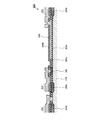
- FIG. 1 is a schematic cross-sectional view showing a configuration of a sensor described in Patent Documents 1 and 2.
- the sensor 10 includes a silicon substrate 11, a first insulating film 12 formed on one surface of the silicon substrate 11, and a second insulating film formed on the other surface of the silicon substrate 11. 13, a channel 14 disposed on the first insulating film 12, a source electrode 15 connected to one end of the channel 14, a drain electrode 16 connected to the other end of the channel 14, The reaction portion 17 is disposed on the second insulating film 13, and the gate electrode 18 is disposed so as to face the second insulating film 13.
- a recognition substance 19 such as an antibody is immobilized on the second insulating film 13.
- the gate electrode 18 is detachable, and is removed when the specimen is provided to the reaction unit 17, and is disposed so as to face the second insulating film 13 when measuring.
- the gate electrode 18 is, for example, an aluminum plate.
- the sensor described in Patent Document 1 has a channel 14 made of carbon nanotubes.
- the sensor described in Patent Document 2 has a channel 14 made of a polysilicon film.
- the silicon substrate 11, the first insulating film 12, the second insulating film 13, the channel 14, the source electrode 15, the drain electrode 16, and the gate electrode 18 function as a back gate type field effect transistor.
- a procedure for detecting a substance to be detected using the sensor 10 shown in FIG. 1 will be described.
- the voltage applied to the gate electrode 18 is swept while the gate electrode 18 is in contact with the reaction portion 17 (second insulating film 13), and the current value between the source electrode 15 and the drain electrode 16 is recorded.
- the gate electrode 18 is separated from the reaction part 17 (second insulating film 13)
- the specimen is provided to the reaction part 17, and the detection target substance contained in the specimen and the recognition immobilized on the second insulating film 13 are provided.
- the molecule 19 is reacted.
- the voltage applied to the gate electrode 18 is swept while the gate electrode 18 is again in contact with the reaction portion 17 (second insulating film 13), and the current value between the source electrode 15 and the drain electrode 16 is recorded.
- the substance to be detected can be detected from the change in the current value before and after the sample provision obtained by the above procedure.
- the conventional sensor 10 has a problem that the detection accuracy is unstable.
- the conventional sensor 10 it is necessary to remove the gate electrode 18 from the second insulating film 13 or dispose the gate electrode 18 on the second insulating film 13 a plurality of times.
- the contact state with the film 13 changes every time.
- the gate electrode 18 made of an aluminum plate or the like is placed on the second insulating film 13, defects are easily formed in the second insulating film 13. For these reasons, in the conventional sensor 10 described above, variations in the contact state of the gate electrode and charge injection into the silicon substrate due to the breakdown of the insulating film are likely to occur, resulting in unstable detection accuracy.
- An object of the present invention is to provide a sensor and a sensor module excellent in detection accuracy and stability, and a detection method using them.
- a first capacitor electrode made of a plate-like conductor or semiconductor, a first terminal electrically connected to the first capacitor electrode, which can be electrically connected to the outside, and the first capacitor electrode
- a first insulating film disposed on one surface, and a second capacitor electrode made of a conductor or a semiconductor disposed to face a part of the first capacitor electrode with the first insulating film interposed therebetween;
- a variable resistance element including a third terminal formed and a fourth terminal electrically connected to the other end of the base, and on the other surface of the first capacitor electrode directly or via a second insulating film And a reaction part disposed.
- the sensor according to [1], wherein the first capacitor electrode is a silicon substrate doped with impurities.
- the substrate is a carbon nanotube or a polysilicon film.
- the substrate is a non-doped polysilicon film.
- the first capacitor electrode is a silicon substrate doped with impurities, the base is a polysilicon film, and the third terminal and the fourth terminal are polysilicon films doped with impurities.
- the present invention also relates to the following sensor module.
- the sensor includes the variable resistance element and A sensor module fixed to the sensor module substrate such that the sensor module substrate faces the sensor module substrate.
- the sensor module according to [10] wherein two sensors are fixed to the sensor module substrate.
- the present invention also relates to the following detection method.
- a detection method comprising: a third step of providing a specimen to the reaction unit; and a fourth step of measuring a current value between the third terminal and the fourth terminal after the third step.
- a third step of providing a specimen to the reaction unit, and after the third step, the third terminal and the fourth terminal of the one sensor Current value between And a fourth step of measuring a difference value between the current value between the fourth terminal and the third terminal for the other sensors, the detection method.
- the presence or absence of the substance to be detected can be detected with high accuracy and the concentration of the substance to be detected can be measured.
- FIG. 3A to 3E are diagrams showing manufacturing steps of the sensor shown in FIG. 4A and 4B are diagrams showing an example of the configuration of the sensor module of the present invention.
- 5A and 5B are diagrams showing another example of the configuration of the sensor module of the present invention.
- 6A to 6C are cross-sectional views of the sensor of the present invention for explaining the principle of operation.
- 3 is a partial enlarged cross-sectional view of the sensor according to Embodiment 1.
- FIG. It is the elements on larger scale of the part shown with a broken line in FIG. 6 is a partial enlarged cross-sectional view of a sensor according to Embodiment 2.
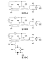
- FIG. 13A and 13B are cross-sectional views showing the configuration of the element used in Confirmation Experiments 1 to 3.
- 14A and 14B are diagrams showing two types of circuits used in the confirmation experiments 1 to 3.
- FIG. It is a graph which shows the measurement result of the confirmation experiment 1. It is a graph which shows the measurement result of the confirmation experiment 2.
- FIG. 10 is a graph showing measurement results of confirmation experiment 3.
- 18A and 18B are cross-sectional views showing the configuration of the elements used in Confirmation Experiments 4-6.
- 19A to 19C are diagrams showing three types of circuits used in the confirmation experiments 4 to 6.
- FIG. It is a graph which shows the measurement result of the confirmation experiment 4.
- 11 is a graph showing measurement results of confirmation experiment 5.
- It is a graph which shows the measurement result of the confirmation experiment 6.
- FIG. 2 is a schematic cross-sectional view showing an example of the configuration of the sensor of the present invention.
- the sensor 100 of the present invention includes a first capacitor electrode 110, a first terminal 112, a first insulating film 120, a second insulating film 130, a second capacitor electrode 140, a second terminal 142, a variable.
- a resistance element 150 and a reaction unit 160 are included.
- the first capacitor electrode 110 is a plate-like conductor or semiconductor.
- the first capacitor electrode 110 also functions as a substrate for the sensor 100.
- the first capacitor electrode 110 is a silicon substrate doped with impurities.
- Other examples of the material of the first capacitor electrode 110 include germanium, gallium arsenide (GaAs), indium phosphide (InP), zinc telluride (ZnTe), aluminum, magnesium, and the like.
- the thickness of the first capacitor electrode 110 is not particularly limited, and is, for example, about 0.5 mm.
- the first terminal 112 is electrically connected to the first capacitor electrode 110. By providing the first terminal 112, the first capacitor electrode 110 can be easily connected to an external power source.
- the position of the first terminal 112 is not particularly limited.
- the first terminal 112 is disposed on the first insulating film 120 (including the interlayer film formed thereon) (see FIGS. 5 and 7 to 9).
- the first insulating film 120 is an insulating film disposed on one surface of the first capacitor electrode 110
- the second insulating film 130 is an insulating film disposed on the other surface of the first capacitor electrode 110.
- the first insulating film 120 insulates between the first capacitor electrode 110 and the second capacitor electrode 140 and between the first capacitor electrode 110 and the variable resistance element 150.
- the first insulating film 120 may be disposed on the entire surface of one surface of the first capacitor electrode 110 or may be disposed only on a part of the first capacitor electrode 110 as long as the function can be exhibited. Further, the film thickness of the first insulating film 120 may be constant or may be different for each place.
- the second insulating film 130 insulates between the first capacitor electrode 110 and the reaction unit 160.
- the second insulating film 130 may be disposed on the entire other surface of the first capacitor electrode 110 or may be disposed on only a part of the first capacitor electrode 110 as long as the function can be exhibited.
- the film thickness of the second insulating film 130 may be constant or may vary from place to place, but in the region where the reaction unit 160 is disposed, the film thickness of the second insulating film 130 is constant. Preferably there is.
- Each of the first insulating film 120 and the second insulating film 130 may be a single layer or may be composed of two or more layers.
- the first insulating film 120 and the second insulating film 130 are, for example, silicon oxide films.
- Other examples of the material of the first insulating film 120 and the second insulating film 130 include silicon nitride, aluminum oxide, titanium oxide, acrylic resin, polyimide, and the like.
- the film thicknesses of the first insulating film 120 and the second insulating film 130 are not particularly limited.
- the second capacitor electrode 140 is a member made of a conductor or a semiconductor disposed on the first insulating film 120.
- the second capacitor electrode 140 faces the first capacitor electrode 110 with the first insulating film 120 interposed therebetween.
- the first capacitor electrode 110, the first insulating film 120, and the second capacitor electrode 140 constitute a capacitor.
- the second capacitor electrode 140 is a film made of, for example, polysilicon, metal, or alloy. Examples of the metal and alloy constituting the second capacitor electrode 140 include aluminum, an aluminum alloy, copper, a copper alloy, and the like.
- the polarity of the impurities doped into the first capacitor electrode 110 and the first The polarities of the impurities doped in the two-capacitance electrode 140 may be the same, but are preferably different from each other.
- the variable resistance element 150 is disposed on the first insulating film 120 and functions as a transducer.
- the variable resistance element 150 includes a base 152 disposed on the first insulating film 120, a third terminal 154 electrically connected to one end of the base 152, and an electrical connection to the other end of the base 152. And a fourth terminal 156 connected to the.
- a voltage is applied between the third terminal 154 and the fourth terminal 156 between the third terminal 154 and the fourth terminal 156.
- the variable resistance element 150 (base 152) has a resistance value due to the influence of isolated charges accumulated in the first capacitance electrode 110 and charges in the first capacitance electrode 110 induced by the charges generated in the reaction unit 160. Change.
- the substrate 152 is, for example, a carbon nanotube or a polysilicon film.
- the substrate 152 may be a polysilicon film doped with low-concentration impurities or a non-doped polysilicon film.
- the third terminal 154 and the fourth terminal 156 are, for example, aluminum films. Further, when the substrate 152 is a polysilicon film, the third terminal 154 and the fourth terminal 156 may be a polysilicon film doped with impurities.
- the base 152 is a polysilicon film doped with low-concentration impurities
- the third terminal 154 and the fourth terminal 156 are polysilicon films doped with impurities
- the polarity of the impurity doped into the base 152, the first The polarities of the impurities doped in the third terminal 154 and the fourth terminal 156 are preferably the same.
- the base 152 is a polysilicon film
- the third terminal 154 and the fourth terminal 156 are polysilicon films doped with impurities
- the first capacitor electrode 110 is a silicon substrate doped with impurities
- the polarity of the impurity doped in the first capacitor electrode 110 and the polarity of the impurity doped in the third terminal 154 and the fourth terminal 156 may be the same, but are preferably different from each other.
- the shape and size of the substrate 152 are not particularly limited. From the viewpoint of utilizing the shielding effect from the outside, the base 152 is preferably surrounded by the second capacitor electrode 140. Therefore, the size of the base 152 is preferably a size that can be surrounded by the second capacitor electrode 140.
- the reaction unit 160 is disposed on the second insulating film 130 and is provided with a specimen that can contain a substance to be detected.
- a recognition substance 162 that can react with the substance to be detected is immobilized on the second insulating film 130 in advance.
- the type of the recognition substance 162 is not particularly limited as long as it can react with the substance to be detected, and may be an organic substance or an inorganic substance. Examples of the recognition substance 162 include antibodies, antigens, enzymes, lectins, nucleic acids and the like.
- the sensor 100 in which the second insulating film 130 exists between the first capacitor electrode 110 and the reaction unit 160 has been described, but the second insulating film 130 may be omitted. That is, the reaction unit 160 may be directly disposed on the other surface of the first capacitance electrode 110. In this case, the recognition substance is immobilized on the other surface of the first capacitance electrode 110.
- the method for manufacturing the sensor 100 is not particularly limited.
- the sensor 100 can be manufactured by a general semiconductor element manufacturing process.
- FIG. 3 is a diagram showing an example of a manufacturing process of the sensor 100 shown in FIG.
- the description of the process of forming the first terminal 112 and the second terminal 142 is omitted.
- a first insulating film 120 and a second insulating film 130 are formed on both surfaces of the first capacitor electrode 110, respectively.
- the first capacitor electrode 110 is a silicon substrate doped with impurities
- a silicon oxide film having a desired thickness can be formed on the silicon substrate by a thermal oxidation method or a LOCOS method.
- the reaction unit 160 is directly disposed on the other surface of the first capacitor electrode 110, the second insulating film 130 may not be formed.
- variable resistance element 150 is formed at a predetermined position on the first insulating film 120.
- a rectangular polysilicon film not doped with impurities or a polysilicon film doped with low-concentration impurities (base 152) is formed at a predetermined position on the first insulating film 120 (FIG. 3B).
- the third terminal 154 and the fourth terminal 156 are formed by doping impurities into both ends of the polysilicon film (base 152) (FIG. 3C).
- the third terminal 154 and the fourth terminal 156 are formed by doping impurities at both ends of the polysilicon film (base 152) doped with low-concentration impurities, the polarity of the impurity doped into the base 152, The polarities of the impurities doped in the third terminal 154 and the fourth terminal 156 are preferably the same.
- the first capacitor electrode 110 is a silicon substrate doped with impurities, it is preferable that both ends of the polysilicon film are doped with impurities having a polarity different from that of the impurities doped in the silicon substrate.
- a third terminal 154 and a fourth terminal 156 made of metal may be connected to both ends of the polysilicon film (base 152) (see FIGS. 5 to 9).
- the second capacitor electrode 140 is formed on the first insulating film 120 at a predetermined position that does not contact the variable resistance element 150.
- a polysilicon film or an aluminum film doped with impurities is formed at a predetermined position on the first insulating film 120.
- the polysilicon film serving as the second capacitor electrode 140 includes silicon.
- the substrate is doped with an impurity having a polarity different from that of the impurity doped.
- a predetermined position on the second insulating film 130 is modified with a recognition substance 162 to form a reaction portion 160.
- the antibody is immobilized at a predetermined position on the second insulating film 130.
- the reaction unit 160 is directly disposed on the other surface of the first capacitor electrode 110, the antibody is immobilized on the other surface of the first capacitor electrode 110.
- the sensor 100 shown in FIG. 2 can be manufactured by the above procedure.
- the sensor of the present invention may further include an interlayer film or the like (see FIGS. 5 and 7 to 9).
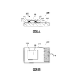
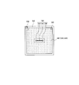
- FIG. 4 is a schematic cross-sectional view showing an example of the configuration of the sensor module of the present invention.
- 4A is a schematic cross-sectional view of the sensor module
- FIG. 4B is a schematic plan view of the sensor module.
- the sensor module 200 of the present invention includes the sensor 100 and the sensor module substrate 210 of the present invention. In FIG. 4, some components of the sensor 100 are omitted (the same applies to FIG. 5).
- the sensor module substrate 210 has a connection terminal 212 for connecting the sensor 100 and an external device (such as a power supply device or a measurement device).
- the connection terminal 212 is electrically connected to a fifth terminal 214 and a sixth terminal 216 formed on the sensor module substrate 210.
- the sensor 100 is fixed to the sensor module substrate 210 so that the variable resistance element 150 of the sensor 100 and the sensor module substrate 210 face each other. Therefore, the reaction unit 160 is always exposed to the outside (user side).
- the third terminal 154 and the fourth terminal 156 of the variable resistance element 150 are connected and fixed to the fifth terminal 214 and the sixth terminal 216 of the sensor module substrate 210, respectively.
- a conductive fixing material 220 such as solder or silver paste is used.
- an insulating adhesive may be injected between the sensor 100 and the sensor module substrate 210 and cured.
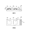
- FIG. 5 is a schematic cross-sectional view showing another example of the configuration of the sensor module of the present invention.
- the sensor module 200 ′ may include two sensors 100 a and 100 b having the same specifications and the same characteristics.
- One sensor 100a is used for detection, and the other sensor 100b is used for reference. Since the external measuring device can eliminate the influence of the external environment by using the difference value between the outputs of the two sensors 100a and 100b, it can detect the detected substance with higher accuracy and higher sensitivity.
- FIG. 6A to 6C are schematic cross-sectional views of the sensor 100 for explaining the operation principle of the sensor 100.
- the recognition substance 162 is omitted.
- the first terminal 112 and the second terminal 142 are connected to a power source (indicated by black circles in the figure), and a predetermined voltage is applied between the first capacitor electrode 110 and the second capacitor electrode 140. At this time, it is preferable to apply a voltage so that a depletion layer is not formed in a portion of the first capacitor electrode 110 on the first insulating film side and a portion of the second capacitor electrode 140 on the first insulating film side.
- the first capacitor electrode 110, the first insulating film 120, and the second capacitor electrode 140 constitute a capacitor 170. Therefore, as shown in FIG. 6A, electric charges that can be uniquely controlled by the applied voltage and the capacitance value of the capacitor 170 can be accumulated in the first insulating film 120 and the second capacitor electrode 140.
- the first terminal 112 and the second terminal 142 are disconnected from the power source (indicated by white circles in the figure), and the first capacitor electrode 110 and the second capacitor electrode 140 are set in an isolated state (not shown). Thereby, the accumulated charges in the first capacitor electrode 110 and the second capacitor electrode 140 become isolated charges. This isolated charge greatly affects the detection sensitivity of the sensor 100. Accordingly, the voltage applied between the first capacitor electrode 110 and the second capacitor electrode 140 is appropriately set according to the required detection sensitivity.
- a predetermined voltage is once applied between the third terminal 154 and the fourth terminal 156 of the variable resistance element 150 (indicated by a black circle in the figure), and the third terminal 154 and the fourth terminal 156 are connected. Measure the current value between.
- the specimen is provided to the reaction unit 160, and the target substance contained in the specimen is reacted with the recognition molecule 162 immobilized on the second insulating film 130.
- electric charges are generated on the second insulating film 130 by this reaction.
- a new charge that is polarized is induced in the first capacitor electrode 110 by the electric field generated by the charge generated on the second insulating film 130.
- the electric field generated by the charge generated by the reaction between the recognition molecule 162 directly immobilized on the other surface of the first capacitor electrode 110 and the substance to be detected contained in the specimen A charge that is polarized in the first capacitor electrode 110 is newly induced.
- a predetermined voltage (the same voltage as the first measurement) is applied again between the third terminal 154 and the fourth terminal 156 of the variable resistance element 150, and the third terminal 154 and the fourth terminal 156 are applied. Measure the current value between.
- the second measurement after the sample is provided may be performed before the sample is dried or may be performed after the sample is dried.
- the resistance value of the variable resistance element 150 is determined by the electric field formed by the isolated charges accumulated in the first capacitance electrode 110.
- the resistance value of the variable resistance element 150 is the first polarization-induced by the isolated charge accumulated in the first capacitance electrode 110 and the charge generated in the reaction unit 160. It is determined by the electric field formed by the charge in the capacitor electrode 110. Therefore, it is possible to detect the presence or absence of the substance to be detected or measure the concentration of the substance to be detected from the change in the current value before and after the sample is provided.
- the range in which the resistance value changes sharply is usually limited. For this reason, it is necessary to adjust the amount of isolated charges in the first capacitor electrode 110 so that the resistance value of the variable resistance element 150 changes sharply due to the change in the electric field caused by the reaction in the reaction unit 160. .
- the sensor 100 can be used to detect the presence or absence of the substance to be detected or to measure the concentration of the substance to be detected.
- the residual charges of the first capacitor electrode 110 and the second capacitor electrode 140 are removed immediately before the voltage is applied between the first capacitor electrode 110 and the second capacitor electrode 140. Is preferred. In this way, the amount of isolated charges in the first capacitor electrode 110 can be controlled with higher accuracy.
- the first terminal 112 and the second terminal 142 are connected to a power source at the same time, and a predetermined capacitance is provided between the first capacitance electrode 110 and the second capacitance electrode 140. Apply voltage. Thereby, in each of the two sensors 100 a and 100 b, electric charges that can be uniquely controlled by the applied voltage and the capacitance value of the capacitor 170 can be accumulated in the first insulating film 120 and the second capacitor electrode 140.
- the first terminal 112 and the second terminal 142 are simultaneously disconnected from the power source, and the first capacitor electrode 110 and the second capacitor electrode 140 are set in an isolated state. Thereby, in each of the two sensors 100a and 100b, the accumulated charges in the first capacitor electrode 110 and the second capacitor electrode 140 become isolated charges.
- the same predetermined voltage is applied between the third terminal 154 and the fourth terminal 156 of the variable resistance element 150 in each of the two sensors 100a and 100b. Then, a difference value between the current value in the detection sensor 100a and the current value in the reference sensor 100b is measured. If the difference value is not 0, offset adjustment is performed so that the difference value becomes 0 in an external measurement device.
- a sample is provided to the reaction unit 160 in the detection sensor 100a, and the detection target substance contained in the sample is reacted with the recognition molecule 162 immobilized on the reaction unit 160.
- the reference sensor 100b does not provide a sample.
- a predetermined voltage (the same voltage as the first measurement) is applied between the third terminal 154 and the fourth terminal 156 of the variable resistance element 150.
- the current value between the third terminal 154 and the fourth terminal 156 is measured.
- the resistance value of the variable resistance element 150 is determined by the electric field formed by the isolated charges accumulated in the first capacitance electrode 110.
- the resistance value of the variable resistance element 150 is the first polarization-induced by the isolated charge accumulated in the first capacitance electrode 110 and the charge generated in the reaction unit 160. It is determined by the electric field formed by the charge in the capacitor electrode 110.
- the difference between the current values of the two sensors 100a and 100b is adjusted to 0 before the sample is provided, the difference between the current values of the two sensors 100a and 100b after the sample is provided is determined by the detection sensor 100a. This value reflects only the effect of the charge generated by the reaction unit 160.
- the difference between the current values of the two sensors 100a and 100b can be amplified using an external measurement device in order to improve sensitivity. Therefore, by measuring the difference between the current values of the two sensors 100a and 100b, it is possible to detect the presence or absence of the substance to be detected or measure the concentration of the substance to be detected.
- the sensor module 200 ′ can be used to detect the presence or absence of a substance to be detected or measure the concentration of the substance to be detected with high sensitivity and high accuracy.
- the sensor 100 and the sensor modules 200 and 200 ′ according to the present invention do not need to repeatedly contact the electrodes unlike the conventional sensors (see Patent Documents 1 and 2).
- the presence or absence of the detection substance can be detected, or the concentration of the detection substance can be measured.
- the sensor 100 and the sensor modules 200 and 200 ′ of the present invention can easily and stably improve the detection sensitivity by adjusting the amount of isolated charges in the first capacitor electrode 110.
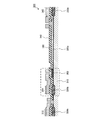
- FIG. 7 is a partially enlarged cross-sectional view of the sensor 300 according to the first embodiment.
- a part of the first capacitor electrode 310, the second insulating film, and the reaction part are omitted.
- FIG. 8 is a partially enlarged plan view of a portion indicated by a broken line in FIG. In FIG. 8, the position of the base 352 is indicated by a broken line.
- the cross-sectional view shown in FIG. 7 shows a cross section taken along line AA shown in FIG.
- the sensor 300 includes a first capacitor electrode 310, a first terminal 312, a first insulating film 320, a second insulating film (not shown), a second capacitor electrode 340, and a second terminal. 342, a base 352, a third terminal 354, a fourth terminal 356, a reaction part (not shown), and an interlayer film 380.
- the first capacitor electrode 310 is a silicon substrate doped with impurities.
- a first insulating film 320 made of silicon oxide is formed on one surface of the first capacitor electrode 310, and a second insulating film (not shown) made of silicon oxide is formed on the other surface.
- the first insulating film 320 includes a thin silicon oxide film 320a formed by a thermal oxidation method and a thick silicon oxide film 320b formed by a LOCOS method.
- a thin silicon oxide film 320 a is formed below the base 352 and the second capacitor electrode 340.
- a thick silicon oxide film 320b is formed below the first terminal 312 and the second terminal 342, the third terminal 354, and the fourth terminal 356.
- the first terminal 312 is a terminal made of aluminum for connecting the first capacitor electrode 310 and an external power source.
- the first terminal 312 is disposed on the interlayer film 380 and is electrically connected to the first capacitor electrode 310 through a contact hole provided in the interlayer film 380.
- the second capacitor electrode 340 is a polysilicon film disposed on the first insulating film 320.
- the first capacitor electrode 310, the first insulating film 320 (thin silicon oxide film 320a), and the second capacitor electrode 340 constitute a capacitor.
- the second terminal 342 is a terminal made of aluminum for connecting the second capacitor electrode 340 and an external power source.
- the second terminal 342 is disposed on the interlayer film 380 and is electrically connected to the second capacitor electrode 340 through a contact hole provided in the interlayer film 380.
- the substrate 352 is a non-doped polysilicon film disposed on the first insulating film 320 (thin silicon oxide film 320a) or a polysilicon film doped with low-concentration impurities.
- Base 352, third terminal 354, and fourth terminal 356 constitute variable resistance element 150.
- the interlayer film 380 is an insulating film formed on the first insulating film 320, the second capacitor electrode 340, and the base 352.
- the interlayer film 380 is, for example, a silicon oxide film.
- the interlayer film 380 protects the base 352, and each terminal (the first terminal 312, the second terminal 342, the third terminal 354, and the fourth terminal 356) is electrically connected only to a predetermined member. Insulate between members.
- Other examples of the material of the interlayer film 380 include silicon nitride, aluminum oxide, hafnium oxide, zirconium oxide, titanium oxide, and the like.
- the third terminal 354 is a terminal made of aluminum for connecting one end of the base 352 and an external power source.
- the fourth terminal 356 is a terminal made of aluminum for connecting the other end of the base 352 to an external power source.
- the third terminal 354 and the fourth terminal 356 are disposed on the interlayer film 380, and are electrically connected to one end and the other end of the base 352 through contact holes provided in the interlayer film 380, respectively. It is connected.
- the sensor 300 according to the first embodiment has a larger charge injection capacity per unit area than the sensors 400, 500, and 600 according to the second to fourth embodiments, the sensor 300 can be further downsized.
- the sensor 300 according to the first embodiment has a simple configuration and can be manufactured with fewer steps.
- FIG. 9 is a partially enlarged cross-sectional view of the sensor 400 according to the second embodiment.
- a part of the first capacitor electrode 310, the second insulating film, and the reaction part are omitted.
- the same components as those of the sensor 300 according to the first embodiment are denoted by the same reference numerals, and the description thereof is omitted.
- the sensor 400 includes a first capacitor electrode 310, a first terminal 312, a first insulating film 420, a second insulating film (not shown), a second capacitor electrode 340, a second terminal 342, a base body. 352, a third terminal 354, a fourth terminal (not shown), a reaction part (not shown), and an interlayer film 380.
- the first insulating film 420 includes a thin silicon oxide film 420a and a silicon oxide film 420b formed by a thermal oxidation method, and a thick silicon oxide film 420c formed by a LOCOS method.
- the thickness of the silicon oxide film 420b is larger than the thickness of the silicon oxide film 420a.
- a thin silicon oxide film 420 a is formed below the base 352.
- a silicon oxide film 420b is formed below the second capacitor electrode 340.
- a thick silicon oxide film 420 c is formed below the first terminal 312, the second terminal 342, the third terminal 354, and the fourth terminal 356.
- the first capacitor electrode 310, the first insulating film 420 (silicon oxide film 420b formed by thermal oxidation), and the second capacitor electrode 340 constitute a capacitor.
- the thickness of the first insulating film 420 (silicon oxide film 420b formed by a thermal oxidation method) in contact with the second capacitor electrode 340 is larger than that of the sensor 300 according to the first embodiment.
- the defect density of the first insulating film 420 between the first capacitor electrode 310 and the second capacitor electrode 340 can be reduced. Since the sensor 400 according to the second embodiment has a larger charge injection capacity per unit area than the sensors 500 and 600 according to the third and fourth embodiments, the sensor 400 can be further downsized. Since the sensor 400 according to the second embodiment has a simple configuration as compared with the sensors 500 and 600 according to the third and fourth embodiments, the sensor 400 can be manufactured with fewer steps.
- FIG. 10 is a partially enlarged cross-sectional view of a sensor 500 according to the third embodiment.
- a part of the first capacitor electrode 310, the second insulating film, and the reaction part are omitted.
- the same components as those of the sensor 300 of the first embodiment are denoted by the same reference numerals, and the description thereof is omitted.
- the sensor 500 includes a first capacitor electrode 310, a first terminal 312, a first insulating film 320, a second insulating film (not shown), a second capacitor electrode 540, a second terminal 342, a base body. 352, a third terminal 354, a fourth terminal (not shown), a reaction part (not shown), a first interlayer film 580a, and a second interlayer film 580b.
- the first interlayer film 580a is an insulating film formed on the first insulating film 320 and the base 352.
- the first interlayer film 580a is, for example, a silicon oxide film.
- the first interlayer film 580a reliably insulates the first capacitor electrode 310 and the second capacitor electrode 540 together with the first insulating film 320 (thin silicon oxide film 320a).
- Other examples of the material of the first interlayer film 580a include silicon nitride, aluminum oxide, hafnium oxide, zirconium oxide, titanium oxide, and the like.
- the second capacitor electrode 540 is a polysilicon film disposed on the first interlayer film 580a.
- the first capacitor electrode 310, the first insulating film 320 (thin silicon oxide film 320a), the first interlayer film 580a, and the second capacitor electrode 540 constitute a capacitor.
- the second interlayer film 580b is an insulating film formed on the second capacitor electrode 540 and the first interlayer film 580a.
- the second interlayer film 580b is, for example, a silicon oxide film.
- the second interlayer film 580b insulates each member so that each terminal (the first terminal 312, the second terminal 342, the third terminal 354, and the fourth terminal 356) is electrically connected only to a predetermined member.
- Other examples of the material of the second interlayer film 580b include silicon nitride, aluminum oxide, hafnium oxide, zirconium oxide, titanium oxide, and the like.
- the sensor 500 according to the third embodiment has a smaller charge injection capacity per unit area than the sensors 300 and 400 according to the first and second embodiments, but has high capacity reliability.
- FIG. 11 is a partially enlarged cross-sectional view of a sensor 600 according to the fourth embodiment.
- a part of the first capacitor electrode 310, the second insulating film, and the reaction part are omitted.
- the same components as those of the sensor 300 of the first embodiment are denoted by the same reference numerals, and the description thereof is omitted.
- the sensor 600 includes a first capacitor electrode 310, a first terminal 312, a first insulating film 320, a second insulating film (not shown), a second capacitor electrode 640, a second terminal 342, a base body. 352, a third terminal 354, a fourth terminal (not shown), a reaction portion (not shown), and an interlayer film 680.
- the interlayer film 680 is an insulating film formed on the first insulating film 320 and the base 352.
- the interlayer film 680 is, for example, a silicon oxide film.
- the interlayer film 680 protects the base 352, and each terminal (the first terminal 312 and the second terminal 342, the third terminal 354, the fourth terminal 356) is electrically connected only to a predetermined member. Insulate between members.
- Other examples of the material of the interlayer film 680 include silicon nitride, aluminum oxide, hafnium oxide, zirconium oxide, titanium oxide, and the like.
- the second capacitor electrode 640 is an aluminum film disposed on the interlayer film 680.
- the first capacitor electrode 310, the first insulating film 320 (thin silicon oxide film 320a), the interlayer film 680, and the second capacitor electrode 640 constitute a capacitor.
- the sensor 600 according to the fourth embodiment can be manufactured with the same number of steps as the sensor 300 according to the first embodiment, but has high capacity reliability.
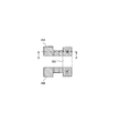
- FIG. 12 is a plan view of the sensors 300, 400, 500, and 600 in which the second capacitor electrodes 340, 540, and 640 are disposed so as to surround the variable resistance element 150.
- the interlayer film is omitted.
- a device 700 includes a silicon substrate (first capacitor electrode) 710 doped with a p-type impurity, and a silicon oxide film (first insulating film) formed on one surface of the silicon substrate 710. 720, a silicon oxide film (second insulating film) 730 formed on the other surface of the silicon substrate 710, a variable resistance element 750 disposed on the silicon oxide film 720, and a silicon oxide film 730. A back electrode 760.
- the variable resistance element 750 was manufactured by doping the n-type impurity at both ends of a non-doped polysilicon film (base) 752 having a width of 30 ⁇ m to form the third terminal 754 and the fourth terminal 756.
- a first terminal 712 for connecting to a power source for applying a voltage (V C ) for charge injection between the silicon substrate 710 and the third terminal 754 and the fourth terminal 756 is provided. Is formed.
- the third capacitor 754 and the fourth terminal 756 have the function of the second capacitor electrode without forming the second capacitor electrode. Therefore, as shown in FIG. 13B, when a charge injection voltage (V C ) is applied between the silicon substrate 710 and the third terminal 754 and the fourth terminal 756, the silicon substrate 710, the third terminal 754, and the fourth terminal A capacitor 770 is formed between the capacitor 770 and the capacitor 770.
- V C charge injection voltage
- FIG. 14 is a diagram showing two types of experimental circuits used in Confirmation Experiments 1 to 3.
- the circuit shown in FIG. 14A is a circuit for accumulating charges in a capacitor 770 formed between the silicon substrate 710 and the third terminal 754 and the fourth terminal 756.
- the circuit shown in FIG. 14B is a circuit for measuring the current I 1 between the third terminal 754 and the fourth terminal 756 after the electric charge is accumulated in the silicon substrate 710.
- the silicon substrate 710 is in an isolated state separated from the power source.
- a voltage V C is applied to a capacitor 770 formed between the silicon substrate 710 and the third terminal 754 and the fourth terminal 756, and the electric charge corresponding to the applied voltage V C in the silicon substrate 710. Was accumulated.
- a current (I 1 ) between the third terminal 754 and the fourth terminal 756 is applied with a voltage (V 1 ) of 1 V between the third terminal 754 and the fourth terminal 756.
- V 1 the applied voltage V C was repeated while changing at 1V interval from 0V to 10V.
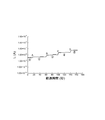
- FIG. 15 is a graph showing the measurement results. From this graph, it can be seen that the detection sensitivity of the change in the current (I 1 ) flowing through the variable resistance element 750 can be improved by appropriately selecting the applied voltage V C for accumulating charges in the silicon substrate 710. .
- FIG. 16 is a graph showing the measurement results.
- a voltage V C of ⁇ 5 V is applied to the capacitor 770 formed between the silicon substrate 710 and the third terminal 754 and the fourth terminal 756, so that the capacitor 770 is placed in the silicon substrate 710. A fixed amount of charge was accumulated.
- the voltage V 2 applied to the back electrode 760 is set to ⁇ 20V to + 20V with the voltage (V 1 ) of 1V applied between the third terminal 754 and the fourth terminal 756. Sweeping over the range, the current (I 1 ) between the third terminal 754 and the fourth terminal 756 was measured. The measurement results are shown in FIG.
- a voltage V C of 0 V is applied to a capacitor 770 formed between the silicon substrate 710 and the third terminal 754 and the fourth terminal 756, so that a predetermined amount is generated in the silicon substrate 710. The charge of accumulated.
- the voltage V 2 applied to the back electrode 760 is set to ⁇ 20V to + 20V with the voltage (V 1 ) of 1V applied between the third terminal 754 and the fourth terminal 756. Sweeping over the range, the current (I 1 ) between the third terminal 754 and the fourth terminal 756 was measured. The measurement results are shown in FIG.
- the voltage V C of + 7V to capacitance 770 formed between the silicon substrate 710 and the third terminal 754 and fourth terminal 756 is applied for 60 seconds, a predetermined amount of the silicon substrate 710 Charge was accumulated.
- a current (I 1 ) between the third terminal 754 and the fourth terminal 756 is applied with a voltage (V 1 ) of 1 V between the third terminal 754 and the fourth terminal 756.
- V 1 voltage
- FIG. 17 is a graph showing the measurement results. 17A and 17B have different numerical ranges on the vertical axis.
- A shows the timing of applying a voltage V C
- B represents a timing in which the silicon substrate 710 in an isolated state. From these graphs, it can be seen that the current (I 1 ) flowing through the variable resistance element 750, which is determined by the electric charge accumulated in the silicon substrate 710, decreases with time. This is presumably because the accumulated charges in the silicon substrate 710 leaked over time. It is considered that the small capacitance value of the capacitor 770 that accumulates the charge is weak in resistance to the leakage of the accumulated charge via the stray capacitance existing in the measurement environment.
- an element 800 includes a silicon substrate (first capacitor electrode) 810 doped with an n-type impurity, and a silicon oxide film (first insulating film) formed on one surface of the silicon substrate 810. 820, a silicon oxide film (second insulating film) 830 formed on the other surface of the silicon substrate 810, an aluminum film (second capacitor electrode) 840 disposed on the silicon oxide film 820, and a silicon oxide film 820 It has a variable resistance element 850 arranged on top and a back electrode 860 arranged on the silicon oxide film 830.
- the variable resistance element 850 was manufactured by doping the p-type impurity at both ends of a non-doped polysilicon film (base) 852 having a width of 2600 ⁇ m to form the third terminal 854 and the fourth terminal 856.
- a first terminal 812 for connecting to a power source for applying a voltage (V C ) for charge injection between the silicon substrate 810 and the aluminum film 840 is formed.
- the area of the aluminum film (second capacitor electrode) 840 is an area where an arbitrarily large capacitor can be formed as compared with the capacitor 770 in the element 700 shown in FIG. 13A.
- the aluminum film 840 also functions as a second terminal.
- Verifying Experiment 4-6 since it is the purpose of measurement of the electrical characteristics of the device 800, without forming the reaction part, provided with a rear electrode 860 for applying a desired voltage V 2 in place of the reaction unit .
- the back electrode 860 was produced by applying a silver paste on the silicon oxide film 830 and drying it.
- FIG. 19 is a diagram showing three types of experimental circuits used in confirmation experiments 4-6.
- the circuit shown in FIG. 19A is a circuit for accumulating charges in a capacitor 870 formed between the silicon substrate 810 and the aluminum film 840.
- the circuit shown in FIG. 19B is a circuit for measuring the current I 1 between the third terminal 854 and the fourth terminal 856 after accumulating charges on the silicon substrate 810.
- the silicon substrate 810 is in an isolated state separated from the power source.
- Circuit shown in FIG. 18C after charges are accumulated in the silicon substrate 810, in a state of connecting the rear electrode 860 to an external capacitor is the circuit for measuring the current I 1 between the third terminal 854 and fourth terminal 856 .
- the back surface electrode 860 is connected to an external capacitor, thereby simulating isolated charges generated by the reaction between the recognition substance and the substance to be detected in the reaction section.
- a voltage V C is applied to a capacitor 870 formed between the silicon substrate 810 and the aluminum film 840, and charges corresponding to the applied voltage V C are accumulated in the silicon substrate 810.
- a current (I 1 ) between the third terminal 854 and the fourth terminal 856 in a state where a voltage (V 1 ) of 1 V is applied between the third terminal 854 and the fourth terminal 856. was measured. The measurement of this procedure, the applied voltage V C was repeated while changing at 0.1V intervals from 0V to -4 V.
- FIG. 20 is a graph showing the measurement results. From this graph, similarly to the element 700, the detection sensitivity of the change in the current (I 1 ) flowing through the variable resistance element 850 can be improved by appropriately selecting the applied voltage V C for accumulating charges in the silicon substrate 810. It can be seen that it can be improved. Note that the directions of the characteristic curves obtained between the element 700 and the element 800 are different because of the polarity of the impurity doped in the silicon substrate 810, the polarity of the impurity doped in the third terminal 854 and the fourth terminal 856, and the application. This is because the polarity of the voltage is reversed.
- a current (I 1 ) between the third terminal 854 and the fourth terminal 856 in a state where a voltage (V 1 ) of 1 V is applied between the third terminal 854 and the fourth terminal 856. was measured over time.
- FIG. 21 is a graph showing the measurement results. 21A and 21B have different numerical ranges on the vertical axis. From these graphs, it can be seen that the current (I 1 ) flowing through the variable resistance element 850 determined by the electric charge accumulated in the silicon substrate 810 hardly changes over time. This is considered to be due to the effect of the capacitor 870 formed between the silicon substrate 810 and the aluminum film 840. From these facts, it can be seen that by forming the capacitor 870 between the silicon substrate 810 and the aluminum film 840, the influence of isolated charge leakage in the element 800 can be eliminated.
- the voltage V C of -3V to the capacity 870 which is formed between the silicon substrate 810 and the aluminum film 840 was applied for 15 seconds, a predetermined amount of charge in the silicon substrate 810 I let you.
- the current (I 1 ) between the third terminal 854 and the fourth terminal 856 was measured with the SW3 disconnected (measurement No. 1). Thereafter, the current (I 1 ) between the third terminal 854 and the fourth terminal 856 was continuously measured.
- the applied voltage V 1 between the third terminal 854 and the fourth terminal 856 was 1V.
- FIG. 22 is a graph showing the measurement results.
- “A” indicates the timing at which ⁇ 1V V 3 is applied
- “B” indicates the timing at which ⁇ 2 V V 3 is applied
- “C” indicates the timing at which ⁇ 3 V V 3 is applied
- “D” indicates the timing at which V 3 of ⁇ 4V is applied.
- the circled numbers indicate the measurement numbers. From this graph, it can be seen that the current I 1 flowing through the variable resistance element 850 changes according to the applied voltage V 3 for accumulating charges in the external capacitor C. This means that the element 800 can detect the charge generated on the back surface.
- the sensor of the present invention can detect charges generated in the reaction part on the back side.
- the sensor according to the present invention is suitable for detection of infectious diseases, confirmation of food safety, detection of environmental pollutants, and the like.
Landscapes
- Engineering & Computer Science (AREA)
- Microelectronics & Electronic Packaging (AREA)
- Power Engineering (AREA)
- Chemical & Material Sciences (AREA)
- General Physics & Mathematics (AREA)
- Physics & Mathematics (AREA)
- Computer Hardware Design (AREA)
- Condensed Matter Physics & Semiconductors (AREA)
- Health & Medical Sciences (AREA)
- Life Sciences & Earth Sciences (AREA)
- Ceramic Engineering (AREA)
- Analytical Chemistry (AREA)
- General Health & Medical Sciences (AREA)
- Biochemistry (AREA)
- Immunology (AREA)
- Pathology (AREA)
- Electrochemistry (AREA)
- Chemical Kinetics & Catalysis (AREA)
- Molecular Biology (AREA)
- Crystallography & Structural Chemistry (AREA)
- Nanotechnology (AREA)
- Investigating Or Analyzing Materials By The Use Of Electric Means (AREA)
Abstract
Description
[1]板状の導電体または半導体からなる第1容量電極と、前記第1容量電極に電気的に接続された、外部と電気的に接続されうる第1端子と、前記第1容量電極の一方の面に配置された第1絶縁膜と、前記第1絶縁膜を介して前記第1容量電極の一部と対向するように配置された、導電体または半導体からなる第2容量電極と、前記第2容量電極に電気的に接続された、外部と電気的に接続されうる第2端子と、前記第1絶縁膜上に配置された基体、前記基体の一方の端部に電気的に接続された第3端子および前記基体の他方の端部に電気的に接続された第4端子を含む可変抵抗素子と、前記第1容量電極の他方の面上に直接または第2絶縁膜を介して配置された反応部と、を有する、センサー。
[2]前記第1容量電極は、不純物をドープしたシリコン基板である、[1]に記載のセンサー。
[3]前記基体は、カーボンナノチューブまたはポリシリコン膜である、[1]または[2]に記載のセンサー。
[4]前記基体は、ノンドープポリシリコン膜である、[3]に記載のセンサー。
[5]前記第1容量電極は、不純物をドープしたシリコン基板であり、前記基体は、ポリシリコン膜であり、前記第3端子および前記第4端子は、不純物をドープしたポリシリコン膜である、[3]または[4]に記載のセンサー。
[6]前記第1容量電極にドープされた不純物の極性と前記第3端子および前記第4端子にドープされた不純物の極性とは、互いに異なる、[5]に記載のセンサー。
[7]前記第2容量電極は、ポリシリコン、金属または合金からなる膜である、[1]~[6]のいずれか一項に記載のセンサー。
[8]前記第1容量電極は、不純物をドープしたシリコン基板であり、前記第2容量電極は、不純物をドープしたポリシリコン膜であり、前記第1容量電極にドープされた不純物の極性と前記第2容量電極にドープされた不純物の極性とは、互いに異なる、[7]に記載のセンサー。
[9]前記反応部では、被検出物質と反応しうる認識物質が、前記第1容量電極の前記他方の面または前記第2絶縁膜の表面に固定化されている、[1]~[8]のいずれか一項に記載のセンサー。 The present invention relates to the following sensors.
[1] A first capacitor electrode made of a plate-like conductor or semiconductor, a first terminal electrically connected to the first capacitor electrode, which can be electrically connected to the outside, and the first capacitor electrode A first insulating film disposed on one surface, and a second capacitor electrode made of a conductor or a semiconductor disposed to face a part of the first capacitor electrode with the first insulating film interposed therebetween; A second terminal that is electrically connected to the second capacitor electrode and can be electrically connected to the outside; a base disposed on the first insulating film; and electrically connected to one end of the base A variable resistance element including a third terminal formed and a fourth terminal electrically connected to the other end of the base, and on the other surface of the first capacitor electrode directly or via a second insulating film And a reaction part disposed.
[2] The sensor according to [1], wherein the first capacitor electrode is a silicon substrate doped with impurities.
[3] The sensor according to [1] or [2], wherein the substrate is a carbon nanotube or a polysilicon film.
[4] The sensor according to [3], wherein the substrate is a non-doped polysilicon film.
[5] The first capacitor electrode is a silicon substrate doped with impurities, the base is a polysilicon film, and the third terminal and the fourth terminal are polysilicon films doped with impurities. The sensor according to [3] or [4].
[6] The sensor according to [5], wherein the polarity of the impurity doped in the first capacitor electrode and the polarity of the impurity doped in the third terminal and the fourth terminal are different from each other.
[7] The sensor according to any one of [1] to [6], wherein the second capacitor electrode is a film made of polysilicon, metal, or alloy.
[8] The first capacitor electrode is a silicon substrate doped with impurities, the second capacitor electrode is a polysilicon film doped with impurities, and the polarity of the impurities doped in the first capacitor electrode The sensor according to [7], wherein the polarities of impurities doped in the second capacitor electrode are different from each other.
[9] In the reaction section, a recognition substance that can react with a substance to be detected is immobilized on the other surface of the first capacitor electrode or the surface of the second insulating film. ] The sensor as described in any one of.
[10][1]~[9]のいずれか一項に記載のセンサーと、前記センサーと外部機器とを接続させるためのセンサーモジュール基板と、を有し、前記センサーは、前記可変抵抗素子と前記センサーモジュール基板とが対向するように、前記センサーモジュール基板に固定されている、センサーモジュール。
[11]前記センサーモジュール基板には、2つの前記センサーが固定されている、[10]に記載のセンサーモジュール。 The present invention also relates to the following sensor module.
[10] The sensor according to any one of [1] to [9], and a sensor module substrate for connecting the sensor and an external device, wherein the sensor includes the variable resistance element and A sensor module fixed to the sensor module substrate such that the sensor module substrate faces the sensor module substrate.
[11] The sensor module according to [10], wherein two sensors are fixed to the sensor module substrate.
[12][1]~[9]のいずれか一項に記載のセンサーまたは[10]に記載のセンサーモジュールを用いて検体中の被検出物質を検出する方法であって、前記第1端子および前記第2端子と電源とを電気的に接続して、前記第1容量電極と前記第2容量電極の間に電圧を印加する第1工程と、前記第1工程の後に、前記第1端子および前記第2端子を前記電源から電気的に切断して、前記第1容量電極および前記第2容量電極を前記電源から電気的に切り離した状態にする第2工程と、前記第2工程の後に、前記反応部に検体を提供する第3工程と、前記第3工程の後に、前記第3端子と前記第4端子との間の電流値を測定する第4工程と、を含む、検出方法。
[13][11]に記載のセンサーモジュールを用いて検体中の被検出物質を検出する方法であって、前記2つのセンサーの両方について同時に、前記第1端子および前記第2端子と電源とを電気的に接続して、前記第1容量電極と前記第2容量電極の間に電圧を印加する第1工程と、前記第1工程の後に、前記2つのセンサーの両方について同時に、前記第1端子および前記第2端子を前記電源から電気的に切断して、前記第1容量電極および前記第2容量電極を前記電源から電気的に切り離した状態にする第2工程と、前記第2工程の後に、前記2つのセンサーのうちの一方のセンサーにおいて、前記反応部に検体を提供する第3工程と、前記第3工程の後に、前記一方のセンサーについての前記第3端子と前記第4端子との間の電流値と、前記他方のセンサーについての前記第3端子と前記第4端子との間の電流値との差分値を測定する第4工程と、を含む、検出方法。
[14]前記第1工程の前に、前記第1容量電極および前記第2容量電極の残留電荷を除去する工程をさらに含む、[12]または[13]に記載の検出方法。 The present invention also relates to the following detection method.
[12] A method for detecting a substance to be detected in a specimen using the sensor according to any one of [1] to [9] or the sensor module according to [10], wherein the first terminal and A first step of electrically connecting the second terminal and a power source to apply a voltage between the first capacitor electrode and the second capacitor electrode; and after the first step, the first terminal and After the second step, the second step of electrically disconnecting the second terminal from the power source to electrically disconnect the first capacitor electrode and the second capacitor electrode from the power source, A detection method comprising: a third step of providing a specimen to the reaction unit; and a fourth step of measuring a current value between the third terminal and the fourth terminal after the third step.
[13] A method for detecting a substance to be detected in a sample using the sensor module according to [11], wherein the first terminal, the second terminal, and a power source are simultaneously connected to both of the two sensors. A first step of electrically connecting and applying a voltage between the first capacitor electrode and the second capacitor electrode, and after the first step, both the two sensors are simultaneously applied to the first terminal. And a second step of electrically disconnecting the second terminal from the power source to electrically disconnect the first capacitor electrode and the second capacitor electrode from the power source, and after the second step , In one of the two sensors, a third step of providing a specimen to the reaction unit, and after the third step, the third terminal and the fourth terminal of the one sensor Current value between , And a fourth step of measuring a difference value between the current value between the fourth terminal and the third terminal for the other sensors, the detection method.
[14] The detection method according to [12] or [13], further including a step of removing residual charges of the first capacitor electrode and the second capacitor electrode before the first step.
図2は、本発明のセンサーの構成の一例を示す断面模式図である。図2に示されるように、本発明のセンサー100は、第1容量電極110、第1端子112、第1絶縁膜120、第2絶縁膜130、第2容量電極140、第2端子142、可変抵抗素子150および反応部160を含む。 [Sensor configuration]
FIG. 2 is a schematic cross-sectional view showing an example of the configuration of the sensor of the present invention. As shown in FIG. 2, the
センサー100の製造方法は、特に限定されない。センサー100は、一般的な半導体素子の製造工程により製造されうる。 [Sensor manufacturing method]
The method for manufacturing the
図4は、本発明のセンサーモジュールの構成の一例を示す断面模式図である。図4Aは、センサーモジュールの断面模式図であり、図4Bは、センサーモジュールの平面模式図である。図4に示されるように、本発明のセンサーモジュール200は、本発明のセンサー100およびセンサーモジュール基板210を含む。図4では、センサー100の一部の構成要素を省略している(図5も同様)。 [Configuration of sensor module]
FIG. 4 is a schematic cross-sectional view showing an example of the configuration of the sensor module of the present invention. 4A is a schematic cross-sectional view of the sensor module, and FIG. 4B is a schematic plan view of the sensor module. As shown in FIG. 4, the
図6を参照しながら、センサー100を用いた被検出物質の検出手順の一例と、推察される検出メカニズムについて説明する。図6A~Cは、センサー100の動作原理を説明するためのセンサー100の断面模式図である。これらの図では、認識物質162が省略されている。 [How to use the sensor]
With reference to FIG. 6, an example of a detection procedure for a substance to be detected using the
次に、図5に示されるセンサーモジュール200’を用いた被検出物質の検出手順の一例について説明する。 [How to use the sensor module]
Next, an example of a procedure for detecting a substance to be detected using the
本発明のセンサーの第1絶縁膜120側の構成例について、図面を参照して詳細に説明する。以下の説明では、第2絶縁膜および反応部に関する説明を省略する。なお、各実施形態において、第2絶縁膜は無くてもよい。 [Configuration example of the first insulating film side of the sensor]
A configuration example on the first insulating
図7は、実施形態1に係るセンサー300の部分拡大断面図である。図7では、第1容量電極310の一部、第2絶縁膜および反応部を省略している。図8は、図7において破線で示される部分の部分拡大平面図である。図8では、基体352の位置を破線で示している。図7に示される断面図は、図8に示されるA-A線の断面を示している。 (Embodiment 1)
FIG. 7 is a partially enlarged cross-sectional view of the
図9は、実施形態2に係るセンサー400の部分拡大断面図である。図9では、第1容量電極310の一部、第2絶縁膜および反応部を省略している。以下の説明では、実施形態1に係るセンサー300と同一の構成要素については同一の符番を付し、その説明を省略する。 (Embodiment 2)
FIG. 9 is a partially enlarged cross-sectional view of the
図10は、実施形態3に係るセンサー500の部分拡大断面図である。図10では、第1容量電極310の一部、第2絶縁膜および反応部を省略している。以下の説明では、実施形態1のセンサー300と同一の構成要素については同一の符番を付し、その説明を省略する。 (Embodiment 3)
FIG. 10 is a partially enlarged cross-sectional view of a
図11は、実施形態4に係るセンサー600の部分拡大断面図である。図11では、第1容量電極310の一部、第2絶縁膜および反応部を省略している。以下の説明では、実施形態1のセンサー300と同一の構成要素については同一の符番を付し、その説明を省略する。 (Embodiment 4)
FIG. 11 is a partially enlarged cross-sectional view of a
2種類の素子を用いて本発明のセンサーの特性を確認した。 [Sensor characteristics]
The characteristics of the sensor of the present invention were confirmed using two types of elements.
確認実験1~3では、図13に示される素子700を用いて実験を行った。確認実験1~3では、第1容量電極と、可変抵抗素子の基体の一部を利用した第2容量電極とで構成される小さな容量でも、本発明のセンサーの機能を実現できることを確認した。 (Elements used in
In
確認実験1では、電荷注入用の印加電圧(VC)と、第3端子754-第4端子756間の電流(I1)との関係を確認した。 (Confirmation experiment 1)
In
確認実験2では、裏面電極760に印加される電圧V2と、第3端子754-第4端子756間の電流(I1)との関係を、電荷蓄積時の印加電圧Vcを変えながら繰り返し測定し、測定値の再現性を確認した。図16は、測定結果を示すグラフである。 (Verification experiment 2)
In
確認実験3では、第3端子754-第4端子756間の電流(I1)の経時変化を確認した。 (Confirmation experiment 3)
In
確認実験4~6では、図18に示される素子800を用いて実験を行った。確認実験4~6では、図13Aに示される素子700における容量770に比較して任意に大きな容量を形成することができる容量専用の第2容量電極を有する素子800を用いて、容量専用の第2容量電極を有することの効果を確認した。 (Elements used in Confirmation Experiments 4-6)
In
確認実験4では、電荷注入用の印加電圧(VC)と、第3端子854-第4端子856間の電流(I1)との関係を確認した。 (Confirmation experiment 4)
In
確認実験5では、第3端子854-第4端子856間の電流(I1)の経時変化を確認した。 (Confirmation experiment 5)
In
確認実験6では、本発明のセンサーが反応部において生成した電荷を検出できるかどうかを確認するために、素子800が裏面で生成した電荷を検出できるかどうかを確認した。 (Confirmation experiment 6)
In the
11 シリコン基板
12 第1絶縁膜
13 第2絶縁膜
14 チャネル
15 ソース電極
16 ドレイン電極
17 反応部
18 ゲート電極
19 認識物質
20 実験用素子
100,100a,100b,300,400,500,600 センサー
110,310 第1容量電極
112,312,712,812 第1端子
120,320,420 第1絶縁膜
130 第2絶縁膜
140,340,540,640,840 第2容量電極
142,342,842 第2端子
150 可変抵抗素子
152,352 基体
154,354,754,854 第3端子
156,356,756,856 第4端子
160 反応部
162 認識物質
170 容量
200,200’ センサーモジュール
210 センサーモジュール基板
212 接続端子
214 第5端子
216 第6端子
220 導電性固着材
380,680 層間膜
580a 第1層間膜
580b 第2層間膜
700,800 素子
710,810 シリコン基板
720,730,820,830 酸化シリコン膜
750,850 可変抵抗素子
752,852 ノンドープポリシリコン膜
760,860 裏面電極
770,870 シリコン基板と第2端子との間に形成される容量
840 アルミニウム膜 DESCRIPTION OF
Claims (14)
- 板状の導電体または半導体からなる第1容量電極と、
前記第1容量電極に電気的に接続された、外部と電気的に接続されうる第1端子と、
前記第1容量電極の一方の面に配置された第1絶縁膜と、
前記第1絶縁膜を介して前記第1容量電極の一部と対向するように配置された、導電体または半導体からなる第2容量電極と、
前記第2容量電極に電気的に接続された、外部と電気的に接続されうる第2端子と、
前記第1絶縁膜上に配置された基体、前記基体の一方の端部に電気的に接続された第3端子および前記基体の他方の端部に電気的に接続された第4端子を含む可変抵抗素子と、
前記第1容量電極の他方の面上に直接または第2絶縁膜を介して配置された反応部と、
を有する、センサー。 A first capacitor electrode made of a plate-like conductor or semiconductor;
A first terminal electrically connected to the first capacitor electrode and capable of being electrically connected to the outside;
A first insulating film disposed on one surface of the first capacitor electrode;
A second capacitor electrode made of a conductor or a semiconductor and disposed so as to face a part of the first capacitor electrode through the first insulating film;
A second terminal electrically connected to the second capacitor electrode and electrically connectable to the outside;
A variable including a base disposed on the first insulating film, a third terminal electrically connected to one end of the base, and a fourth terminal electrically connected to the other end of the base A resistance element;
A reaction part disposed directly or via a second insulating film on the other surface of the first capacitor electrode;
Having a sensor. - 前記第1容量電極は、不純物をドープしたシリコン基板である、請求項1に記載のセンサー。 The sensor according to claim 1, wherein the first capacitor electrode is a silicon substrate doped with impurities.
- 前記基体は、カーボンナノチューブまたはポリシリコン膜である、請求項1に記載のセンサー。 The sensor according to claim 1, wherein the substrate is a carbon nanotube or a polysilicon film.
- 前記基体は、ノンドープポリシリコン膜である、請求項3に記載のセンサー。 The sensor according to claim 3, wherein the substrate is a non-doped polysilicon film.
- 前記第1容量電極は、不純物をドープしたシリコン基板であり、
前記基体は、ポリシリコン膜であり、
前記第3端子および前記第4端子は、不純物をドープしたポリシリコン膜である、
請求項3または請求項4に記載のセンサー。 The first capacitor electrode is a silicon substrate doped with impurities;
The substrate is a polysilicon film;
The third terminal and the fourth terminal are polysilicon films doped with impurities.
The sensor according to claim 3 or claim 4. - 前記第1容量電極にドープされた不純物の極性と前記第3端子および前記第4端子にドープされた不純物の極性とは、互いに異なる、請求項5に記載のセンサー。 The sensor according to claim 5, wherein the polarity of the impurity doped in the first capacitor electrode and the polarity of the impurity doped in the third terminal and the fourth terminal are different from each other.
- 前記第2容量電極は、ポリシリコン、金属または合金からなる膜である、請求項1に記載のセンサー。 The sensor according to claim 1, wherein the second capacitor electrode is a film made of polysilicon, metal, or alloy.
- 前記第1容量電極は、不純物をドープしたシリコン基板であり、
前記第2容量電極は、不純物をドープしたポリシリコン膜であり、
前記第1容量電極にドープされた不純物の極性と前記第2容量電極にドープされた不純物の極性とは、互いに異なる、
請求項7に記載のセンサー。 The first capacitor electrode is a silicon substrate doped with impurities;
The second capacitor electrode is a polysilicon film doped with impurities,
The polarity of the impurity doped in the first capacitor electrode and the polarity of the impurity doped in the second capacitor electrode are different from each other.
The sensor according to claim 7. - 前記反応部では、被検出物質と反応しうる認識物質が、前記第1容量電極の前記他方の面または前記第2絶縁膜の表面に固定化されている、請求項1に記載のセンサー。 The sensor according to claim 1, wherein a recognition substance capable of reacting with a substance to be detected is immobilized on the other surface of the first capacitance electrode or the surface of the second insulating film in the reaction section.
- 請求項1~9のいずれか一項に記載のセンサーと、
前記センサーと外部機器とを接続させるためのセンサーモジュール基板と、を有し、
前記センサーは、前記可変抵抗素子と前記センサーモジュール基板とが対向するように、前記センサーモジュール基板に固定されている、
センサーモジュール。 A sensor according to any one of claims 1 to 9,
A sensor module substrate for connecting the sensor and an external device;
The sensor is fixed to the sensor module substrate such that the variable resistance element and the sensor module substrate face each other.
Sensor module. - 前記センサーモジュール基板には、2つの前記センサーが固定されている、請求項10に記載のセンサーモジュール。 The sensor module according to claim 10, wherein two sensors are fixed to the sensor module substrate.
- 請求項1~9のいずれか一項に記載のセンサーまたは請求項10に記載のセンサーモジュールを用いて検体中の被検出物質を検出する方法であって、
前記第1端子および前記第2端子と電源とを電気的に接続して、前記第1容量電極と前記第2容量電極の間に電圧を印加する第1工程と、
前記第1工程の後に、前記第1端子および前記第2端子を前記電源から電気的に切断して、前記第1容量電極および前記第2容量電極を前記電源から電気的に切り離した状態にする第2工程と、
前記第2工程の後に、前記反応部に検体を提供する第3工程と、
前記第3工程の後に、前記第3端子と前記第4端子との間の電流値を測定する第4工程と、
を含む、検出方法。 A method for detecting a substance to be detected in a specimen using the sensor according to any one of claims 1 to 9 or the sensor module according to claim 10,
A first step of electrically connecting the first terminal and the second terminal to a power source and applying a voltage between the first capacitor electrode and the second capacitor electrode;
After the first step, the first terminal and the second terminal are electrically disconnected from the power source, and the first capacitor electrode and the second capacitor electrode are electrically disconnected from the power source. A second step;
A third step of providing a specimen to the reaction part after the second step;
A fourth step of measuring a current value between the third terminal and the fourth terminal after the third step;
A detection method comprising: - 請求項11に記載のセンサーモジュールを用いて検体中の被検出物質を検出する方法であって、
前記2つのセンサーの両方について同時に、前記第1端子および前記第2端子と電源とを電気的に接続して、前記第1容量電極と前記第2容量電極の間に電圧を印加する第1工程と、
前記第1工程の後に、前記2つのセンサーの両方について同時に、前記第1端子および前記第2端子を前記電源から電気的に切断して、前記第1容量電極および前記第2容量電極を前記電源から電気的に切り離した状態にする第2工程と、
前記第2工程の後に、前記2つのセンサーのうちの一方のセンサーにおいて、前記反応部に検体を提供する第3工程と、
前記第3工程の後に、前記一方のセンサーについての前記第3端子と前記第4端子との間の電流値と、前記他方のセンサーについての前記第3端子と前記第4端子との間の電流値との差分値を測定する第4工程と、
を含む、検出方法。 A method for detecting a substance to be detected in a specimen using the sensor module according to claim 11,
A first step of applying a voltage between the first capacitor electrode and the second capacitor electrode by electrically connecting the first terminal and the second terminal to a power source simultaneously for both of the two sensors. When,
After the first step, simultaneously with respect to both of the two sensors, the first terminal and the second terminal are electrically disconnected from the power source, and the first capacitor electrode and the second capacitor electrode are connected to the power source. A second step of electrically separating from the second step;
After the second step, in one of the two sensors, a third step of providing a specimen to the reaction unit;
After the third step, the current value between the third terminal and the fourth terminal for the one sensor and the current between the third terminal and the fourth terminal for the other sensor A fourth step of measuring a difference value from the value;
A detection method comprising: - 前記第1工程の前に、前記第1容量電極および前記第2容量電極の残留電荷を除去する工程をさらに含む、請求項12または請求項13に記載の検出方法。 The detection method according to claim 12 or 13, further comprising a step of removing residual charges of the first capacitor electrode and the second capacitor electrode before the first step.
Priority Applications (4)
| Application Number | Priority Date | Filing Date | Title |
|---|---|---|---|
| US14/413,752 US20150192540A1 (en) | 2012-10-18 | 2013-10-17 | Sensor, sensor module, and detection method |
| JP2014541952A JP6164750B2 (en) | 2012-10-18 | 2013-10-17 | Sensor, sensor module and detection method |
| EP13847619.7A EP2910941A4 (en) | 2012-10-18 | 2013-10-17 | Sensor, sensor module, and detection method |
| US15/861,155 US20180128777A1 (en) | 2012-10-18 | 2018-01-03 | Sensor, Sensor Module, and Detection Method |
Applications Claiming Priority (2)
| Application Number | Priority Date | Filing Date | Title |
|---|---|---|---|
| JP2012-230740 | 2012-10-18 | ||
| JP2012230740 | 2012-10-18 |
Related Child Applications (2)
| Application Number | Title | Priority Date | Filing Date |
|---|---|---|---|
| US14/413,752 A-371-Of-International US20150192540A1 (en) | 2012-10-18 | 2013-10-17 | Sensor, sensor module, and detection method |
| US15/861,155 Division US20180128777A1 (en) | 2012-10-18 | 2018-01-03 | Sensor, Sensor Module, and Detection Method |
Publications (1)
| Publication Number | Publication Date |
|---|---|
| WO2014061273A1 true WO2014061273A1 (en) | 2014-04-24 |
Family
ID=50487852
Family Applications (1)
| Application Number | Title | Priority Date | Filing Date |
|---|---|---|---|
| PCT/JP2013/006170 WO2014061273A1 (en) | 2012-10-18 | 2013-10-17 | Sensor, sensor module, and detection method |
Country Status (4)
| Country | Link |
|---|---|
| US (2) | US20150192540A1 (en) |
| EP (1) | EP2910941A4 (en) |
| JP (1) | JP6164750B2 (en) |
| WO (1) | WO2014061273A1 (en) |
Cited By (2)
| Publication number | Priority date | Publication date | Assignee | Title |
|---|---|---|---|---|
| JP2015206763A (en) * | 2014-04-23 | 2015-11-19 | バイオセンサー株式会社 | Measuring device and measuring method |
| WO2017068610A1 (en) * | 2015-10-20 | 2017-04-27 | バイオセンサー株式会社 | Measuring device and measuring method |
Citations (5)
| Publication number | Priority date | Publication date | Assignee | Title |
|---|---|---|---|---|
| US20020192653A1 (en) * | 2001-06-13 | 2002-12-19 | Stetter Joseph Robert | Impedance-based chemical and biological imaging sensor apparatus and methods |
| WO2006103872A1 (en) | 2005-03-28 | 2006-10-05 | National University Corporation Hokkaido University | Carbon nano tube field effect transistor |
| JP2008507703A (en) * | 2004-07-23 | 2008-03-13 | エレクトロニック・バイオサイエンシーズ・エルエルシー | Method and apparatus for detecting a time-varying current through an ion channel |
| WO2009144878A1 (en) | 2008-05-28 | 2009-12-03 | ミツミ電機株式会社 | Sensor and method for manufacturing the same |
| US20100047901A1 (en) * | 2002-01-16 | 2010-02-25 | Nanomix, Inc. | System and method for electronic sensing of biomolecules |
Family Cites Families (7)
| Publication number | Priority date | Publication date | Assignee | Title |
|---|---|---|---|---|
| US5605612A (en) * | 1993-11-11 | 1997-02-25 | Goldstar Electron Co., Ltd. | Gas sensor and manufacturing method of the same |
| US7955559B2 (en) * | 2005-11-15 | 2011-06-07 | Nanomix, Inc. | Nanoelectronic electrochemical test device |
| CN101287986B (en) * | 2005-06-14 | 2012-01-18 | 三美电机株式会社 | Field effect transistor, biosensor provided with it, and detecting method |
| WO2007129451A1 (en) * | 2006-04-26 | 2007-11-15 | National University Corporation NARA Institute of Science and Technology | Image sensor |
| TW200914822A (en) * | 2007-05-03 | 2009-04-01 | Koninkl Philips Electronics Nv | Sensor system based on compound with solubility depending on analyte concentration |
| KR100923947B1 (en) * | 2007-12-10 | 2009-10-29 | 한국전자통신연구원 | Sensing device and sensing system |
| KR101056385B1 (en) * | 2008-10-07 | 2011-08-12 | 한국전자통신연구원 | Detection element |
-
2013
- 2013-10-17 EP EP13847619.7A patent/EP2910941A4/en not_active Withdrawn
- 2013-10-17 JP JP2014541952A patent/JP6164750B2/en active Active
- 2013-10-17 WO PCT/JP2013/006170 patent/WO2014061273A1/en active Application Filing
- 2013-10-17 US US14/413,752 patent/US20150192540A1/en not_active Abandoned
-
2018
- 2018-01-03 US US15/861,155 patent/US20180128777A1/en not_active Abandoned
Patent Citations (5)
| Publication number | Priority date | Publication date | Assignee | Title |
|---|---|---|---|---|
| US20020192653A1 (en) * | 2001-06-13 | 2002-12-19 | Stetter Joseph Robert | Impedance-based chemical and biological imaging sensor apparatus and methods |
| US20100047901A1 (en) * | 2002-01-16 | 2010-02-25 | Nanomix, Inc. | System and method for electronic sensing of biomolecules |
| JP2008507703A (en) * | 2004-07-23 | 2008-03-13 | エレクトロニック・バイオサイエンシーズ・エルエルシー | Method and apparatus for detecting a time-varying current through an ion channel |
| WO2006103872A1 (en) | 2005-03-28 | 2006-10-05 | National University Corporation Hokkaido University | Carbon nano tube field effect transistor |
| WO2009144878A1 (en) | 2008-05-28 | 2009-12-03 | ミツミ電機株式会社 | Sensor and method for manufacturing the same |
Non-Patent Citations (2)
| Title |
|---|
| MANU SEBASTIAN MANNOOR: "Nanogap Dielectric Spectroscopy for Aptamer-Based Protein Detection", BIOPHYSICAL JOURNAL, vol. 98, no. 4, February 2010 (2010-02-01), pages 724 - 732, XP055073192 * |
| See also references of EP2910941A4 |
Cited By (2)
| Publication number | Priority date | Publication date | Assignee | Title |
|---|---|---|---|---|
| JP2015206763A (en) * | 2014-04-23 | 2015-11-19 | バイオセンサー株式会社 | Measuring device and measuring method |
| WO2017068610A1 (en) * | 2015-10-20 | 2017-04-27 | バイオセンサー株式会社 | Measuring device and measuring method |
Also Published As
| Publication number | Publication date |
|---|---|
| EP2910941A1 (en) | 2015-08-26 |
| US20180128777A1 (en) | 2018-05-10 |
| EP2910941A4 (en) | 2016-05-11 |
| US20150192540A1 (en) | 2015-07-09 |
| JPWO2014061273A1 (en) | 2016-09-05 |
| JP6164750B2 (en) | 2017-07-19 |
Similar Documents
| Publication | Publication Date | Title |
|---|---|---|
| CN102375016B (en) | Backside stimulated sensor with background current manipulation | |
| US8940548B2 (en) | Sensor for biomolecules | |
| JP3053007B2 (en) | Fingerprint sensor | |
| US20140375370A1 (en) | Methods and apparatus for an isfet | |
| US10378961B2 (en) | Thermal pattern sensor | |
| US11293897B2 (en) | High sensitivity ISFET sensor | |
| US11289601B2 (en) | Negative capacitance semiconductor sensor | |
| US20220178863A1 (en) | Sensor | |
| EP3217167B1 (en) | Humidity sensors with transistor structures and piezoelectric layer | |
| US11313824B2 (en) | Detecting device | |
| JP4458135B2 (en) | Liquid property sensor | |
| TWI619941B (en) | Biosensor device | |
| JP6164750B2 (en) | Sensor, sensor module and detection method | |
| US20140295573A1 (en) | Biosensor with dual gate structure and method for detecting concentration of target protein in a protein solution | |
| US8414187B2 (en) | Pyroelectric temperature sensor and a method for measuring a temperature with the pyroelectric temperature sensor | |
| US9423375B2 (en) | Integrated circuit with nanowire sensors comprising a shielding layer, sensing apparatus, measuring method and manufacturing method | |
| JP5076364B2 (en) | Semiconductor sensor and identification method | |
| US20130057304A1 (en) | Capacitive element sensor and method for manufacturing same | |
| CN112563405A (en) | Pressure sensor unit, multi-dimensional pressure sensor and method for manufacturing the same | |
| JP2014182031A (en) | Capacitive pressure sensor and input device | |
| JP7300185B2 (en) | chemical sensor | |
| TW202211381A (en) | Integrated circuit and forming method thereof | |
| US20140212989A1 (en) | Phenytoin biosensor and method for measuring concentration of phenytoin | |
| WO2017068610A1 (en) | Measuring device and measuring method | |
| JP2014016296A (en) | Semiconductor physical quantity sensor |
Legal Events
| Date | Code | Title | Description |
|---|---|---|---|
| 121 | Ep: the epo has been informed by wipo that ep was designated in this application |
Ref document number: 13847619 Country of ref document: EP Kind code of ref document: A1 |
|
| ENP | Entry into the national phase |
Ref document number: 2014541952 Country of ref document: JP Kind code of ref document: A |
|
| WWE | Wipo information: entry into national phase |
Ref document number: 2013847619 Country of ref document: EP |
|
| WWE | Wipo information: entry into national phase |
Ref document number: 14413752 Country of ref document: US |
|
| NENP | Non-entry into the national phase |
Ref country code: DE |