WO2011045864A1 - Electronic device - Google Patents
Electronic device Download PDFInfo
- Publication number
- WO2011045864A1 WO2011045864A1 PCT/JP2009/067931 JP2009067931W WO2011045864A1 WO 2011045864 A1 WO2011045864 A1 WO 2011045864A1 JP 2009067931 W JP2009067931 W JP 2009067931W WO 2011045864 A1 WO2011045864 A1 WO 2011045864A1
- Authority
- WO
- WIPO (PCT)
- Prior art keywords
- plate
- board
- electronic device
- partial
- disposed
- Prior art date
Links
Images


Classifications
-
- G—PHYSICS
- G06—COMPUTING; CALCULATING OR COUNTING
- G06F—ELECTRIC DIGITAL DATA PROCESSING
- G06F1/00—Details not covered by groups G06F3/00 - G06F13/00 and G06F21/00
- G06F1/16—Constructional details or arrangements
- G06F1/20—Cooling means
-
- G—PHYSICS
- G06—COMPUTING; CALCULATING OR COUNTING
- G06F—ELECTRIC DIGITAL DATA PROCESSING
- G06F1/00—Details not covered by groups G06F3/00 - G06F13/00 and G06F21/00
- G06F1/16—Constructional details or arrangements
- G06F1/18—Packaging or power distribution
- G06F1/183—Internal mounting support structures, e.g. for printed circuit boards, internal connecting means
- G06F1/185—Mounting of expansion boards
-
- H—ELECTRICITY
- H05—ELECTRIC TECHNIQUES NOT OTHERWISE PROVIDED FOR
- H05K—PRINTED CIRCUITS; CASINGS OR CONSTRUCTIONAL DETAILS OF ELECTRIC APPARATUS; MANUFACTURE OF ASSEMBLAGES OF ELECTRICAL COMPONENTS
- H05K7/00—Constructional details common to different types of electric apparatus
- H05K7/20—Modifications to facilitate cooling, ventilating, or heating
- H05K7/20709—Modifications to facilitate cooling, ventilating, or heating for server racks or cabinets; for data centers, e.g. 19-inch computer racks
- H05K7/20718—Forced ventilation of a gaseous coolant
- H05K7/20727—Forced ventilation of a gaseous coolant within server blades for removing heat from heat source
Definitions
- the present invention relates to an electronic device.
- Electronic devices often achieve high-density mounting by mounting a sub board on a printed board placed in a housing. Electronic components that generate heat during operation are mounted on the printed circuit board and the sub board. If the temperature of the electronic device rises due to the heat generated by the electronic component, it causes an abnormal operation of the electronic device. For this reason, in the electronic device, it is required to cool the electronic components that generate heat.
- the riser unit U1 and the riser unit U2 are located on the same plane as the front surface S in which the respective partial plates 7 and 9 are perpendicular to the printed circuit board 12. As shown in FIG.
- the electronic components on the sub-board of the riser unit U1 are cooled by the cooling air flowing from the ventilation holes of the partial plate 9, and the electronic components on the sub-board of the riser unit U2 are It was cooled by the cooling air flowing from the vent hole 220.
- intake / exhaust holes through which cooling air for cooling electronic components passes are provided in a portion generated by moving the position of another printed circuit board forward or backward with respect to one printed circuit board.
- the intake / exhaust hole was provided in the part produced
- the cooling efficiency of the electronic components mounted on the printed circuit board is enhanced by securing more intake / exhaust holes and allowing more cooling air to flow on the printed circuit board in the housing.
- the conventional technology represented by the above-described technology has a problem that the cooling efficiency of the entire system board 20 including the electronic components on the sub-board of the riser unit is low because the intake holes are not sufficiently secured.
- the electronic components on the sub-board of the riser unit U2 were cooled by the cooling air flowing from the ventilation holes and the ventilation holes 220 of the partial plate 7.
- the electronic components on the sub-board of the riser unit U1 were cooled only by the cooling air flowing from the ventilation holes of the partial plate 9.
- the cooling efficiency of the entire system board 20 including the electronic components of the child boards of the riser unit U1 and the riser unit U2 is high. It was low.
- the disclosed technology has been made in view of the above, and in an electronic device that stores a printed circuit board on which a plurality of riser units each having a child board mounted on a riser card is stored, a sufficient amount of cooling air is ensured for printing.
- the purpose is to increase the cooling efficiency of the entire substrate.
- a housing of an electronic device includes a top plate, a bottom plate disposed to face the top plate, a first side plate, and a first side plate. It has the 2nd side plate arrange
- the housing is disposed to face the back plate and has a first partial plate having a first vent hole, and a housing that advances in parallel to the first partial plate and has a second vent hole. 2 partial plates.
- the housing is provided with a third partial plate having a third vent hole disposed in parallel with the first side plate between the top plate, the bottom plate, the first partial plate, and the second partial plate. Have.
- the electronic device includes a parent substrate disposed in a space in the housing and a first heat generating component, and is a space defined by the second partial plate and the third partial plate on the parent substrate. It is a requirement to have a first sub-board arranged on the board.
- the electronic component in an electronic device including a printed circuit board on which an electronic component is mounted in a housing, the electronic component can be efficiently and sufficiently cooled while satisfying a requirement for high-density mounting of the electronic device. There is an effect.
- FIG. 1A is a cross-sectional view of a rack of an electronic device according to an example of the first embodiment.
- FIG. 1B is a diagram showing a horizontal position of the cross-sectional view of FIG. 1A.
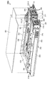
- FIG. 2A is a perspective view of the rack of the electronic device according to the example of the first embodiment as viewed from the front.
- FIG. 2B is a perspective view of the rack of the electronic device according to the example of the first embodiment as seen from the back.
- FIG. 3A is a perspective view of an IO system board according to an example of the second embodiment.
- FIG. 3B is a diagram illustrating an outline of disposing a sub board on an IO system board according to an example of the second embodiment.
- FIG. 4 is a diagram illustrating a parent board of an IO system board according to an example of the second embodiment.
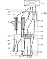
- FIG. 5A is a top view of an IO system board according to an example of the second embodiment.
- FIG. 5B is a front view of an IO system board according to an example of the second embodiment.
- FIG. 5C is a partial detailed view of an IO system board according to an example of the second embodiment.
- FIG. 6A is a diagram illustrating an inflow direction of the cooling air to the IO system board according to the example of the second embodiment.
- FIG. 6B is a diagram illustrating cable connection to an IO system board according to an example of the second embodiment.
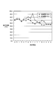
- FIG. 7 is a diagram illustrating a cooling state of an electronic component mounted on an IO system board according to an example of the second embodiment.
- FIG. 8 is a perspective view of an IO system board according to an example of the third embodiment.
- FIG. 9A is a partial detailed view of an IO system board according to an example of the third embodiment.
- FIG. 9B is a detailed top view of the sheet metal member included in the IO system board according to the example of the third embodiment.
- FIG. 9C is a detailed top view of a sheet metal member included in an IO system board according to a modification of the third embodiment.
- FIG. 10A is a top view of an IO system board according to an example of the third embodiment.
- FIG. 10B is a rear view of the IO system board according to the example of the third embodiment.
- FIG. 11A is a diagram illustrating an inflow direction of the cooling air to the system board according to the related art.
- FIG. 11B is a rear view of the system board according to the related art.
- an exemplary embodiment of an electronic device will be described in detail based on the drawings.
- the electronic apparatus will be described by taking a server apparatus in which an IO (Input Output) system board, which is a printed circuit board on which electronic components are mounted, is arranged in a casing.
- the IO system board is a connection interface through which an electronic device transmits and receives data to and from an external device.
- a child board is mounted in parallel to a parent board via a connection board called a riser card in order to improve the mounting density of electronic components in an IO system board.
- the riser card is arranged perpendicular to the parent board of the IO system board.
- the slave board is, for example, a PCI (Peripheral Component Interconnect) card that expands functions such as a network interface arranged vertically to the riser card.
- the sub board is mounted so as to be parallel to the main board.
- the casing of the electronic device is a server rack (hereinafter referred to as “rack”).
- the IO system board is a unit in which a main board, a sub board, and a riser card are arranged in a housing.
- the electronic components may include, for example, a CPU (Central Processing Unit), an MPU (Micro Processing Unit), and an MCU (Micro Control Unit).
- the electronic component may include, for example, a RAM (Random Access Memory) or a ROM (Read Only Memory).
- At least one printed circuit board on which at least one of an integrated circuit, a power supply device, which is an electronic component that generates heat, or a heat sink having fins that dissipate heat generated by the electronic component is mounted is a housing of the unit.
- the present invention can be widely applied to electronic devices arranged in the body.
- the disclosed technology can be applied to communication devices such as exchanges, routers, and LAN switches.
- the disclosed technology may be applied to a personal computer or the like on which a motherboard is mounted. That is, the disclosed technology is not limited by the following exemplary embodiment.
- FIG. 1A is a cross-sectional view of a rack of an electronic device according to an example of the first embodiment.
- FIG. 1B is a figure which shows the horizontal position of sectional drawing of FIG. 1A.
- FIG. 1B is a front view of the rack 100 of the electronic device according to the example of the first embodiment.
- the rack 100 includes a top plate 101, a bottom plate 102, a side plate 103, a side plate 104, and a shelf 111.
- the power supply device 110 is disposed on the first side plate side of the shelf 111.
- FIG. 1B shows a state in which a front plate 115, which will be described later, which is an openable / closable door disposed on the front surface of the rack 100 is released, but the front plate 115 is not shown.
- FIG. 1A is a horizontal cross-sectional view taken along the line AA of the rack 100 in FIG. 1B.
- the rack 100 may be formed of a sheet metal material. Alternatively, it may be formed of a resin material.
- the shelf 111 includes two guide panels 112-1 and 112-2 having the same number of guide rails arranged in parallel, as will be described later.
- the guide panels 112-1 and 112-2 are disposed perpendicular to the bottom plate 102 so that the horizontal positions of the bottom side, the top side, and the guide rails coincide with each other and the guide rails face each other.
- the IO system boards 200 are arranged on the plurality of guide rails facing each other, so that the plurality of IO system boards 200 are arranged in layers on the shelf 111.
- 1B is a view in which the top plate portion of the uppermost IO system board 200 in the shelf 111 is exposed.
- FIG. 1B Since a plurality of IO system boards 200 are arranged in layers on the shelf 111, in FIG. 1B, a line segment that divides the shelf 111 so that the IO system board 200 can be exposed in parallel with AA. If so, the cross-sectional view of any line segment is the same as FIG. 1A.
- the rack 100 includes a front plate 115 including an intake surface 118 having an intake hole, an exhaust surface 119 having an exhaust hole, and a back plate 105 facing the front plate 115.
- the rack 100 includes a side plate 103 disposed perpendicular to the bottom plate 102 and a second side plate facing the side plate 103.
- the front plate 115, the back plate 105, the side plate 103, and the second side plate are arranged perpendicular to the bottom plate 102 of the rack 100. That is, in the rack 100, the top plate 101, the bottom plate 102, the side plate 103, the side plate 104, the front plate 115, and the back plate 105 are arranged to form a rectangular parallelepiped.
- An IO system board 200 is disposed adjacent to the power supply device 110 inside the rack 100 surrounded by the front plate 115, the back plate 105, the side plate 103, and the second side plate. Note that the IO system board 200 is not limited to be disposed adjacent to the power supply device 110, and may be disposed in the whole or an arbitrary part of the rack 100.
- the IO system board 200 includes a top plate 201 and a bottom plate 202 arranged in parallel to the top plate 101 and the bottom plate 102 of the rack 100, and a first side plate 203 arranged perpendicular to the top plate 201 and the bottom plate 202. .
- the IO system board 200 includes a second side plate 204 that is disposed perpendicular to the top plate 201 and the bottom plate 202 and faces the first side plate 203.
- the IO system board 200 includes a back plate 205 disposed perpendicular to the top plate 201 and the bottom plate 202, and a first partial plate 207 disposed opposite to the back plate 205 and having a first vent hole 206.
- the IO system board 200 includes a second partial plate 209 having a second ventilation hole 208 disposed so as to be advanced in the direction of the front plate 115 of the rack 100 in parallel with the first partial plate 207.
- the IO system board 200 is disposed between the top plate 201 and the bottom plate 202, the first partial plate 207 and the second partial plate 209 in parallel with the first side plate 203, and the third vent hole 210.
- a third partial plate 211 having
- the IO system board 200 includes a top plate 201, a bottom plate 202, a back plate 205, a first partial plate 207, a second partial plate 209, and a third partial plate 211.
- a parent substrate 212 is disposed inside.
- the parent board 212 is called a mother board, on which electronic components that generate heat are mounted.
- the housing of the IO system board 200 may be formed of a sheet metal material. Alternatively, it may be formed of a resin material.
- the IO system board 200 includes a first heat generating component 213 inside the housing of the IO system board 200, and a first partition is defined by the second partial plate 209 and the third partial plate 211.
- a child substrate 214 is included.
- the heat generating component is an electronic component that generates heat during operation. Alternatively, it may be a heat radiating component such as a heat sink provided with a fin that radiates heat generated by the electronic component.
- the first sub board 214 is connected to a riser card (not shown) arranged perpendicular to the main board 212 so as to be parallel to the main board 212.
- the top plate 201 is partially omitted, and the bottom plate 202, the first partial plate 207, the second partial plate 209, the third partial plate 211, the parent substrate 212, and the first heat generation are shown.
- the component 213 and the first daughter board 214 are illustrated.
- the top plate 201 is disposed so as to close an opening that is partitioned by the back plate 205, the first partial plate 207, the second partial plate 209, and the third partial plate 211 and forms a surface facing the bottom plate 202.
- an exhaust surface 219 for exhausting the cooling air flowing on the parent substrate 212 and the first child substrate 214 from the exhaust surface 119 of the rack 100 to the exhaust surface 119 of the rack 100 is a back plate 205.
- a back plate 205 Are arranged on the same plane where the
- the IO system board 200 includes a first partial plate 207 having a first vent hole 206 and a second partial plate 209 having a second vent hole 208, as well as a third partial plate 209.
- the third partial plate 211 having the vent hole 210 is further provided. Therefore, the cooling air sucked in through the air intake surface 118 of the rack 100 of the electronic device more efficiently flows into the housing of the IO system board 200 and flows through the first child board 214 to the first.
- the heat generating component 213 can be cooled.
- FIG. 2A is a perspective view of a rack of an electronic device according to an example of a second embodiment as viewed from the front.
- FIG. 2B is a perspective view of the rack of the electronic device according to an example of the second embodiment as seen from the back. Note that, in the example of the second embodiment, the same reference numerals are given to the same components as those shown in the example of the first embodiment.
- FIG. 2A shows a state in which the front plate 115 which is an openable and closable door disposed on the front surface of the rack 100a according to an example of the second embodiment is released, but the illustration of the front plate 115 is omitted.
- ing. 2B does not show the back plate 105 included in the rack 100a.
- the rack 100a of the electronic device includes a top plate 101, a bottom plate 102, a side plate 103, a side plate 104, a shelf 108a, a shelf 108b, and a shelf 111.
- the bottom plate 102 is disposed so as to be parallel to the installation surface of the rack 100a. Further, the side plate 103 and the side plate 104 are arranged perpendicular to the bottom plate 102. Further, the top plate 101 is disposed so as to be perpendicular to the side plate 103 and the side plate 104.
- the rack 100a includes a front plate 115 (not shown) and a back plate 105 (not shown) arranged so as to face the front plate 115.
- the front plate 115 is an openable / closable door that is arranged so as to close a rectangular opening formed on the front surface of the rack 100a by the top plate 101, the bottom plate 102, the side plate 103, and the side plate 104.
- the back plate 105 is a member arranged so as to close a rectangular opening formed on the back surface of the rack 100a by the top plate 101, the bottom plate 102, the side plate 103, and the side plate 104.
- the rack 100 a includes a shelf 108 a and a shelf 108 b in a space defined by the side plate 103 and the side plate 104.
- a system board disposed in a blade-shaped housing is disposed on the shelf 108a and the shelf 108b.
- the shelf 108a includes a guide panel 109a1 having the same number of guide rails arranged in parallel and a guide panel 109a2 (not shown).
- the shelf 108b includes a guide panel 109b1 having the same number of guide rails arranged in parallel and a guide panel 109b2 (not shown).
- the guide panel 109a1 and the guide panel 109a2 are arranged perpendicular to the bottom plate 102 so that the bottom side of the guide panel and the horizontal position of each guide rail coincide and the guide rails face each other.
- the guide panel 109b1 and the guide panel 109b2 are arranged in the same manner as the guide panel 109a1 and the guide panel 109a2.
- the power supply device 110 and the shelf 111 are arranged side by side between the shelf 108a and the shelf 108b.
- the power supply device 110 is disposed on the side plate 103 side
- the shelf 111 is disposed on the side plate 104 side.
- the power supply device 110 controls power supply to an electronic device in which a system board on which electronic components are mounted and an IO system board 200a to be described later are arranged in the rack 100a.
- an IO system board 200a on which an electronic device transmits and receives data to and from an external device is arranged.
- the shelf 111 includes a guide panel 112-1 having the same number of guide rails arranged in parallel and a guide panel 112-2 (not shown).
- the guide panel 112-1 and the guide panel 112-2 are arranged perpendicular to the bottom plate 102 so that the bottom side of the guide panel and the horizontal position of each guide rail coincide and the guide rails face each other.
- the shelf 111 is provided with a guide panel 112-1 and a guide panel 112-2 in the rack 100a.
- a plurality of IO system boards 200a can be arranged in layers on the shelf 111 by arranging IO system boards 200a described later on a plurality of guide rails facing each other.
- connection board 114a called a backplane is disposed on the back surface of the shelf 108a.
- the connection board 114a is disposed so as to be perpendicular to the guide panel 109a1 and the guide panel 109a2.
- the connection substrate 114a is disposed on the back surface of the shelf 108a so as to close a rectangular opening formed including the guide panel 109a1 and the guide panel 109a2.
- connection board 114a electrically connects a plurality of system boards arranged on the shelf 108a.
- a plurality of system boards are electrically connected by connecting connection terminals of the system boards provided on the back surfaces of the casings of the plurality of system boards to the connection board 114a.
- connection board 114b called a backplane is disposed on the back surface of the shelf 108b.
- the connection substrate 114b is arranged to be perpendicular to the guide panel 109b1 and the guide panel 109b2.
- connection board 114b is arranged on the back surface of the shelf 108a so as to close a rectangular opening formed including the guide panel 109b1 and the guide panel 109b2. Similar to the connection board 114a, the connection board 114b electrically connects a system board arranged on the shelf 108b.
- the cooling device 116 and the connection board 117 are arranged side by side on the back surface of the shelf 111.
- the cooling device 116 cools electronic components mounted on the plurality of IO system boards 200 a arranged on the shelf 111.
- the connection board 117 is a backplane that electrically connects the parent boards 212 arranged in the housings of the plurality of IO system boards 200 a arranged on the shelf 111.
- the power supply device 110 is disposed between the connection substrate 117 and the side plate 103.
- FIG. 3A is a perspective view of an IO system board according to an example of the second embodiment.
- FIG. 3A shows a state in which the top plate 201 is removed from the IO system board 200a according to the example of the second embodiment, and the inside of the housing of the IO system board 200a is visible.
- the IO system board 200a includes a bottom plate 202, a first side plate 203 arranged perpendicular to the bottom plate 202, and a first side plate 203 arranged perpendicular to the bottom plate 202.
- An opposing second side plate 204 is included.
- the IO system board 200a includes a back plate 205 disposed perpendicular to the bottom plate 202, and a first partial plate 207 having a first air hole 206 disposed facing the back plate 205.
- the IO system board 200a has a second vent hole 208 that is arranged in parallel to the first partial plate 207 and advanced in the direction of the arrow shown in the figure with respect to the first partial plate 207.
- a second partial plate 209 is included.
- the first partial plate 207 and the second partial plate 209 are provided with ports to which cables are connected.
- the cable includes an IB (Interface Bus) cable, an IO cable, and a LAN (Local Area Network) cable.
- the IO system board 200a is a third plate having a third vent hole 210 disposed in parallel with the first side plate 203 between the bottom plate 202, the first partial plate 207, and the second partial plate 209.
- the partial plate 211 is included.
- the first side plate 203 has a fourth vent hole 220 in the vicinity of the first partial plate 207.
- the top plate 201 is attached to the IO system board 200a in accordance with the direction of the arrow shown by a broken line.
- the top plate 201 is formed of a first side plate 203, a second side plate 204, a back plate 205, a first partial plate 207, a second partial plate 209, and a third partial plate 211, and a bottom plate 202. It arrange
- a three-dimensional object formed including the I / O board is referred to as a housing of the IO system board 200a.
- a parent substrate 212 is arranged on a bottom plate 202 inside the housing of the IO system board 200a. Electronic components are mounted on the parent substrate 212.
- the parent substrate 212 has a connection terminal 212 a that is exposed to the outside of the housing from the hole of the back plate 205.
- the riser card 223 mounted with the child board is arranged as a parent so that the child board is arranged in a portion partitioned by the first partial plate 207 and the first side plate 203 inside the housing of the IO system board 200a. It is arranged so as to be perpendicular to the substrate 212. The child board is arranged perpendicular to the riser card 223 so as to be parallel to the parent board 212.
- 221 is arranged so as to be perpendicular to the parent substrate 212.
- the child board is arranged perpendicular to the riser card 221 so as to be parallel to the parent board 212.
- ports connected to the cables arranged on the first partial plate 207 and the second partial plate 209 are mounted on the sub boards mounted on the riser card 223 and the riser card 221 respectively.
- the port of the sub board is exposed at the first partial plate 207 and the second partial plate 209.
- FIG. 3B is a diagram illustrating an outline of disposing a sub board on an IO system board according to an example of the second embodiment.
- the child boards 214-1 and 214-2 are arranged perpendicular to the riser card 221 and parallel to the parent board 212.
- the child board 214-2 on which the heat generating component 213-2 is mounted is electrically connected to the riser card 221 by inserting a connection terminal into the connector 222 included in the riser card 221.
- the sub-board 214-1 on which the heat generating component 213-1 is mounted is also electrically connected to the riser card 221 by inserting a connection terminal into a connection socket (not shown) included in the riser card 221.
- Sub board 214-1 has port P2 for connecting a cable.
- the sub board 214-1 is mounted on the riser card 221 so that the port P 1 is exposed from the hole of the second partial plate 209.
- the child board 214-2 has a port P1 for connecting a cable.
- the sub board 214-2 is mounted on the riser card 221 so that the port P2 is exposed from the hole of the second partial plate 209.
- a unit formed including the riser card 221, the sub board 214-1, the sub board 214-2, and the second partial plate 209 is referred to as a riser unit Ua1.
- the child boards 226-1 and 226-2 are arranged perpendicular to the riser card 223 and parallel to the parent board 212.
- the child board 226-2 on which the heat generating component 225-2 is mounted is electrically connected to the riser card 223 by inserting a connection terminal into the connector 224 included in the riser card 223.
- the sub board 226-1 on which the heat generating component 225-1 is mounted is also electrically connected to the riser card 223 by inserting a connection terminal into a connection socket (not shown) included in the riser card 223.
- the child board 226-1 has a port P4 for connecting a cable.
- the sub-board 226-1 is mounted on the riser card 223 so that the port P3 is exposed from the hole of the first partial plate 207.
- the child board 226-2 has a port P3 for connecting a cable.
- the sub board 226-2 is mounted on the riser card 223 so that the port P4 is exposed from the hole of the first partial plate 207.
- a unit including the riser card 223, the sub board 226-1, the sub board 226-2, and the first partial plate 207 is referred to as a riser unit Ua2.
- the riser unit Ua2 is electrically connected to the parent substrate 212 by inserting a connection terminal (not shown) with the parent substrate 212 of the riser card 223 into a connector 229 disposed on the parent substrate 212.
- Connector 229 is arranged between guide pins 228-1 and guide pins 228-2 arranged on parent substrate 212.
- the riser unit Ua2 is attached to the parent board 212 in the direction of the arrow shown in FIG. 3B.
- the riser card 223 has a fastening metal fitting formed by a combination of a screw 227-1 and a screw 227-2 and a clamp band (not shown).
- a clamp band (not shown) is provided at a position corresponding to the position where the screw 227-1 and the screw 227-2 are attached on the surface of the riser card 223 on the side where the connector 224 is not disposed.
- the screw is a fastening member.
- the fastening member is not limited to a screw, and may be a resin or metal push pin having a retaining structure.
- the riser unit Ua2 is attached to the parent substrate 212.
- the riser unit Ua1 is also attached to the parent board 212 in the same manner as the riser unit Ua2.
- FIG. 4 is a diagram illustrating a parent board of an IO system board according to an example of the second embodiment.
- the parent substrate 212 is a plate-like member having notches corresponding to the mounting positions of the riser unit Ua1 and the riser unit Ua2.
- the riser unit Ua1 and the riser unit Ua2 are arranged on the main board 212 as the riser unit Ua1 moves forward in the direction of the arrow shown in the figure with respect to the riser unit Ua2.
- the parent board 212 is arranged such that the guide pins 240-1, the guide pins 240-2, and the connectors 241 to which the riser unit Ua1 is attached are arranged in accordance with the arrangement of the guide pins 228-1, the guide pins 228-2, and the connectors 229 to which the riser unit Ua2 is attached. Arranged forward from the position in the direction of the arrow shown in the figure.
- the guide pin 240-1, the guide pin 240-2, and the connector 241, and the guide pin 228-1, the guide pin 228-2, and the connector 229 are the same parts in the present embodiment, but are different parts. There may be.
- FIG. 5A is a top view of an IO system board according to an example of the second embodiment.
- the parent board 212 of the IO system board 200a according to the second embodiment is advanced by a distance of “C” shown in the figure relative to the riser unit Ua1 and the riser unit Ua1.
- a riser unit Ua2 is arranged.
- the IO system board 200 a includes a first side plate 203 having a fourth vent hole 220, a second side plate facing the first side plate 203 and perpendicular to the parent board 212. 204 is arranged.
- a fourth partial plate 230 is disposed on the IO system board 200a so as to face the third partial plate 211. Further, a fifth partial plate 236 is disposed between the fourth partial plate 230 and the second side plate 204 so as to be perpendicular to the parent substrate 212. The detailed structure of the peripheral portion D1 of the fourth partial plate 230 will be described later with reference to FIG. 5C.
- a back plate 205 is arranged on the IO system board 200a so as to be perpendicular to the parent substrate 212.
- the connection substrate 117 is disposed outside the area of the parent substrate 212.
- the cooling device 116 is arranged on the IO system board 200 a so that the intake surface is perpendicular to the parent board 212.
- the cooling device 116 is disposed so as to be separated from the parent substrate 212 by a distance of about 40 mm from the same side where the back plate 205 of the parent substrate 212 is located.
- the riser unit Ua1 has advanced by a distance of “C”, so that a rectangular mounting area 233 having the length “A” and the length “C” illustrated in FIG. 5A is generated.
- An electronic component 234 can be further arranged in the mounting area 233 on the parent substrate 212.
- An electronic component 235 is disposed on the second side plate 204 side of the electronic component 234.
- the wiring distance to the riser unit Ua1 and / or Ua2 may be shortened by mounting in the mounting area 233. it can.
- electronic components 231 (“a” to “h”) are mounted on the parent substrate 212.
- electronic components 232 (“o” to “q”) are mounted on the parent substrate 212.
- Cooling device 116 is arranged outside the area of parent substrate 212 in the vicinity of electronic component 232 (“o” to “q”).
- the ventilation hole 220 included in the first side plate 203, the ventilation hole included in the first partial plate 207, and the communication hole included in the second partial plate 209 are provided inside the housing of the IO system board 200a. Cooling air flows from the pores. Note that the cooling air from the vent hole 220 flows into the housing of the IO system board 200a through a space generated between the first side plate 220 and the side panel 112-1 of the shelf 111.
- cooling air flows into the housing of the IO system board 200a from the vent holes of the third partial plate 211 and the fourth partial plate 230. Therefore, since the cooling air flows from many air holes into the housing of the IO system board 200a, the electronic components 231, 232, 234, and 235 can be efficiently cooled.
- FIG. 5B is a front view of an IO system board according to an example of the second embodiment.
- FIG. 5B is a diagram of an IO system board 200a according to an example of the second embodiment viewed from the direction of the first partial plate 207 and the second partial plate 209.
- the first partial plate 207 includes the IO system board 200a by screwing the screws 215-1 and 215-2 into the respective screw holes of the partial plates 237-1 and 237-2.
- the partial plate 237-1 and the partial plate 237-2 are members of the housing of the IO system board 200a arranged so as to be perpendicular to the parent board 212.
- the second partial plate 209 is formed by screwing screws 216-1 and 216-2 into the respective screw holes of the partial plate 237-3 and partial plate 237-4. Fixed to the system board 200a.
- the partial plate 237-3 and the partial plate 237-4 are arranged so as to be perpendicular to the parent substrate 212 and advanced with respect to the first partial plate 207 in the same manner as the second partial plate 209. This is a member of the housing of the IO system board 200a.
- the fifth partial plate 236 is located on the opposite side of the fixing position of the first partial plate 207 with the second partial plate 209 as the center.
- the member that fixes the port P1 to the second partial plate 209 is “i”
- the member that fixes the port P2 to the second partial plate 209 is “j”
- the port P3 is the first partial plate.
- a member to be fixed to 207 is “k”
- a member to fix the port P4 to the first partial plate 207 is “l”.
- FIG. 5C is a partial detailed view of an IO system board according to an example of the second embodiment.
- FIG. 5C is a diagram illustrating details of the peripheral portion D1 of the fourth partial plate 230.
- the fourth partial plate 230 is provided with a ventilation hole 239.
- the partial plate 237-4 is arranged so as to be perpendicular to the fourth partial plate 230.
- the third partial plate 209 is fixed to the partial plate 237-4 by screwing screws 216-2 into the screw holes of the partial plate 237-4.
- FIG. 6A is a diagram illustrating an inflow direction of the cooling air to the IO system board according to the example of the second embodiment.
- the electronic components on the sub-board of the riser unit Ua1 are cooled by the cooling air flowing from the vent holes of the third partial plate 211 in addition to the vent holes of the second partial plate 209.
- the electronic components on the sub-board of the riser unit Ua2 are cooled by the cooling air flowing from the vent holes 220 of the first side plate 204 in addition to the vent holes of the first partial plate 207. Cooled by. In this way, the electronic components mounted on the respective sub-boards of the riser unit Ua1 and the riser unit Ua2 are efficiently cooled by more cooling air flowing from more vent holes.
- the electronic component mounting area 233 is formed on the parent substrate 212 due to the forward arrangement of the riser unit Ua1, it is possible to mount a larger number of electronic components on the parent substrate 212 and achieve high-density mounting.
- the space of the parent board 212 can be saved, and the size of the IO system board 200a can be reduced.
- FIG. 6B is a diagram illustrating cable connection to an IO system board according to an example of the second embodiment.
- FIG. 6B shows an example in which the cable K is connected to the port of the riser unit Ua2.
- a cable K having a large bending radius such as an IB cable is connected to a port of the riser unit Ua2 that can secure a cable space.
- the cable space refers to a space between the first partial plate 207 and the front plate 115 of the rack 100a of the electronic device.
- FIG. 7 is a diagram illustrating a cooling state of an electronic component mounted on an IO system board according to an example of the second embodiment.
- the cooling components “a to h”, “m”, “n”, and “o to q” illustrated on the horizontal axis of FIG. 7 are the “a to h” and the electronic components of the electronic component 231 shown in FIG. 5A.
- the component 234 corresponds to “m”, the electronic component 235 “n”, and the electronic component 232 “o to q”.
- cooling components “i to l” illustrated on the horizontal axis in FIG. 7 include members “i” and “j” that fix the ports P1 to P2 illustrated in FIG. 5B to the second partial plate 209, and a port P3.
- To P4 correspond to the members “k” and “l” that respectively fix the first partial plate 207.
- vent holes 210 and 239 are provided in the third partial plate 211 and the fourth partial plate 230, respectively.
- No side opening refers to a case where the third partial plate 211 and the fourth partial plate 230 are not provided with a vent hole.
- the reason why the temperature of the cooling component “l” is higher when “with side opening” than when “without side opening” is as follows. That is, if the third partial plate 211 and the fourth partial plate 230 are provided with vent holes, the total amount of cooling air flowing into the housing of the IO system board 200a increases, but the cooling component “l” is the most. This is because the air volume of the cooling air flowing into the housing from the adjacent vent hole 220 is reduced.
- the IO system board 200a includes a first partial plate 207 having a first vent hole 206 and a second partial plate 209 having a second vent hole 208, as well as a third partial plate 209.
- the third partial plate 211 having the vent hole 210 is further provided. Therefore, the cooling air sucked through the air intake surface 118 of the rack 100a flows on the child boards 214-1 to 214-4, 226-1 to 226-4, and the heat generating components 213-1 to 213-4, 225. -1 to 225-4 can be efficiently cooled. Further, the cooling air sucked through the air intake surface 118 of the rack 100 can cool the electronic components 231, 232, 234, and 235 on the parent substrate 212 more efficiently.
- FIG. 8 is a perspective view of an IO system board according to an example of the third embodiment.
- FIG. 8 shows a state where the top plate 201 is removed from the IO system board 200b according to the example of the third embodiment and the inside of the housing of the IO system board 200b is visible. Note that, in the example of the third embodiment, the same reference numerals are given to the same components as those shown in the example of the second embodiment.
- the IO system board 200b includes a sheet metal member 243-1 instead of the third partial plate 211, as compared with the IO system board 200a according to the example of the second embodiment.
- the sheet metal member 243-1 has a structure in which a sheet metal is bent so that at least two surfaces are parallel or substantially parallel. The detailed structure of the peripheral portion D2 of the sheet metal member 243-1 will be described later with reference to FIGS. 9A and 9B.
- FIG. 9A is a diagram showing details of the peripheral portion D2 of the sheet metal member 243-1.
- the sheet metal member 243-1 is provided with a ventilation hole 244.
- the second partial plate 209 is fastened through the screw 216-1 and the first partial plate 207 is fastened through the screw 215-2.
- the sheet metal member 243-1 is provided with a through hole 243a.
- a screwdriver By inserting a screwdriver into the through hole 243a in the direction of the arrow in FIG. 9A and applying the tip of the screwdriver to the screw head of the screw 215-2, the screw 215-2 can be screwed in and released. Further, the inner diameter of the through hole 243a may be taken to such an extent that a human finger can be inserted, and the screw 215-2 may be screwed in and released from the screw.
- FIG. 9B is a detailed top view of a sheet metal member included in the IO system board according to the example of the third embodiment.
- FIG. 9B is a view of the peripheral portion D2 of the sheet metal member 243-1 as viewed from the top plate 201 direction.
- the sheet metal member 243-1 includes a first surface 243-1a, a second surface 243-1b, a third surface 243-1c, a fourth surface, and the like. It has a surface 243-1d and a fifth surface 243-1e.
- the sheet metal member 243-1 has a structure in which the first surface 243-1a, the third surface 243-1c, and the fifth surface 243-1d are parallel or substantially parallel.
- the sheet metal member 243-1 has a structure in which the second surface 243-1b and the fourth surface 243-1d are parallel or substantially parallel.
- the sheet metal member 243-1 fastens the second partial plate 209 to the first surface 243-1a via the screw 216-1, and the first partial plate 207 via the screw 215-2. 5 is fastened to the surface 243-1e.
- FIG. 9C is a detailed top view of a sheet metal member included in an IO system board according to a modification of the third embodiment.
- FIG. 9C is a view of the peripheral portion of the sheet metal member 243-2 as viewed from the top plate 201 direction.
- the sheet metal member 243-2 has a first surface 243-2a, a second surface 243-2b, and a third surface 243-2c that are substantially U-shaped when viewed from the top plate 201 direction.
- the sheet metal member 243-2 has a structure in which the first surface 243-2a and the third surface 243-2c are parallel or substantially parallel.
- the sheet metal member 243-2 has a structure in which the second surface 243-1b is disposed perpendicularly or substantially perpendicular to the first surface 243-2a and the first surface 243-2c.
- the sheet metal member 243-2 fastens the second partial plate 209 to the first surface 243-2a via the screw 216-1 and also connects the first partial plate 207 via the screw 215-2 to the first partial plate 207. 3 is fastened to the surface 243-2c.
- the fastening portion of the first partial plate 207 by the screw 215-2 and the second partial plate 209 are provided.
- the fastening portion by the screw 216-1 can be overlapped.
- the arrangement interval between the riser unit Ua1 and the riser unit Ua2 can be reduced, it is possible to reduce the size of the parent board 212 and, further, the size of the housing of the IO system board 200b.
- FIG. 10A is a top view of an IO system board according to an example of the third embodiment.
- the IO system board 200b includes a sheet metal member 243-1 in place of the third partial plate 211, as compared with the IO system board 200a according to the example of the second embodiment.
- the ventilation hole 220 included in the first side plate 203, the ventilation hole included in the first partial plate 207, and the communication hole included in the second partial plate 209 are provided inside the housing of the IO system board 200b. Cooling air flows from the pores. Further, cooling air flows into the housing of the IO system board 200b from the vent holes of the sheet metal member 243-1 and the fourth partial plate 230. Therefore, the cooling air flows from many air holes into the housing of the IO system board 200b, so that the electronic components 231 and 232 can be efficiently cooled.
- the parent substrate 212 can be downsized and electronic components can be mounted on the parent substrate 212 at a high density. it can.
- FIG. 10B is a front view of an IO system board according to an example of the third embodiment.
- FIG. 10B is a diagram of an IO system board 200b according to an example of the third embodiment viewed from the direction of the first partial plate 207 and the second partial plate 209.
- the first partial plate 207 includes the IO system board 200b by screwing the screws 215-1 and 215-2 into the respective screw holes of the partial plate 237-1 and the sheet metal member 243-1. Fixed to. Partial plate 237-1 and sheet metal member 243-1 are arranged to be perpendicular to parent substrate 212.
- the second partial plate 209 is formed by screwing screws 216-1 and 216-2 into the respective screw holes of the sheet metal member 243-1 and partial plate 237-4. It is fixed to the system board 200b.
- FIG. 11A is a diagram illustrating an inflow direction of the cooling air to the system board according to the related art.
- FIG. 11B is a front view of a system board according to the prior art. As shown in FIGS. 11A and 11B, in the system board 20 according to the prior art, the riser unit U1 and the riser unit U2 are flush with the front surface S in which the respective partial plates 7 and 9 are perpendicular to the parent substrate 12. Located in.
- the electronic components on the sub-board of the riser unit U1 are cooled by the cooling air flowing from the ventilation holes of the partial plate 9. Further, the electronic components on the sub-board of the riser unit U2 are cooled by the cooling air flowing from the ventilation holes and the ventilation holes 22 of the partial plate 7.
- the cooling performance is low because the amount of cooling air that cools the electronic components of the child boards of the riser unit U1 and the riser unit U2 is insufficient.
- the disclosed technology has been made to overcome this problem.
Abstract
Description
図1Aは、第1の実施の形態の一例にかかる電子装置のラックの断面図である。また、図1Bは、図1Aの断面図の水平位置を示す図である。なお、図1Bは、第1の実施の形態の一例にかかる電子装置のラック100の前面図である。 [Example of first embodiment]
FIG. 1A is a cross-sectional view of a rack of an electronic device according to an example of the first embodiment. Moreover, FIG. 1B is a figure which shows the horizontal position of sectional drawing of FIG. 1A. FIG. 1B is a front view of the
図1Bにおいて、ラック100は、天板101、底板102、側面板103、側面板104、棚111を有する。なお、棚111の第1の側面板側には、電源装置110が配置される。図1Bは、ラック100の前面に配置される開閉可能な扉体である後述する前面板115を解放した状態を示すが、前面板115の図示を省略している。図1Aは、図1Bにおけるラック100のA-Aの水平方向の断面図である。ラック100は、板金素材で形成されてもよい。または、樹脂素材で形成されてもよい。 (Configuration of rack according to an example of the first embodiment)
1B, the
前面板115、背面板105、側面板103および第2の側面板で囲まれたラック100の内部には、電源装置110に隣接してIOシステムボード200が配置される。なお、IOシステムボード200は、電源装置110に隣接して配置されることに限定されず、ラック100の内部の全部又は任意の一部に配置してもよい。 (IO system board according to an example of the first embodiment)
An
第1の実施の形態にかかるIOシステムボード200は、第1の通気孔206を有する第1の部分板207、および、第2の通気孔208を有する第2の部分板209に加え、第3の通気孔210を有する第3の部分板211をさらに有する。よって、電子装置のラック100の吸気面118を介して吸気された冷却風がより多く効率的にIOシステムボード200の筐体内部に流入し、第1の子基板214上を流通して第1の発熱部品213を冷却することが可能になる。 (Effect of an example of the first embodiment)
The
(第2の実施の形態の一例にかかる電子装置のラックの構成)
図2Aは、第2の実施の形態の一例にかかる電子装置のラックを前面からみた斜視図である。また、図2Bは、第2の実施の形態の一例にかかる電子装置のラックを背面からみた斜視図である。なお、第2の実施の形態の一例において、第1の実施の形態の一例で示した構成と同一の構成には同一の符号を付与している。 [Example of Second Embodiment]
(Configuration of rack of electronic device according to an example of the second embodiment)
FIG. 2A is a perspective view of a rack of an electronic device according to an example of a second embodiment as viewed from the front. FIG. 2B is a perspective view of the rack of the electronic device according to an example of the second embodiment as seen from the back. Note that, in the example of the second embodiment, the same reference numerals are given to the same components as those shown in the example of the first embodiment.
先ず、図2Aを参照する。ラック100aは、側面板103および側面板104によって区画された空間内に棚108aおよび棚108bを有する。棚108aおよび棚108bには、ブレード状の筐体内に配置されたシステムボードが配置される。 (Front perspective view of a rack of an electronic device according to an example of the second embodiment)
First, refer to FIG. 2A. The
次に、図2Bを参照する。ラック100aにおいて、棚108aの背面には、バックプレーンと呼ばれる接続基板114aが配置される。接続基板114aは、ガイドパネル109a1およびガイドパネル109a2に対して垂直になるように配置される。また、接続基板114aは、棚108aの背面において、ガイドパネル109a1およびガイドパネル109a2を含んで形成される矩形の開口部を塞ぐように配置される。 (Rear perspective view of a rack of an electronic device according to an example of the second embodiment)
Reference is now made to FIG. In the
図3Aは、第2の実施の形態の一例にかかるIOシステムボードの斜視図である。図3Aは、第2の実施の形態の一例にかかるIOシステムボード200aから天板201を取り外して、IOシステムボード200aの筐体内部が可視である状態を示す。 (IO system board according to an example of the second embodiment)
FIG. 3A is a perspective view of an IO system board according to an example of the second embodiment. FIG. 3A shows a state in which the
図3Bは、第2の実施の形態の一例にかかるIOシステムボードへ子基板を配置する概要を示す図である。親基板212に対して垂直に配置されるライザーカード221には、子基板214-1および214-2が、ライザーカード221に対して垂直、かつ、親基板212に対して平行に配置される。 (Arrangement of Sub-board on IO System Board According to Example of Second Embodiment)
FIG. 3B is a diagram illustrating an outline of disposing a sub board on an IO system board according to an example of the second embodiment. In the
図4は、第2の実施の形態の一例にかかるIOシステムボードの親基板を示す図である。図4に示すように、親基板212は、ライザーユニットUa1およびライザーユニットUa2の取り付け位置に応じた切り欠きを有する板状の部材である。 (Parent board of an IO system board according to an example of the second embodiment)
FIG. 4 is a diagram illustrating a parent board of an IO system board according to an example of the second embodiment. As shown in FIG. 4, the
図5Aは、第2の実施の形態の一例にかかるIOシステムボードの上面図である。図5Aに示すように、第2の実施の形態の一例にかかるIOシステムボード200aの親基板212には、ライザーユニットUa1、および、ライザーユニットUa1に対して図示の「C」の距離だけ前進したライザーユニットUa2が配置される。 (Top view of an IO system board according to an example of the second embodiment)
FIG. 5A is a top view of an IO system board according to an example of the second embodiment. As shown in FIG. 5A, the
図5Bは、第2の実施の形態の一例にかかるIOシステムボードの前面図である。図5Bは、第2の実施の形態の一例にかかるIOシステムボード200aを第1の部分板207および第2の部分板209方向から見た図である。 (Front view of an IO system board according to an example of the second embodiment)
FIG. 5B is a front view of an IO system board according to an example of the second embodiment. FIG. 5B is a diagram of an
図5Cは、第2の実施の形態の一例にかかるIOシステムボードの部分詳細図である。図5Cは、第4の部分板230の周辺部分D1の詳細を示す図である。図5Cに示すように、第4の部分板230には、通風孔239が設けられる。また、第4の部分板230に垂直になるように部分板237-4が配置される。第3の部分板209は、ネジ216―2を部分板237-4のネジ穴に螺入することによって部分板237-4に固定される。 (Details of the peripheral portion D1 of the fourth partial plate 230)
FIG. 5C is a partial detailed view of an IO system board according to an example of the second embodiment. FIG. 5C is a diagram illustrating details of the peripheral portion D1 of the fourth
図6Aは、第2の実施の形態の一例にかかるIOシステムボードへの冷却風の流入方向を示す図である。図6Aに示すように、ライザーユニットUa1の子基板上の電子部品は、第2の部分板209が有する通気孔に加え、第3の部分板211が有する通気孔から流入する冷却風によって冷却される。 (Inflow direction of cooling air to the IO system board according to an example of the second embodiment)
FIG. 6A is a diagram illustrating an inflow direction of the cooling air to the IO system board according to the example of the second embodiment. As shown in FIG. 6A, the electronic components on the sub-board of the riser unit Ua1 are cooled by the cooling air flowing from the vent holes of the third
図6Bは、第2の実施の形態の一例にかかるIOシステムボードへのケーブル接続を示す図である。図6Bは、ライザーユニットUa2が有するポートにケーブルKを接続した例を示す。 (Cable connection to an IO system board according to an example of the second embodiment)
FIG. 6B is a diagram illustrating cable connection to an IO system board according to an example of the second embodiment. FIG. 6B shows an example in which the cable K is connected to the port of the riser unit Ua2.
図7は、第2の実施の形態の一例にかかるIOシステムボードに実装された電子部品の冷却状況を示す図である。ここで、図7の横軸に図示する冷却部品「a~h」、「m」、「n」、「o~q」は、図5Aに示した電子部品231の「a~h」、電子部品234である「m」、電子部品235である「n」、電子部品232の「o~q」にそれぞれ相当する。 (Cooling status of electronic components of an IO system board according to an example of the second embodiment)
FIG. 7 is a diagram illustrating a cooling state of an electronic component mounted on an IO system board according to an example of the second embodiment. Here, the cooling components “a to h”, “m”, “n”, and “o to q” illustrated on the horizontal axis of FIG. 7 are the “a to h” and the electronic components of the
第2の実施の形態にかかるIOシステムボード200aは、第1の通気孔206を有する第1の部分板207、および、第2の通気孔208を有する第2の部分板209に加え、第3の通気孔210を有する第3の部分板211をさらに有する。よって、ラック100aの吸気面118を介して吸気された冷却風が子基板214-1~214-4、226-1~226-4上を流通して発熱部品213-1~213-4、225-1~225-4を効率的に冷却することが可能になる。また、ラック100の吸気面118を介して吸気された冷却風が、親基板212上の電子部品231、232、234、235をさらに効率的に冷却することができる。 (Effect of an example of the second embodiment)
The
(第3の実施の形態の一例にかかるIOシステムボード)
図8は、第3の実施の形態の一例にかかるIOシステムボードの斜視図である。図8は、第3の実施の形態の一例にかかるIOシステムボード200bから天板201を取り外して、IOシステムボード200bの筐体内部が可視である状態を示す。なお、第3の実施の形態の一例おいて、第2の実施の形態の一例で示した構成と同一の構成には同一の符号を付与している。 [Example of Third Embodiment]
(IO system board according to an example of the third embodiment)
FIG. 8 is a perspective view of an IO system board according to an example of the third embodiment. FIG. 8 shows a state where the
図9A~図9Bは、第3の実施の形態の一例にかかるIOシステムボードの部分詳細図である。図9Aは、板金部材243-1の周辺部分D2の詳細を示す図である。図9Aに示すように、板金部材243-1には、通風孔244が設けられる。板金部材243-1は、ネジ216-1を介して、第2の部分板209が締結されるとともに、ネジ215-2を介して、第1の部分板207が締結される。 (Details of the peripheral portion D2 of the sheet metal member 243-1)
9A to 9B are partial detailed views of an IO system board according to an example of the third embodiment. FIG. 9A is a diagram showing details of the peripheral portion D2 of the sheet metal member 243-1. As shown in FIG. 9A, the sheet metal member 243-1 is provided with a
なお、第3の実施の形態の一例では、板金部材243-1に代えて、板金部材243-2を採用してもよい。図9Cは、第3の実施の形態の変形例にかかるIOシステムボードが有する板金部材の上面詳細図である。図9Cは、板金部材243-2の周辺部分を天板201方向から見た図である。 (Modification of sheet metal member)
In the example of the third embodiment, a sheet metal member 243-2 may be employed instead of the sheet metal member 243-1. FIG. 9C is a detailed top view of a sheet metal member included in an IO system board according to a modification of the third embodiment. FIG. 9C is a view of the peripheral portion of the sheet metal member 243-2 as viewed from the
図10Aは、第3の実施の形態の一例にかかるIOシステムボードの上面図である。図10Aに示すように、IOシステムボード200bは、第2の実施の形態の一例にかかるIOシステムボード200aと比較して、第3の部分板211に代えて、板金部材243-1を有する。 (Top view of an IO system board according to an example of the third embodiment)
FIG. 10A is a top view of an IO system board according to an example of the third embodiment. As illustrated in FIG. 10A, the
図10Bは、第3の実施の形態の一例にかかるIOシステムボードの前面図である。図10Bは、第3の実施の形態の一例にかかるIOシステムボード200bを第1の部分板207および第2の部分板209方向から見た図である。 (Front view of an IO system board according to an example of the third embodiment)
FIG. 10B is a front view of an IO system board according to an example of the third embodiment. FIG. 10B is a diagram of an
第3の実施の形態の一例では、第2の実施の形態の一例における第3の部分板211に代えて板金部材243-1を採用する。よって、第1の部分板207のネジ215-2による締結部分、および、第2の部分板209のネジ216-1による締結部分をオーバーラップさせることができる。この結果、ライザーユニットUa1およびライザーユニットUa2の配置間隔である図示の「C」を縮小することができる。よって、親基板212の小型化、親基板212への電子部品の高密度実装、延いては、IOシステムボード200bの筐体の小型化を図ることができる。 (Effect of an example of the third embodiment)
In the example of the third embodiment, a sheet metal member 243-1 is employed instead of the third
図11Aは、従来技術にかかるシステムボードへの冷却風の流入方向を示す図である。図11Bは、従来技術にかかるシステムボードの前面図である。図11Aおよび図11Bに示すように、従来技術にかかるシステムボード20において、ライザーユニットU1およびライザーユニットU2は、それぞれの部分板7および部分板9が親基板12に垂直な前面Sと同一面上に位置する。 (Direction of cooling air flow into the IO system board according to the prior art)
FIG. 11A is a diagram illustrating an inflow direction of the cooling air to the system board according to the related art. FIG. 11B is a front view of a system board according to the prior art. As shown in FIGS. 11A and 11B, in the
12 プリント基板
20 システムボード
100、100a ラック
101 天板
102 底板
103 第1の側面板
104 第2の側面板
105 背面板
108a、108b 棚
109a1、109a2、109b1、109b2 ガイドパネル
110 電源装置
111 棚
112-1、112-2 ガイドパネル
114a、114b 接続基板
115 前面板
116 冷却装置
117 接続基板
118 吸気面
119 排気面
200、200a、200b IOシステムボード
201 天板
202 底板
203 第1の側面板
204 第2の側面板
205 背面板
206 第1の通気孔
207 第1の部分板
208 第2の通気孔
209 第2の部分板
210 第3の通気孔
211 第3の部分板
212 親基板
212a 接続端子
213 第1の発熱部品
214-1、214-2 子基板
215-1、215-2、216-1、216-2 ネジ
219 排気面
220 第4の通気孔
221 ライザーカード
221 第3の部分板
222、224 コネクタ
223 ライザーカード
225-1、225-2、225-3、225-4 発熱部品
226-1、226-2 子基板
227-1、227-2 ネジ
228-1、228-2 ガイドピン
229、241 コネクタ
230 第4の部分板
231、232、234、235 電子部品
233 実装エリア
236 第5の部分板
237-1、237-2、237-3、237-4 部分板
239 通風孔
240-1、240-2 ガイドピン
243-1、243-2 板金部材
243-1a 第1の面
243-1b 第2の面
243-1c 第3の面
243-1d 第4の面
243-1e 第5の面
244 通風孔
K ケーブル
P1、P2、P3、P4 ポート
S 前面
U1、U2、Ua1、Ua2ライザーユニット 7, 9 Partial plate 12 Printed circuit board 20 System board 100, 100a Rack 101 Top plate 102 Bottom plate 103 First side plate 104 Second side plate 105 Back plate 108a, 108b Shelf 109a1, 109a2, 109b1, 109b2 Guide panel 110 Power supply Device 111 Shelf 112-1, 112-2 Guide panel 114a, 114b Connection board 115 Front plate 116 Cooling device 117 Connection board 118 Air intake surface 119 Exhaust surface 200, 200a, 200b IO system board 201 Top plate 202 Bottom plate 203 First side Face plate 204 Second side plate 205 Back plate 206 First vent hole 207 First partial plate 208 Second vent hole 209 Second partial plate 210 Third vent hole 211 Third partial plate 212 Parent substrate 212a Connection terminal 213 First heat generating component 214-1, 2 4-2 Sub-board 215-1, 215-2, 216-1, 216-2 Screw 219 Exhaust surface 220 Fourth vent hole 221 Riser card 221 Third partial plate 222, 224 Connector 223 Riser card 225-1, 225-2, 225-3, 225-4 Heat-generating component 226-1, 226-2 Sub-board 227-1, 227-2 Screw 228-1, 228-2 Guide pin 229, 241 Connector 230 Fourth partial plate 231 232, 234, 235 Electronic component 233 Mounting area 236 Fifth partial plate 237-1, 236-2, 237-3, 237-4 Partial plate 239 Ventilation holes 240-1, 240-2 Guide pins 243-1, 243-2 Sheet metal member 243-1a First surface 243-1b Second surface 243-1c Third surface 243-1d Fourth surface 243-1e 244 ventilation holes K cable P1, P2, P3, P4 port S front U1, U2, Ua1, Ua2 riser unit
Claims (9)
- 天板と、前記天板に対向して配置された底板と、第1の側面板と、前記第1の側面板に対向して配置された第2の側面板と、背面板と、前記背面板と対向して配置され第1の通気孔を有する第1の部分板と、前記第1の部分板に対し平行に前進して配置され第2の通気孔を有する第2の部分板と、前記天板と前記底板と前記第1の部分板と前記第2の部分板との間に前記第1の側面板と平行に配置され第3の通気孔を有する第3の部分板を有する筐体と、
前記筐体内の空間に配置される親基板と、
第1の発熱部品を有するとともに、前記親基板上の前記第2の部分板と前記第3の部分板で区画される空間に配置された第1の子基板を有することを特徴とする電子装置。 A top plate, a bottom plate disposed to face the top plate, a first side plate, a second side plate disposed to face the first side plate, a back plate, and the back plate A first partial plate disposed opposite to the face plate and having a first vent hole; a second partial plate disposed in advance parallel to the first partial plate and having a second vent hole; A housing having a third partial plate having a third ventilation hole disposed in parallel with the first side plate between the top plate, the bottom plate, the first partial plate, and the second partial plate. Body,
A parent substrate disposed in a space in the housing;
An electronic device comprising a first sub-board disposed in a space defined by the second partial plate and the third partial plate on the parent substrate, and having a first heat generating component . - 前記電子装置はさらに、
前記親基板上に配置された第1のコネクタと、
前記第1のコネクタに接続することにより前記親基板に対して垂直に配置されるとともに、第2のコネクタを備える第1の接続基板を有し、
前記第1の子基板は、前記第2のコネクタに接続することにより前記親基板に対向して配置されることを特徴とする請求項1記載の電子装置。 The electronic device further includes
A first connector disposed on the parent substrate;
A first connection board that is arranged perpendicular to the parent board by connecting to the first connector and includes a second connector;
The electronic device according to claim 1, wherein the first sub board is disposed to face the parent board by connecting to the second connector. - 前記電子装置はさらに、
第2の発熱部品を有するとともに、前記親基板上の前記第1の側面板と前記第1の部分板で区画される空間内に配置された第2の子基板を有することを特徴とする請求項1記載の電子装置。 The electronic device further includes
And a second sub-board disposed in a space defined by the first side plate and the first partial plate on the parent board. Item 2. The electronic device according to Item 1. - 前記電子装置はさらに、
前記親基板上に配置された第3のコネクタと、
前記第3のコネクタに接続することにより前記親基板に対して垂直に配置されるとともに、第4のコネクタを備える第2の接続基板を有し、
前記第2の子基板は、前記第4のコネクタに接続することにより前記親基板に対向して配置されることを特徴とする請求項3記載の電子装置。 The electronic device further includes
A third connector disposed on the parent substrate;
A second connection board that is arranged perpendicular to the parent board by connecting to the third connector and that includes a fourth connector;
4. The electronic device according to claim 3, wherein the second sub-board is disposed to face the parent board by connecting to the fourth connector. - 前記電子装置において、
前記第1の子基板の前縁部が前記第2の子基板の前縁部に対して前進する距離は、前記第2の部分板が前記第1の部分板に対して前進した距離以下であることを特徴とする請求項3又は4記載の電子装置。 In the electronic device,
The distance that the front edge of the first sub board advances with respect to the front edge of the second sub board is equal to or less than the distance that the second partial plate advances with respect to the first partial plate. The electronic device according to claim 3, wherein the electronic device is provided. - 前記電子装置において、
前記親基板は、
前記第1の子基板が、前記前進したことにより生じた空間に、第3の発熱部品が配置されることを特徴とする請求項5記載の電子装置。 In the electronic device,
The parent substrate is
The electronic device according to claim 5, wherein a third heat generating component is disposed in a space generated by the advancement of the first sub board. - 前記電子装置はさらに、
冷却装置を有し、
前記第1の側面板は、第4の通気孔を有し、
前記第1の子基板は、前記第2及び第3の通気孔を介して前記冷却装置により冷却され、
前記第2の子基板は、前記第1及び第4の通気孔を介して前記冷却装置により冷却されることを特徴とする請求項6記載の電子装置。 The electronic device further includes
Have a cooling device,
The first side plate has a fourth ventilation hole,
The first sub board is cooled by the cooling device through the second and third vent holes,
The electronic device according to claim 6, wherein the second sub board is cooled by the cooling device through the first and fourth vent holes. - 前記電子装置はさらに、
天板方向から見た場合に略己の字を構成する第1乃至第5の面のうち、第1の面と第3の面と第5の面が略平行且つ第2の面と第4の面が略平行に曲折する板金部材を有し、
前記板金部材は、
第1の締結部材を介して、前記第2の部分板を前記第1の面に締結するとともに、第2の締結部材を介して、前記第1の部分板を前記第5の面に締結することを特徴とする請求項4記載の電子装置。 The electronic device further includes
Of the first to fifth surfaces constituting a substantially self-shape when viewed from the top plate direction, the first surface, the third surface, and the fifth surface are substantially parallel, and the second surface and the fourth surface. A sheet metal member whose surface is bent substantially in parallel,
The sheet metal member is
The second partial plate is fastened to the first surface via a first fastening member, and the first partial plate is fastened to the fifth surface via a second fastening member. The electronic device according to claim 4. - 前記電子装置はさらに、
天板方向から見た場合に略コの字を構成する第1乃至第3の面のうち、第1の面と第3の面が略平行且つ第2の面が前記第1の面と前記第3の面に対して垂直に曲折する板金部材を有し、
前記板金部材は、
第1の締結部材を介して、前記第2の部分板を前記第1の面に締結するとともに、第2の締結部材を介して、前記第1の部分板を前記第3の面に締結することを特徴とする請求項4記載の電子装置。 The electronic device further includes
Of the first to third surfaces constituting a substantially U shape when viewed from the top plate direction, the first surface and the third surface are substantially parallel, and the second surface is the first surface and the A sheet metal member that bends perpendicularly to the third surface;
The sheet metal member is
The second partial plate is fastened to the first surface via a first fastening member, and the first partial plate is fastened to the third surface via a second fastening member. The electronic device according to claim 4.
Priority Applications (6)
| Application Number | Priority Date | Filing Date | Title |
|---|---|---|---|
| PCT/JP2009/067931 WO2011045864A1 (en) | 2009-10-16 | 2009-10-16 | Electronic device |
| CN2009801619730A CN102597905A (en) | 2009-10-16 | 2009-10-16 | Electronic device |
| JP2011543913A JP5263408B2 (en) | 2009-10-16 | 2009-10-16 | Electronic equipment |
| KR1020127009673A KR101367242B1 (en) | 2009-10-16 | 2009-10-16 | Electronic device |
| EP09850406.1A EP2490097A4 (en) | 2009-10-16 | 2009-10-16 | Electronic device |
| US13/447,855 US8780554B2 (en) | 2009-10-16 | 2012-04-16 | Electronic device |
Applications Claiming Priority (1)
| Application Number | Priority Date | Filing Date | Title |
|---|---|---|---|
| PCT/JP2009/067931 WO2011045864A1 (en) | 2009-10-16 | 2009-10-16 | Electronic device |
Related Child Applications (1)
| Application Number | Title | Priority Date | Filing Date |
|---|---|---|---|
| US13/447,855 Continuation US8780554B2 (en) | 2009-10-16 | 2012-04-16 | Electronic device |
Publications (1)
| Publication Number | Publication Date |
|---|---|
| WO2011045864A1 true WO2011045864A1 (en) | 2011-04-21 |
Family
ID=43875922
Family Applications (1)
| Application Number | Title | Priority Date | Filing Date |
|---|---|---|---|
| PCT/JP2009/067931 WO2011045864A1 (en) | 2009-10-16 | 2009-10-16 | Electronic device |
Country Status (6)
| Country | Link |
|---|---|
| US (1) | US8780554B2 (en) |
| EP (1) | EP2490097A4 (en) |
| JP (1) | JP5263408B2 (en) |
| KR (1) | KR101367242B1 (en) |
| CN (1) | CN102597905A (en) |
| WO (1) | WO2011045864A1 (en) |
Cited By (1)
| Publication number | Priority date | Publication date | Assignee | Title |
|---|---|---|---|---|
| KR101445198B1 (en) | 2012-02-17 | 2014-09-29 | 가부시끼가이샤 도시바 | Device of fixing drive unit of computer |
Families Citing this family (5)
| Publication number | Priority date | Publication date | Assignee | Title |
|---|---|---|---|---|
| CN102141825B (en) * | 2010-07-09 | 2013-01-02 | 华为技术有限公司 | Cabinet-level server system |
| DE102010049605A1 (en) * | 2010-08-23 | 2012-02-23 | Rohde & Schwarz Gmbh & Co. Kg | Box housing and manufacturing process |
| EP2996450A1 (en) * | 2014-09-12 | 2016-03-16 | Lanner Electronic Inc. | An electrical signal computing module capable of accommodating printed circuit board |
| CN104486846B (en) * | 2014-11-24 | 2018-05-25 | 四川行之智汇知识产权运营有限公司 | A kind of environmental-friendly wireless router |
| US9696769B1 (en) * | 2015-12-31 | 2017-07-04 | Lenovo Enterprise Solutions (Singapore) Pte. Ltd. | Compute chassis having a lid that secures and removes air baffles |
Citations (5)
| Publication number | Priority date | Publication date | Assignee | Title |
|---|---|---|---|---|
| JPS63155694U (en) * | 1987-03-31 | 1988-10-12 | ||
| JPH10500792A (en) * | 1994-05-20 | 1998-01-20 | サイレント・システムズ・インク | Quiet air-cooled computer |
| JPH11134068A (en) * | 1997-07-14 | 1999-05-21 | Sun Microsyst Inc | Shroud for fitting cpu module to mother board |
| JP2002366258A (en) | 2001-06-01 | 2002-12-20 | Internatl Business Mach Corp <Ibm> | Electronic equipment system and vertical rack |
| JP2008251083A (en) | 2007-03-30 | 2008-10-16 | Hitachi Ltd | Control device |
Family Cites Families (17)
| Publication number | Priority date | Publication date | Assignee | Title |
|---|---|---|---|---|
| JPS63155694A (en) | 1986-12-18 | 1988-06-28 | 日本電気株式会社 | Manufacture of multilayer composite ceramic board |
| US5243493A (en) * | 1992-04-29 | 1993-09-07 | Industrial Technology Research Institute | Fanless convection cooling design for personal computers |
| US5691883A (en) * | 1995-12-27 | 1997-11-25 | Intel Corporation | Multiple intake duct microprocessor cooling system |
| US6061245A (en) * | 1998-01-22 | 2000-05-09 | International Business Machines Corporation | Free standing, three dimensional, multi-chip, carrier package with air flow baffle |
| TW484721U (en) * | 2000-11-06 | 2002-04-21 | Giga Byte Tech Co Ltd | Improved airflow guiding structure of server |
| EP1532852A1 (en) | 2002-05-31 | 2005-05-25 | Verari Systems, Inc. | Methods and apparatus for mounting computer components |
| US6835070B1 (en) * | 2003-11-14 | 2004-12-28 | Cray Canada Inc. | Cooling arrangement for electronic systems |
| JP4082380B2 (en) * | 2004-05-07 | 2008-04-30 | ソニー株式会社 | Housing, computer and electronic equipment |
| US7230827B2 (en) * | 2005-04-20 | 2007-06-12 | Dell Products L.P. | Method and apparatus for venting a chassis |
| US7440277B2 (en) * | 2005-04-20 | 2008-10-21 | Dell Products L.P. | Method and apparatus for venting a chassis |
| US7564696B1 (en) * | 2006-03-01 | 2009-07-21 | Sun Microsystems, Inc. | PCI bracket retainer for adapter card applications |
| US7639507B2 (en) * | 2007-04-23 | 2009-12-29 | Super Micro Computer, Inc | Control device used for a computer casing on which a plurality of expansion cards is inserted |
| US7499285B2 (en) * | 2007-04-23 | 2009-03-03 | Super Micro Computer, Inc. | Control device used for a computer motherboard on which a plurality of interface cards is inserted |
| US7606044B2 (en) * | 2007-06-06 | 2009-10-20 | Dell Products L.P. | Multi-purpose structural support I/O member for a server |
| CN102339101A (en) * | 2010-07-22 | 2012-02-01 | 鸿富锦精密工业(深圳)有限公司 | Expansion card fixing combination |
| US8797764B2 (en) * | 2011-05-06 | 2014-08-05 | International Business Machines Corporation | Adjustable riser cage for varying length adapters |
| TWI553443B (en) * | 2011-11-17 | 2016-10-11 | 華碩電腦股份有限公司 | Riser card |
-
2009
- 2009-10-16 EP EP09850406.1A patent/EP2490097A4/en not_active Withdrawn
- 2009-10-16 WO PCT/JP2009/067931 patent/WO2011045864A1/en active Application Filing
- 2009-10-16 CN CN2009801619730A patent/CN102597905A/en active Pending
- 2009-10-16 KR KR1020127009673A patent/KR101367242B1/en not_active IP Right Cessation
- 2009-10-16 JP JP2011543913A patent/JP5263408B2/en not_active Expired - Fee Related
-
2012
- 2012-04-16 US US13/447,855 patent/US8780554B2/en not_active Expired - Fee Related
Patent Citations (5)
| Publication number | Priority date | Publication date | Assignee | Title |
|---|---|---|---|---|
| JPS63155694U (en) * | 1987-03-31 | 1988-10-12 | ||
| JPH10500792A (en) * | 1994-05-20 | 1998-01-20 | サイレント・システムズ・インク | Quiet air-cooled computer |
| JPH11134068A (en) * | 1997-07-14 | 1999-05-21 | Sun Microsyst Inc | Shroud for fitting cpu module to mother board |
| JP2002366258A (en) | 2001-06-01 | 2002-12-20 | Internatl Business Mach Corp <Ibm> | Electronic equipment system and vertical rack |
| JP2008251083A (en) | 2007-03-30 | 2008-10-16 | Hitachi Ltd | Control device |
Non-Patent Citations (1)
| Title |
|---|
| See also references of EP2490097A4 * |
Cited By (1)
| Publication number | Priority date | Publication date | Assignee | Title |
|---|---|---|---|---|
| KR101445198B1 (en) | 2012-02-17 | 2014-09-29 | 가부시끼가이샤 도시바 | Device of fixing drive unit of computer |
Also Published As
| Publication number | Publication date |
|---|---|
| US8780554B2 (en) | 2014-07-15 |
| CN102597905A (en) | 2012-07-18 |
| US20120195001A1 (en) | 2012-08-02 |
| JP5263408B2 (en) | 2013-08-14 |
| EP2490097A4 (en) | 2014-06-18 |
| EP2490097A1 (en) | 2012-08-22 |
| JPWO2011045864A1 (en) | 2013-03-04 |
| KR20120053083A (en) | 2012-05-24 |
| KR101367242B1 (en) | 2014-02-25 |
Similar Documents
| Publication | Publication Date | Title |
|---|---|---|
| US9678546B2 (en) | Enclosure with multiple heat dissipating surfaces | |
| JP5263408B2 (en) | Electronic equipment | |
| EP2961252B1 (en) | Systems and methods for passive cooling of components within electrical devices | |
| US20110310550A1 (en) | Rack server | |
| JP2002032153A (en) | Cartridge type server unit and casing for loading the same | |
| US8508929B2 (en) | Implementing enhanced cover-mounted, auto-docking for multiple DASD configurations | |
| US7468884B2 (en) | Riser retention system | |
| US10085365B2 (en) | Thermal conducting structure applied to network control automation system | |
| USRE45831E1 (en) | Rear board of blade server, blade server and subrack | |
| US20150305194A1 (en) | Heat dissipation system and communications device | |
| EP3518635B1 (en) | Design to expand panel port number | |
| US10237965B2 (en) | Symmetrical and orthogonal component design | |
| US8472204B2 (en) | Advanced mezzanine card for hosting a PMC or XMC | |
| TW201309148A (en) | Server rack system | |
| US9572245B1 (en) | Thermal conducting structure applied to network control automation system | |
| US5555158A (en) | Motherboard for personal computer standard desktop chassis | |
| US7236358B2 (en) | Computer system | |
| WO2017101056A1 (en) | Digital equipment industrial control platform | |
| WO2017107042A1 (en) | Industrial control platform for digital equipment | |
| CN113609062B (en) | 4U wireless cabling server interconnected through backboard | |
| RU158707U1 (en) | SERVER RACK SYSTEM | |
| CN209842460U (en) | Extension type control device and host machine of extension type control device | |
| JP2001344044A (en) | Integral supercomputer | |
| CN113009990B (en) | Servo device | |
| TWI634827B (en) | ATX specification power supply and its housing |
Legal Events
| Date | Code | Title | Description |
|---|---|---|---|
| WWE | Wipo information: entry into national phase |
Ref document number: 200980161973.0 Country of ref document: CN |
|
| 121 | Ep: the epo has been informed by wipo that ep was designated in this application |
Ref document number: 09850406 Country of ref document: EP Kind code of ref document: A1 |
|
| WWE | Wipo information: entry into national phase |
Ref document number: 2011543913 Country of ref document: JP |
|
| ENP | Entry into the national phase |
Ref document number: 20127009673 Country of ref document: KR Kind code of ref document: A |
|
| NENP | Non-entry into the national phase |
Ref country code: DE |
|
| WWE | Wipo information: entry into national phase |
Ref document number: 2009850406 Country of ref document: EP |