US9882469B2 - Booster apparatus for a direct current voltage generator - Google Patents
Booster apparatus for a direct current voltage generator Download PDFInfo
- Publication number
- US9882469B2 US9882469B2 US14/664,413 US201514664413A US9882469B2 US 9882469 B2 US9882469 B2 US 9882469B2 US 201514664413 A US201514664413 A US 201514664413A US 9882469 B2 US9882469 B2 US 9882469B2
- Authority
- US
- United States
- Prior art keywords
- switch
- capacitors
- boosting
- intermediary
- capacitor
- Prior art date
- Legal status (The legal status is an assumption and is not a legal conclusion. Google has not performed a legal analysis and makes no representation as to the accuracy of the status listed.)
- Active, expires
Links
Images


Classifications
-
- H—ELECTRICITY
- H02—GENERATION; CONVERSION OR DISTRIBUTION OF ELECTRIC POWER
- H02M—APPARATUS FOR CONVERSION BETWEEN AC AND AC, BETWEEN AC AND DC, OR BETWEEN DC AND DC, AND FOR USE WITH MAINS OR SIMILAR POWER SUPPLY SYSTEMS; CONVERSION OF DC OR AC INPUT POWER INTO SURGE OUTPUT POWER; CONTROL OR REGULATION THEREOF
- H02M3/00—Conversion of dc power input into dc power output
- H02M3/02—Conversion of dc power input into dc power output without intermediate conversion into ac
- H02M3/04—Conversion of dc power input into dc power output without intermediate conversion into ac by static converters
- H02M3/06—Conversion of dc power input into dc power output without intermediate conversion into ac by static converters using resistors or capacitors, e.g. potential divider
-
- H—ELECTRICITY
- H02—GENERATION; CONVERSION OR DISTRIBUTION OF ELECTRIC POWER
- H02M—APPARATUS FOR CONVERSION BETWEEN AC AND AC, BETWEEN AC AND DC, OR BETWEEN DC AND DC, AND FOR USE WITH MAINS OR SIMILAR POWER SUPPLY SYSTEMS; CONVERSION OF DC OR AC INPUT POWER INTO SURGE OUTPUT POWER; CONTROL OR REGULATION THEREOF
- H02M3/00—Conversion of dc power input into dc power output
- H02M3/02—Conversion of dc power input into dc power output without intermediate conversion into ac
- H02M3/04—Conversion of dc power input into dc power output without intermediate conversion into ac by static converters
- H02M3/08—Conversion of dc power input into dc power output without intermediate conversion into ac by static converters using discharge tubes without control electrode or semiconductor devices without control electrode
-
- H—ELECTRICITY
- H02—GENERATION; CONVERSION OR DISTRIBUTION OF ELECTRIC POWER
- H02M—APPARATUS FOR CONVERSION BETWEEN AC AND AC, BETWEEN AC AND DC, OR BETWEEN DC AND DC, AND FOR USE WITH MAINS OR SIMILAR POWER SUPPLY SYSTEMS; CONVERSION OF DC OR AC INPUT POWER INTO SURGE OUTPUT POWER; CONTROL OR REGULATION THEREOF
- H02M3/00—Conversion of dc power input into dc power output
- H02M3/02—Conversion of dc power input into dc power output without intermediate conversion into ac
- H02M3/04—Conversion of dc power input into dc power output without intermediate conversion into ac by static converters
- H02M3/06—Conversion of dc power input into dc power output without intermediate conversion into ac by static converters using resistors or capacitors, e.g. potential divider
- H02M3/07—Conversion of dc power input into dc power output without intermediate conversion into ac by static converters using resistors or capacitors, e.g. potential divider using capacitors charged and discharged alternately by semiconductor devices with control electrode, e.g. charge pumps
Definitions
- the present invention relates to a booster apparatus which boosts the voltage of a voltage generator such as a secondary battery to a predetermined voltage with a simple means without using a plurality of voltage generators.
- a predetermined voltage necessary for the battery device has been obtained by performing such as connecting the secondary batteries in series.
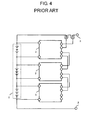
- FIG. 4 is a circuit diagram of a battery device which outputs a conventional high voltage.
- charging/discharging thereof has been controlled by a voltage generator 1 in which a plurality of secondary batteries are connected in series, and a plurality of voltage monitoring devices 2 (refer to, for example, Patent Document 1).
- Patent Document 1 Japanese Patent Application Laid-Open No. 2009-195100
- the secondary batteries equivalent to the number required to obtain a predetermined voltage are connected in series.
- the higher the required voltage the more the number of the secondary batteries increases, thus resulting in high cost of the battery device.
- the voltage monitoring devices 2 corresponding to the number of the secondary batteries are required. Further, a problem arises in that when a plurality of secondary batteries are used, a difference in potential between the secondary batteries occurs so that the charging time of the battery device and the discharging time thereof become short, thus resulting in the shortening of the life of the battery device.
- one aspect of a booster apparatus of the present invention is configured as follows:
- a booster apparatus includes a voltage generator, a plurality of boosting capacitors connected in series with the voltage generator, intermediary capacitors, and switch circuits configured to perform switching control of connections between the voltage generator, the plurality of boosting capacitors and the intermediary capacitors.
- a booster apparatus which performs boosting to a predetermined voltage required as a battery device only by one or necessary minimum voltage generators such as secondary batteries can be provided by the configuration of capacitors and switch circuits. Further, since a monitoring device for the voltage generator may also be connected only by the number of the voltage generators, an inexpensive booster apparatus can be realized. There can be provided a booster apparatus which needs not to consider a voltage difference generated upon series-connecting voltage generators since the number of the voltage generators may be one or the necessary minimum, and is capable of obtaining equimultiple boosted voltages at the voltage generators.
- FIG. 1 is a circuit diagram of a booster apparatus according to a first embodiment
- FIG. 2 is a circuit diagram of a switch circuit
- FIG. 3 is a circuit diagram of a booster apparatus according to a second embodiment.
- FIG. 4 is a circuit diagram of a related art battery device.
- FIG. 1 is a circuit diagram of a booster apparatus according to a first embodiment.
- the booster apparatus according to the first embodiment is equipped with a voltage generator 101 such as a secondary battery, capacitors 102 _ 1 through 102 _ 3 , capacitors 103 _ 1 and 103 _ 2 , and switch circuits 104 _ 1 through 104 _ 3 .
- a voltage generator 101 such as a secondary battery
- capacitors 102 _ 1 through 102 _ 3 capacitors 103 _ 1 and 103 _ 2
- switch circuits 104 _ 1 through 104 _ 3 switch circuits
- the capacitors 102 _ 1 through 102 _ 3 are boosting capacitors for allowing a battery device to generate a predetermined voltage.
- the capacitors 103 _ 1 and 103 _ 2 are intermediary capacitors for charging the voltage of the voltage generator 101 to the boosting capacitors 102 _ 1 through 102 _ 3 .
- the switch circuits 104 _ 1 through 104 _ 3 are control circuits which respectively switch connections between the capacitors 102 _ 1 through 102 _ 3 and the capacitors 103 _ 1 and 103 _ 2 to boost the voltage of the voltage generator 101 .
- FIG. 2 A circuit diagram of the switch circuit 104 is illustrated in FIG. 2 .
- the switch circuit 104 is equipped with connection terminals 105 through 107 , switches 111 through 113 , a connection terminal 108 , a switch control input terminal 109 , and a switch control output terminal 110 .
- the voltage generator 101 has a negative power supply terminal connected to the connection terminal 105 of the switch circuit 104 _ 1 and a positive power supply terminal connected to a negative power supply terminal of the boosting capacitor 102 _ 1 , the connection terminal 106 of the switch circuit 104 _ 1 , and the connection terminal 105 of the switch circuit 104 _ 2 .
- a positive power supply terminal of the boosting capacitor 102 _ 1 is connected to a negative power supply terminal of the boosting capacitor 102 _ 2 , the connection terminal 107 of the switch circuit 104 _ 1 , the connection terminal 106 of the switch circuit 104 _ 2 , and the connection terminal 105 of the switch circuit 104 _ 3 .
- a positive power supply terminal of the boosting capacitor 102 _ 2 is connected to a negative power supply terminal of the boosting capacitor 102 - 3 , the connection terminal 107 of the switch circuit 104 _ 2 , and the connection terminal 106 of the switch circuit 104 _ 3 .
- a positive power supply terminal of the boosting capacitor 102 _ 3 is connected to the connection terminal 107 of the switch circuit 104 _ 3 .
- a negative power supply terminal of the intermediary capacitor 103 _ 1 is connected to the connection terminal 108 of the switch circuit 104 _ 1 .
- a positive power supply terminal of the intermediary capacitor 103 _ 1 is connected to a negative power supply terminal of the intermediary capacitor 103 _ 2 and the connection terminal 108 of the switch circuit 104 _ 2 .
- a positive power supply terminal of the intermediary capacitor 103 _ 2 is connected to the connection terminal 108 of the switch circuit 104 _ 3 .
- the switch control input terminal 109 of the switch circuit 104 _ 1 is connected to a switch controller (unillustrated herein).
- the switch control output terminal 110 of the switch circuit 104 _ 1 is connected to the switch control input terminal 109 of the switch circuit 104 _ 2
- the switch control output terminal 110 of the switch circuit 104 _ 2 is connected to the switch control input terminal 109 of the switch circuit 104 _ 3 .
- the switch circuit 104 _ 1 When the switch circuit 104 _ 1 receives a control signal at the switch control input terminal 109 from the switch controller, the switch circuit 104 _ 1 sequentially and selectively switches ON/OFF of the switches 111 to 113 .
- the switch circuit 104 _ 2 receives a signal from the switch control output terminal 110 of the switch circuit 104 _ 1 at the switch control input terminal 109 thereof and is operated in such a manner that similar switches thereof are turned ON and OFF in synchronization.
- the switch circuit 104 _ 1 when the switch circuit 104 _ 1 receives a control signal at the switch control input terminal 109 from the switch controller, the switch circuit 104 _ 1 turns ON the switch 111 to short-circuit the connection terminal 105 and the connection terminal 108 . At this time, the switches 112 and 113 are OFF. Further, since the switch control input terminals 109 and the switch control output terminals 110 are connected in the switch circuits 104 _ 1 through 104 _ 3 , all of ON/OFF control of the switches become the same. Accordingly, the voltage generator 101 is connected in parallel with the intermediary capacitor 103 _ 1 by the switch 111 of the switch circuit 104 _ 1 and the switch 111 of the switch circuit 104 _ 2 .
- the intermediary capacitor 103 _ 1 becomes the same voltage as the voltage generator 101 .
- the boosting capacitor 102 _ 1 is connected in parallel with the intermediary capacitor 103 _ 2 by the switch 111 of the switch circuit 104 _ 2 and the switch 111 of the switch circuit 104 _ 3 .
- the boosting capacitor 102 _ 1 and the intermediary capacitor 103 _ 2 become the same voltage.
- the switch circuit 104 _ 1 when the switch circuit 104 _ 1 receives a control signal at the switch control input terminal 109 from the switch controller, the switch circuit 104 _ 1 turns ON the switch 112 to short-circuit the connection terminal 106 and the connection terminal 108 . At this time, the switches 111 and 113 are turned OFF. Further, other switch circuits 104 _ 2 and 104 _ 3 are similar. Thus, the boosting capacitor 102 _ 1 is connected in parallel with the intermediary capacitor 103 _ 1 by the switch 112 of the switch circuit 104 _ 1 and the switch 112 of the switch circuit 104 _ 2 . Consequently, the boosting capacitor 102 _ 1 becomes the same voltage as the intermediary capacitor 103 _ 1 . Likewise, the boosting capacitor 102 _ 2 becomes the same voltage as the intermediary capacitor 103 _ 2 .
- the switch circuit 104 _ 1 when the switch circuit 104 _ 1 receives a control signal at the switch control input terminal 109 from the switch controller, the switch circuit 104 _ 1 turns ON the switch 113 to short-circuit the connection terminal 107 and the connection terminal 108 . At this time, the switches 111 and 112 are turned OFF. Further, other switch circuits 104 _ 2 and 104 _ 3 are similar. Thus, the boosting capacitor 102 _ 2 becomes the same voltage as the intermediary capacitor 103 _ 1 . Likewise, the boosting capacitor 102 _ 3 becomes the same voltage as the intermediary capacitor 103 _ 2 .
- the switch circuit 104 _ 1 receives a control signal at the switch control input terminal 109 from the switch controller, the switch circuit 104 _ 1 turns ON the switch 111 to short-circuit the connection terminal 105 and the connection terminal 108 . At this time, the switches 112 and 113 are turned OFF.
- the four voltages of the voltage generator 101 are generated between the positive power supply terminal of the boosting capacitor 102 _ 3 and the negative power supply terminal of the voltage generator 101 by repeating the above operation. That is, the voltage generator 101 , the capacitors 102 and 103 , and the switch circuit 104 can configure the booster apparatus.
- the serial number of the boosting capacitors 102 is not limited, and the boosted voltage is also not limited.
- booster apparatus of the first embodiment there can be configured a booster apparatus which generates a predetermined voltage required as a battery device without increasing the number of voltage generators with a simple configuration based on one voltage generator, a plurality of capacitors connected in series therewith, intermediary capacitors, and switch circuits.
- a voltage monitoring device may be one.
- each boosting capacitor is allowed to generate the voltage of one voltage generator 101 through the intermediary capacitor, a booster apparatus can be configured without considering a voltage difference in the voltage generator.
- FIG. 3 is a circuit diagram of a booster apparatus according to a second embodiment.
- the booster apparatus according to the second embodiment is basically similar in configuration to the booster apparatus according to the first embodiment.
- the booster apparatus according to the second embodiment is comprised of a first boosting device 114 _ 1 and a second boosting device 114 _ 2 .
- the first boosting device 114 _ 1 is comprised of a voltage generator 101 _ 1 , boosting capacitors 102 _ 1 and 102 _ 2 , an intermediary capacitor 103 _ 1 , and switch circuits 104 _ 1 and 104 _ 2 .
- Each of the switch circuits 104 _ 1 and 104 _ 2 is the switch circuit 104 illustrated in FIG. 2 .
- the second boosting device 114 _ 2 also has a similar circuit configuration.
- the connections of the first boosting device 114 _ 1 and the second boosting device 114 _ 2 are similar to the booster apparatus according to the first embodiment. Then, the switch control output terminal 110 of the first boosting device 114 _ 1 and the switch control input terminal 109 of the second boosting device 114 _ 2 are connected to each other, and the boosting capacitor 102 _ 2 of the first boosting device 114 _ 1 and the voltage generator 101 _ 2 of the second boosting device 114 _ 2 are connected to each other.
- the operation of the booster apparatus according to the second embodiment is basically similar to that of the booster apparatus according to the first embodiment.
- the booster apparatus according to the second embodiment is capable of generating voltages equivalent to six voltage generators between the positive power supply terminal of the boosting capacitor 102 - 4 and the negative power supply terminal of the voltage generator 101 _ 1 . That is, the booster apparatus according to the second embodiment is capable of obtaining boosted voltages equivalent to six voltage generators with less numbers of parts than the booster apparatus according to the first embodiment.
- the second embodiment has described the booster apparatus which obtains the boosted voltages equivalent to the six voltage generators, the vertically-arranged number of the boosting devices 114 is not limited and the boosted voltages are also not limited.
- each switch circuit is illustrated with the three switches taken as one unit, the number of the switches is not limited.
- booster apparatus of the second embodiment there can be configured a booster apparatus with less numbers of parts commensurate with a simple configuration based on minimal voltage generators, a plurality of boosting capacitors connected in series therewith, intermediary capacitors, and switch circuits.
- booster apparatus of the present invention there can be configured a booster apparatus without increasing the number of voltage generators with a simple configuration based on minimal voltage generators, a plurality of boosting capacitors connected in series therewith, intermediary capacitors, and switch circuits.
Landscapes
- Engineering & Computer Science (AREA)
- Power Engineering (AREA)
- Dc-Dc Converters (AREA)
- Keying Circuit Devices (AREA)
- Charge And Discharge Circuits For Batteries Or The Like (AREA)
Abstract
Description
Claims (2)
Applications Claiming Priority (2)
| Application Number | Priority Date | Filing Date | Title |
|---|---|---|---|
| JP2014064020A JP6266400B2 (en) | 2014-03-26 | 2014-03-26 | Booster |
| JP2014-064020 | 2014-03-26 |
Publications (2)
| Publication Number | Publication Date |
|---|---|
| US20150280551A1 US20150280551A1 (en) | 2015-10-01 |
| US9882469B2 true US9882469B2 (en) | 2018-01-30 |
Family
ID=54168251
Family Applications (1)
| Application Number | Title | Priority Date | Filing Date |
|---|---|---|---|
| US14/664,413 Active 2035-06-02 US9882469B2 (en) | 2014-03-26 | 2015-03-20 | Booster apparatus for a direct current voltage generator |
Country Status (5)
| Country | Link |
|---|---|
| US (1) | US9882469B2 (en) |
| JP (1) | JP6266400B2 (en) |
| KR (1) | KR20150111870A (en) |
| CN (1) | CN104953818B (en) |
| TW (1) | TWI654820B (en) |
Cited By (1)
| Publication number | Priority date | Publication date | Assignee | Title |
|---|---|---|---|---|
| US20180309308A1 (en) * | 2017-04-20 | 2018-10-25 | Ablic Inc. | Charge/discharge control circuit and battery apparatus |
Citations (5)
| Publication number | Priority date | Publication date | Assignee | Title |
|---|---|---|---|---|
| US20090085537A1 (en) * | 2006-03-29 | 2009-04-02 | Mitsubishi Denki Kabushiki Kaisha | Power supply apparatus |
| US20110037432A1 (en) | 2007-07-06 | 2011-02-17 | Seiko Instruments Inc. | Battery state monitoring circuit and battery device |
| US20120313556A1 (en) * | 2010-02-24 | 2012-12-13 | Oliver Heid | DC High Voltage Source and Particle Accelerator |
| US20130163302A1 (en) * | 2011-12-23 | 2013-06-27 | Abb Inc. | Dc-dc converter systems |
| US20140319919A1 (en) * | 2013-04-30 | 2014-10-30 | Futurewei Technologies, Inc. | Soft Switching Inverter Device and Method |
Family Cites Families (3)
| Publication number | Priority date | Publication date | Assignee | Title |
|---|---|---|---|---|
| JP3424398B2 (en) * | 1995-07-26 | 2003-07-07 | 松下電工株式会社 | Power converter |
| JP2011050208A (en) * | 2009-08-28 | 2011-03-10 | Japan Aerospace Exploration Agency | Output voltage adjusting device utilizing intermediate tap of switched capacitor system |
| JP2013046433A (en) * | 2011-08-22 | 2013-03-04 | Seiko Instruments Inc | Cell balance device and battery system |
-
2014
- 2014-03-26 JP JP2014064020A patent/JP6266400B2/en active Active
-
2015
- 2015-03-11 TW TW104107737A patent/TWI654820B/en not_active IP Right Cessation
- 2015-03-20 CN CN201510124544.3A patent/CN104953818B/en not_active Expired - Fee Related
- 2015-03-20 US US14/664,413 patent/US9882469B2/en active Active
- 2015-03-24 KR KR1020150040984A patent/KR20150111870A/en not_active Application Discontinuation
Patent Citations (5)
| Publication number | Priority date | Publication date | Assignee | Title |
|---|---|---|---|---|
| US20090085537A1 (en) * | 2006-03-29 | 2009-04-02 | Mitsubishi Denki Kabushiki Kaisha | Power supply apparatus |
| US20110037432A1 (en) | 2007-07-06 | 2011-02-17 | Seiko Instruments Inc. | Battery state monitoring circuit and battery device |
| US20120313556A1 (en) * | 2010-02-24 | 2012-12-13 | Oliver Heid | DC High Voltage Source and Particle Accelerator |
| US20130163302A1 (en) * | 2011-12-23 | 2013-06-27 | Abb Inc. | Dc-dc converter systems |
| US20140319919A1 (en) * | 2013-04-30 | 2014-10-30 | Futurewei Technologies, Inc. | Soft Switching Inverter Device and Method |
Cited By (2)
| Publication number | Priority date | Publication date | Assignee | Title |
|---|---|---|---|---|
| US20180309308A1 (en) * | 2017-04-20 | 2018-10-25 | Ablic Inc. | Charge/discharge control circuit and battery apparatus |
| US10910851B2 (en) * | 2017-04-20 | 2021-02-02 | Ablic Inc. | Overcurrent, overcharge, and overdischarge detection and responsive switch control |
Also Published As
| Publication number | Publication date |
|---|---|
| CN104953818A (en) | 2015-09-30 |
| CN104953818B (en) | 2019-04-23 |
| JP6266400B2 (en) | 2018-01-24 |
| TWI654820B (en) | 2019-03-21 |
| JP2015186434A (en) | 2015-10-22 |
| US20150280551A1 (en) | 2015-10-01 |
| KR20150111870A (en) | 2015-10-06 |
| TW201607224A (en) | 2016-02-16 |
Similar Documents
| Publication | Publication Date | Title |
|---|---|---|
| CN109863662B (en) | Power supply device and control method for power supply device | |
| JP6812889B2 (en) | Power supply | |
| JP4834842B2 (en) | Power control device | |
| US10044286B2 (en) | Power conversion system including plurality of power converters connected in parallel to load | |
| EP3242389B1 (en) | Power supply device for sub-module controller of mmc converter | |
| JP6296608B2 (en) | Uninterruptible power system | |
| EP3373438A1 (en) | Capacitor discharge device inside sub module of mmc converter | |
| US9787173B2 (en) | Multilevel converter | |
| JP6805933B2 (en) | Power supply | |
| CN111130162A (en) | Power supply apparatus | |
| US9882469B2 (en) | Booster apparatus for a direct current voltage generator | |
| US10148222B2 (en) | Inverter apparatus and solar energy grid-connected power generation system | |
| KR20190116004A (en) | Variable capacity power bank system | |
| KR102028254B1 (en) | Vehicle, in particular an electric vehicle or a hybrid vehicle, and method for charging an energy storage cell of a vehicle | |
| US11322947B2 (en) | Energy storage apparatus | |
| CA2954481C (en) | Cell system and control method for cell system | |
| JP6825460B2 (en) | Power supply | |
| CN108270211B (en) | Bidirectional power supply device with parallel protection and method thereof | |
| KR101594508B1 (en) | Power supply apparatus | |
| Chamarthi et al. | A nine level inverter based grid connected solar PV system with voltage boosting | |
| CN110907846B (en) | Test system and test method of DC/DC conversion module | |
| JP2015027125A (en) | On-vehicle charging device | |
| JP2018110478A (en) | Electric power system | |
| EA028369B1 (en) | Pulse modulator with enhanced reliability |
Legal Events
| Date | Code | Title | Description |
|---|---|---|---|
| AS | Assignment |
Owner name: SEIKO INSTRUMENTS INC., JAPAN Free format text: ASSIGNMENT OF ASSIGNORS INTEREST;ASSIGNORS:SAKURAI, ATSUSHI;SAITO, HIROSHI;SIGNING DATES FROM 20150727 TO 20150728;REEL/FRAME:036239/0511 |
|
| AS | Assignment |
Owner name: SII SEMICONDUCTOR CORPORATION ., JAPAN Free format text: ASSIGNMENT OF ASSIGNORS INTEREST;ASSIGNOR:SEIKO INSTRUMENTS INC;REEL/FRAME:037783/0166 Effective date: 20160209 |
|
| AS | Assignment |
Owner name: SII SEMICONDUCTOR CORPORATION, JAPAN Free format text: CORRECTIVE ASSIGNMENT TO CORRECT THE EXECUTION DATE PREVIOUSLY RECORDED AT REEL: 037783 FRAME: 0166. ASSIGNOR(S) HEREBY CONFIRMS THE ASSIGNMENT;ASSIGNOR:SEIKO INSTRUMENTS INC;REEL/FRAME:037903/0928 Effective date: 20160201 |
|
| STCF | Information on status: patent grant |
Free format text: PATENTED CASE |
|
| AS | Assignment |
Owner name: ABLIC INC., JAPAN Free format text: CHANGE OF NAME;ASSIGNOR:SII SEMICONDUCTOR CORPORATION;REEL/FRAME:045567/0927 Effective date: 20180105 |
|
| MAFP | Maintenance fee payment |
Free format text: PAYMENT OF MAINTENANCE FEE, 4TH YEAR, LARGE ENTITY (ORIGINAL EVENT CODE: M1551); ENTITY STATUS OF PATENT OWNER: LARGE ENTITY Year of fee payment: 4 |
|
| AS | Assignment |
Owner name: ABLIC INC., JAPAN Free format text: CHANGE OF ADDRESS;ASSIGNOR:ABLIC INC.;REEL/FRAME:064021/0575 Effective date: 20230424 |