US9231476B2 - Tracking energy consumption using a boost-buck technique - Google Patents
Tracking energy consumption using a boost-buck technique Download PDFInfo
- Publication number
- US9231476B2 US9231476B2 US13/874,608 US201313874608A US9231476B2 US 9231476 B2 US9231476 B2 US 9231476B2 US 201313874608 A US201313874608 A US 201313874608A US 9231476 B2 US9231476 B2 US 9231476B2
- Authority
- US
- United States
- Prior art keywords
- energy
- switch
- terminal
- circuit
- capacitor
- Prior art date
- Legal status (The legal status is an assumption and is not a legal conclusion. Google has not performed a legal analysis and makes no representation as to the accuracy of the status listed.)
- Active, expires
Links
Images


Classifications
-
- H—ELECTRICITY
- H02—GENERATION; CONVERSION OR DISTRIBUTION OF ELECTRIC POWER
- H02M—APPARATUS FOR CONVERSION BETWEEN AC AND AC, BETWEEN AC AND DC, OR BETWEEN DC AND DC, AND FOR USE WITH MAINS OR SIMILAR POWER SUPPLY SYSTEMS; CONVERSION OF DC OR AC INPUT POWER INTO SURGE OUTPUT POWER; CONTROL OR REGULATION THEREOF
- H02M3/00—Conversion of dc power input into dc power output
- H02M3/02—Conversion of dc power input into dc power output without intermediate conversion into ac
- H02M3/04—Conversion of dc power input into dc power output without intermediate conversion into ac by static converters
- H02M3/10—Conversion of dc power input into dc power output without intermediate conversion into ac by static converters using discharge tubes with control electrode or semiconductor devices with control electrode
- H02M3/145—Conversion of dc power input into dc power output without intermediate conversion into ac by static converters using discharge tubes with control electrode or semiconductor devices with control electrode using devices of a triode or transistor type requiring continuous application of a control signal
- H02M3/155—Conversion of dc power input into dc power output without intermediate conversion into ac by static converters using discharge tubes with control electrode or semiconductor devices with control electrode using devices of a triode or transistor type requiring continuous application of a control signal using semiconductor devices only
- H02M3/156—Conversion of dc power input into dc power output without intermediate conversion into ac by static converters using discharge tubes with control electrode or semiconductor devices with control electrode using devices of a triode or transistor type requiring continuous application of a control signal using semiconductor devices only with automatic control of output voltage or current, e.g. switching regulators
- H02M3/158—Conversion of dc power input into dc power output without intermediate conversion into ac by static converters using discharge tubes with control electrode or semiconductor devices with control electrode using devices of a triode or transistor type requiring continuous application of a control signal using semiconductor devices only with automatic control of output voltage or current, e.g. switching regulators including plural semiconductor devices as final control devices for a single load
- H02M3/1582—Buck-boost converters
-
- G—PHYSICS
- G01—MEASURING; TESTING
- G01R—MEASURING ELECTRIC VARIABLES; MEASURING MAGNETIC VARIABLES
- G01R21/00—Arrangements for measuring electric power or power factor
-
- G—PHYSICS
- G01—MEASURING; TESTING
- G01R—MEASURING ELECTRIC VARIABLES; MEASURING MAGNETIC VARIABLES
- G01R21/00—Arrangements for measuring electric power or power factor
- G01R21/133—Arrangements for measuring electric power or power factor by using digital technique
-
- G—PHYSICS
- G01—MEASURING; TESTING
- G01R—MEASURING ELECTRIC VARIABLES; MEASURING MAGNETIC VARIABLES
- G01R22/00—Arrangements for measuring time integral of electric power or current, e.g. electricity meters
- G01R22/06—Arrangements for measuring time integral of electric power or current, e.g. electricity meters by electronic methods
- G01R22/10—Arrangements for measuring time integral of electric power or current, e.g. electricity meters by electronic methods using digital techniques
Definitions
- the invention relates to an electronic device and a method for tracking the energy consumption, and more specifically to an electronic device and a method for determining energy consumption using the principle of storing energy in an inductor and transferring the energy into output energy storing components.
- One of the more common techniques for measuring a current is a measurement using a shunt device or a shunt resister.
- a shunt device for the power measurement requires very high precision analogue to digital converters in order to cover the full dynamic range of the possible magnitudes of the currents. For example, when four and a half decades of measurement with one percent precision is required, a 24-Bit-converter would be required.
- shunt devices generate a voltage drop. This voltage should be compensated, while the compensation circuitry constitutes a potential source of errors. Direct load compensation can be difficult. This means that the measurement range and therefore the circuitry used for measuring the power consumption has to be adapted during the energy measurement procedure. This increases complexity and entails more potential errors.
- measuring a current indirectly by measuring the voltage across a shunt device requires an initial voltage change on the target. If a buffer capacitor is coupled to the target side (output side of an energy transfer circuits), the buffer capacitor delivers current immediately and needs to be recharged. This behavior affects the true current response of the device under test.
- Another approach of measuring the energy consumption employs a current mirror. One side of the current mirror delivers the current to the target including the target capacitor. The other side of the current mirror is coupled to an Ampere meter to which the mirrored current is fed. This approach has the advantage that the distortion caused by the target capacitor is minimized.
- the required pairing of the power and sense field effect transistors (FET) is rather poor and is not capable of tracking the huge current magnitude to be supported.
- an electronic device 200 comprises switched mode energy tracking circuitry.
- the switched mode circuitry comprises one or more switching elements SWA-SWB, SW 1 a -SW 1 b and SWia-SWib, one or more in inductors, LA-Li, a capacitor CA and compare circuits 406 and 434 that control the output voltage level VO and the output voltage level V 1 respectively.
- the switching elements, SWA-SWia are configured to switch current through the inductors LA-Li respectively respectively.
- the switches, SWA-SWB, SW 1 a -SW 1 ia and SW 1 b -SW 1 ib may be transistors.
- the voltage compare circuits 406 and 434 may be error amplifiers, a voltage comparators, or an A/D converters which conversion result is compared to a reference voltage VL(ref).
- the ON/OFF generator 408 is configured to control the ON-time and OFF-time of the switching elements, SW 1 a -SW 1 ia and SW 1 b -SW 1 ib , in order to transfer energy from a primary energy source, e.g. power supply, to the output VO of the energy tracking system and to control the level of the output voltage VO.
- the electronic device 200 further comprises control logic stages CNTLA, CNTL 1 and CTNLi.
- a control block 410 comprises an error handling block 420 , reporting block 416 , a calibration block 428 , an accumulator 430 of the individual ON-time events, a sequencing block 422 , a range control block 418 and a demand control block 424 .
- the control logic stages CTNLA-CNTLi generate the switching signals SWSA, SWS 1 a to SWSib for the switched transistors, SWA-SWB, SW 1 a -SW 1 ia and SW 1 b -SW 1 ib , in the form of ON-time pulses with a constant width ON-time.
- the control logic stages, CTNLA-CNTLi also control the OFF-time which is used also as an indicator of the energy in the inductors that is transferred to the output VO.
- the voltage-compare circuits 406 and 432 flag when the next ON-time pulse has to be generated. If the OFF-time is not over before the next ON-time is triggered, the system reports an error condition. An error condition is also reported if the output voltage VL is not within predefined limits.
- the switching signals, SWS 1 a to SWSib, are formed according to a pulse density scheme.
- the highest density of pulses occurs when the On-time and OFF-time are met at the time another ON-time is requested. Higher density is enabled by default or by control information (e.g. a control bit and this is handled by the control circuit as described previously).
- the pulse accumulator 430 can be in the simplest implementation a digital counter.
- the counter in this embodiment is then configured to count the number of ON-time pulses for determining the consumed power based on the number of ON-time pulses per time.
- the constant pulse width of the ON-time pulses makes the influence of the system components such as the non-linear behavior of switched transistors or inductors negligible.
- the target voltage offset at the output of the energy tracking system is highly reduced. A wide range of magnitudes of the measured current can be covered.
- the electronic device comprises a first capacitor C 1 coupled to the input of the energy tracking system, a second capacitor CA at the input of the energy tracking blocks 204 and 206 and a third capacitor C 2 coupled to the output of the energy tracking system.
- the ON-time of the switching element in conjunction with the inductor's L 1 value and the value of the capacitor CA is configured to keep the voltage within the system accuracy requirements.
- the output capacitor C 2 is of such value that the voltage increase during transferring the energy from the inductor L 1 to Li is within the accuracy expectations.
- the energy tracking system of this embodiment is contrary to a pulse width modulation scheme and nearly all energy in the inductors, L 1 -Li can be transferred to capacitor C 2 .
- the frequency of the ON-time pulses is proportional to and practically a linear function of the consumed current.
- each ON-time pulse of the switched transfers about the same amount of energy.
- a reference impedance 205 or a reference resistor R can be coupled to the output of the energy tracking system in order to make a reference energy measurement.
- the results of the reference measurement(s) can then be used for calibrating the system to the energy consumption. Therefore, the number of the ON-time pulses can be used for determining the energy consumption during normal operation even with an unknown load (e.g. C 3 & Z).
- the unknown load according to an embodiment of the invention can be an electronic device.
- the electronic device 200 comprises an energy tracking system with switching components SWA-SWB, SW 1 a -SW 1 ia and SW 1 b -SW 1 ib , inductors LA, L 1 , Li, transfer support diodes DA-Di.
- the switching components SWA-SW 1 ia can then be configured to enable current through the inductors LA-Li respectively.
- the optional switches SWB-SWib may be used to conduct current during the OFF-time to support the transfer of energy from an inductor to the output.
- the optional switch SWB does not conduct energy after the energy transfer is completed preventing that energy from flowing back from the output to the input.
- the optional switches SW 1 b -SWib do not conduct energy after the energy transfer is completed preventing that energy from flowing from the output to ground.
- the voltage compare circuits 406 and 434 can be error comparators or error amplifiers.
- the voltage compare circuit 406 is configured to send a signal 426 to the control circuit 410 and the ON/OFF generator 408 so that the switching components SW 1 a -SW 1 ia and SW 1 b -SW 1 ib can be triggered or be prepared to be triggered.
- the compare circuits 406 and 434 serve to deliver the demand on energy to maintain a stable output voltage VO and V 1 respectively.
- the generation and frequency of the ON-time pulses can be controlled in response to a change of the output voltages VO.
- the ON-time pulses can be combined with a time stamp on an individual basis or on a group of pulses.
- Another embodiment of the invention includes ON-time pulses that are based on a defined time and the difference to that defined time base is bounded by pulses or a group of pulses. The energy consumption may then be determined based on the number of the ON-time pulses per considered time period.
- the energy consumption may then be derived from a phase variation of the ON-time pulses.
- This aspect allows a quick evaluation of changes of the power consumption.
- the energy transfer during ON-time pulses usually is significantly smaller than the energy stored on a second capacitor CA coupled to the input of the energy transfer system.
- the energy withdrawn from the energy source at the input of the energy transfer system influences the energy transferred during the ON-time.
- the influence of the energy sourcing capability is a factor in the calibration cycle.
- the energy stored on a second capacitor C 2 coupled to the output of the energy transfer system is also significantly larger than the energy stored in the inductor during the ON-time and transferred to the output and the capacitor C 2 during OFF-time.
- the energy consumption may be calibrated by coupling one or more reference impedances 205 to the output of the energy transfer system. The result of the calibration may then be used for normalizing the energy consumption during normal operation.
- a target device or a device under test (DUT) 208 is then coupled to the output of the energy transfer system instead of the reference impedance 205 .
- the reference impedance 205 may be coupled to the output while the target load device or DUT 208 is still coupled to the output.
- the energy of one or a group of ON-time pulses due to the additional load of the reference load can be evaluated for calibrating the power measurement based on the energy pulse ON-time and OFF-time conditions.
- FIG. 1 shows a circuit measuring the current, the voltage and the timing relations to calculate the energy consumed within the load of the device-under-test.
- FIG. 2 a is a simplified circuit diagram of an embodiment of the invention.
- FIGS. 2 b and 2 c are simplified circuit diagrams of an embodiment of the invention.
- FIG. 3 is a diagram showing waveforms of signals of the circuit shown in FIG. 2 a according to an embodiment of the invention.
- FIG. 4 is a circuit diagram of an embodiment of the invention.
- FIG. 1 shows a circuit 101 that measures the load current via a voltage-to-voltage converter 102 , an A/D converter 104 and timer 106 .
- the energy EL used by the load is calculated in block EL 108 .
- the voltage VL is measured via the A/D converter 104 .
- phase related errors may occur.
- a timer 106 is used to create the time base t(b) for the A/D converter 104 .
- the energy EL used by the load i.e. DUT
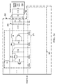
- FIG. 2 a shows a simplified diagram of an embodiment of the invention.
- an energy tracking system 200 comprises energy transfer blocks 202 , 204 , 206 , a control circuit 201 and reference impedance 205 .
- energy transfer block 202 is a “boost” circuit that comprises switched transistors SWA and SWB, diode DA, capacitor CA and inductor LA.
- energy transfer blocks 204 and 206 are “buck” circuits.
- Energy transfer block 204 comprises switched transistors SW 1 a and SW 1 b , diode D 1 , and inductor L 1 .
- Energy transfer block 206 comprises switched transistors SWia and SWib, diode Di, and inductor Li.
- two buck energy transfer blocks 204 and 206 are shown. However, more than two buck energy transfer blocks may be used.
- boost block 202 one terminal of inductor LA is coupled to a first switched transistor SWA, a second switched transistor SWB and to the anode of diode DA.
- the other terminal of the inductor LA is coupled to an input of the energy transfer block 202 .
- the cathode of the diode DA, a terminal of the capacitor CA and a terminal of the second switched transistor SWB are connected to an output of the boost block 202 .
- a terminal of the capacitor CA and a terminal of the first switched transistor SWA are connected to ground.
- the switched transistors SWA and SWB can be referred to as energizing switches.
- the diode DA may be replaced or complemented by the second switch SWB.
- the control circuit 201 controls the energy switches SWSA and SWSB.
- a function of boost block 202 is to transfer or “boost” the voltage on the input to a higher voltage level in order to have enough voltage margin for energy tracking blocks 204 and 206 .
- the control circuit 201
- one terminal of inductor L 1 is coupled to a first switched transistor SW 1 a , a second switched transistor SW 1 b and to the cathode of diode D 1 .
- the other terminal of the inductor L 1 is coupled to the output of the energy transfer block 204 .
- the anode of the diode D 1 and a terminal of the second switched transistor SW 1 b are connected to ground.
- a terminal of the first switched transistor SW 1 a is connected to the input of buck energy transfer block 204 .
- the switched transistors SW 1 a and SW 1 b can be referred to as energizing switches.
- the diode D 1 may be replaced or complemented by the second switch SW 1 b .
- the control circuit 201 controls the energy switches SWS 1 a and SWS 1 b .
- the control circuit 201 will be explained in more detail later in the specification.
- buck energy transfer block 206 one terminal of inductor Li is coupled to a first switched transistor SWia, a second switched transistor SWib and to the cathode of diode Di.
- the other terminal of the inductor Li is coupled to the output of the energy transfer block 206 .
- the anode of the diode Di and a terminal of the second switched transistor SWib are connected to ground.
- a terminal of the first switched transistor SWia is connected to the input of buck energy transfer block 206 .
- the switched transistors SWia and SWib can be referred to as energizing switches.
- the diode Di may be replaced or complemented by the second switch SWib.
- the control circuit 201 controls the energy switches SWSia and SWSib. The control circuit 201 will be explained in more detail later in the specification.
- FIG. 2 b shows a simplified diagram of an embodiment of the invention.
- an energy tracking system 200 comprises energy transfer blocks 209 , 211 , a control circuit 201 and reference impedance 205 .
- energy transfer blocks 209 and 211 are “boost-buck” circuits. In this example two boost-buck energy transfer blocks 209 and 211 are shown. However, more than two boost-buck energy transfer blocks may be used.
- one terminal of inductor L 1 a is coupled to a first switched transistor SW 1 a , a second switched transistor SW 1 b and to the anode of diode D 1 a .
- the other terminal of the inductor L 1 a is coupled to an input of the energy transfer block 209 .
- the cathode of the diode D 1 a , a terminal of the capacitor C 1 a , a terminal of the second switched transistor SW 1 b and a terminal of the third switched transistor SW 1 c are connected together.
- a terminal of the capacitor C 1 a , a terminal of the first switched transistor SW 1 a , the anode of diode D 1 b and a terminal of the fourth switched transistor SW 1 d are connected to ground.
- a terminal of inductor L 1 b is coupled to a terminal of the third switched transistor SW 1 c , a terminal of the fourth switched transistor SW 1 d and to the cathode of diode D 1 b .
- the other terminal of the inductor L 1 b is coupled to the output of the energy transfer block 209 .
- the switched transistors SWS 1 a , SWS 1 b , SWS 1 ic and SWS 1 d can be referred to as energizing switches.
- the diode D 1 a may be replaced or complemented by the second switch SW 1 b .
- the diode D 1 b may be replaced or complemented by the fourth switch SW 1 d .
- the control circuit 201 controls the energy switches SWS 1 a , SWS 1 b , SWS 1 c and SWS 1 d .
- the control circuit 201 will be explained in more detail later in the specification.
- one terminal of inductor Lia is coupled to a first switched transistor SWia, a second switched transistor SWib and to the anode of diode Dia.
- the other terminal of the inductor Lia is coupled to an input of the energy transfer block 211 .
- the cathode of the diode Dia, a terminal of the capacitor Cia, a terminal of the second switched transistor SWib and a terminal of the third switched transistor SWic are connected together.
- a terminal of the capacitor Cia, a terminal of the first switched transistor SWia, the anode of diode Dib and a terminal of the fourth switched transistor SWid are connected to ground.
- a terminal of inductor Lib is coupled to a terminal of the third switched transistor SWic, a terminal of the fourth switched transistor SWid and to the cathode of diode Dib.
- the other terminal of the inductor Lib is coupled to the output of the energy transfer block 209 .
- the switched transistors SWSia, SWSib, SWSic and SWSid can be referred to as energizing switches.
- the diode Dia may be replaced or complemented by the second switch SWib.
- the diode Dib may be replaced or complemented by the fourth switch SWid.
- the control circuit 201 controls the energy switches SWSia, SWSib, SWSic and SWSid. The control circuit 201 will be explained in more detail later in the specification.
- FIG. 3 shows the timing diagram for an energy transfer circuit (shown in FIG. 2 a ) that has two transfer paths.
- the first path has SW 1 a , L 1 , D 1 , and the ON-time signal SWS 1 a applied to SW 1 a .
- the switch SW 1 b shown in energy transfer block 204 is not used.
- the second path has SWia, Li, Di, and the ON-time signal SWSia applied to SWia.
- the switch SWSib shown in energy transfer block 206 in this example, is not used.
- the two energy transfer paths are used mainly to enhance the dynamic range of delivering energy.
- the optional switches SW 1 b and SWib may be used to conduct current during the OFF-time to support the transfer of energy from the inductors to the output.
- the optional switches SW 1 b and SWib do not conduct energy after the energy transfer is completed preventing that energy from flowing back from the output to the input.
- the system may have more than 2 paths enabling further spread of the dynamic range of the energy tracking circuits.
- FIG. 4 shows more detail in the control circuit 201 .
- the compare circuits 406 and 434 are coupled to receive a reference signal VL(ref) that is used to determine the output voltages VL and V 1 .
- the output of the compare circuits 406 and 423 are coupled to the control logic stages CNTLA 432 , CNTL 1 402 and CNTLi 404 .
- the ON-time and OFF-time generator 408 is coupled to feed the ON-time signals TG 1 and TGi to the control logic CNTL 1 and CNTLi respectively.
- the control logic stage CNTLA provides switching signals SWSA and SWSB for switching the switching element SWA and SWB to generate the voltage V 1 .
- the control logic stage CNTL 1 provides switching signals SWS 1 a and SWS 1 b with constant width ON-time pulses for switching the switching element SW 1 a and SW 1 b .
- the control logic stage CNTLi provides switching signals SWS 1 ia and SWSib with constant width ON-time pulses for switching the switching element SWia and SWib.
- the primary side of the energy tracking system is coupled to a first capacitor C 1 . Accordingly, one side of the inductor LA is coupled to one side of the first capacitor CA. The other side of the first capacitor CA is coupled to ground.
- the primary side of the energy tracking system is supplied by a stable supply realized by the circuit 202 .
- the output or secondary side of the energy tracking system is coupled to a second capacitor C 2 for buffering the output voltage VO.
- a target board or device under test 208 can be coupled to the output of the energy tracking system.
- the current consumed by the target board or device under test is the load current IL
- the level of the output voltage is VO.
- One or more reference impedances 205 in the form of reference resistor R and a switch LS can be coupled through switch LS to the energy tracking system.
- the reference resistor R can be switched to the output VO.
- the target board or DUT may still be coupled to the output during the reference measurement.
- the result of the reference measurement with the well characterized reference resistor R can then be used to calibrate the measurement for the operation with the unknown load (e.g. C 3 & Z) of the target board 208 .
- the energy transferred through the switched transistors SW 1 and SWi during an ON-time pulse is usually much smaller than the stored on the capacitors CA and C 2 .
- ESW energy that is transferred during an ON-time pulse
- the energy on capacitor CA is ECA
- the energy on capacitor C 1 is EC 1
- the energy on capacitor C 2 is EC 2
- the compare block 426 measures any deviation of target output voltage VL and versus VL(ref).
- the control blocks CNTL 1 and CNTLi increase or decrease the density of ON-time pulses.
- the ON-time pulses are generated with a constant width ON-time and a minimum OFF-time.
- the inductors L 1 , and Li will be charged with a certain amount of energy from the second capacitor CA. During the OFF-time the energy in the inductors is transferred to the third capacitor C 2 .
- the second capacitor CA and the third capacitor C 2 are sized such that this energy transfer does not significantly change the voltages across the second capacitor CA and the third capacitor C 2 .
- the compare block will not request another ON-time pulse through switching signal SWS 1 a , SWS 1 b or SWSia, SWSib.
- Another ON-time pulse will then be generated.
- each ON-time pulse represents approximately the same amount of energy that is transferred during each ON-time pulse.
- the OFF-time variations of the ON-time pulses of the switching signal SWSi 1 and SWSia also indicate current variations of the load currents IL.
- a reference measurement on the known reference resistor R can be used for normalizing the measured current.
- the reference resistors R may be switched on through switch LS in addition to the target board 208 .
- the influence of the reference resistor R on the OFF-time in signals SWS 1 a and SWSia can then be evaluated.
- the achieved result can be improved if the reference resistor R is switched on while the target board is not connected.
- FIG. 3 shows a diagram with waveforms of the load current IL, the output voltage VO, and ON-time signals as applied to switches SW 1 a and SWS 2 a .
- the load current IL of the target or DUT increases at a certain point of time.
- the voltage VO at the output node OUT varies according to a saw tooth scheme around the target output voltage level.
- the pulse density of the ON-time pulses SWS 1 a and SWS 2 a increases at a certain point of time or starts (SWS 2 a ) depending on the extent of the load current IL.
- the voltage VO varies according to a saw tooth scheme around the target output voltage level (dashed line).
- the pulse density of the ON-time pulses increases after the load current IL increases. This change in density of ON-time pulses of both paths is evaluated.
Abstract
Description
ELx=IL*VL*t(b) where x={1 . . . i} Equation 1
EC1=k1*ESWA
and
ECA=k2*(ESW1+ . . . ESWi) where X={1 . . . i}
and
EC2=k3*(ESW1+ . . . ESWi) where X={1 . . . i}
with
k1>20, k2 and k3>50.
Claims (14)
Priority Applications (6)
| Application Number | Priority Date | Filing Date | Title |
|---|---|---|---|
| US13/874,608 US9231476B2 (en) | 2013-05-01 | 2013-05-01 | Tracking energy consumption using a boost-buck technique |
| CN201410174518.7A CN104133108B (en) | 2013-05-01 | 2014-04-28 | Use buck Technical Follow-Up energy consumption |
| CN201811338308.1A CN109490621B (en) | 2013-05-01 | 2014-04-28 | Tracking energy consumption using buck-boost techniques |
| US14/987,527 US9400296B2 (en) | 2013-05-01 | 2016-01-04 | Tracking energy consumption using a boost-buck technique |
| US15/218,404 US9866121B2 (en) | 2013-05-01 | 2016-07-25 | Tracking energy consumption using a boost-buck technique |
| US15/865,035 US10924018B2 (en) | 2013-05-01 | 2018-01-08 | Tracking energy consumption using a boost-buck technique |
Applications Claiming Priority (1)
| Application Number | Priority Date | Filing Date | Title |
|---|---|---|---|
| US13/874,608 US9231476B2 (en) | 2013-05-01 | 2013-05-01 | Tracking energy consumption using a boost-buck technique |
Related Child Applications (1)
| Application Number | Title | Priority Date | Filing Date |
|---|---|---|---|
| US14/987,527 Continuation US9400296B2 (en) | 2013-05-01 | 2016-01-04 | Tracking energy consumption using a boost-buck technique |
Publications (2)
| Publication Number | Publication Date |
|---|---|
| US20140327457A1 US20140327457A1 (en) | 2014-11-06 |
| US9231476B2 true US9231476B2 (en) | 2016-01-05 |
Family
ID=51805856
Family Applications (4)
| Application Number | Title | Priority Date | Filing Date |
|---|---|---|---|
| US13/874,608 Active 2033-06-29 US9231476B2 (en) | 2013-05-01 | 2013-05-01 | Tracking energy consumption using a boost-buck technique |
| US14/987,527 Active US9400296B2 (en) | 2013-05-01 | 2016-01-04 | Tracking energy consumption using a boost-buck technique |
| US15/218,404 Active US9866121B2 (en) | 2013-05-01 | 2016-07-25 | Tracking energy consumption using a boost-buck technique |
| US15/865,035 Active US10924018B2 (en) | 2013-05-01 | 2018-01-08 | Tracking energy consumption using a boost-buck technique |
Family Applications After (3)
| Application Number | Title | Priority Date | Filing Date |
|---|---|---|---|
| US14/987,527 Active US9400296B2 (en) | 2013-05-01 | 2016-01-04 | Tracking energy consumption using a boost-buck technique |
| US15/218,404 Active US9866121B2 (en) | 2013-05-01 | 2016-07-25 | Tracking energy consumption using a boost-buck technique |
| US15/865,035 Active US10924018B2 (en) | 2013-05-01 | 2018-01-08 | Tracking energy consumption using a boost-buck technique |
Country Status (2)
| Country | Link |
|---|---|
| US (4) | US9231476B2 (en) |
| CN (2) | CN109490621B (en) |
Cited By (4)
| Publication number | Priority date | Publication date | Assignee | Title |
|---|---|---|---|---|
| US20150015233A1 (en) * | 2013-07-12 | 2015-01-15 | Texas Instruments Deutschland Gmbh | Tracking energy consumption using a buck-boosting technique |
| US20160241078A1 (en) * | 2013-10-22 | 2016-08-18 | Toyota Jidosha Kabushiki Kaisha | Solar power generation device and control method of solar power generation device |
| US20180198370A1 (en) * | 2013-05-01 | 2018-07-12 | Texas Instruments Deutschland Gmbh | Tracking energy consumption using a boost-buck technique |
| US10819327B2 (en) | 2018-10-29 | 2020-10-27 | Samsung Electronics Co., Ltd. | Duty timing detector detecting duty timing of toggle signal, device including duty timing detector, and operating method of device receiving toggle signal |
Families Citing this family (6)
| Publication number | Priority date | Publication date | Assignee | Title |
|---|---|---|---|---|
| US9146263B2 (en) * | 2013-03-07 | 2015-09-29 | Texas Instruments Incorporated | Electronic device and method for tracking energy consumption |
| US9523724B2 (en) | 2013-04-05 | 2016-12-20 | Texas Instruments Incorporated | Tracking energy consumption using a boost technique |
| EP3195377B1 (en) * | 2014-08-13 | 2021-12-15 | D-Wave Systems Inc. | Method of forming superconducting wiring layers with low magnetic noise |
| JP6789654B2 (en) * | 2016-04-04 | 2020-11-25 | 東芝キヤリア株式会社 | Power supply |
| US10696571B2 (en) | 2016-10-20 | 2020-06-30 | Lawrence Livermore National Security, Llc | Multiple pulse charge transfer for capacitive deionization of a fluid |
| CN110854900B (en) * | 2019-09-27 | 2023-07-25 | 西安电子科技大学 | Power point tracking circuit cooperatively obtained by multiple energy sources |
Citations (21)
| Publication number | Priority date | Publication date | Assignee | Title |
|---|---|---|---|---|
| US5623187A (en) * | 1994-12-28 | 1997-04-22 | Philips Electronics North America Corporation | Controller for a gas discharge lamp with variable inverter frequency and with lamp power and bus voltage control |
| US6177786B1 (en) | 1998-03-31 | 2001-01-23 | Fujitsu Limited | Power supply apparatus and method of controlling power supply circuit |
| US6844739B2 (en) | 2001-03-09 | 2005-01-18 | National Institute Of Advanced Industrial Science And Technology | Maximum power point tracking method and device |
| US20050111243A1 (en) | 2003-11-25 | 2005-05-26 | Guang-Nan Tzeng | Method of reducing a ripple of a heavy loading pulse frequency modulated voltage regulator |
| US20060145678A1 (en) * | 2005-01-05 | 2006-07-06 | Fyre Storm, Inc. | Switching power converter employing pulse frequency modulation control |
| US7119525B1 (en) | 2005-08-29 | 2006-10-10 | Fujitsu Limited | Control circuit of DC—DC converter and its control method |
| US20080122499A1 (en) | 2006-08-31 | 2008-05-29 | Louis Frew | Multi-threshold reset circuit |
| US7609051B2 (en) | 2003-12-30 | 2009-10-27 | Austriamicrosystems Ag | Energy metering system |
| US20100207455A1 (en) * | 2009-02-13 | 2010-08-19 | Miasole | Thin-film photovoltaic power element with integrated low-profile high-efficiency DC-DC converter |
| US20100229915A1 (en) * | 2007-10-15 | 2010-09-16 | Ampt, Llc | Systems for Highly Efficient Solar Power |
| US20100264869A1 (en) * | 2009-04-17 | 2010-10-21 | Stephen Dubovsky | Maximum Power Point Tracking Charge Controller with Coupled Inductor Multi-phase Converter |
| US20110031925A1 (en) * | 2005-08-29 | 2011-02-10 | Simburger Edward J | Nanosatellite photovoltaic regulator |
| US20120126624A1 (en) * | 2010-11-19 | 2012-05-24 | Texas Instruments Incorporated | High efficiency wide load range buck/boost/bridge photovoltaic micro-converter |
| US20120293021A1 (en) * | 2011-03-22 | 2012-11-22 | Triune Ip Llc | Variable Power Energy Harvesting System |
| US8390261B2 (en) | 2010-05-21 | 2013-03-05 | Infineon Technologies Austria Ag | Maximum power point tracker bypass |
| US20130154372A1 (en) | 2011-12-14 | 2013-06-20 | Macroblock, Inc. | Power-factor-corrected resonant converter and parallel power-factor-corrected resonant converter |
| US20130249421A1 (en) * | 2012-03-24 | 2013-09-26 | Dialog Semiconductor Gmbh | Method for Optimizing Efficiency versus Load Current in an Inductive Boost Converter for White LED Driving |
| US20140003830A1 (en) * | 2012-07-02 | 2014-01-02 | Konica Minolta, Inc. | Image forming apparatus capable of accurately estimating power consumption level |
| US20140300343A1 (en) | 2013-04-05 | 2014-10-09 | Texas Instruments Incorporated | Tracking energy consumption using a sepic-converter technique |
| US20140300342A1 (en) | 2013-04-05 | 2014-10-09 | Texas Instruments Incorporated | Tracking energy consumption using a boost technique |
| US20140301112A1 (en) | 2013-04-05 | 2014-10-09 | Texas Instruments Incorporated | Tracking energy consumption using a fly-back converter technique |
Family Cites Families (40)
| Publication number | Priority date | Publication date | Assignee | Title |
|---|---|---|---|---|
| US5625549A (en) * | 1994-09-23 | 1997-04-29 | Kaman Electronics Corporation | Boost-buck rectifier bridge circuit topology with diode decoupled boost stage |
| JP3720772B2 (en) * | 2002-01-31 | 2005-11-30 | キヤノン株式会社 | Current determination circuit and image recording apparatus having current determination circuit |
| JP2005532028A (en) * | 2002-06-27 | 2005-10-20 | コーニンクレッカ フィリップス エレクトロニクス エヌ ヴィ | DC-DC converter |
| US6788033B2 (en) * | 2002-08-08 | 2004-09-07 | Vlt, Inc. | Buck-boost DC-DC switching power conversion |
| US6819011B2 (en) * | 2002-11-14 | 2004-11-16 | Fyre Storm, Inc. | Switching power converter controller with watchdog timer |
| CN100392969C (en) * | 2004-03-11 | 2008-06-04 | 纬创资通股份有限公司 | Boost installation |
| US20050275382A1 (en) * | 2004-06-09 | 2005-12-15 | Stessman Nicholas J | Charge consumption monitor for electronic device |
| CN1797892A (en) * | 2004-12-30 | 2006-07-05 | 中国科学院电工研究所 | Tracker for maximum power of light-volt electric-power production by solar energy, and control method |
| US7248027B2 (en) * | 2005-01-05 | 2007-07-24 | Fyresstorm, Inc. | Power converters in which the input power coupling times are adjusted in conjunction with cycle skip counts |
| JP4728687B2 (en) * | 2005-04-22 | 2011-07-20 | 日本電信電話株式会社 | Booster |
| WO2007003967A2 (en) * | 2005-07-06 | 2007-01-11 | Cambridge Semiconductor Limited | Switch mode power supply control systems |
| US8405367B2 (en) * | 2006-01-13 | 2013-03-26 | Enecsys Limited | Power conditioning units |
| TWI328730B (en) * | 2006-06-16 | 2010-08-11 | Ablerex Electronics Co Ltd | Maximum power point tracking method and tracker thereof for a solar power system |
| TW200842545A (en) * | 2007-04-24 | 2008-11-01 | Winbond Electronics Corp | Controlling apparatus for a power converter and controlling method thereof |
| US20080283118A1 (en) * | 2007-05-17 | 2008-11-20 | Larankelo, Inc. | Photovoltaic ac inverter mount and interconnect |
| US7903439B2 (en) * | 2007-05-18 | 2011-03-08 | Texas Instruments Incorporated | Methods and apparatus to control a digital power supply |
| TW200847593A (en) * | 2007-05-18 | 2008-12-01 | Richtek Techohnology Corp | Digital voltage transformer and its control method |
| ATE501545T1 (en) * | 2007-08-20 | 2011-03-15 | Austriamicrosystems Ag | DC CONVERTER ARRANGEMENT AND METHOD FOR DC CONVERSION |
| US20090086511A1 (en) * | 2007-09-27 | 2009-04-02 | Phison Electronics Corp. | Converter circuit with pulse width frequency modulation and method thereof |
| US7923974B2 (en) * | 2008-01-04 | 2011-04-12 | Chil Semiconductor Corporation | Modification of switch activation order in a power supply |
| US7888924B2 (en) * | 2008-02-08 | 2011-02-15 | Texas Instruments Incorporated | Combination continuous and discontinuous control of a power regulator |
| US7969133B2 (en) * | 2008-05-14 | 2011-06-28 | National Semiconductor Corporation | Method and system for providing local converters to provide maximum power point tracking in an energy generating system |
| JP2010038531A (en) | 2008-07-10 | 2010-02-18 | Ihi Corp | Heat treatment device |
| GB2481778B (en) * | 2009-04-16 | 2014-02-05 | Panoramic Power Ltd | Apparatus and methods thereof for power consumption measurement at circuit breaker points |
| US8354827B2 (en) * | 2009-06-03 | 2013-01-15 | Lincoln Global, Inc. | Controller for a buck-boost circuit |
| US8773084B2 (en) * | 2009-08-24 | 2014-07-08 | Micrel, Inc. | Buck-boost converter using timers for mode transition control |
| CN101795066B (en) * | 2009-11-24 | 2013-01-09 | 南京航空航天大学 | Interleaved switching method of Buck-Boost convertor and realization circuit thereof |
| CN101834458B (en) * | 2010-05-10 | 2012-10-17 | 重庆大学 | Photovoltaic maximum energy collection device based on dynamic topological structure and method thereof |
| US8634216B2 (en) * | 2010-07-08 | 2014-01-21 | Solarbridge Technologies, Inc. | Communication within a power inverter using transformer voltage frequency |
| US9035626B2 (en) * | 2010-08-18 | 2015-05-19 | Volterra Semiconductor Corporation | Switching circuits for extracting power from an electric power source and associated methods |
| CN102570804B (en) * | 2010-12-28 | 2015-02-25 | 台达电子工业股份有限公司 | DC (direct current) power supply conversion module and control method thereof as well as connector and energy collection system |
| CN102141817B (en) * | 2011-02-18 | 2012-10-03 | 电子科技大学 | Buck voltage stabilizing circuit with load minimum energy point tracking (MEPT) circuit |
| TWI463778B (en) * | 2011-04-29 | 2014-12-01 | Energy Pass Inc | Current mode buck-boost converter and direct current voltage converting method thereof |
| CN102520241B (en) * | 2011-12-26 | 2014-07-02 | 武汉盛帆电子股份有限公司 | Three-phase charge-controlled electric energy meter based on resistance-capacitance voltage reduction and low-voltage direct-current/direct-current (DC/DC) power supply |
| CN102751876A (en) * | 2012-07-18 | 2012-10-24 | 浙江大学 | Isolation type new energy power supply equipment based on three-port power converter |
| JP5806413B2 (en) * | 2012-10-23 | 2015-11-10 | 三菱電機エンジニアリング株式会社 | Power supply control device and control method for power supply control device |
| EP2731246A1 (en) * | 2012-11-08 | 2014-05-14 | Delphi Technologies, Inc. | Switching regulator |
| US9231476B2 (en) * | 2013-05-01 | 2016-01-05 | Texas Instruments Incorporated | Tracking energy consumption using a boost-buck technique |
| CN103280971B (en) * | 2013-05-28 | 2016-01-13 | 成都芯源系统有限公司 | Buck-boost converter and controller and control method thereof |
| US9618545B2 (en) * | 2013-07-12 | 2017-04-11 | Texas Instruments Incorporated | Tracking energy consumption using a buck-boosting technique |
-
2013
- 2013-05-01 US US13/874,608 patent/US9231476B2/en active Active
-
2014
- 2014-04-28 CN CN201811338308.1A patent/CN109490621B/en active Active
- 2014-04-28 CN CN201410174518.7A patent/CN104133108B/en active Active
-
2016
- 2016-01-04 US US14/987,527 patent/US9400296B2/en active Active
- 2016-07-25 US US15/218,404 patent/US9866121B2/en active Active
-
2018
- 2018-01-08 US US15/865,035 patent/US10924018B2/en active Active
Patent Citations (21)
| Publication number | Priority date | Publication date | Assignee | Title |
|---|---|---|---|---|
| US5623187A (en) * | 1994-12-28 | 1997-04-22 | Philips Electronics North America Corporation | Controller for a gas discharge lamp with variable inverter frequency and with lamp power and bus voltage control |
| US6177786B1 (en) | 1998-03-31 | 2001-01-23 | Fujitsu Limited | Power supply apparatus and method of controlling power supply circuit |
| US6844739B2 (en) | 2001-03-09 | 2005-01-18 | National Institute Of Advanced Industrial Science And Technology | Maximum power point tracking method and device |
| US20050111243A1 (en) | 2003-11-25 | 2005-05-26 | Guang-Nan Tzeng | Method of reducing a ripple of a heavy loading pulse frequency modulated voltage regulator |
| US7609051B2 (en) | 2003-12-30 | 2009-10-27 | Austriamicrosystems Ag | Energy metering system |
| US20060145678A1 (en) * | 2005-01-05 | 2006-07-06 | Fyre Storm, Inc. | Switching power converter employing pulse frequency modulation control |
| US20110031925A1 (en) * | 2005-08-29 | 2011-02-10 | Simburger Edward J | Nanosatellite photovoltaic regulator |
| US7119525B1 (en) | 2005-08-29 | 2006-10-10 | Fujitsu Limited | Control circuit of DC—DC converter and its control method |
| US20080122499A1 (en) | 2006-08-31 | 2008-05-29 | Louis Frew | Multi-threshold reset circuit |
| US20100229915A1 (en) * | 2007-10-15 | 2010-09-16 | Ampt, Llc | Systems for Highly Efficient Solar Power |
| US20100207455A1 (en) * | 2009-02-13 | 2010-08-19 | Miasole | Thin-film photovoltaic power element with integrated low-profile high-efficiency DC-DC converter |
| US20100264869A1 (en) * | 2009-04-17 | 2010-10-21 | Stephen Dubovsky | Maximum Power Point Tracking Charge Controller with Coupled Inductor Multi-phase Converter |
| US8390261B2 (en) | 2010-05-21 | 2013-03-05 | Infineon Technologies Austria Ag | Maximum power point tracker bypass |
| US20120126624A1 (en) * | 2010-11-19 | 2012-05-24 | Texas Instruments Incorporated | High efficiency wide load range buck/boost/bridge photovoltaic micro-converter |
| US20120293021A1 (en) * | 2011-03-22 | 2012-11-22 | Triune Ip Llc | Variable Power Energy Harvesting System |
| US20130154372A1 (en) | 2011-12-14 | 2013-06-20 | Macroblock, Inc. | Power-factor-corrected resonant converter and parallel power-factor-corrected resonant converter |
| US20130249421A1 (en) * | 2012-03-24 | 2013-09-26 | Dialog Semiconductor Gmbh | Method for Optimizing Efficiency versus Load Current in an Inductive Boost Converter for White LED Driving |
| US20140003830A1 (en) * | 2012-07-02 | 2014-01-02 | Konica Minolta, Inc. | Image forming apparatus capable of accurately estimating power consumption level |
| US20140300343A1 (en) | 2013-04-05 | 2014-10-09 | Texas Instruments Incorporated | Tracking energy consumption using a sepic-converter technique |
| US20140300342A1 (en) | 2013-04-05 | 2014-10-09 | Texas Instruments Incorporated | Tracking energy consumption using a boost technique |
| US20140301112A1 (en) | 2013-04-05 | 2014-10-09 | Texas Instruments Incorporated | Tracking energy consumption using a fly-back converter technique |
Non-Patent Citations (2)
| Title |
|---|
| United States Patent and Trademark Office, "Non-Final Office Action," issued in connection to U.S. Appl. No. 13/857,568, mailed Dec. 10, 2014 (18 pages). |
| United States Patent and Trademark Office, "Non-Final Office Action," issued in connection to U.S. Appl. No. 13/857,599, mailed Feb. 27, 2015 (9 pages). |
Cited By (10)
| Publication number | Priority date | Publication date | Assignee | Title |
|---|---|---|---|---|
| US20180198370A1 (en) * | 2013-05-01 | 2018-07-12 | Texas Instruments Deutschland Gmbh | Tracking energy consumption using a boost-buck technique |
| US10924018B2 (en) * | 2013-05-01 | 2021-02-16 | Texas Instruments Incorporated | Tracking energy consumption using a boost-buck technique |
| US20150015233A1 (en) * | 2013-07-12 | 2015-01-15 | Texas Instruments Deutschland Gmbh | Tracking energy consumption using a buck-boosting technique |
| US9618545B2 (en) * | 2013-07-12 | 2017-04-11 | Texas Instruments Incorporated | Tracking energy consumption using a buck-boosting technique |
| US10928427B2 (en) | 2013-07-12 | 2021-02-23 | Texas Instruments Incorporated | Tracking energy consumption using a buck-boosting technique |
| US11946961B2 (en) | 2013-07-12 | 2024-04-02 | Texas Instruments Incorporated | Tracking energy consumption using a buck-boosting technique |
| US20160241078A1 (en) * | 2013-10-22 | 2016-08-18 | Toyota Jidosha Kabushiki Kaisha | Solar power generation device and control method of solar power generation device |
| US10063090B2 (en) * | 2013-10-22 | 2018-08-28 | Toyota Jidosha Kabushiki Kaisha | Solar power generation device and control method of solar power generation device |
| US10819327B2 (en) | 2018-10-29 | 2020-10-27 | Samsung Electronics Co., Ltd. | Duty timing detector detecting duty timing of toggle signal, device including duty timing detector, and operating method of device receiving toggle signal |
| US11323110B2 (en) | 2018-10-29 | 2022-05-03 | Samsung Electronics Co., Ltd. | Duty timing detector detecting duty timing of toggle signal, device including duty timing detector, and operating method of device receiving toggle signal |
Also Published As
| Publication number | Publication date |
|---|---|
| US10924018B2 (en) | 2021-02-16 |
| US20140327457A1 (en) | 2014-11-06 |
| CN104133108A (en) | 2014-11-05 |
| US9866121B2 (en) | 2018-01-09 |
| US20180198370A1 (en) | 2018-07-12 |
| CN109490621A (en) | 2019-03-19 |
| CN109490621B (en) | 2021-07-23 |
| US20160116514A1 (en) | 2016-04-28 |
| US9400296B2 (en) | 2016-07-26 |
| US20160336860A1 (en) | 2016-11-17 |
| CN104133108B (en) | 2018-12-07 |
Similar Documents
| Publication | Publication Date | Title |
|---|---|---|
| US10924018B2 (en) | Tracking energy consumption using a boost-buck technique | |
| US10802058B2 (en) | Tracking energy consumption using a sepic-converter technique | |
| JP4735976B2 (en) | Power supply device and semiconductor test system using the same | |
| KR101326730B1 (en) | Calibration device for transformer monitoring module | |
| US7482829B2 (en) | Electric power applying circuit and test apparatus | |
| US11946961B2 (en) | Tracking energy consumption using a buck-boosting technique | |
| US9013203B2 (en) | Tracking energy consumption using a fly-back converter technique | |
| US10845832B2 (en) | Voltage-to-current converter | |
| US10613124B2 (en) | Electronic device and method for tracking energy consumption | |
| US10488443B2 (en) | Tracking energy consumption using a boost technique | |
| US20130154594A1 (en) | Electronic device and method for power measurement | |
| KR20220153292A (en) | BMS and Battery System | |
| US20220082629A1 (en) | Battery Current Measuring Device and Method | |
| US10650946B1 (en) | Trimming method of DCR sensing circuits | |
| JP2013088146A (en) | Testing device | |
| JP2001066349A (en) | Test device for electronic circuit |
Legal Events
| Date | Code | Title | Description |
|---|---|---|---|
| AS | Assignment |
Owner name: TEXAS INSTRUMENTS DEUTSCHLAND GMBH, GERMANY Free format text: ASSIGNMENT OF ASSIGNORS INTEREST;ASSIGNORS:DIEWALD, HORST;ZIPPERER, JOHANN;WEBER, PETER;AND OTHERS;REEL/FRAME:030325/0631 Effective date: 20130429 |
|
| STCF | Information on status: patent grant |
Free format text: PATENTED CASE |
|
| AS | Assignment |
Owner name: TEXAS INSTRUMENTS INCORPORATED, TEXAS Free format text: ASSIGNMENT OF ASSIGNORS INTEREST;ASSIGNOR:TEXAS INSTRUMENTS DEUTSCHLAND GMBH;REEL/FRAME:046865/0033 Effective date: 20180404 |
|
| MAFP | Maintenance fee payment |
Free format text: PAYMENT OF MAINTENANCE FEE, 4TH YEAR, LARGE ENTITY (ORIGINAL EVENT CODE: M1551); ENTITY STATUS OF PATENT OWNER: LARGE ENTITY Year of fee payment: 4 |
|
| AS | Assignment |
Owner name: TEXAS INSTRUMENTS INCORPORATED, TEXAS Free format text: ASSIGNMENT OF ASSIGNORS INTEREST;ASSIGNOR:TEXAS INSTRUMENTS DEUTSCHLAND GMBH;REEL/FRAME:055314/0255 Effective date: 20210215 |
|
| MAFP | Maintenance fee payment |
Free format text: PAYMENT OF MAINTENANCE FEE, 8TH YEAR, LARGE ENTITY (ORIGINAL EVENT CODE: M1552); ENTITY STATUS OF PATENT OWNER: LARGE ENTITY Year of fee payment: 8 |