US8923021B2 - Control circuit and system for switch mode power supply - Google Patents
Control circuit and system for switch mode power supply Download PDFInfo
- Publication number
- US8923021B2 US8923021B2 US13/338,857 US201113338857A US8923021B2 US 8923021 B2 US8923021 B2 US 8923021B2 US 201113338857 A US201113338857 A US 201113338857A US 8923021 B2 US8923021 B2 US 8923021B2
- Authority
- US
- United States
- Prior art keywords
- current
- controller
- signal
- power switch
- constant
- Prior art date
- Legal status (The legal status is an assumption and is not a legal conclusion. Google has not performed a legal analysis and makes no representation as to the accuracy of the status listed.)
- Active, expires
Links
Images


Classifications
-
- H—ELECTRICITY
- H02—GENERATION; CONVERSION OR DISTRIBUTION OF ELECTRIC POWER
- H02M—APPARATUS FOR CONVERSION BETWEEN AC AND AC, BETWEEN AC AND DC, OR BETWEEN DC AND DC, AND FOR USE WITH MAINS OR SIMILAR POWER SUPPLY SYSTEMS; CONVERSION OF DC OR AC INPUT POWER INTO SURGE OUTPUT POWER; CONTROL OR REGULATION THEREOF
- H02M1/00—Details of apparatus for conversion
- H02M1/36—Means for starting or stopping converters
-
- H—ELECTRICITY
- H02—GENERATION; CONVERSION OR DISTRIBUTION OF ELECTRIC POWER
- H02M—APPARATUS FOR CONVERSION BETWEEN AC AND AC, BETWEEN AC AND DC, OR BETWEEN DC AND DC, AND FOR USE WITH MAINS OR SIMILAR POWER SUPPLY SYSTEMS; CONVERSION OF DC OR AC INPUT POWER INTO SURGE OUTPUT POWER; CONTROL OR REGULATION THEREOF
- H02M1/00—Details of apparatus for conversion
- H02M1/0003—Details of control, feedback or regulation circuits
- H02M1/0025—Arrangements for modifying reference values, feedback values or error values in the control loop of a converter
-
- H—ELECTRICITY
- H02—GENERATION; CONVERSION OR DISTRIBUTION OF ELECTRIC POWER
- H02M—APPARATUS FOR CONVERSION BETWEEN AC AND AC, BETWEEN AC AND DC, OR BETWEEN DC AND DC, AND FOR USE WITH MAINS OR SIMILAR POWER SUPPLY SYSTEMS; CONVERSION OF DC OR AC INPUT POWER INTO SURGE OUTPUT POWER; CONTROL OR REGULATION THEREOF
- H02M3/00—Conversion of dc power input into dc power output
- H02M3/22—Conversion of dc power input into dc power output with intermediate conversion into ac
- H02M3/24—Conversion of dc power input into dc power output with intermediate conversion into ac by static converters
- H02M3/28—Conversion of dc power input into dc power output with intermediate conversion into ac by static converters using discharge tubes with control electrode or semiconductor devices with control electrode to produce the intermediate ac
- H02M3/325—Conversion of dc power input into dc power output with intermediate conversion into ac by static converters using discharge tubes with control electrode or semiconductor devices with control electrode to produce the intermediate ac using devices of a triode or a transistor type requiring continuous application of a control signal
- H02M3/335—Conversion of dc power input into dc power output with intermediate conversion into ac by static converters using discharge tubes with control electrode or semiconductor devices with control electrode to produce the intermediate ac using devices of a triode or a transistor type requiring continuous application of a control signal using semiconductor devices only
- H02M3/33507—Conversion of dc power input into dc power output with intermediate conversion into ac by static converters using discharge tubes with control electrode or semiconductor devices with control electrode to produce the intermediate ac using devices of a triode or a transistor type requiring continuous application of a control signal using semiconductor devices only with automatic control of the output voltage or current, e.g. flyback converters
Definitions
- Embodiments of the present invention are directed to power supply control circuits and power supply systems. More particularly, embodiments of the invention provide methods and circuits for controlling an output current in a switched mode power supply (SMPS).
- SMPS switched mode power supply
- Regulated power supplies are indispensable in modern electronics. For example, the power supply in a personal computer often needs to receive power input from various outlets. Desktop and laptop computers often have regulated power supplies on the motherboard to supply power to the CPU, memories, and periphery circuitry. Regulated power supplies are also used in a wide variety of applications, such as home appliances, automobiles, and portable chargers for mobile electronic devices, etc.
- a power supply can be regulated using a linear regulator or a switching mode controller.
- a linear regulator maintains the desired output voltage by dissipating excess power.
- a switching mode controller rapidly switches a power transistor on and off with a variable duty cycle or variable frequency and provides an average output that is the desired output voltage.
- Pulse Width Modulation PWM
- Pulse Frequency Modulation PFM
- green power supplies are emphasized, which require higher conversion efficiency and lower standby power consumption.
- PWM controlled switching mode power supply the system can be forced to enter into burst mode in standby conditions to reduce power consumption.
- PFM controlled switching mode power supply the switching frequency can be reduced in light load conditions.
- PFM-controlled switching mode power supply exhibits simple control topology and small quiescent current. Therefore, it is suitable for low cost small output power applications such as battery chargers and adapters.
- a switch In a switched mode power supply system, a switch is connected to the primary winding of the transformer. Magnetic energy is stored in the inductance of the primary winding when the switch is turned on, and the energy is transferred to the secondary winding when the switch is turned off. The energy transfer results in a current flowing through the secondary winding and the rectifying diode.
- the SMPS often operates in a constant-voltage mode or a constant-current mode. However, during start up, the constant-current mode can limit the output current and lead to long start up time.
- Embodiments of the present invention are directed to power supply control circuits and power supply systems. More particularly, embodiments of the invention provide methods and circuits for controlling an output current in a switched mode power supply (SMPS).
- SMPS switched mode power supply
- some embodiments of the invention have been applied to an SMPS controller such that the output current is increased during start up. But it would be recognized that the invention has a much broader range of applicability.
- a controller for a switched mode power supply (SMPS).
- the SMPS includes a transformer having a primary winding coupled to a power switch and a secondary winding for providing an output of the power supply.
- the controller includes a first input terminal for receiving a current sensing signal which is related to a current in the primary winding, a second input terminal for receiving a feedback signal related to a current in the secondary winding, and an output terminal for providing a power switch control signal to turn on and off the power switch.
- the controller is configured to cause the SMPS to maintain a constant output current at a first current magnitude.
- the controller When the feedback signal is lower than the first reference voltage, the controller is configured to cause the SMPS to provide a second output current at a second current magnitude higher than the first current magnitude. In a specific embodiment, when the feedback signal is higher than a second reference voltage that is higher than the first reference voltage, the controller is configured to cause the SMPS to maintain a constant output voltage. In some applications, the controller can be used to cause the power supply to provide a maximum output current at start up.
- a controller for a switched mode power supply (SMPS).
- the SMPS includes a transformer having a primary winding coupled to a power switch and a secondary winding for providing an output of the power supply.
- the controller includes a first input terminal for receiving a current sensing signal which is related to a current in the primary winding, a second input terminal for receiving a feedback signal related to a current in the secondary winding, and an output terminal for providing a power switch control signal to turn on and off the power switch.
- the controller is configured to cause the SMPS to maintain a constant output current at a first current magnitude.
- the controller When the feedback signal is lower than the first reference voltage, the controller is configured to cause the SMPS to provide a second output current at a second current magnitude higher than the first current magnitude.
- the controller When the feedback signal is higher than the second reference voltage that is higher than the first reference voltage, the controller is configured to cause the SMPS to maintain a constant output voltage.
- the controller described above can have a secondary conduction detection circuit configured to receive the feedback signal from the second input terminal and to generate a secondary conduction time signal, which is raised to a high value when a current is flowing in the secondary winding.
- the controller can also includes a constant-current control circuit configured to receive the secondary conduction time signal and to produce a constant current control signal that causes the power switch control signal to be activated at fixed intervals.
- the constant-current control circuit has a first capacitor configured to be charged with a source current through a source current switch and discharged with a sink current through a sink current switch and a comparator coupled to the first capacitor and configured to produce the constant current control signal.
- the controller also has a critical conduction control circuit that is configured to trigger the power switch control signal to turn on the power switch on a falling edge of the secondary conduction time signal when the feedback signal is lower than the first reference voltage.
- the critical conduction control circuit includes a comparator configured to receive the feedback signal and the first reference voltage. The comparator is enabled by the secondary conduction time signal.
- the critical conduction control circuit also has a flip-flop coupled to the comparator and a D-trigger circuit coupled to the flip-flop through one or more logic gates.
- the controller also includes a constant-voltage control circuit that is configured to trigger the power switch control signal when the feedback signal falls below a target output voltage.
- the controller can also have an off time control circuit configured to deactivate the power switch control signal when the current sense signal reaches a preset value.
- a switched mode power supply includes a primary winding, a power switch coupled to the primary winding, a secondary winding for providing an output of the power supply, and a controller coupled to the power switch.
- the controller has a first input terminal for receiving a current sensing signal which is related to a current in the primary winding, a second input terminal for receiving a feedback signal related to a current in the secondary winding, and an output terminal for providing a power switch control signal to turn on and off the power switch.
- the controller When the feedback signal is higher than a first reference voltage, the controller is configured to cause the SMPS to maintain a constant current at a first current.
- the controller is configured to cause the SMPS to provide a second current that is higher than the first current.
- FIG. 1 is a simplified block diagram illustrating a switch-mode power supply (SMPS) according to an embodiment of the present invention
- FIG. 2 is a simplified schematic diagram illustrating an SMPS according to an embodiment of the present invention
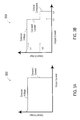
- FIG. 3A is a plot illustrating a plot of output voltage versus output current for an SMPS having two modes of operation
- FIG. 3B is a plot illustrating a plot of output voltage versus output current for an SMPS having three modes of operation according to an embodiment of the present invention
- FIG. 4 is a simplified block diagram illustrating some of the functions of an SMPS controller according to an embodiment of the present invention
- FIG. 5 is a schematic diagram illustrating an embodiment of control functions of an SMPS controller in constant-current mode
- FIG. 6 illustrates the waveforms of signals in the control circuit of FIG. 5 without a critical conduction mode
- FIG. 7 illustrates the waveforms of signals in the control circuit of FIG. 5 including a critical conduction mode.
- FIG. 1 is a simplified block diagram illustrating a switch-mode power supply (SMPS) 100 according to an embodiment of the present invention.
- power supply 100 includes a rectifying circuit 101 coupled to an input alternate current (AC) voltage source, a transformer 102 .
- the primary winding is coupled to rectifying circuit 101 .
- Power supply 100 also includes a power switch 103 couple to the transformer, and a control circuit 104 coupled to power switch 103 for controlling the current in the primary winding such that the power supply can output a constant output current.
- a transformer is included in this power supply, but a different inductance based coupling circuit can also be used.
- FIG. 2 is a simplified schematic diagram illustrating an SMPS 200 according to an embodiment of the present invention.
- a rectifying bridge 212 is coupled to an AC voltage source Vac.
- An energy storage capacitor C 1 is coupled to the rectifying bridge.
- One of the functions provided by capacitor C 1 is to reduce electromagnetic interference.
- a transformer 202 which includes a primary winding 221 , a secondary winding 222 , and an auxiliary winding 223 .
- the dots associated with the windings designate the same polarity.
- SMPS 200 also includes a control circuit 203 having the following terminals: FB for receiving a secondary winding conduction feedback signal, CS for receiving a signal related to the primary current, OUT for providing a driving signal to power switch 204 , VCC for connecting a power supply, and GND for connecting to an electrical ground.
- the FB terminal receives a signal reflecting the operating state of the secondary wining 222 and the output voltage through auxiliary winding 223 and voltage divider resistors R 1 and R 2 .
- the CS terminal receives a signal from sampling, current sensing, resistor R 5 about the primary current flow through power switch 204 and primary winding 221 .
- control circuit 203 receives information about current flow through power switch 204 from the CS terminal and information about secondary winding conduction operating state signal from the FB terminal.
- Control circuit 203 is configured to provide a control signal at the OUT terminal to control the on and off of power switch 204 .
- the output at secondary winding 222 is rectified, e.g., by rectifying diode D 1 , and provides at the power supply output terminal an output current Io and an output voltage Vout.
- control circuit 203 receives its operating power from auxiliary winding 223 through a rectifying diode D 2 and a capacitor C 2 .
- FIG. 3A is a plot illustrating a plot 300 of output voltage versus output current for an SMPS having two operating mode
- FIG. 3B is a plot 350 illustrating a plot of output voltage versus output current for an SMPS having three operating mode according to an embodiment of the present invention.
- an SMPS often operates in a constant-voltage mode or constant-current mode.
- the SMPS controller In the constant-voltage mode, the SMPS controller is configured to maintain the output at a target voltage.
- the controller examines the output voltage through a feedback signal and, if the output falls below the target, turns on the power switch to supply more current.
- the power switch can be turned off when, for example, the primary current reaches a certain level or after a fixed duration.
- the controller maintains a constant average output current.
- the constant-current mode is often used when the output load is low.
- the conventional constant-current mode operation is found to be not satisfactory, for example, during the start up phase of the power supply.
- FIG. 3A during start up, when the output voltage is close to zero, and the system is in a constant-current mode. As a result, the output current is fixed, which can lead to a long start up time.
- FIG. 3A shows that during start up, when the output voltage is close to zero, and the system is in a constant-current mode. As a result, the output current is fixed, which can lead to a long start up time.
- FIG. 3A shows that during start up, when the output voltage is close to zero, and the system is in a constant-current mode. As a result, the output current is fixed, which can lead to a long start up time.
- 3B illustrates a desirable output voltage versus output current plot provided by embodiments of the invention, in which the SMPS can still operates in a constant-voltage mode and a constant-current mode, but also has an enhanced phase in which the start up or low output voltage operation is improved.
- the output current is high, allowing a faster start up or a fast recovery from a low out put condition.
- the third mode operation is referred to as critical conduction mode.
- FIG. 4 is a simplified block diagram illustrating some of the functions of an SMPS controller according to an embodiment of the present invention.
- reference voltage generation circuit 402 is configured to provide a DC reference voltage, which is used to determine the peak current through the power switch.
- Power switch off time control circuit 403 is coupled to reference voltage generation circuit 402 and the input from the CS (current sense) terminal. When the voltage provided at the CS terminal reaches the above-mentioned reference voltage, the current in the primary winding is cut off.
- Secondary winding detection circuit 405 receives the feedback signal from the FB terminal to produce a voltage signal that reflects the current conduction in the secondary rectifying circuit.
- Power switch on time control circuit 406 determines the power switch on time based on charging a capacitor using a first current source and discharging the capacitor using a second current source.
- Power switch driver circuit 404 receives control signals from power switch off time control circuit 403 and power switch on time control circuit 406 and provides a control signal OUT to the power switch to turn it on and off. In constant-current mode, the ratio of the on time and off time is maintained at a constant.
- FIG. 5 is a schematic diagram illustrating an embodiment of an SMPS controller according 500 to an embodiment of the present invention. These functions are described with reference to the waveforms of relevant signals illustrated in FIGS. 6 and 7 .
- a secondary conduction detection circuit 505 receives feedback signal Vfb from the FB terminal and generates a secondary conduction time signal Tons that reflects the state of secondary rectifying circuit conduction. In some embodiment, Tons is at a high to indicate that a current is flowing in the secondary winding.
- secondary conduction detection circuit 505 includes a demagnetization detector (not shown) that compares feedback signal Vfb with a reference voltage (e.g., 0.1V) to detect the demagnetization of the primary winding. The demagnetization detector is coupled to a Tons detector (not shown), which produces the secondary conduction time signal Tons. The logic high state of secondary conduction time signal Tons is indicative of the secondary current flowing through the secondary winding.
- FIG. 5 also includes a constant-current control circuit 530 configured to receive the secondary conduction time signal Tons and to produce a constant current control signal (ON) that causes the power switch control signal OUT to be activated at fixed intervals.
- Tons when current flow is on in the secondary rectifying circuit, as represented by signal Tons, is at a high voltage level, and switch 509 is turned on.
- switch 508 In the mean time, switch 508 is turned off by Tons through inverter 506 . At this time, capacitor 511 is discharged by current source 510 .
- signal Tons is at a low voltage level
- switch 509 is turned off.
- switch 508 is turned on by Tons through inverter 506 . At this time, capacitor 511 is charged by current source 507 .
- the voltage at capacitor 511 during charging and discharging follows a triangular waveform.
- the ratio of on time to off time of the secondary rectifying circuit is determined by a constant determined by current sources 507 and 510 .
- the output of comparator 512 constant current control signal (ON) becomes high, causing the output Q of D-trigger 513 to be high, which in turn causes power switch 514 to output control signal OUT to turn on the power switch.
- the OUT signal will stay on until it is turned off by the off time control circuit 540 described below.
- D-trigger 513 receives an OFF_N signal and causes driver circuit 514 to deactivate the OUT signal for turning off the power switch.
- the OFF_N signal is produced by comparator 504 in off time control circuit 540 by comparing a reference signal VrefA from reference signal generator 502 and a signal from the CS terminal through leading edge blanking circuit 503 .
- the power switch is turned off when the current flow in the primary winding through the power switch reaches a reference value.
- leading edge blanking circuit (LEB) 503 includes a certain leading edge blanking time to block any spikes occurring at the sense resistor when the power switch is turned on.
- control circuit is further illustrated by the waveforms in FIG. 6 , which includes waveforms for the following signals.
- the Ton signal When secondary current Is reaches zero at 607 , the Ton signal is also drops to zero at point “A” in FIG. 6 After a delay, at point “B,” the OUT signal is turned high again to turn on the power switch and starts the next cycle.
- This delay is determined by constant-current control circuit 530 including capacitor 511 and current sources 507 and 510 .
- the time interval during which secondary current is not flowing is marked as Toff in FIG. 6 .
- the ratio of Ton to Toff is held constant, and so is the average secondary current is designated as Iavg in FIG. 6 . The cycle described above is repeated.
- Tons is the time during which secondary Is flows
- Ioff is the time during which secondary current Is is zero.
- A” and “B” designate two transition points of Vfb.
- Tons is the time during which secondary Is flows
- Ioff is the time during which secondary current Is is zero.
- A” and “B” designate two transition points of Vfb.
- the ratio of Ton to Toff is fixed, i.e., a constant duty cycle. It can be seen that during a substantial part of Toff, secondary current Is is zero. This condition is sometimes referred to as discontinuous current mode, which may be acceptable during normal operations. However, during start-up, when the currents are being built up, this mode of operation can lead to prolonged start-up time. The long start-up time may be unsatisfactory in some applications.
- embodiments of the invention also include a start up control circuit 520 as shown in FIG. 5 .
- critical conduction control circuit 520 is configured to trigger the power switch control signal to turn on the power switch on a falling edge of the secondary conduction time signal signal when the feedback signal is lower than a reference voltage.
- Critical conduction control circuit 520 includes a comparator 527 , a flip-flop 521 , a D-trigger 522 , inverters 523 and 524 , and an OR gate 525 .
- Comparator 527 receives Tons as an enable signal and compares the FB signal with a threshold reference voltage Vth 1 . Tons is also connected to the reset terminal of flip-flop 521 and OR gate 525 .
- Tons is low, and the output of D-trigger 522 is low.
- comparator 527 is enabled. If the voltage at FB does not reach threshold reference voltage Vth 1 , the output of D-trigger 522 is kept low. At the falling edge of the Tons signal, the output of D-trigger is raised to high, causing driver 514 to turn on the power switch.
- secondary current is lowered to zero at the trailing edge of Tons, the next on-cycle of the power switch is started.
- FIG. 7 illustrates the waveforms of signals in control circuit 500 of FIG. 5 including a critical conduction mode.
- the signals are the same as listed above in connection with FIG. 6 . It can be seen that the power switch is turned on at the trailing edge of the Tons signal, as soon as the secondary current reduces to zero.
- the time period Ton at point “A,” is followed immediately by a negative pulse, which is triggered by the OUT signal and indicates that primary current Ip is flowing.
- the Toff period includes a dead time during which no current is flowing, which is sometimes designated as a discontinuous mode of operation.
- there is little or no dead time between secondary current flow and primary current flow which is referred to as critical conduction current mode. In this mode of operation, the Toff period shown in FIG. 6 is substantially reduced. As a result, a higher output current can be obtained.
- FIG. 3B The operation depicted in FIGS. 5 and 7 and described above can be illustrate in FIG. 3B . It can be seen in FIG. 3B that when the output voltage is above a reference voltage V 1 , the system is in the constant-voltage mode in which the system is configured to maintain the output voltage at a target voltage. When the output voltage is below V 1 but above a second reference voltage V 2 , the system is in the constant-current mode, in which the current on-off time ratio is maintained at a constant, and the output current is maintained substantially at current I 1 . When the output voltage is below V 1 , the system enters the critical conduction mode, in which the primary current flow closely follows the secondary current and dead time is minimized.
- the output current is at a current I 2 , which is higher than I 1 .
- current I 2 is shown to be a constant current I 2 .
- the current in the critical conduction region may exhibit different current-voltage characteristics.
- the transition between different modes of operation is carried out by comparing Vfb with properly selected reference voltages.
- Vfb is higher than Vth 1 .
- the startup control circuit is not activated, and the constant-current mode operation takes over, in which a constant ratio of Ton to Toff is maintained.
- the constant-voltage mode is activated when Vfb is greater than a second threshold voltage.
- the SMPS controller is in a constant-voltage mode, when Vfb is greater than, e.g., 4V. When Vfb is below 4V, the controller is in constant-current mode. To speed up the start up of the power supply, the controller can enter critical conduction mode when Vfb is less than, e.g., 1V. In this case, at Vfb>1V, the system is in discontinuous mode and can be either in constant-voltage mode or constant-current mode. In another example, the controller may have only two modes of operation, i.e., in constant-current mode when Vfb>1V and in critical conduction mode when Vfb ⁇ 1V. Of course, there can be other variations.
- constant-current mode operation is similar to that of conventional SMPS, i.e., comparing Vfb with a target voltage and providing current to the output as needed.
- An example of constant-voltage mode operation is described in more detail in commonly owned U.S. patent application Ser. No. 12/620,420, filed Nov. 17, 2009, whose content is incorporated in its entirety by reference.
Landscapes
- Engineering & Computer Science (AREA)
- Power Engineering (AREA)
- Dc-Dc Converters (AREA)
Abstract
Description
-
- Vfb is the voltage signal at the FB terminal and represents the secondary side conduction state;
- Ip is the primary current, i.e., the current flowing in the primary winding;
- Is is the secondary current, i.e., the current flowing in the secondary winding;
- Vcs is the current sense voltage, which indicates the magnitude of primary current; and
- OUT is the control signal issued to the power switch from the SMPS controller.
Claims (20)
Priority Applications (1)
| Application Number | Priority Date | Filing Date | Title |
|---|---|---|---|
| US13/338,857 US8923021B2 (en) | 2009-11-17 | 2011-12-28 | Control circuit and system for switch mode power supply |
Applications Claiming Priority (5)
| Application Number | Priority Date | Filing Date | Title |
|---|---|---|---|
| US12/620,420 US8213203B2 (en) | 2009-03-20 | 2009-11-17 | Method and apparatus for controlling a constant current output in a switching mode power supply |
| CN201110409130.7 | 2011-12-09 | ||
| CN201110409130 | 2011-12-09 | ||
| CN201110409130.7A CN102497107B (en) | 2011-12-09 | 2011-12-09 | Switch power supply and controller of switch power supply |
| US13/338,857 US8923021B2 (en) | 2009-11-17 | 2011-12-28 | Control circuit and system for switch mode power supply |
Publications (2)
| Publication Number | Publication Date |
|---|---|
| US20130148387A1 US20130148387A1 (en) | 2013-06-13 |
| US8923021B2 true US8923021B2 (en) | 2014-12-30 |
Family
ID=46188905
Family Applications (1)
| Application Number | Title | Priority Date | Filing Date |
|---|---|---|---|
| US13/338,857 Active 2032-07-06 US8923021B2 (en) | 2009-11-17 | 2011-12-28 | Control circuit and system for switch mode power supply |
Country Status (2)
| Country | Link |
|---|---|
| US (1) | US8923021B2 (en) |
| CN (1) | CN102497107B (en) |
Cited By (2)
| Publication number | Priority date | Publication date | Assignee | Title |
|---|---|---|---|---|
| US20140218973A1 (en) * | 2011-07-15 | 2014-08-07 | O2Micro Inc. | Dc/dc converters |
| US20150214938A1 (en) * | 2014-01-27 | 2015-07-30 | Fuji Electric Co., Ltd. | Delay circuit |
Families Citing this family (41)
| Publication number | Priority date | Publication date | Assignee | Title |
|---|---|---|---|---|
| US8488342B2 (en) | 2008-10-21 | 2013-07-16 | On-Bright Electronics (Shanghai) Co., Ltd. | Systems and methods for constant voltage mode and constant current mode in flyback power converters with primary-side sensing and regulation |
| CN102769383B (en) | 2011-05-05 | 2015-02-04 | 广州昂宝电子有限公司 | System and method for constant-current control via primary side sensing and regulating |
| CN102904448B (en) * | 2011-07-29 | 2015-07-22 | 比亚迪股份有限公司 | Control chip of switch power supply and switch power supply |
| CN103108437B (en) | 2011-11-15 | 2015-11-25 | 昂宝电子(上海)有限公司 | For LED illumination System and the method for the current constant control in various operator scheme |
| CN102624254B (en) * | 2012-03-26 | 2014-06-18 | 矽力杰半导体技术(杭州)有限公司 | Constant voltage constant current control circuit with improved load regulation and control method thereof |
| CN103368400B (en) | 2012-03-31 | 2015-02-18 | 昂宝电子(上海)有限公司 | System and method for constant voltage control and constant current control |
| CN102761274B (en) * | 2012-06-26 | 2015-08-19 | 深圳市稳先微电子有限公司 | The threshold values of former limit feedback AC-DC Switching Power Supply trembles control system and method frequently |
| CN102761273B (en) * | 2012-06-26 | 2015-05-20 | 深圳市稳先微电子有限公司 | No-load control system of original-side feedback AC-DC switching power supply |
| CN102761275B (en) * | 2012-06-26 | 2015-08-19 | 深圳市稳先微电子有限公司 | A kind of former limit feedback AC-DC Switching Power Supply tremble control system frequently |
| US9124185B2 (en) * | 2012-07-12 | 2015-09-01 | Dialog Semiconductor Inc. | Configurable power controller with combination input/output line |
| CN102790531B (en) * | 2012-07-24 | 2015-05-27 | 昂宝电子(上海)有限公司 | System for electric current control of power supply alternation system |
| CN103051177B (en) | 2012-12-20 | 2015-03-11 | 矽力杰半导体技术(杭州)有限公司 | Quick response control circuit and control method thereof |
| US9054591B2 (en) * | 2012-12-28 | 2015-06-09 | Sanken Electric Co., Ltd. | Switching power supply apparatus and method of controlling switching power supply apparatus |
| CN103052240B (en) * | 2013-01-16 | 2015-05-13 | 绍兴光大芯业微电子有限公司 | High-power factor light-emitting diode driving circuit structure |
| CN104038082B (en) * | 2013-03-04 | 2017-12-12 | 比亚迪股份有限公司 | Switching Power Supply, the control method of Switching Power Supply and control chip |
| US9318963B2 (en) | 2013-03-13 | 2016-04-19 | Dialog Semiconductor Inc. | Switching power converter with secondary to primary messaging |
| CN103166450B (en) * | 2013-04-15 | 2015-08-26 | 矽力杰半导体技术(杭州)有限公司 | Voltage transmission loss compensating circuit, compensation method, control chip and Switching Power Supply |
| CN103390995B (en) | 2013-07-18 | 2015-09-30 | 矽力杰半导体技术(杭州)有限公司 | A kind of pfc circuit |
| CN103399610B (en) * | 2013-08-22 | 2015-03-18 | 成都启臣微电子有限公司 | Primary feedback self-compensating sampling circuit |
| CN103490630B (en) | 2013-09-16 | 2015-12-23 | 矽力杰半导体技术(杭州)有限公司 | For control circuit and the control method of staggered-parallel-type Switching Power Supply |
| CN103441659B (en) | 2013-09-18 | 2016-05-25 | 矽力杰半导体技术(杭州)有限公司 | Be applied to the control circuit of staggered-parallel-type Switching Power Supply |
| CN103546033B (en) | 2013-10-29 | 2016-05-11 | 矽力杰半导体技术(杭州)有限公司 | For the control circuit of staggered-parallel-type Switching Power Supply |
| US9379625B2 (en) * | 2013-12-26 | 2016-06-28 | Dialog Semiconductor Inc. | Current meter for load modulation communication receiver architecture |
| CN103956900B (en) | 2014-04-23 | 2017-08-11 | 广州昂宝电子有限公司 | System and method for the output current regulation in power converting system |
| CN106233605B (en) * | 2014-05-07 | 2018-12-18 | 戴乐格半导体公司 | The mosfet driver that power consumption reduces |
| CN104038031B (en) * | 2014-07-01 | 2016-05-25 | 矽力杰半导体技术(杭州)有限公司 | A kind of generating circuit of service voltage and Switching Power Supply |
| CN104180221B (en) * | 2014-07-25 | 2017-02-15 | 浙江阳光照明电器集团股份有限公司 | LED bulb lamp |
| US9397560B2 (en) * | 2014-08-15 | 2016-07-19 | Power Integrations, Inc. | Controller for a power supply with transition region regulation |
| US20160056724A1 (en) * | 2014-08-21 | 2016-02-25 | Texas Instruments Incorporated | Switching Power Supplies And Methods Of Operating Switching Power Supplies |
| CN105141137B (en) * | 2015-09-17 | 2017-10-31 | 无锡硅动力微电子股份有限公司 | Control circuit for switching power converters |
| US9735687B2 (en) * | 2015-11-23 | 2017-08-15 | Sync Power Corp. | Regulating power converter by sensing transformer discharge timing |
| CN107154732B (en) | 2016-03-04 | 2019-03-19 | 矽力杰半导体技术(杭州)有限公司 | A kind of ON-OFF control circuit and control method |
| CN107222102B (en) | 2016-03-21 | 2019-05-07 | 矽力杰半导体技术(杭州)有限公司 | A kind of ON-OFF control circuit and control method |
| US10236779B2 (en) | 2016-04-19 | 2019-03-19 | Fairchild Semiconductor Corporation | Semiconductor device and method therefor |
| US10015434B2 (en) * | 2016-04-22 | 2018-07-03 | Shenzhen Skyworth-Rgb Electronic Co., Ltd | Switched-mode power supply for outputting a steady voltage and current and television including the same |
| CN106602699B (en) | 2016-07-15 | 2020-06-26 | 矽力杰半导体技术(杭州)有限公司 | Voltage switching circuit, control method and control circuit thereof, and USB PD device |
| CN106787702B (en) * | 2017-01-06 | 2019-05-10 | 上海艾为电子技术股份有限公司 | Switching Power Supply and its audio-frequency noise suppressing method |
| FR3084484B1 (en) * | 2018-07-25 | 2020-06-26 | Continental Automotive France | PROCESSING CIRCUIT OF A LOGIC INPUT |
| US11588408B2 (en) * | 2020-05-06 | 2023-02-21 | Stmicroelectronics S.R.L. | Power supply circuit, corresponding device and method |
| CN115632541B (en) * | 2022-12-22 | 2023-04-18 | 苏州贝克微电子股份有限公司 | Self-adaptive no-signal time control circuit |
| CN116131219B (en) * | 2023-02-16 | 2023-06-30 | 恩赛半导体(成都)有限公司 | Overvoltage protection circuit and electronic device |
Citations (21)
| Publication number | Priority date | Publication date | Assignee | Title |
|---|---|---|---|---|
| US5029269A (en) * | 1990-04-12 | 1991-07-02 | Rockwell International Corporation | Delayed power supply overvoltage shutdown apparatus |
| US5452195A (en) | 1991-04-08 | 1995-09-19 | Deutsche Thomson-Brandt Gmbh | Start-up circuit for a switch mode power supply |
| US5640317A (en) * | 1995-06-15 | 1997-06-17 | Supertax, Inc. | High voltage start-up circuit and method therefor |
| US20010004204A1 (en) | 1999-12-14 | 2001-06-21 | Taiyo Yuden Co., Ltd | Electronic component for a switching power circuit |
| US6404654B1 (en) | 2001-06-26 | 2002-06-11 | Jue Wang | Self-oscillation type resonant flyback converter utilizing charge stored effect of the P-N diode |
| US20030169606A1 (en) | 2001-03-06 | 2003-09-11 | Miermans Hubertus Cornelis | Start-up circuit for switched mode power supply |
| US20030183924A1 (en) | 2002-03-31 | 2003-10-02 | Alpha & Omega Semiconductor, Ltd. | High speed switching mosfets using multi-parallel die packages with/without special leadframes |
| US6674271B2 (en) | 2001-03-09 | 2004-01-06 | Samsung Electronics Co., Ltd. | Power supply control apparatus and method thereof |
| US6943535B1 (en) | 2002-10-17 | 2005-09-13 | Analog Devices, Inc. | Multiple-phase DC-DC converter topology |
| US20050212501A1 (en) | 2003-10-24 | 2005-09-29 | Benjamin Acatrinei | Method and system for low-cost and high performance power factor correction |
| US6980442B2 (en) | 2004-02-19 | 2005-12-27 | Bcd Semiconductor Manufacturing Limited | 384X-based burst mode PWM controller |
| US7113413B1 (en) * | 2004-05-12 | 2006-09-26 | Fairchild Semiconductor Corporation | Control circuit with tracking turn on/off delay for a single-ended forward converter with synchronous rectification |
| US20070121258A1 (en) | 2005-11-28 | 2007-05-31 | Matsushita Electric Industrial Co., Ltd. | Switching power supply and semiconductor device used therefor |
| US20070210772A1 (en) | 2006-03-08 | 2007-09-13 | Micrel, Inc. | PFM and current controlled switching regulator |
| US7313004B1 (en) | 2006-12-21 | 2007-12-25 | System General Corp. | Switching controller for resonant power converter |
| US20080310191A1 (en) | 2007-06-12 | 2008-12-18 | Bcd Semiconductor Manufacturing Limited | Method and system for pulse frequency modulated switching mode power supplies |
| US7518836B2 (en) * | 2005-02-28 | 2009-04-14 | Fairchild Korea Semiconductor, Ltd. | Switching mode power supply and method for performing protection operation thereof |
| US7579784B2 (en) * | 2004-12-03 | 2009-08-25 | Rohm Co., Ltd. | Switching power supply and its control circuit, and electronic apparatus employing such switching power supply |
| US7961483B2 (en) * | 2007-04-23 | 2011-06-14 | Active-Semi, Inc. | Constant current and voltage controller in a small package with dual-use pin |
| US8125799B2 (en) * | 2009-10-23 | 2012-02-28 | Bcd Semiconductor Manufacturing Limited | Control circuits and methods for switching mode power supplies |
| US8213203B2 (en) * | 2009-03-20 | 2012-07-03 | Bcd Semiconductor Manufacturing Limited | Method and apparatus for controlling a constant current output in a switching mode power supply |
Family Cites Families (3)
| Publication number | Priority date | Publication date | Assignee | Title |
|---|---|---|---|---|
| JPH06351231A (en) * | 1993-06-10 | 1994-12-22 | Canon Inc | Dc/dc converter |
| JP5364897B2 (en) * | 2008-10-03 | 2013-12-11 | 東芝ライテック株式会社 | Power supply device and lighting fixture |
| CN101951177B (en) * | 2010-09-06 | 2014-05-07 | Bcd半导体制造有限公司 | Switching power supply system and switching power supply control circuit |
-
2011
- 2011-12-09 CN CN201110409130.7A patent/CN102497107B/en active Active
- 2011-12-28 US US13/338,857 patent/US8923021B2/en active Active
Patent Citations (21)
| Publication number | Priority date | Publication date | Assignee | Title |
|---|---|---|---|---|
| US5029269A (en) * | 1990-04-12 | 1991-07-02 | Rockwell International Corporation | Delayed power supply overvoltage shutdown apparatus |
| US5452195A (en) | 1991-04-08 | 1995-09-19 | Deutsche Thomson-Brandt Gmbh | Start-up circuit for a switch mode power supply |
| US5640317A (en) * | 1995-06-15 | 1997-06-17 | Supertax, Inc. | High voltage start-up circuit and method therefor |
| US20010004204A1 (en) | 1999-12-14 | 2001-06-21 | Taiyo Yuden Co., Ltd | Electronic component for a switching power circuit |
| US20030169606A1 (en) | 2001-03-06 | 2003-09-11 | Miermans Hubertus Cornelis | Start-up circuit for switched mode power supply |
| US6674271B2 (en) | 2001-03-09 | 2004-01-06 | Samsung Electronics Co., Ltd. | Power supply control apparatus and method thereof |
| US6404654B1 (en) | 2001-06-26 | 2002-06-11 | Jue Wang | Self-oscillation type resonant flyback converter utilizing charge stored effect of the P-N diode |
| US20030183924A1 (en) | 2002-03-31 | 2003-10-02 | Alpha & Omega Semiconductor, Ltd. | High speed switching mosfets using multi-parallel die packages with/without special leadframes |
| US6943535B1 (en) | 2002-10-17 | 2005-09-13 | Analog Devices, Inc. | Multiple-phase DC-DC converter topology |
| US20050212501A1 (en) | 2003-10-24 | 2005-09-29 | Benjamin Acatrinei | Method and system for low-cost and high performance power factor correction |
| US6980442B2 (en) | 2004-02-19 | 2005-12-27 | Bcd Semiconductor Manufacturing Limited | 384X-based burst mode PWM controller |
| US7113413B1 (en) * | 2004-05-12 | 2006-09-26 | Fairchild Semiconductor Corporation | Control circuit with tracking turn on/off delay for a single-ended forward converter with synchronous rectification |
| US7579784B2 (en) * | 2004-12-03 | 2009-08-25 | Rohm Co., Ltd. | Switching power supply and its control circuit, and electronic apparatus employing such switching power supply |
| US7518836B2 (en) * | 2005-02-28 | 2009-04-14 | Fairchild Korea Semiconductor, Ltd. | Switching mode power supply and method for performing protection operation thereof |
| US20070121258A1 (en) | 2005-11-28 | 2007-05-31 | Matsushita Electric Industrial Co., Ltd. | Switching power supply and semiconductor device used therefor |
| US20070210772A1 (en) | 2006-03-08 | 2007-09-13 | Micrel, Inc. | PFM and current controlled switching regulator |
| US7313004B1 (en) | 2006-12-21 | 2007-12-25 | System General Corp. | Switching controller for resonant power converter |
| US7961483B2 (en) * | 2007-04-23 | 2011-06-14 | Active-Semi, Inc. | Constant current and voltage controller in a small package with dual-use pin |
| US20080310191A1 (en) | 2007-06-12 | 2008-12-18 | Bcd Semiconductor Manufacturing Limited | Method and system for pulse frequency modulated switching mode power supplies |
| US8213203B2 (en) * | 2009-03-20 | 2012-07-03 | Bcd Semiconductor Manufacturing Limited | Method and apparatus for controlling a constant current output in a switching mode power supply |
| US8125799B2 (en) * | 2009-10-23 | 2012-02-28 | Bcd Semiconductor Manufacturing Limited | Control circuits and methods for switching mode power supplies |
Non-Patent Citations (7)
| Title |
|---|
| Chen et al., "Reduction of Power Supply EMI Emission by Switching Frequency Modulation," IEEE Power Electronics and Drive System Conference 1993; pp. 127-133. |
| Non-Final Office Action for U.S. Appl. No. 12/136,760, mailed on Apr. 26, 2012, 12 pages. |
| Non-Final Office Action for U.S. Appl. No. 12/136,760, mailed on Aug. 4, 2011, 24 pages. |
| Non-Final Office Action for U.S. Appl. No. 12/248,665, mailed on Aug. 19, 2011, 13 pages. |
| Notice of Allowance for U.S. Appl. No. 12/605,081, mailed on Oct. 19, 2011, 9 pages. |
| Notice of Allowance for U.S. Appl. No. 12/620,420, mailed on Feb. 8, 2012, 8 pages. |
| Stankovich et al., "Analysis and Synthesis of Randomized Modulation Schemes for Power Converters," IEEE Transactions of Power Electronics, vol. 10, No. 6, Nov. 1995, pp. 680-693. |
Cited By (4)
| Publication number | Priority date | Publication date | Assignee | Title |
|---|---|---|---|---|
| US20140218973A1 (en) * | 2011-07-15 | 2014-08-07 | O2Micro Inc. | Dc/dc converters |
| US9397579B2 (en) * | 2011-07-15 | 2016-07-19 | O2Micro Inc | Full-bridge switching DC/DC converters and controllers thereof |
| US20150214938A1 (en) * | 2014-01-27 | 2015-07-30 | Fuji Electric Co., Ltd. | Delay circuit |
| US9337816B2 (en) * | 2014-01-27 | 2016-05-10 | Fuji Electric Co., Ltd. | Delay circuit using capacitor as delay element |
Also Published As
| Publication number | Publication date |
|---|---|
| CN102497107A (en) | 2012-06-13 |
| US20130148387A1 (en) | 2013-06-13 |
| CN102497107B (en) | 2015-04-01 |
Similar Documents
| Publication | Publication Date | Title |
|---|---|---|
| US8923021B2 (en) | Control circuit and system for switch mode power supply | |
| US9520868B2 (en) | Power transistor driving circuits and methods for switching mode power supplies | |
| US8754617B2 (en) | Reverse shunt regulator | |
| US9853542B2 (en) | Constant-voltage and constant-current buck converter and control circuit | |
| US9954450B2 (en) | Control circuit, control method and primary-controlled flyback converter using the same | |
| US9812856B2 (en) | Modulation mode control circuit, switch control circuit including the modulation mode control circuit and power supply device including the switch control circuit | |
| US9543844B2 (en) | System and method for a switched-mode power supply | |
| USRE46369E1 (en) | Control circuits and methods for switching mode power supplies | |
| US7224590B2 (en) | Forward converter with synchronous rectifier and reverse current control | |
| US8514594B2 (en) | Method and apparatus for controlling power converter output characteristics | |
| US8049481B2 (en) | Adaptive multi-mode digital control improving light-load efficiency in switching power converters | |
| US7221128B2 (en) | Converter with start-up circuit | |
| US9502963B2 (en) | Switching power supply device, switching power supply control method and electronic apparatus | |
| US9343971B2 (en) | Synchronous VCC generator for switching voltage regulator | |
| KR101274213B1 (en) | Switching mode power supply and the driving method thereof | |
| US10020744B2 (en) | Circuits and methods for reducing output voltage overshoot of switch mode power supply | |
| US11303195B2 (en) | Partial zero voltage switching (ZVS) for flyback power converter and method therefor | |
| US9184667B2 (en) | Switching power converter with primary-side dynamic load detection and primary-side feedback and control | |
| US20110157919A1 (en) | Vcc generator for switching regulator | |
| US9013898B2 (en) | Synchronous rectifier controller, power converter using same, and method therefor | |
| KR20080008037A (en) | Switching mode power supply and the driving method thereof | |
| KR20130054201A (en) | Power supply regulation for ultra-low load and no-load operation | |
| US20230387818A1 (en) | Synchronous Rectifier Scheme for Continuous Conduction Mode in Primary Side Controlled Fly-Back Converter | |
| US20030142516A1 (en) | Method to reduce bus voltage stress in a single-stage single switch power factor correction circuit | |
| CN112701915A (en) | Local Zero Voltage Switching (ZVS) for flyback power converter and method thereof |
Legal Events
| Date | Code | Title | Description |
|---|---|---|---|
| AS | Assignment |
Owner name: BCD SEMICONDUCTOR MANUFACTURING CO., LTD., CAYMAN Free format text: ASSIGNMENT OF ASSIGNORS INTEREST;ASSIGNORS:REN, XUEGANG;DUAN, JAINHUA;XU, SIYUAN;AND OTHERS;REEL/FRAME:027455/0030 Effective date: 20111227 |
|
| AS | Assignment |
Owner name: BCD SEMICONDUCTOR MANUFACTURING CO., LTD., CAYMAN Free format text: CORRECTIVE ASSIGNMENT TO CORRECT THE 12/338,857 PREVIOUSLY RECORDED ON REEL 027455 FRAME 0030. ASSIGNOR(S) HEREBY CONFIRMS THE ASSIGNMENT OF ASSIGNOR'S INTEREST;ASSIGNORS:REN, XUEGANG;DUAN, JIANHUA;XU, SIYUAN;AND OTHERS;REEL/FRAME:027480/0310 Effective date: 20111227 |
|
| FEPP | Fee payment procedure |
Free format text: PAYOR NUMBER ASSIGNED (ORIGINAL EVENT CODE: ASPN); ENTITY STATUS OF PATENT OWNER: LARGE ENTITY |
|
| STCF | Information on status: patent grant |
Free format text: PATENTED CASE |
|
| MAFP | Maintenance fee payment |
Free format text: PAYMENT OF MAINTENANCE FEE, 4TH YEAR, LARGE ENTITY (ORIGINAL EVENT CODE: M1551) Year of fee payment: 4 |
|
| AS | Assignment |
Owner name: BCD SHANGHAI MICRO-ELECTRONICS COMPANY LIMITED, CHINA Free format text: ASSIGNMENT OF ASSIGNORS INTEREST;ASSIGNOR:BCD SEMICONDUCTOR MANUFACTURING LIMITED;REEL/FRAME:054855/0415 Effective date: 20201201 |
|
| FEPP | Fee payment procedure |
Free format text: 7.5 YR SURCHARGE - LATE PMT W/IN 6 MO, LARGE ENTITY (ORIGINAL EVENT CODE: M1555); ENTITY STATUS OF PATENT OWNER: LARGE ENTITY Free format text: MAINTENANCE FEE REMINDER MAILED (ORIGINAL EVENT CODE: REM.); ENTITY STATUS OF PATENT OWNER: LARGE ENTITY |
|
| MAFP | Maintenance fee payment |
Free format text: PAYMENT OF MAINTENANCE FEE, 8TH YEAR, LARGE ENTITY (ORIGINAL EVENT CODE: M1552); ENTITY STATUS OF PATENT OWNER: LARGE ENTITY Year of fee payment: 8 |