US8223056B2 - Cyclic digital to analog converter - Google Patents
Cyclic digital to analog converter Download PDFInfo
- Publication number
- US8223056B2 US8223056B2 US12/436,620 US43662009A US8223056B2 US 8223056 B2 US8223056 B2 US 8223056B2 US 43662009 A US43662009 A US 43662009A US 8223056 B2 US8223056 B2 US 8223056B2
- Authority
- US
- United States
- Prior art keywords
- capacitor
- bit
- digital
- input code
- node
- Prior art date
- Legal status (The legal status is an assumption and is not a legal conclusion. Google has not performed a legal analysis and makes no representation as to the accuracy of the status listed.)
- Active
Links
- 125000004122 cyclic group Chemical group 0.000 title claims description 21
- 239000003990 capacitor Substances 0.000 claims abstract description 86
- 238000000034 method Methods 0.000 claims abstract description 20
- 230000004044 response Effects 0.000 claims abstract description 7
- 230000008859 change Effects 0.000 claims description 7
- 230000008878 coupling Effects 0.000 claims 1
- 238000010168 coupling process Methods 0.000 claims 1
- 238000005859 coupling reaction Methods 0.000 claims 1
- 230000003247 decreasing effect Effects 0.000 claims 1
- 238000006243 chemical reaction Methods 0.000 description 51
- 238000010586 diagram Methods 0.000 description 14
- YTAHJIFKAKIKAV-XNMGPUDCSA-N [(1R)-3-morpholin-4-yl-1-phenylpropyl] N-[(3S)-2-oxo-5-phenyl-1,3-dihydro-1,4-benzodiazepin-3-yl]carbamate Chemical compound O=C1[C@H](N=C(C2=C(N1)C=CC=C2)C1=CC=CC=C1)NC(O[C@H](CCN1CCOCC1)C1=CC=CC=C1)=O YTAHJIFKAKIKAV-XNMGPUDCSA-N 0.000 description 11
- 238000004088 simulation Methods 0.000 description 7
- 238000004364 calculation method Methods 0.000 description 5
- 102100022734 Acyl carrier protein, mitochondrial Human genes 0.000 description 3
- 101000678845 Homo sapiens Acyl carrier protein, mitochondrial Proteins 0.000 description 3
- 101710129178 Outer plastidial membrane protein porin Proteins 0.000 description 3
- 102100037820 Voltage-dependent anion-selective channel protein 1 Human genes 0.000 description 3
- 230000006870 function Effects 0.000 description 3
- 238000013507 mapping Methods 0.000 description 2
- 238000012545 processing Methods 0.000 description 2
- 230000000630 rising effect Effects 0.000 description 2
- 238000005070 sampling Methods 0.000 description 2
- 101100458289 Drosophila melanogaster msps gene Proteins 0.000 description 1
- 230000036772 blood pressure Effects 0.000 description 1
- 238000004422 calculation algorithm Methods 0.000 description 1
- 230000001413 cellular effect Effects 0.000 description 1
- 238000004891 communication Methods 0.000 description 1
- 230000000295 complement effect Effects 0.000 description 1
- 238000013500 data storage Methods 0.000 description 1
- 230000005669 field effect Effects 0.000 description 1
- 230000017525 heat dissipation Effects 0.000 description 1
- 238000003384 imaging method Methods 0.000 description 1
- 230000005055 memory storage Effects 0.000 description 1
- 229910044991 metal oxide Inorganic materials 0.000 description 1
- 150000004706 metal oxides Chemical class 0.000 description 1
- 230000006855 networking Effects 0.000 description 1
- 230000008569 process Effects 0.000 description 1
- 239000004065 semiconductor Substances 0.000 description 1
- 210000003813 thumb Anatomy 0.000 description 1
Images


Classifications
-
- H—ELECTRICITY
- H03—ELECTRONIC CIRCUITRY
- H03M—CODING; DECODING; CODE CONVERSION IN GENERAL
- H03M1/00—Analogue/digital conversion; Digital/analogue conversion
- H03M1/66—Digital/analogue converters
- H03M1/667—Recirculation type
-
- H—ELECTRICITY
- H03—ELECTRONIC CIRCUITRY
- H03M—CODING; DECODING; CODE CONVERSION IN GENERAL
- H03M1/00—Analogue/digital conversion; Digital/analogue conversion
- H03M1/06—Continuously compensating for, or preventing, undesired influence of physical parameters
- H03M1/0617—Continuously compensating for, or preventing, undesired influence of physical parameters characterised by the use of methods or means not specific to a particular type of detrimental influence
- H03M1/0675—Continuously compensating for, or preventing, undesired influence of physical parameters characterised by the use of methods or means not specific to a particular type of detrimental influence using redundancy
- H03M1/0678—Continuously compensating for, or preventing, undesired influence of physical parameters characterised by the use of methods or means not specific to a particular type of detrimental influence using redundancy using additional components or elements, e.g. dummy components
- H03M1/068—Continuously compensating for, or preventing, undesired influence of physical parameters characterised by the use of methods or means not specific to a particular type of detrimental influence using redundancy using additional components or elements, e.g. dummy components the original and additional components or elements being complementary to each other, e.g. CMOS
- H03M1/0682—Continuously compensating for, or preventing, undesired influence of physical parameters characterised by the use of methods or means not specific to a particular type of detrimental influence using redundancy using additional components or elements, e.g. dummy components the original and additional components or elements being complementary to each other, e.g. CMOS using a differential network structure, i.e. symmetrical with respect to ground
Definitions
- DAC digital to analog converter
- FIG. 1 shows a partial block diagram of an apparatus including a cyclic DAC, according to an embodiment of the invention.
- FIG. 2 and FIG. 3 show graphical forms of output voltages, according to an embodiment of the invention.
- FIG. 4 shows a partial block diagram of a DAC, according to an embodiment of the invention.
- FIG. 5 shows a block diagram of an encoder used in a DAC, according to an embodiment of the invention.
- FIG. 6 shows a schematic diagram of an encoder element of an encoder, according to an embodiment of the invention.
- FIG. 7 shows a partial block diagram of a DAC having a conversion unit, according to an embodiment of the invention.
- FIG. 8 is an example timing diagram for the DAC of FIG. 4 , FIG. 7 , and FIG. 9 , according to an embodiment of the invention.
- FIG. 9 shows a partial block diagram of a differential DAC having a differential conversion unit, according to an embodiment of the invention.
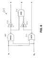
- FIG. 1 shows a partial block diagram of apparatus 101 including a cyclic DAC 100 , according to an embodiment of the invention.
- Apparatus 101 can include or be included in audio, video, telecommunication, networking, imaging, sensor, or other systems.
- DAC 100 receives a N bits digital input code b 0 through b N-1 (b N-1 , . . . , b 2 , b 1 , b 0 ) from a digital information unit 102 and generates an analog output voltage Vout (or VDAC).
- An analog information unit 104 receives voltage Vout from DAC 100 for further processing.
- DAC 100 operates as a cyclic digital to analog converter. In operation, DAC 100 initially sets (or resets) output voltage Vout to an initial value, e.g., zero. Then, DAC 100 successively applies a reference output voltage to output voltage Vout to obtain a final value of Vout that represents an analog voltage value corresponding to the data input code. DAC 100 selects from among three reference voltage ⁇ Vref, 0 , and +Vref (e.g., Vref) and applies the selected reference voltage to output voltage Vout. Each selection of the reference voltage to be applied is based on the value of one of the bits of the digit input code. The value of one of the three reference values can be zero, as shown in FIG. 1 . The following description shows details of the operation of DAC 100 .
- DAC 100 successively updates each value of output voltage Vout based on a recursive equation (1) below, until a final value of Vout is obtained.
- Vout j Vout j - 1 + f i ⁇ Vref 2 ( equation ⁇ ⁇ 1 )
- Integer f i is a function of b i .
- DAC 100 can start the conversion with the least significant bit (LSB) applied first or with the most significant bit (MSB) applied first.
- LSB applied first technique a first value of voltage Vout is generated based on the LSB of the digital input code.
- MSB applied first technique a first value of voltage Vout is generated based on the MSB of the digital input code.
- digital input code b N-1 , . . . , b 2 , b 1 , b 0 the LSB is b 0
- the MSB is b N-1 .
- This example uses the LSB applied first technique in which a first value of Vout is generated corresponding to the value of bit b 0 . From equation (1), the value of output voltage Vout corresponding to each bit of the digital input code is generated as followed.
- Vout N-1 Vout 2 , as shown above.
- the output voltage of DAC 100 is generated based on equation (4) below.
- the above equation (4) shows the output voltage of DAC 100 when an LSB applied first technique is used.
- the final result of the output voltage Vout N-1 would be the same as Vout N-1 in the case of the LSB applied first technique.
- f i can have three possible values: ⁇ 1, 0, and +1.
- the value of output voltage Vout before a division by two, can decrease (e.g., by subtracting a reference voltage Vref), increase (e.g., by adding a reference voltage Vref), or remain unchanged (adding or subtracting zero).
- Vout j-1 represents the output voltage value calculated by DAC 100 at step j ⁇ 1, which is a step immediately before step j, also called a previous step.
- the value of Vout j can be the previous output voltage value Vout j-1 minus a reference voltage Vref and then divided by two (equation 5), Vout j-1 plus a reference voltage Vref and then divided by two (equation 7), or Vout j-1 plus zero and then divided by two (equation 6).
- the above description relates to a general recursive step to obtain Vout j during a particular step.
- the reference voltage Vref is normalized, meaning that +Vref is +1 and ⁇ Vref is ⁇ 1.
- the range of the output voltage is between ⁇ 1 and +1 or ⁇ Vref ⁇ Vout ⁇ +Vref.
- the values of f 0 , f 1 , and f 2 are calculated based on equation (2) and (3) above.
- Table 2 below shows step-by-step details of Vout generated by DAC 100 for all eight possible combinations of digital input code b 2 , b 1 , b 0 based on the mapping of Table 1.
- Vout j f i desired (Vout j-1 + f i ⁇ Vref)/2 i bi binary decimal “ ⁇ 1/0/+1” analog j
- Vout j [step] reset ⁇ 1 0.000 0.000 0 b0 0 0 ⁇ 1 ⁇ 0.125 0 ⁇ 0.500 0.500 1 b1 0 0 ⁇ 1 ⁇ 0.250 1 ⁇ 0.750 0.250 2 b2 0 0 ⁇ 1 ⁇ 0.500 2 ⁇ 0.875 0.125 b ⁇ 2:0> Digital value 0 max step Analog value (V) ⁇ 0.875 ⁇ 0.875 0.500 reset ⁇ 1 0.000 0.000 0 b0 1 1 ⁇ 1 ⁇ 0.125 0 ⁇ 0.500 0.500 1 b1 0 0 0 0.000 1 ⁇ 0.250 0.250 2 b2 0 0 ⁇ 1 ⁇ 0.500 2 ⁇ 0.625 0.375 b ⁇ 2:0> Digital value 1 max step Analog value (V) ⁇ 0.625 ⁇ 0.6
- a conversion of each combination of b 2 , b 1 , b 0 includes four steps j, shown in column j as four steps labeled ⁇ 1, 0, 1, and 2.
- Table 2 also shows other values of Vout at other steps (0, 1, 2) j for each combination of b 2 , b 1 , b 0 .
- the values of Vout are 0.500, 0.750, and 0.375, with 0.375 being the final value of Vout.
- the values of Vout are 0.500, ⁇ 0.250, and ⁇ 0.125, with ⁇ 0.125 being the final value of Vout.
- the algorithm described herein can also be applied to a DAC of more than three bits.
- DAC 100 of FIG. 1 In comparison to some conventional digital to analog converters (DACs), DAC 100 of FIG. 1 generally can have a smaller length of the path for output voltage Vout.
- the time for DAC 100 to reach a final value (Vout N-1 ) of the output voltage can be smaller than that of conventional DACs, for the same accuracy. Therefore, DAC 100 can also be faster than conventional DACs.
- FIG. 4 shows a partial block diagram of a DAC 400 , according to an embodiment of the invention.
- DAC 400 includes an analog reference voltage generator 401 , a digital phase generator 402 , a input data storage 403 , an input data encoder 404 , an N-bit parallel to serial converter 405 , a conversion unit 406 , and a sample and hold output unit 407 .
- Analog reference voltage generator 401 generate reference voltages (signals) VRP, VRN, and VCM that are used during a conversion of a digital input code b 0 , b 1 , and b 2 through b N-1 received at data input storage 403 .
- Reference voltages VRP, VRN, and VCM are corresponding respectively to reference voltages +Vref, ⁇ Vref, and 0 described above.
- Digital phase generator 402 receives a clock signal CLK, a signal SOC (start of conversion) to start a conversion of a digital input code, and a reset signal RST to reset DAC 400 before conversion of a first bit of a digital input code.
- DAC 400 provides a signal EOC (end of cycle) upon completion of a conversion of a digital input code.
- Digital phase generator 402 also generates signals P 0 , P 1 , P 2 , and time ⁇ N ⁇ 1:0> (i.e., time ⁇ 0 > through time ⁇ N ⁇ 1>) in a regular sequence, and uses these signals during a conversion of a digital input code, as described in more details below with reference to FIG. 5 through FIG. 9 .
- Input data encoder 404 in FIG. 4 receives the N-bit digital input code b 0 , b 1 , and b 2 through b N-1 in parallel and generates a first parallel N bits A ⁇ N ⁇ 1:0> (i.e., A 0 through A N-1 ) on a first set of N lines; a second parallel N bits B ⁇ N ⁇ 1:0> (i.e., B 0 through B N-1 ) on a second set of N lines; and a third parallel N bits C ⁇ N ⁇ 1:0> (i.e., C 0 through C N-1 ) on a third set of N lines.
- Parallel to serial converter 405 converts the parallel N bits A ⁇ N ⁇ 1:0> into one serial bit A S , the parallel N bits B ⁇ N ⁇ 1:0> into one serial bit B S , and the parallel N bits C ⁇ N ⁇ 1:0> into one serial bit C S . As shown in FIG. 4 , each of the serial bits A S , B S , C S , is transferred on a single line from parallel to serial converter 405 to conversion unit 406 .
- Conversion unit 406 receives the 3 serial bits A S , B S , and C S based on timing of time time ⁇ N ⁇ 1:0> as follows.
- a S A 0 ⁇ time ⁇ 0>+ A 1 ⁇ time ⁇ 1 >+ . . . +A i ⁇ time ⁇ i>+ . . . +A N-1 ⁇ time ⁇ N ⁇ 1>
- B S B 0 ⁇ time ⁇ 0>+ B 1 ⁇ time ⁇ 1 >+ . . . +B i ⁇ time ⁇ i>+ . . . +B N-1 ⁇ time ⁇ N ⁇ 1>
- C S C 0 ⁇ time ⁇ 0>+ C 1 ⁇ time ⁇ 1>+ . . . +C i ⁇ time ⁇ i>+ . . . +C N-1 ⁇ time ⁇ N ⁇ 1>
- a S A N-1 ⁇ time ⁇ 0 >+A N-2 ⁇ time ⁇ 1 >+ . . . +A N-1-i ⁇ time ⁇ i>+ . . . +A 0 ⁇ time ⁇ N ⁇ 1>
- B S B N-1 ⁇ time ⁇ 0 >+B N-2 ⁇ time ⁇ 1 >+ . . . +B N-1-i ⁇ time ⁇ i>+ . . . +B 0 ⁇ time ⁇ N ⁇ 1>
- C S C N-1 ⁇ time ⁇ 0 >+C N-2 ⁇ time ⁇ 1 >+ . . . +C N-1-i ⁇ time ⁇ i>+ . . . +C 0 ⁇ time ⁇ N ⁇ 1>
- Conversion unit 406 also receives signals P 0 , P 1 , P 2 and analog reference voltages (signals) VRP, VCM, VRN, and generates output voltage Vout in response to bits A S , B S , and C S .
- FIG. 5 shows a block diagram of an encoder 504 , according to an embodiment of the invention.
- Encoder 504 can be substituted for input data encoder 404 of FIG. 4 .
- encoder 504 includes N identical encoder elements numbered from 0 to N ⁇ 1.
- Encoder 504 receives digital input code b N-1 , . . . , b 2 , b 1 , b 0 (or b ⁇ N ⁇ 1:0>) and output three parallel N-bit digital bits (or control bits) A ⁇ N ⁇ 1:0>, B ⁇ N ⁇ 1:0>, and C ⁇ N ⁇ 1:0>.
- FIG. 1 digital input code
- N 12 bits and the encoding is independent from the technique (LSB or MSB applied first) used to generate the output voltage.
- FIG. 6 shows a schematic diagram of an encoder element 605 , according to an embodiment of the invention.
- Encoder element 605 includes two digital input b i and b N-1 and three digital output a, b, and c.
- Encoder element 605 includes a combination of five digital gates including a NAND gate 610 , a NOR gate 612 , an AND gate 614 , and inverters 616 and 618 .
- FIG. 6 shows an example of encoder element 605 .
- Other implementation can be used to generate output a, b, and c.
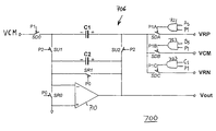
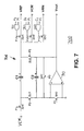
- FIG. 7 shows a partial block diagram of a DAC 700 having a conversion unit 706 , according to an embodiment of the invention.
- Conversion unit 706 can be substituted for conversion unit 406 of DAC 400 of FIG. 4 .
- Conversion unit 706 is a single-ended version of a digital to analog conversion unit used to generate a single-ended analog output voltage Vout.
- a fully differential conversion unit to generate a differential output voltage can also be implemented, such as the one shown in FIG. 9 .
- DAC 700 includes three analog reference voltages VRP, VCM, and VRN, which can be used to provide reference voltages such as +Vref, 0 , and ⁇ Vref described above with reference to FIG. 1 through FIG. 6 .
- Reference voltage VCM has a value equal to the average of the values of reference voltages VRP and VRN.
- DAC 700 also includes three digital inputs A S , B S , and C S containing information of the serial input code at corresponding allocated time slots.
- a S , B S , and C S correspond to A ⁇ N ⁇ 1:0>, B ⁇ N ⁇ 1:0>, and C ⁇ N ⁇ 1:0>, respectively, described above with reference to FIG. 4 and FIG. 5 .
- DAC 700 also includes three signals P 0 , P 1 , P 2 containing information of a reset phase (P 0 ), a sampling phase (P 1 ), and an analog update phase (P 2 ).
- DAC 700 also includes an amplifier 710 and a capacitor network including capacitors C 1 and C 2 .
- Amplifier 710 is a single-ended operational amplifier. However, a fully differential operational amplifier can be used in the differential version of conversion unit 706 .
- Capacitors C 1 and C 2 have the same capacitance value C.
- DAC 700 also includes switching circuitry having switches SD 0 , SDA, SDB, SDC, SU 1 , SU 2 , SR 0 , and SR 1 . Switches SDA, SDB, and SDC are controlled by control signals P 1 A, P 1 B, and P 1 C, respectively.
- the switches shown in FIG. 7 may be implemented using any suitable circuit element(s).
- one or more switches are implemented using isolated gate transistors such as metal oxide semiconductor field effect transistors (MOSFET).
- MOSFET metal oxide semiconductor field effect transistors
- complementary MOSFETs are coupled in parallel to form pass gates.
- an n-channel MOSFET may be coupled in parallel with a p-channel MOSFET as a transistor pass gate to implement one or more switches in FIG. 7 .
- gates 721 , 722 , and 723 can include logical AND gates to generate signals P 1 A, P 1 B, and P 1 C.
- DAC 700 uses switches SR 0 and SR 1 to reset conversion unit 706 , for example, to set output voltage Vout initially at zero.
- DAC 700 uses switches SD 0 , SDA, SDB, and SDC to apply reference voltages to the capacitor C 1 .
- DAC 700 uses switches SU 1 and SU 2 to update analog output voltage Vout during a conversion. The operation of DAC 700 is described below with reference to both FIG. 7 and FIG. 8 .
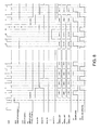
- FIG. 8 is an example timing diagram for DAC 700 of FIG. 7 , according to an embodiment of the invention.
- Signal CLK is the input clock.
- the number 1, 2, 3, 4, and 5 through 25 next to the waveform of signal CLK correspond to the periods of the CLK signal.
- the SOC goes high again at the start of a next conversion.
- EOC is the end of cycle signal generated when the conversion is completed.
- EOC lower level
- the SOC signal can go to a high level at the same time the EOC is high, in order to restart another conversion when the previous one has completed.
- P 0 is for the beginning of the cycle.
- Time ⁇ 0 >, time ⁇ 1 >, and time ⁇ 2 > through time ⁇ N ⁇ 1> are periods of time corresponding to the bits being treated during the conversion cycle.
- the conversion cycle is based on the LSB first technique, as shown by bits A ⁇ 0 >, B ⁇ 0 >, and C ⁇ 0 > being treated at period number 1 of the CLK signal.
- Serial data A S , B S , and C S are changed on the high level of the time ⁇ 0 > through time ⁇ N ⁇ 1>.
- a input data encoder (such as input data encoder 404 of FIG. 4 ) of DAC 700 produces data A S , B S , and C S , such that A S , B S , and C S are stable when P 1 is high for reliable conversion.
- Signal P 1 is used for sampling the reference voltages (VRP, VCM, VRN) during the conversion.
- Signal P 2 is used for updating the value of analog output voltage Vout.
- signals P 1 and P 2 are alternately asserted.
- the time period during which P 1 is asserted is referred to herein as “phase one” for a particular data bit.
- the time period during which P 2 is asserted is referred to herein as “phase two” for the same data bit.
- phases one and two do not overlap, such that they cannot both be high at the same time. For example, the switches in FIG. 7 that are turned on (closed) during phase one are turned off (opened) before the phase two switches close during phase two.
- phase two switches are turned off prior to the phase one switches turning on.
- the width of signals P 1 and P 2 when they are high can be substantially equal to the period of the CLK signal (Tclk), such that the non overlap delay is negligible relative to Tclk.
- the total number of periods of the CLK signal used in a conversion (T DAC ) is calculated as follows.
- Resetting conversion unit 706 can be performed in one period Tclk of the CLK signal at the beginning of the conversion, which is the time between the rising edge of the P 0 signal and the first rising edge of the P 1 signal at period number 1 of the CLK signal.
- T DAC 25. If the CLK signal has as frequency of 50 MHz (megahertz) used in conversion unit 706 , then DAC 700 will produce a data rate of 2 Msps (Million of samples per second). The operation of DAC 700 based on the timing of FIG. 8 is described below.
- Capacitor C 1 is charged as follows.
- the update of the output voltage Vout is performed by letting the capacitor C 1 and C 2 share their respective charges without loading input nodes (+ and ⁇ ) of amplifier 710 for the charge sharing.
- DAC 700 can be relatively insensitive to the amplifier bandwidth of amplifier 710 .
- the capacitance values of capacitors C 1 and C 2 can be relatively large without affecting the speed of the DAC 700 . Errors due to mismatch in coefficient values of capacitors C 1 and C 2 can also be minimized.
- Voutdiff analog output voltage
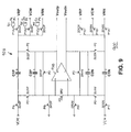
- DAC 900 includes reference voltages VRP, VCM, and VRN, an operational amplifier 910 , a capacitor network including capacitors C 1 P, C 2 P, C 1 N, and C 2 N, and a switching circuitry including switches SD 0 P, SDAP, SDBP, SDCP, SU 1 P, SU 2 P, SR 1 P, SR 2 P, SD 0 N, SDAN, SDBN, SDCN, SU 1 N, SU 2 N, SR 1 N, SR 2 N, and SR 0 . These switches are controlled by signals P 1 A, P 1 B, and P 1 C, as shown in FIG. 9 .
- DAC 900 also includes gates 921 , 922 , and 923 to generate signals P 1 A, P 1 B, and P 1 C based on signal P 1 and signals A S , B S , and C S .
- DAC 900 The operation of DAC 900 is similar to the operation of DAC 700 of FIG. 7 .
- a zero voltage is also stored across capacitors C 2 P and C 2 N which are shorted by switches SR 1 P and SR 1 N being turned on.
- Capacitors C 1 P and C 1 N are charged as follows.
- capacitor C 1 P is connected in parallel with capacitor C 2 P between the inverted ( ⁇ ) input node and the output node (+) of amplifier 910 .
- Capacitor C 1 N is connected in parallel with capacitor C 2 N between the noninverted (+) input node and the output node ( ⁇ ) of amplifier 910 .
- ⁇ Voutdiff j Voutp j - Voutn j
- the amplitude of analog output voltage Voutdiff of DAC 900 of FIG. 9 is twice the amplitude of analog output voltage Vout of DAC 700 of FIG. 7 because Voutdiff associated with FIG. 9 is differential whereas Vout associated with FIG. 7 is single-ended. Therefore, in applications where the output dynamic range of the DAC is a concern, DAC 900 can be more applicable than DAC 700 .
- One or more embodiments described herein include apparatus and methods having an amplifier, a capacitor network coupled to the amplifier, and switching circuitry coupled to the amplifier and the capacitor network.
- the switching circuit is configured to successively apply a selected reference voltage selected from among a first reference voltage, a second reference voltage, and a third reference voltage to the capacitor network in response to a digital input code to generate an output voltage.
- Other embodiments, including additional apparatus and methods, are described above with reference to FIG. 1 through FIG. 9 .
- apparatus 101 such as apparatus 101 , DAC 400 , DAC 700 , and DAC 900 , are intended to provide a general understanding of the structure of various embodiments and not a complete description of all the elements and features of the apparatus that might make use of the structures described herein.
- modules can include hardware circuitry, single and/or multi-processor circuits, memory circuits, software program modules and objects and/or firmware, and combinations thereof, as desired by the architect of the apparatus (e.g., apparatus 101 , DAC 400 , DAC 700 , and DAC 900 ), and as appropriate for particular implementations of various embodiments.
- modules may be included in a system operation simulation package, such as a software electrical signal simulation package, a power usage and distribution simulation package, a capacitance-inductance simulation package, a power/heat dissipation simulation package, a signal transmission-reception simulation package, and/or a combination of software and hardware used to operate or simulate the operation of various potential embodiments.
- a system operation simulation package such as a software electrical signal simulation package, a power usage and distribution simulation package, a capacitance-inductance simulation package, a power/heat dissipation simulation package, a signal transmission-reception simulation package, and/or a combination of software and hardware used to operate or simulate the operation of various potential embodiments.
- the apparatus of various embodiments includes or can be included in electronic circuitry used in high-speed computers, communication and signal processing circuitry, memory modules, portable memory storage devices (e.g., thumb drives), single or multi-processor modules, single or multiple embedded processors, multi-core processors, data switches, and application-specific modules including multilayer and multi-chip modules.
- Such apparatus may further be included as sub-components within a variety of electronic systems such as televisions, memory cellular telephones, personal computers (e.g., laptop computers, desktop computers, handheld computers, tablet computers, etc.), workstations, radios, video players, audio players (e.g., MP3 (Motion Picture Experts Group, Audio Layer 3) players), vehicles, medical devices (e.g., heart monitor, blood pressure monitor, etc.), set top boxes, and others.
- televisions e.g., laptop computers, desktop computers, handheld computers, tablet computers, etc.
- workstations e.g., radios, video players, audio players (e.g., MP3 (Motion Picture Experts Group, Audio Layer 3) players), vehicles, medical devices (e.g., heart monitor, blood pressure monitor, etc.), set top boxes, and others.
- MP3 Motion Picture Experts Group, Audio Layer 3
Abstract
Description
f 0=2b N-1−1 (equation 2)
f i =b N-1−1+b i-1 (equation 3)
f i =b N-1−1+b i-1=−1 if b N-1=0 and b i-1=0
f i =b N-1−1+b i-1=0 if b N-1=0 and b i-1=1 (or if b N-1=1 and b i-1=0)
f i =b N-1−1+b i-1=+1 if b N-1=1 and b i-1=1
| TABLE 1 | ||
| b2, b1, b0 | f2, f1, f0 | Output Voltage (Vout) |
| decimal | binary | equation (2) and (3) | normalized |
| 0 | 000 | −1 −1 −1 | −7/8 |
| 1 | 001 | −1 0 −1 | −5/8 |
| 2 | 010 | 0 −1 −1 | −3/8 |
| 3 | 011 | 0 0 −1 | −1/8 |
| 4 | 100 | 0 0 +1 | +1/8 |
| 5 | 101 | 0 +1 +1 | +3/8 |
| 6 | 110 | +1 0 +1 | +5/8 |
| 7 | 111 | +1 +1 +1 | +7/8 |
| TABLE 2 | ||||
| Voutj = | ||||
| fi | desired | (Voutj-1 + fi · Vref)/2 | ||
| i | bi | binary | decimal | “−1/0/+1” | analog | j | Voutj | [step] |
| reset | −1 | 0.000 | 0.000 | |||||
| 0 | b0 | 0 | 0 | −1 | −0.125 | 0 | −0.500 | 0.500 |
| 1 | b1 | 0 | 0 | −1 | −0.250 | 1 | −0.750 | 0.250 |
| 2 | b2 | 0 | 0 | −1 | −0.500 | 2 | −0.875 | 0.125 |
| b<2:0> | Digital value | 0 | max step | |||||
| Analog value (V) | −0.875 | −0.875 | 0.500 | |||||
| reset | −1 | 0.000 | 0.000 | |||||
| 0 | b0 | 1 | 1 | −1 | −0.125 | 0 | −0.500 | 0.500 |
| 1 | b1 | 0 | 0 | 0 | 0.000 | 1 | −0.250 | 0.250 |
| 2 | b2 | 0 | 0 | −1 | −0.500 | 2 | −0.625 | 0.375 |
| b<2:0> | Digital value | 1 | max step | |||||
| Analog value (V) | −0.625 | −0.625 | 0.500 | |||||
| reset | −1 | 0.000 | 0.000 | |||||
| 0 | b0 | 0 | 0 | −1 | −0.125 | 0 | −0.500 | 0.500 |
| 1 | b1 | 1 | 2 | −1 | −0.250 | 1 | −0.750 | 0.250 |
| 2 | b2 | 0 | 0 | 0 | 0.000 | 2 | −0.375 | 0.375 |
| b<2:0> | Digital value | 2 | max step | |||||
| Analog value (V) | −0.375 | −0.375 | 0.500 | |||||
| reset | −1 | 0.000 | 0.000 | |||||
| 0 | b0 | 1 | 1 | −1 | −0.125 | 0 | −0.500 | 0.500 |
| 1 | b1 | 1 | 2 | 0 | 0.000 | 1 | −0.250 | 0.250 |
| 2 | b2 | 0 | 0 | 0 | 0.000 | 2 | −0.125 | 0.125 |
| b<2:0> | Digital value | 3 | max step | |||||
| Analog value (V) | −0.125 | −0.125 | 0.500 | |||||
| reset | −1 | 0.000 | 0.000 | |||||
| 0 | b0 | 0 | 0 | 1 | 0.125 | 0 | 0.500 | 0.500 |
| 1 | b1 | 0 | 0 | 0 | 0.000 | 1 | 0.250 | 0.250 |
| 2 | b2 | 1 | 4 | 0 | 0.000 | 2 | 0.125 | 0.125 |
| b<2:0> | Digital value | 4 | max step | |||||
| Analog value (V) | 0.125 | 0.125 | 0.500 | |||||
| reset | −1 | 0.000 | 0.000 | |||||
| 0 | b0 | 1 | 1 | 1 | 0.125 | 0 | 0.500 | 0.500 |
| 1 | b1 | 0 | 0 | 1 | 0.250 | 1 | 0.750 | 0.250 |
| 2 | b2 | 1 | 4 | 0 | 0.000 | 2 | 0.375 | 0.375 |
| b<2:0> | Digital value | 5 | max step | |||||
| Analog value (V) | 0.375 | 0.375 | 0.500 | |||||
| reset | −1 | 0.000 | 0.000 | |||||
| 0 | b0 | 0 | 0 | 1 | 0.125 | 0 | 0.500 | 0.500 |
| 1 | b1 | 1 | 2 | 0 | 0.000 | 1 | 0.250 | 0.250 |
| 2 | b2 | 1 | 4 | 1 | 0.500 | 2 | 0.625 | 0.375 |
| b<2:0> | Digital value | 6 | max step | |||||
| Analog value (V) | 0.625 | 0.625 | 0.500 | |||||
| reset | −1 | 0.000 | 0.000 | |||||
| 0 | b0 | 1 | 1 | 1 | 0.125 | 0 | 0.500 | 0.500 |
| 1 | b1 | 1 | 2 | 1 | 0.250 | 1 | 0.750 | 0.250 |
| 2 | b2 | 1 | 4 | 1 | 0.500 | 2 | 0.875 | 0.125 |
| b<2:0> | Digital value | 7 | max step | |||||
| Analog value (V) | 0.875 | 0.875 | 0.500 | |||||
A S =A0·time<0>+A1·time<1>+ . . . +A i·time<i>+ . . . +A N-1·time<N−1>
B S =B0·time<0>+B1·time<1>+ . . . +B i·time<i>+ . . . +B N-1·time<N−1>
C S =C0·time<0>+C1·time<1>+ . . . +Ci·time<i>+ . . . +C N-1·time<N−1>
A S =A N-1·time<0>+A N-2·time<1>+ . . . +A N-1-i·time<i>+ . . . +A0·time<N−1>
B S =B N-1·time<0>+B N-2·time<1>+ . . . +B N-1-i·time<i>+ . . . +B0·time<N−1>
C S =C N-1·time<0>+C N-2·time<1>+ . . . +C N-1-i·time<i>+ . . . +C0·time<N−1>
A i=1 when f i=+1 otherwise A i=0
B i=1 when f i=0 otherwise B i=0
C i=1 when f i=−1 otherwise C i=0
Table 3 is a truth table for
| TABLE 3 | ||||
| input | representation | output | ||
| code | b3 | b2 | b1 | b0 | f3 | f2 | f1 | f0 | A3 | A2 | A1 | A0 | B3 | B2 | B1 | B0 | C3 | C2 | C1 | C0 |
| 0 | 0 | 0 | 0 | 0 | −1 | −1 | −1 | −1 | 0 | 0 | 0 | 0 | 0 | 0 | 0 | 0 | 1 | 1 | 1 | 1 |
| 1 | 0 | 0 | 0 | 1 | −1 | −1 | 0 | −1 | 0 | 0 | 0 | 0 | 0 | 0 | 1 | 0 | 1 | 1 | 0 | 1 |
| 2 | 0 | 0 | 1 | 0 | −1 | 0 | −1 | −1 | 0 | 0 | 0 | 0 | 0 | 1 | 0 | 0 | 1 | 0 | 1 | 1 |
| 3 | 0 | 0 | 1 | 1 | −1 | 0 | 0 | −1 | 0 | 0 | 0 | 0 | 0 | 1 | 1 | 0 | 1 | 0 | 0 | 1 |
| 4 | 0 | 1 | 0 | 0 | 0 | −1 | −1 | −1 | 0 | 0 | 0 | 0 | 1 | 0 | 0 | 0 | 0 | 1 | 1 | 1 |
| 5 | 0 | 1 | 0 | 1 | 0 | −1 | 0 | −1 | 0 | 0 | 0 | 0 | 1 | 0 | 1 | 0 | 0 | 1 | 0 | 1 |
| 6 | 0 | 1 | 1 | 0 | 0 | 0 | −1 | −1 | 0 | 0 | 0 | 0 | 1 | 1 | 0 | 0 | 0 | 0 | 1 | 1 |
| 7 | 0 | 1 | 1 | 1 | 0 | 0 | 0 | −1 | 0 | 0 | 0 | 0 | 1 | 1 | 1 | 0 | 0 | 0 | 0 | 1 |
| 8 | 1 | 0 | 0 | 0 | 0 | 0 | 0 | +1 | 0 | 0 | 0 | 1 | 1 | 1 | 1 | 0 | 0 | 0 | 0 | 0 |
| 9 | 1 | 0 | 0 | 1 | 0 | 0 | +1 | +1 | 0 | 0 | 1 | 1 | 1 | 1 | 0 | 0 | 0 | 0 | 0 | 0 |
| 10 | 1 | 0 | 1 | 0 | 0 | +1 | 0 | +1 | 0 | 1 | 0 | 1 | 1 | 0 | 1 | 0 | 0 | 0 | 0 | 0 |
| 11 | 1 | 0 | 1 | 1 | 0 | +1 | +1 | +1 | 0 | 1 | 1 | 1 | 1 | 0 | 0 | 0 | 0 | 0 | 0 | 0 |
| 12 | 1 | 1 | 0 | 0 | +1 | 0 | 0 | +1 | 1 | 0 | 0 | 1 | 0 | 1 | 1 | 0 | 0 | 0 | 0 | 0 |
| 13 | 1 | 1 | 0 | 1 | +1 | 0 | +1 | +1 | 1 | 0 | 1 | 1 | 0 | 1 | 0 | 0 | 0 | 0 | 0 | 0 |
| 14 | 1 | 1 | 1 | 0 | +1 | +1 | 0 | +1 | 1 | 1 | 0 | 1 | 0 | 0 | 1 | 0 | 0 | 0 | 0 | 0 |
| 15 | 1 | 1 | 1 | 1 | +1 | +1 | +1 | +1 | 1 | 1 | 1 | 1 | 0 | 0 | 0 | 0 | 0 | 0 | 0 | 0 |
| output | note | ||
| a = bN−1 · bi | (AND) | ||
| b = bN−1 ⊕ bi | ⊕ is the XOR (exclusive | ||
| or) | |||
| c = | (NOR) | ||
The output (a,b,c) of
The truth table for
| TABLE 4 | ||
| input | output | |
| bN−1 | bi | a | | c | |
| 0 | 0 | 0 | 0 | 1 | |
| 0 | 1 | 0 | 1 | 0 | |
| 1 | 0 | 0 | 1 | 0 | |
| 1 | 1 | 1 | 0 | 0 | |
VRP−VCM=+Vref through switch SDA if A S=1
VCM−VCM=0 through switch SDB if B S=1
VRN−VCM=−Vref through switch SDC if C S=1
(at step j,P1=1), Voutj =Voutj-1
Thus the final output voltage is reached at the end of the last P2=1 time slot.
VRP−VCM=+Vref through switch SDAP if A S=1
VCM−VCM=0 through switch SDBP if B S=1
VRN−VCM=−Vref through switch SDCP if C S=1
VRN−VCM=−Vref through switch SDAN if A S=1
VCM−VCM=0 through switch SDBN if B S=1
VRP−VCM=+Vref through switch SDCN if C S=1
(at step j,P1=1), Voutp j =Voutp j-1
(at step j,P1=1), Voutn j =Voutn j-1
(at step j,P1=1), Voutdiffj =Voutdiffj-1
Claims (23)
Priority Applications (1)
| Application Number | Priority Date | Filing Date | Title |
|---|---|---|---|
| US12/436,620 US8223056B2 (en) | 2009-05-06 | 2009-05-06 | Cyclic digital to analog converter |
Applications Claiming Priority (1)
| Application Number | Priority Date | Filing Date | Title |
|---|---|---|---|
| US12/436,620 US8223056B2 (en) | 2009-05-06 | 2009-05-06 | Cyclic digital to analog converter |
Publications (2)
| Publication Number | Publication Date |
|---|---|
| US20100283651A1 US20100283651A1 (en) | 2010-11-11 |
| US8223056B2 true US8223056B2 (en) | 2012-07-17 |
Family
ID=43062046
Family Applications (1)
| Application Number | Title | Priority Date | Filing Date |
|---|---|---|---|
| US12/436,620 Active US8223056B2 (en) | 2009-05-06 | 2009-05-06 | Cyclic digital to analog converter |
Country Status (1)
| Country | Link |
|---|---|
| US (1) | US8223056B2 (en) |
Cited By (1)
| Publication number | Priority date | Publication date | Assignee | Title |
|---|---|---|---|---|
| US20110163901A1 (en) * | 2009-07-16 | 2011-07-07 | Microchip Technology Incorporated | 2-phase gain calibration and scaling scheme for switched capacitor sigma-delta modulator using a chopper voltage reference |
Families Citing this family (3)
| Publication number | Priority date | Publication date | Assignee | Title |
|---|---|---|---|---|
| US8223056B2 (en) * | 2009-05-06 | 2012-07-17 | Atmel Corporation | Cyclic digital to analog converter |
| KR101594866B1 (en) * | 2009-06-02 | 2016-02-26 | 엘에스산전 주식회사 | Apparatus and method for converting parallel digital data to serial digital data for a circuit breaker |
| TWI691170B (en) * | 2019-12-30 | 2020-04-11 | 新唐科技股份有限公司 | Wave generator and method for generating waveform |
Citations (18)
| Publication number | Priority date | Publication date | Assignee | Title |
|---|---|---|---|---|
| US4622536A (en) | 1984-09-28 | 1986-11-11 | Regents Of The University Of California | Ratio independent cyclic A/D and D/A conversion using a reciprocating reference approach |
| US4988900A (en) * | 1988-12-28 | 1991-01-29 | Sgs-Thomson Microelectronics S.A. | Analog signal waveform generator |
| US5821891A (en) * | 1996-12-26 | 1998-10-13 | Nokia Mobile Phones, Ltd. | Second order demodulator for sigma-delta digital to analog converter |
| US5892473A (en) * | 1996-06-24 | 1999-04-06 | Hyundai Electronics Industries Co., Ltd. | Switched capacitor digital-analog converter with a decreased harmonic distortion |
| US5923275A (en) * | 1997-10-22 | 1999-07-13 | National Semiconductor Corporation | Accurate charge-dividing digital-to-analog converter |
| US5990819A (en) | 1997-07-31 | 1999-11-23 | Asahi Kasei Microsystems Co., Ltd. | D/A converter and delta-sigma D/A converter |
| US6952176B2 (en) * | 2003-12-05 | 2005-10-04 | Wolfson Microelectronics Plc | Digital-to-analogue converter circuits |
| US7034737B1 (en) * | 2005-03-28 | 2006-04-25 | Faraday Technology Corp. | Switched capacitor circuits |
| US7061418B2 (en) * | 2004-01-03 | 2006-06-13 | Sharp Kabushiki Kaisha | Digital/analog converter, display driver and display |
| US7102557B1 (en) * | 2005-04-19 | 2006-09-05 | Wolfson Microelectronics Plc | Switched capacitor DAC |
| US7199743B2 (en) | 2004-12-29 | 2007-04-03 | Intel Corporation | Cyclic digital to analog converter |
| US7265705B1 (en) * | 2006-08-10 | 2007-09-04 | National Semiconductor Corporation | Opamp and capacitor sharing scheme for low-power pipeline ADC |
| US7436341B2 (en) * | 2005-11-29 | 2008-10-14 | Alpha Imaging Technology Corp. | Digital/analog converting apparatus and digital/analog converter thereof |
| US7443329B2 (en) * | 2005-09-08 | 2008-10-28 | Marvell World Trade Ltd. | Capacitive digital to analog and analog to digital converters |
| US7551113B2 (en) * | 2007-03-27 | 2009-06-23 | Samsung Electronics Co., Ltd. | Cyclic digital to analog converter in pipeline structure |
| US20090231176A1 (en) * | 2008-03-12 | 2009-09-17 | Sunplus Mmedia Inc. | Switched capacitor digital-to-analog converter |
| US7629917B2 (en) * | 2005-04-18 | 2009-12-08 | Digian Technology, Inc. | Integrator and cyclic AD converter using the same |
| US20100283651A1 (en) * | 2009-05-06 | 2010-11-11 | Atmel Corporation | Cyclic digital to analog converter |
-
2009
- 2009-05-06 US US12/436,620 patent/US8223056B2/en active Active
Patent Citations (18)
| Publication number | Priority date | Publication date | Assignee | Title |
|---|---|---|---|---|
| US4622536A (en) | 1984-09-28 | 1986-11-11 | Regents Of The University Of California | Ratio independent cyclic A/D and D/A conversion using a reciprocating reference approach |
| US4988900A (en) * | 1988-12-28 | 1991-01-29 | Sgs-Thomson Microelectronics S.A. | Analog signal waveform generator |
| US5892473A (en) * | 1996-06-24 | 1999-04-06 | Hyundai Electronics Industries Co., Ltd. | Switched capacitor digital-analog converter with a decreased harmonic distortion |
| US5821891A (en) * | 1996-12-26 | 1998-10-13 | Nokia Mobile Phones, Ltd. | Second order demodulator for sigma-delta digital to analog converter |
| US5990819A (en) | 1997-07-31 | 1999-11-23 | Asahi Kasei Microsystems Co., Ltd. | D/A converter and delta-sigma D/A converter |
| US5923275A (en) * | 1997-10-22 | 1999-07-13 | National Semiconductor Corporation | Accurate charge-dividing digital-to-analog converter |
| US6952176B2 (en) * | 2003-12-05 | 2005-10-04 | Wolfson Microelectronics Plc | Digital-to-analogue converter circuits |
| US7061418B2 (en) * | 2004-01-03 | 2006-06-13 | Sharp Kabushiki Kaisha | Digital/analog converter, display driver and display |
| US7199743B2 (en) | 2004-12-29 | 2007-04-03 | Intel Corporation | Cyclic digital to analog converter |
| US7034737B1 (en) * | 2005-03-28 | 2006-04-25 | Faraday Technology Corp. | Switched capacitor circuits |
| US7629917B2 (en) * | 2005-04-18 | 2009-12-08 | Digian Technology, Inc. | Integrator and cyclic AD converter using the same |
| US7102557B1 (en) * | 2005-04-19 | 2006-09-05 | Wolfson Microelectronics Plc | Switched capacitor DAC |
| US7443329B2 (en) * | 2005-09-08 | 2008-10-28 | Marvell World Trade Ltd. | Capacitive digital to analog and analog to digital converters |
| US7436341B2 (en) * | 2005-11-29 | 2008-10-14 | Alpha Imaging Technology Corp. | Digital/analog converting apparatus and digital/analog converter thereof |
| US7265705B1 (en) * | 2006-08-10 | 2007-09-04 | National Semiconductor Corporation | Opamp and capacitor sharing scheme for low-power pipeline ADC |
| US7551113B2 (en) * | 2007-03-27 | 2009-06-23 | Samsung Electronics Co., Ltd. | Cyclic digital to analog converter in pipeline structure |
| US20090231176A1 (en) * | 2008-03-12 | 2009-09-17 | Sunplus Mmedia Inc. | Switched capacitor digital-to-analog converter |
| US20100283651A1 (en) * | 2009-05-06 | 2010-11-11 | Atmel Corporation | Cyclic digital to analog converter |
Non-Patent Citations (2)
| Title |
|---|
| Debrunner, L. S, et al., "Defining canonical-signed-digit number systems as arithmetic codes", Conference Record of the Thirty-Sixth Asilomar Conference on Signals, Systems and Computers, vol. 2, (2002), 1593-1597. |
| Matsumoto, H., et al., "Switched-capacitor algorithmic digital-to-analog converters", IEEE Transactions on Circuits and Systems, 33(7), (Jul. 1986), 721-724. |
Cited By (2)
| Publication number | Priority date | Publication date | Assignee | Title |
|---|---|---|---|---|
| US20110163901A1 (en) * | 2009-07-16 | 2011-07-07 | Microchip Technology Incorporated | 2-phase gain calibration and scaling scheme for switched capacitor sigma-delta modulator using a chopper voltage reference |
| US8339299B2 (en) * | 2009-07-16 | 2012-12-25 | Microchip Technology Incorporated | 2-phase gain calibration and scaling scheme for switched capacitor sigma-delta modulator using a chopper voltage reference |
Also Published As
| Publication number | Publication date |
|---|---|
| US20100283651A1 (en) | 2010-11-11 |
Similar Documents
| Publication | Publication Date | Title |
|---|---|---|
| US9859911B1 (en) | Successive approximation register analog-to-digital converter and analog-to-digital signal conversion method thereof | |
| US10103742B1 (en) | Multi-stage hybrid analog-to-digital converter | |
| US9094030B2 (en) | Successive approximation analog to digital converter and method of analog to digital conversion | |
| JP3281621B2 (en) | High precision DA conversion circuit | |
| US11640196B2 (en) | Unit element for performing multiply-accumulate operations | |
| US9432046B1 (en) | Successive approximation analog-to-digital converter | |
| US7425913B2 (en) | Bit-adjacency capacitor-switched DAC, method, driver and display device | |
| US8223056B2 (en) | Cyclic digital to analog converter | |
| JPS6161578B2 (en) | ||
| US7173557B2 (en) | Analog/digital converter | |
| US10211847B1 (en) | Successive approximation register analog-to-digital converter and method for operating the same | |
| CN109644002B (en) | Scalable random successive approximation register analog-to-digital converter | |
| US9553602B1 (en) | Methods and systems for analog-to-digital conversion (ADC) using an ultra small capacitor array with full range and sub-range modes | |
| JP6970597B2 (en) | Latched comparator | |
| US8860598B2 (en) | Bit error rate timer for a dynamic latch | |
| Arafa et al. | Successive approximation register analog-to-digital converter (SAR ADC) for biomedical applications | |
| Yeh et al. | A novel flash analog-to-digital converter | |
| US11764801B2 (en) | Computing-in-memory circuit | |
| US10411726B2 (en) | Quantizer including capacitors and operating method of quantizer | |
| JPH0212416B2 (en) | ||
| US11133816B1 (en) | Analog-digital converter and semiconductor memory device having the same | |
| US20090224951A1 (en) | Cyclic pipeline analog-to-digital converter | |
| KR101725833B1 (en) | Ten bit successive approximation register analog to digital converter | |
| Jensen | Configurable multiple value encoders using semi floating-gate | |
| Jensen et al. | Dual data-rate cyclic d/a converter using semi floating-gate devices |
Legal Events
| Date | Code | Title | Description |
|---|---|---|---|
| AS | Assignment |
Owner name: ATMEL CORPORATION, CALIFORNIA Free format text: ASSIGNMENT OF ASSIGNORS INTEREST;ASSIGNORS:DURA, RENAUD;CARREIRA, JOAO PEDRO;FIEVET, SEBASTIEN;REEL/FRAME:023894/0840 Effective date: 20090506 |
|
| AS | Assignment |
Owner name: ATMEL CORPORATION, CALIFORNIA Free format text: ASSIGNMENT OF ASSIGNORS INTEREST;ASSIGNORS:DURA, RENAUD;CARREIRA, JOAO PEDRO;FIEVET, SEBASTIEN;REEL/FRAME:026243/0357 Effective date: 20090506 |
|
| STCF | Information on status: patent grant |
Free format text: PATENTED CASE |
|
| CC | Certificate of correction | ||
| AS | Assignment |
Owner name: MORGAN STANLEY SENIOR FUNDING, INC. AS ADMINISTRATIVE AGENT, NEW YORK Free format text: PATENT SECURITY AGREEMENT;ASSIGNOR:ATMEL CORPORATION;REEL/FRAME:031912/0173 Effective date: 20131206 Owner name: MORGAN STANLEY SENIOR FUNDING, INC. AS ADMINISTRAT Free format text: PATENT SECURITY AGREEMENT;ASSIGNOR:ATMEL CORPORATION;REEL/FRAME:031912/0173 Effective date: 20131206 |
|
| FPAY | Fee payment |
Year of fee payment: 4 |
|
| AS | Assignment |
Owner name: ATMEL CORPORATION, CALIFORNIA Free format text: TERMINATION AND RELEASE OF SECURITY INTEREST IN PATENT COLLATERAL;ASSIGNOR:MORGAN STANLEY SENIOR FUNDING, INC.;REEL/FRAME:038376/0001 Effective date: 20160404 |
|
| AS | Assignment |
Owner name: JPMORGAN CHASE BANK, N.A., AS ADMINISTRATIVE AGENT, ILLINOIS Free format text: SECURITY INTEREST;ASSIGNOR:ATMEL CORPORATION;REEL/FRAME:041715/0747 Effective date: 20170208 Owner name: JPMORGAN CHASE BANK, N.A., AS ADMINISTRATIVE AGENT Free format text: SECURITY INTEREST;ASSIGNOR:ATMEL CORPORATION;REEL/FRAME:041715/0747 Effective date: 20170208 |
|
| AS | Assignment |
Owner name: JPMORGAN CHASE BANK, N.A., AS ADMINISTRATIVE AGENT, ILLINOIS Free format text: SECURITY INTEREST;ASSIGNORS:MICROCHIP TECHNOLOGY INCORPORATED;SILICON STORAGE TECHNOLOGY, INC.;ATMEL CORPORATION;AND OTHERS;REEL/FRAME:046426/0001 Effective date: 20180529 Owner name: JPMORGAN CHASE BANK, N.A., AS ADMINISTRATIVE AGENT Free format text: SECURITY INTEREST;ASSIGNORS:MICROCHIP TECHNOLOGY INCORPORATED;SILICON STORAGE TECHNOLOGY, INC.;ATMEL CORPORATION;AND OTHERS;REEL/FRAME:046426/0001 Effective date: 20180529 |
|
| AS | Assignment |
Owner name: WELLS FARGO BANK, NATIONAL ASSOCIATION, AS NOTES COLLATERAL AGENT, CALIFORNIA Free format text: SECURITY INTEREST;ASSIGNORS:MICROCHIP TECHNOLOGY INCORPORATED;SILICON STORAGE TECHNOLOGY, INC.;ATMEL CORPORATION;AND OTHERS;REEL/FRAME:047103/0206 Effective date: 20180914 Owner name: WELLS FARGO BANK, NATIONAL ASSOCIATION, AS NOTES C Free format text: SECURITY INTEREST;ASSIGNORS:MICROCHIP TECHNOLOGY INCORPORATED;SILICON STORAGE TECHNOLOGY, INC.;ATMEL CORPORATION;AND OTHERS;REEL/FRAME:047103/0206 Effective date: 20180914 |
|
| MAFP | Maintenance fee payment |
Free format text: PAYMENT OF MAINTENANCE FEE, 8TH YEAR, LARGE ENTITY (ORIGINAL EVENT CODE: M1552); ENTITY STATUS OF PATENT OWNER: LARGE ENTITY Year of fee payment: 8 |
|
| AS | Assignment |
Owner name: MICROCHIP TECHNOLOGY INCORPORATED, ARIZONA Free format text: RELEASE BY SECURED PARTY;ASSIGNOR:JPMORGAN CHASE BANK, N.A., AS ADMINISTRATIVE AGENT;REEL/FRAME:051398/0809 Effective date: 20191220 Owner name: ATMEL CORPORATION, ARIZONA Free format text: RELEASE BY SECURED PARTY;ASSIGNOR:WELLS FARGO BANK, NATIONAL ASSOCIATION, AS NOTES COLLATERAL AGENT;REEL/FRAME:051398/0827 Effective date: 20191220 Owner name: MICROCHIP TECHNOLOGY INCORPORATED, ARIZONA Free format text: RELEASE BY SECURED PARTY;ASSIGNOR:WELLS FARGO BANK, NATIONAL ASSOCIATION, AS NOTES COLLATERAL AGENT;REEL/FRAME:051398/0827 Effective date: 20191220 Owner name: ATMEL CORPORATION, ARIZONA Free format text: RELEASE BY SECURED PARTY;ASSIGNOR:JPMORGAN CHASE BANK, N.A., AS ADMINISTRATIVE AGENT;REEL/FRAME:051398/0809 Effective date: 20191220 |
|
| AS | Assignment |
Owner name: SONRAI MEMORY LIMITED, IRELAND Free format text: ASSIGNMENT OF ASSIGNORS INTEREST;ASSIGNORS:MICROCHIP TECHNOLOGY INC.;ATMEL CORPORATION;MICROSEMI CORPORATION;REEL/FRAME:051799/0956 Effective date: 20200203 |
|
| AS | Assignment |
Owner name: MICROSEMI STORAGE SOLUTIONS, INC., ARIZONA Free format text: RELEASE BY SECURED PARTY;ASSIGNOR:JPMORGAN CHASE BANK, N.A., AS ADMINISTRATIVE AGENT;REEL/FRAME:059333/0222 Effective date: 20220218 Owner name: MICROSEMI CORPORATION, ARIZONA Free format text: RELEASE BY SECURED PARTY;ASSIGNOR:JPMORGAN CHASE BANK, N.A., AS ADMINISTRATIVE AGENT;REEL/FRAME:059333/0222 Effective date: 20220218 Owner name: ATMEL CORPORATION, ARIZONA Free format text: RELEASE BY SECURED PARTY;ASSIGNOR:JPMORGAN CHASE BANK, N.A., AS ADMINISTRATIVE AGENT;REEL/FRAME:059333/0222 Effective date: 20220218 Owner name: SILICON STORAGE TECHNOLOGY, INC., ARIZONA Free format text: RELEASE BY SECURED PARTY;ASSIGNOR:JPMORGAN CHASE BANK, N.A., AS ADMINISTRATIVE AGENT;REEL/FRAME:059333/0222 Effective date: 20220218 Owner name: MICROCHIP TECHNOLOGY INCORPORATED, ARIZONA Free format text: RELEASE BY SECURED PARTY;ASSIGNOR:JPMORGAN CHASE BANK, N.A., AS ADMINISTRATIVE AGENT;REEL/FRAME:059333/0222 Effective date: 20220218 |
|
| AS | Assignment |
Owner name: ATMEL CORPORATION, ARIZONA Free format text: RELEASE BY SECURED PARTY;ASSIGNOR:JPMORGAN CHASE BANK, N.A., AS ADMINISTRATIVE AGENT;REEL/FRAME:059262/0105 Effective date: 20220218 |
|
| AS | Assignment |
Owner name: MICROSEMI STORAGE SOLUTIONS, INC., ARIZONA Free format text: RELEASE BY SECURED PARTY;ASSIGNOR:WELLS FARGO BANK, NATIONAL ASSOCIATION, AS NOTES COLLATERAL AGENT;REEL/FRAME:059358/0001 Effective date: 20220228 Owner name: MICROSEMI CORPORATION, ARIZONA Free format text: RELEASE BY SECURED PARTY;ASSIGNOR:WELLS FARGO BANK, NATIONAL ASSOCIATION, AS NOTES COLLATERAL AGENT;REEL/FRAME:059358/0001 Effective date: 20220228 Owner name: ATMEL CORPORATION, ARIZONA Free format text: RELEASE BY SECURED PARTY;ASSIGNOR:WELLS FARGO BANK, NATIONAL ASSOCIATION, AS NOTES COLLATERAL AGENT;REEL/FRAME:059358/0001 Effective date: 20220228 Owner name: SILICON STORAGE TECHNOLOGY, INC., ARIZONA Free format text: RELEASE BY SECURED PARTY;ASSIGNOR:WELLS FARGO BANK, NATIONAL ASSOCIATION, AS NOTES COLLATERAL AGENT;REEL/FRAME:059358/0001 Effective date: 20220228 Owner name: MICROCHIP TECHNOLOGY INCORPORATED, ARIZONA Free format text: RELEASE BY SECURED PARTY;ASSIGNOR:WELLS FARGO BANK, NATIONAL ASSOCIATION, AS NOTES COLLATERAL AGENT;REEL/FRAME:059358/0001 Effective date: 20220228 |
|
| MAFP | Maintenance fee payment |
Free format text: PAYMENT OF MAINTENANCE FEE, 12TH YEAR, LARGE ENTITY (ORIGINAL EVENT CODE: M1553); ENTITY STATUS OF PATENT OWNER: LARGE ENTITY Year of fee payment: 12 |
|
| AS | Assignment |
Owner name: NERA INNOVATIONS LIMITED, IRELAND Free format text: ASSIGNMENT OF ASSIGNORS INTEREST;ASSIGNOR:SONRAI MEMORY LIMITED;REEL/FRAME:066778/0178 Effective date: 20240305 |