US8106639B1 - Feed forward control of switching regulator - Google Patents
Feed forward control of switching regulator Download PDFInfo
- Publication number
- US8106639B1 US8106639B1 US12/136,010 US13601008A US8106639B1 US 8106639 B1 US8106639 B1 US 8106639B1 US 13601008 A US13601008 A US 13601008A US 8106639 B1 US8106639 B1 US 8106639B1
- Authority
- US
- United States
- Prior art keywords
- signal
- circuit
- error signal
- feed
- ramp
- Prior art date
- Legal status (The legal status is an assumption and is not a legal conclusion. Google has not performed a legal analysis and makes no representation as to the accuracy of the status listed.)
- Active, expires
Links
Images


Classifications
-
- H—ELECTRICITY
- H02—GENERATION; CONVERSION OR DISTRIBUTION OF ELECTRIC POWER
- H02M—APPARATUS FOR CONVERSION BETWEEN AC AND AC, BETWEEN AC AND DC, OR BETWEEN DC AND DC, AND FOR USE WITH MAINS OR SIMILAR POWER SUPPLY SYSTEMS; CONVERSION OF DC OR AC INPUT POWER INTO SURGE OUTPUT POWER; CONTROL OR REGULATION THEREOF
- H02M3/00—Conversion of dc power input into dc power output
- H02M3/02—Conversion of dc power input into dc power output without intermediate conversion into ac
- H02M3/04—Conversion of dc power input into dc power output without intermediate conversion into ac by static converters
- H02M3/10—Conversion of dc power input into dc power output without intermediate conversion into ac by static converters using discharge tubes with control electrode or semiconductor devices with control electrode
- H02M3/145—Conversion of dc power input into dc power output without intermediate conversion into ac by static converters using discharge tubes with control electrode or semiconductor devices with control electrode using devices of a triode or transistor type requiring continuous application of a control signal
- H02M3/155—Conversion of dc power input into dc power output without intermediate conversion into ac by static converters using discharge tubes with control electrode or semiconductor devices with control electrode using devices of a triode or transistor type requiring continuous application of a control signal using semiconductor devices only
- H02M3/156—Conversion of dc power input into dc power output without intermediate conversion into ac by static converters using discharge tubes with control electrode or semiconductor devices with control electrode using devices of a triode or transistor type requiring continuous application of a control signal using semiconductor devices only with automatic control of output voltage or current, e.g. switching regulators
- H02M3/158—Conversion of dc power input into dc power output without intermediate conversion into ac by static converters using discharge tubes with control electrode or semiconductor devices with control electrode using devices of a triode or transistor type requiring continuous application of a control signal using semiconductor devices only with automatic control of output voltage or current, e.g. switching regulators including plural semiconductor devices as final control devices for a single load
- H02M3/1582—Buck-boost converters
-
- H—ELECTRICITY
- H02—GENERATION; CONVERSION OR DISTRIBUTION OF ELECTRIC POWER
- H02M—APPARATUS FOR CONVERSION BETWEEN AC AND AC, BETWEEN AC AND DC, OR BETWEEN DC AND DC, AND FOR USE WITH MAINS OR SIMILAR POWER SUPPLY SYSTEMS; CONVERSION OF DC OR AC INPUT POWER INTO SURGE OUTPUT POWER; CONTROL OR REGULATION THEREOF
- H02M1/00—Details of apparatus for conversion
- H02M1/0003—Details of control, feedback or regulation circuits
- H02M1/0016—Control circuits providing compensation of output voltage deviations using feedforward of disturbance parameters
- H02M1/0022—Control circuits providing compensation of output voltage deviations using feedforward of disturbance parameters the disturbance parameters being input voltage fluctuations
Definitions
- the invention is generally directed to the area of power regulation.
- the invention is directed, particularly, but not exclusively to improving the transient response of a regulator.
- Switching regulators are typically employed to provide a substantially constant output voltage or output current over a range of input voltages, input disturbances, output load changes, and/or the like.
- switched regulators employ negative-feedback to compare an output voltage and/or output current to a reference signal.
- the closed-loop negative-feedback system of switched regulators enables relatively high efficiency power conversion.
- Switched regulators such as buck regulators, boost regulators, buck-boost regulators, switched capacitor regulators, and/or the like, are typically arranged to selectively transfer energy into or out of energy storage components such as inductors and capacitors.
- a buck-or-boost (BOB) regulator operates in two modes: boost mode or buck mode.
- boost mode boost mode
- buck mode boost mode
- boost mode boost mode
- boost mode boost mode
- boost mode boost mode
- boost mode boost mode
- boost mode boost mode
- boost mode boost mode
- boost mode boost mode
- boost mode boost mode
- boost mode boost mode
- boost mode boost mode
- boost mode boost mode
- boost mode boost mode
- boost mode boost mode
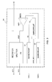
- FIG. 1 is a block diagram of an illustrative embodiment of a regulator circuit according to aspects of the present invention
- FIG. 2 is a block diagram of illustrative embodiment of another regulator circuit according to aspects of the present invention.
- FIG. 3 is a schematic diagram of an illustrative embodiment of the feed-forward circuit of FIG. 2 according to aspects of the present invention
- FIG. 4 is a schematic diagram of an illustrative embodiment of the rectifier/splitter of FIG. 3 according to aspects of the present invention
- FIG. 5 is a schematic diagram of an embodiment of the control circuitry of FIG. 2 according to aspects of the present invention.
- FIG. 6 is a schematic diagram of an illustrative embodiment of the output stage of FIG. 2 according to aspects of the present invention.
- FIGS. 7A-7F are timing diagrams illustrating waveforms of illustrative embodiments of signals for an embodiment of the regulation system of FIGS. 2-6 ;
- FIG. 8 is a block diagram of illustrative embodiment of yet another regulator circuit according to aspects of the present invention.
- FIG. 9 is a schematic diagram of an illustrative embodiment of the feed-forward circuit of FIG. 8 according to aspects of the present invention.
- FIG. 10 is a block diagram of an illustrative embodiment of the control circuitry of FIG. 8 according to aspects of the present invention.
- FIGS. 11A-11E are timing diagrams illustrating waveforms of embodiments of signals for an illustrative embodiment of the regulation system of FIGS. 8-10 ;
- FIGS. 12A-12E are timing diagrams illustrating waveforms of illustrative embodiments of signals for an embodiment of the regulation system of FIGS. 8-10 ;
- FIG. 13 is a block diagram of another illustrative embodiment of the control circuitry of FIG. 8 according to aspects of the present invention.
- Coupled means at least either a direct electrical connection between the items connected, or an indirect connection through one or more passive or active intermediary devices.
- circuit means at least either a single component or a multiplicity of components, either active and/or passive, that are coupled together to provide a desired function or functions.
- signal means at least one current, voltage, charge, temperature, data, or other signal.
- a “signal” may be used to communicate using active high, active low, time multiplexed, synchronous, asynchronous, differential, single-ended, or any other digital or analog signaling or modulation techniques.
- a “signal” may also be employed to provide and/or transmit power.
- FET field effect transistor
- bipolar transistor a bipolar transistor
- the scope of the words “gate”, “drain”, and “source” includes “base”, “collector”, and “emitter”, respectively, and vice versa.
- the phrase “in one embodiment,” as used herein does not necessarily refer to the same embodiment, although it may.
- the invention relates to a switching regulator with an error amplifier circuit and a feed-forward circuit.
- the error amplifier circuit provides an error signal by amplifying the difference between a feedback signal and a reference signal.
- the feed-forward circuit level-shifts the output of the error amplifier based on the feed-forward input signal and a scaling factor.
- the resulting adjusted error signal includes both feed-back and feed-forward signal components.
- a PWM (Pulse Width Modulation) comparator is employed to compare the adjusted error signal to a ramp signal. Switched-mode regulation is performed based on the PWM comparator output.
- buck-boost mode transition smoothing circuitry may also be employed to smooth the buck-mode/boost-mode transition in a buck-boost switching regulator.
- FIG. 1 is a block diagram of an illustrative embodiment of regulator 100 .
- Regulator 100 includes feed-forward circuit 110 , control circuitry 120 , output stage 130 , resistor R 1 , resistor R 2 , and error amplifier EA 1 .
- Regulator 100 is arranged to regulate output voltage VOUT to a substantially constant voltage over a range of input voltages of input voltage VDD.
- regulator 100 may be arranged to regulate output voltage VOUT to +12 volts, +3.3 volts, +1.8 volts, ⁇ 5 volts, and/or the like.
- regulator 100 is arranged provide feed-forward regulation of output voltage VOUT based, in part, on feed-forward input signal FF_IN.
- Control circuitry 120 is arranged to receive adjusted error signal VC′ and to provide switch control signals SCTL_ 1 -SCTL_ 4 based, at least in part, on adjusted error signal VC′.
- Output stage 130 is arranged to receive input voltage VDD and switch control signals SCTL_ 1 -SCTL_ 4 .
- Output stage 130 is further arranged to provide output voltage VOUT from input voltage VDD based, at least in part, on switch control signals SCTL_ 1 -SCTL_ 4 .
- output stage 130 is coupled to positive input voltage VDD and to ground.
- output stage 130 may be coupled between a positive input power supply and a negative input power supply, between ground and a negative power supply, between two positive power supplies, and/or the like.
- Feedback voltage divider resistors R 1 and R 2 are arranged to receive output voltage VOUT and to provide feedback signal VFB to error amplifier EA 1 .
- the values of resistors R 1 and R 2 may be selected to regulate the output voltage VOUT to any value.
- other feedback and/or sense circuits may be suitably employed to provide similar functionality.
- these circuits include current sense resistors, feedback amplifier circuits, transformers, hall-effect sensors, digital feedback control circuits, reference signal voltage divider, a reference signal amplifier circuit, a feedback signal amplifier circuit, and/or the like.
- feedback signal VFB is provided directly from output voltage VOUT.
- Error amplifier EA 1 is arranged to receive feedback signal VFB, to receive set-point signal VSET, and to provide error signal VC.
- error amplifier circuit EA 1 is arranged to provide error signal VC based, at least in part, on the difference between feedback signal VFB and set-point signal VSET.
- error amplifier EA 1 may include compensation circuitry, and/or the like.
- set-point signal VSET is employed as a set-point signal to define the value to which output voltage VOUT is regulated to.
- set-point signal VOUT is provided by a reference generator circuit such as a band-gap reference circuit.
- regulators, Zener diodes, gas-filled tubes, digital-to-analog converters, and/or the like may be suitably employed, instead of, or in conjunction with, a band-gap circuit.
- set-point signal VSET is a user controllable signal which may be changed, for example, to change the value of output voltage VOUT.
- set-point signal VSET may be provided by a digital-to-analog converter, a potentiometer, and/or the like.
- Feed-forward circuit 110 is arranged to receive error signal VC and to receive feed-forward input signal FF_IN. Feed-forward circuit 110 is further arranged to provide adjusted error signal VC′ based, at least in part, on error signal VC and feed-forward input signal FF_IN. In one illustrative embodiment, feed-forward circuit 110 is arranged to provide a pre-defined adjustment of error signal VC on adjusted error signal VC′ for a given value of feed-forward input signal FF_IN. For example, in one embodiment, feed-forward circuit 110 is arranged to provide adjusted error signal VC′ by level-shifting error signal VC by an amount that is based on feed-forward input signal FF_IN.
- feed-forward circuit 110 is arranged to provide feed-forward adjustment of adjusted error signal VC′ such that the lag time between a change on feed-forward input signal FF_IN and the corresponding change to output voltage VOUT is reduced.
- feed-forward circuit 110 may enable regulator 100 to respond to feed-forward input signal FF_IN changes without the delay commonly associated with feedback regulation systems.
- the regulator may be enabled to respond to feed-forward input signal FF_IN changes without the delays which are typically associated the inductor(s) and/or capacitor(s), of certain switching regulator topologies.
- regulator 100 differs from the described embodiments.
- feed-forward circuit 110 may be arranged to provide a feed-forward adjustment of a feedback signal instead of an error signal.
- feed-forward input signal FF_IN, set-point signal VSET, and/or the like may be provided via a voltage divider, buffer, gain circuit, and/or the like.
- control circuitry 120 may be arranged to receive an enable signal, mode control signal, and/or the like.
- regulator 100 may be a buck-mode, a boost-mode regulator, a fly-back regulator, a buck-boost regulator, a linear regulator, a half-bridge regulator, a full-bridge regulator, a switched capacitor regulator, an inverting regulator, and/or the like.
- regulator 100 may be either a current regulator and/or a voltage regulator, and may employ either current mode and/or voltage mode control.
- regulator 100 is a switching regulator, it may be a pulse-width modulated (PWM), pulse-frequency modulated (PFM), a PWM/PFM hybrid, and/or the like.
- PWM pulse-width modulated
- PFM pulse-frequency modulated
- PWM/PFM hybrid PWM/PFM hybrid
- switching regulator embodiments of regulator 100 may be synchronously or asynchronously rectified.
- FIG. 2 is a block diagram of an embodiment of regulator 200 .
- Regulator 200 includes feed-forward circuit 210 , control circuitry 220 , output stage 230 , resistor R 1 , resistor R 2 , and error amplifier EA 1 .
- Regulator 200 is arranged to regulate output voltage VOUT to a substantially constant voltage over a range of input voltages of input voltage VDD.
- Regulator 200 may be employed as an embodiment of regulator 100 of FIG. 1 .
- Control circuitry 220 , output stage 230 , resistor R 1 , resistor R 2 , and error amplifier EA 1 may be employed as respective embodiments of control circuitry 120 , output stage 130 , resistor R 1 , resistor R 2 , and error amplifier EA 1 of FIG. 1 .
- regulator 200 is a synchronously rectified buck-boost switching regulator.
- Feed-forward circuit 210 is arranged to receive error signal VC, to receive input voltage VDD as a feed-forward input signal and to receive set-point signal VSET as another feed-forward input signal. Feed-forward circuit 210 is further arranged to provide signals VC′ 1 and VC′ 2 based, at least in part, on error signal VC, input voltage VDD, and set-point signal VSET.
- input voltage VDD is an embodiment of feed-forward input signal FF_IN of FIG. 1 .
- set-point signal VSET is another illustrative embodiment of feed-forward input signal FF_IN of FIG. 1 .
- feed-forward circuit 210 is arranged to provide feed-forward adjustment of an internal reference voltage (not shown in FIG. 2 ) such that any disturbance due to a change on input voltage VDD is reduced.
- an internal reference voltage not shown in FIG. 2
- a change to input voltage VDD due to, for example, battery discharge, battery charging, output current changes, and/or the like
- the duration of this disturbance is related, in part, to the feedback loop lag time through control circuitry 220 , output stage 230 , and error amplifier EA 1 .
- the feed-forward adjustment based on input voltage VDD enables control circuitry 220 to provide a predetermined adjustment to the regulation of output voltage VOUT without the feedback delay through control circuitry 220 , output stage 230 , and error amplifier EA 1 .
- this feed-forward adjustment enables a reduced disturbance on output voltage VOUT.
- feed-forward circuit 210 is further arranged to provide feed-forward adjustment of the internal reference voltage (not shown in FIG. 2 ) such that the response time to a change on set-point signal VSET is reduced.
- the internal reference voltage not shown in FIG. 2
- feed-forward circuit 210 is further arranged to provide feed-forward adjustment of the internal reference voltage (not shown in FIG. 2 ) such that the response time to a change on set-point signal VSET is reduced.
- error signal VC is employed to control the regulation provided by regulator 200
- a change to set-point signal VSET (due to, for example, a request to change output voltage VOUT) the resulting change to output voltage VOUT may be delayed by the feedback loop lag time through control circuitry 220 , output stage 230 , and error amplifier EA 1 .
- the feed-forward adjustment based on set-point signal VSET enables control circuitry 220 to provide a predetermined adjustment to the regulation of output voltage VOUT without a feedback delay through control circuitry 220 , output stage 230 , and error amplifier EA 1 .
- this feed-forward adjustment enables a decreased response time and/or improved step response to a change on set-point signal VSET.
- Control circuitry 220 is arranged to receive signals VC′ 1 and VC′ 2 . Control circuitry 220 is further arranged to provide switch control signals SCTL_ 1 -SCTL_ 4 to output stage 230 based, at least in part, on signals VC′ 1 and VC′ 2 . In one embodiment, output stage 230 is arranged to regulate output voltage VOUT based, at least in part, on switch control signals SCTL_ 1 -SCTL_ 4 .
- feed-forward circuit 210 and control circuitry 220 further include mode-transition smoothing circuitry to smooth the transition between buck-mode operation and boost-mode operation in a buck-boost switching regulator.
- mode-transition smoothing circuitry may be omitted.
- FIG. 3 is a schematic diagram of an embodiment of feed-forward circuit 310 .
- Feed-forward circuit 310 includes gain circuits G 1 , G 2 , and G 3 , amplifier AMP 1 , and rectifier/splitter 312 .
- Feed-forward circuit 310 may be employed as an embodiment of feed-forward circuit 210 of FIG. 2 .
- Gain circuits G 1 and G 2 are arranged to provide scaled signal VG by multiplying input voltage VDD with constant K1, multiplying internal reference voltage VREF_INT with constant K2, and summing the results of the two multiplications.
- gain circuit G 3 is arranged to provide scaled set-point signal VSETG by multiplying set-point signal VSET with constant K3.
- Gain circuits G 1 , G 2 , and G 3 may be any suitable gain circuits.
- gain circuits G 1 , G 2 , and G 3 are non-inverting operational amplifier circuits.
- gain circuits G 1 , G 2 , and G 3 may be attenuation circuits, other operational amplifier circuits, and/or the like.
- one or more of gain circuits G 1 , G 2 , and G 3 may be omitted.
- Amplifier AMP 1 is arranged to provide adjusted reference signal VREF′ based, at least in part, on scaled signal VG and scaled set-point signal VSETG.
- Any suitable circuit may be employed as amplifier AMP 1 .
- operational amplifier circuits, summing amplifiers, level shifters, and/or the like may be suitably employed.
- constants K1, K2, and K3 are predetermined constants. Each of constants K1, K2, and K3 may be less than one, greater than one, or substantially equal to one. In one embodiment, constants K1, K2, and K3 are predetermined based on the expected effect of a given change to input voltage VDD or set-point signal VSET on regulated output voltage VOUT. For example, constants K1, K2, and K3 may be calculated by simultaneously solving multiple equations which define values of output voltage VOUT for various values of input voltage VDD and set-point signal VSET. In one illustrative embodiment, the multiple equations are solved to determine a switching regulator PWM duty cycle to produce a given value of output voltage VOUT.
- constants K1, K2, and K3 are calculated to minimizing the output disturbance on regulated output voltage VOUT resulting from a fixed step on input voltage VDD over a wide operating range for output voltage VDD.
- a voltage step may be fixed at approximately 0.6 volts.
- constants K1, K2, and K3 may be calculated to minimize disturbances for voltage step changes of any magnitude.
- constants K1, K2, and K3 are calculated to reduce the variance on error signal VC and to improve the output dynamic range of an error amplifier (such as error amplifier EA 1 of FIG. 2 ) over a wide operating range for output voltage VDD.
- Rectifier/splitter 312 is arranged to provide signals VC′ 1 and VC′ 2 based, in part, on error signal VC and adjusted error signal VC′. Further, in one embodiment, rectifier/splitter 312 is operable to provide signals VC′ 1 and VC′ 2 such that they are proportional to the departure of error signal VC from a central value defined by adjusted reference signal VREF′ but increasing in value from zero. Only one of the two signals VC′ 1 and VC′ 2 departs from zero depending on adjusted error signal VC′ and adjusted reference signal VREF′.
- FIG. 4 illustrates a schematic diagram of an embodiment of rectifier/splitter 412 .
- Rectifier/splitter 412 includes resistors RRS 1 -RRS 8 , operational amplifier ARS 1 , and operational amplifier ARS 2 .
- Rectifier/splitter 412 may be employed as embodiment of rectifier/splitter 312 of FIG. 3 .
- Operational amplifier ARS 1 and resistors RRS 1 -RRS 4 are arranged to operate as a differential amplifier.
- Operational amplifier ARS 2 and resistors RRS 5 -RRS 8 are arranged to operate as another differential amplifier.
- error signal VC is applied to the inverting input of the differential amplifier that includes operational amplifier ARS 1 , so that signal VC′ 1 is inverted relative to error signal VC.
- signal VC′ 2 is level-shifted, amplified, and clamped such that voltage VC′ 2 cannot be lower than zero volts.
- signal VC′ 1 is inverted, level-shifted, amplified, and clamped such that signal VC′ 1 cannot be lower than zero volts.
- signal VC′ 1 reaches zero volts when the buck regulation reaches 100% duty cycle.
- signal VC′ 2 reaches zero volts when the boost regulation reaches 0% duty cycle.
- the voltage of signals VC′ 1 and VC′ 2 are both zero volts. Operation of rectifier/splitter 412 during the pass-through transition is discussed in further detail below, for one embodiment.
- Adjusted reference voltage VREF′ may be provided by amplifier AMP 1 of FIG. 3 , and/or the like.
- rectifier/splitter 412 Although a particular embodiment of rectifier/splitter 412 is illustrated in FIG. 4 , other embodiments of the rectifier/splitter are within the scope and spirit of the invention.
- FIG. 5 is a schematic diagram of an embodiment of control circuitry 520 .
- Control circuitry 520 includes ramp circuit R 1 , comparator COMP 1 , comparator COMP 2 , and drive circuit DRV 1 .
- Control circuitry 520 may be employed as an embodiment of control circuitry 220 of FIG. 2 .
- FIG. 6 is a schematic diagram of an embodiment of output stage 630 .
- Output stage 630 includes transistors M 1 -M 4 , inductor L 1 , and capacitor COUT. Output stage 630 may be employed as an embodiment of output stage 230 of FIG. 2 .
- control circuitry 520 and output stage 630 are discussed together, below, for one embodiment.
- Control circuitry 520 is arranged to receive signals VC′ 1 and VC′ 2 and to provide switch control signals SCTL 1 -SCTL 4 based, at least in part, on signals VC′ 1 and VC′ 2 .
- Output stage 630 is arranged to regulated output voltage VOUT from input voltage VDD based, at least in part, on switch control signals SCTL 1 -SCTL 4 .
- control circuitry 520 is arranged as a portion of a PWM modulated buck/boost regulator controller and output stage 630 is arranged as a portion of a PWM modulated buck/boost regulator. In one such embodiment, at any given time during operation, control circuitry 520 and output stage 630 operates in either buck mode or boost mode.
- switches M 1 and M 3 are closed, and switches M 2 and M 4 are open, so that node IN is coupled to node OUT via inductor L 1 .
- control circuitry 520 controls the switches such that: switch M 3 is always closed and switch M 4 is always open. Also, control circuitry 520 controls switches M 1 and M 2 during buck regulation according to PWM buck switching regulation to provide regulated power signal VOUT.
- control circuitry 520 controls the switches such that: switch M 1 is always closed and switch M 2 is always open. Also, control circuitry 520 controls switches M 3 and M 4 during boost regulation according to PWM boost switching regulation to provide regulated power signal VOUT.
- ramp circuit R 1 is a modulation waveform generation circuit that generates ramp signal VRAMP.
- ramp signal VRAMP may be a sawtooth waveform that linearly ramps from a value slightly greater than zero (e.g. 0.1 mV) to a maximum value related to the range of the control voltage and the desired minimum duty cycle.
- comparator COMP 1 is operable to compare signal VC′ 1 with ramp signal VRAMP, and to provide buck PWM signal BUCK based on the comparison.
- comparator COMP 2 is operable to compare signal VC′ 2 with ramp signal VRAMP, and to provide boost PWM signal BOOST based on the comparison.
- drive circuit DRV 1 is operable to drive switches M 1 , M 2 , M 3 , and M 4 based on signals BOOST and BUCK.
- Control circuitry 520 operates in two modes, buck and boost, and in one embodiment, the ripple is less than 30 mV during the mode transition.
- control circuitry 520 and output stage 630 is illustrated in FIGS. 5 and 6 , many variations of this circuit are within the scope and spirit of the invention.
- the logic shown may be reversed or otherwise modified from the exact logic shown.
- each of switches M 1 -M 4 may be selected to correspond to either an active high or an active low control signal.
- FIG. 6 illustrates an embodiment in which input voltage VDD is provided by a battery. However, in other embodiments, input voltage VDD may be provided from a source other than a battery. As yet another example, FIG. 6 illustrates a synchronously-rectified embodiment of output stage 630 .
- output stage 630 is an asynchronous-rectified regulator, and switches M 2 and M 4 are replaced with diodes. Further, illustrative embodiments of control circuitry 520 and output stage 630 may include more or less components than illustrated in FIGS. 5 and 6 .
- the modulating waveform may be any waveform suitable as a pulse width modulating waveform, such as a triangle wave, or the like.
- the switches M 1 , M 2 , M 3 , and M 4 are shown in FIG. 6 , other embodiments of the switches are within the scope and spirit of the invention.
- field effect transistors are illustrated in FIG. 6
- bipolar transistors or the like may instead by used.
- p-type transistors and/or n-type transistors, and vice versa may be employed with suitable control logic. These embodiments and others are within the scope and spirit of the invention.
- FIGS. 7A-7F shows a timing diagram of waveforms of embodiments of signals for an embodiment of the circuitry of FIGS. 2-6 .
- FIGS. 7A-7F illustrate waveforms of particular embodiments of signals for one embodiment of the circuitry of FIGS. 2-6 , the invention is not so limited.
- FIGS. 7A-7F are shown by way of example and illustration only. Other illustrative embodiments of circuitry having waveforms different than shown in FIGS. 7A-7F may be employed within the scope and spirit of the invention.
- FIG. 7A illustrates a timing diagram of a waveform an embodiment of error signal VC.
- FIG. 7B shows a timing diagram of a waveform an embodiment of signal VC′ 1 .
- FIG. 7C illustrates a timing diagram of a waveform an embodiment of signal VC′ 2 .
- FIG. 7D shows a timing diagram of a waveform an embodiment of ramp signal VRAMP.
- FIG. 7E illustrates a timing diagram of a waveform an embodiment of signal BUCK.
- FIG. 7F shows a timing diagram of a waveform an embodiment of signal BOOST.
- Region I represents buck mode operation
- region III represents boost mode operation
- region II represents the mode transition between buck mode and boost mode operation.
- buck mode occurs when error signal VC is less than V 1
- boost mode occurs when error signal VC is greater than V 2
- the mode transition occurs when error signal VC is greater than V 1 but less than V 2 .
- FIG. 7A shows error signal VC ramping upward. This may occur, for example, as a result of the input voltage VDD dropping.
- the PWM control signal BUCK of the input pair power switches is generated from signal VC′ 1 and from ramp signal VRAMP.
- control circuitry 420 is operating in buck mode and the duty cycle is zero.
- error signal VC ramps upward from zero signal VC′ 1 ramps downward from VREF 1 .
- VC′ 1 ramps downward, the duty cycle of buck PWM signal BUCK increases.
- the duty cycle of signal BUCK is inversely proportional to VC′ 1 .
- the duty cycle of signal BUCK reaches 100% when VC′ 1 reaches 0V.
- control of the transition region between modes is made relatively precise by adjusting the value of V 1 and offsetting the inputs of the comparator.
- the mode transition occurs when VC′ 1 and VC′ 2 are both below VRAMP, as opposed to an embodiment in which the logic is reversed in such a way that the mode transition occurs when VC′ 1 and VC′ 2 are both above VRAMP.
- V 2 -V 1 is independent of the VRAMP peak value. Normally the peak of the ramp can vary considerably over the variation of supply voltage and ambient temperature.
- V 2 -V 1 depends on the peak value of VRAMP and has larger variation.
- region II is described as a mode transition, it is not necessarily the case that the regulator must transition to the opposite mode when region II is entered. For example, if the regulator is operating in region I, and later passes into region II, it is not necessarily the case that the regulator will transition into region III. It is also possible that the regulator may return to region I, and may then either remain in region I or oscillate back and forth between region I and II for a time.
- Signal VC′2 is clamped at zero as long as error signal VC is less than V 2 . Further, signal VC′ 2 follows error signal VC if error signal VC is greater than V 2 .
- FIG. 8 is a block diagram of an embodiment of regulator 800 .
- Regulator 800 includes feed-forward circuit 810 , control circuitry 820 , output stage 830 , resistor R 1 , resistor R 2 , and error amplifier EA 1 .
- Regulator 800 is arranged to regulate output voltage VOUT to a substantially constant voltage over a range of input voltages of input voltage VDD.
- Regulator 800 may be employed as an embodiment of regulator 100 of FIG. 1 .
- Control circuitry 820 , output stage 830 , resistor R 1 , resistor R 2 , and error amplifier EA 1 may be employed as respective embodiments of control circuitry 120 , output stage 130 , resistor R 1 , resistor R 2 , and error amplifier EA 1 of FIG. 1 .
- regulator 800 is a synchronously rectified buck-boost switching regulator.
- Feed-forward circuit 810 is arranged to receive error signal VC, to receive input voltage VDD as a feed-forward input signal and to receive set-point signal VSET as another feed-forward input signal. Feed-forward circuit 810 is further arranged to provide adjusted error signal VC′ based, at least in part, on error signal VC, input voltage VDD, and set-point signal VSET.
- input voltage VDD is an embodiment of feed-forward input signal FF_IN of FIG. 1 .
- set-point signal VSET is another embodiment of feed-forward input signal FF_IN of FIG. 1 .
- feed-forward circuit 810 is arranged to provide feed-forward adjustment of adjusted error signal VC′ such that any disturbance due to a change on input voltage VDD is reduced.
- error signal VC is employed to control the regulation provided by regulator 800
- a change to input voltage VDD may result in a disturbance on output voltage VOUT.
- the duration of this disturbance is related, in part, to the feedback loop lag time through control circuitry 820 , output stage 830 , and error amplifier EA 1 .
- the feed-forward adjustment based on input voltage VDD enables control circuitry 820 to provide a predetermined adjustment to the regulation of output voltage VOUT without a feedback delay through control circuitry 820 , output stage 830 , and error amplifier EA 1 .
- this feed-forward adjustment enables a reduced disturbance on output voltage VOUT.
- feed-forward circuit 810 is further arranged to provide feed-forward adjustment of adjusted error signal VC′ such that the response time to a change on set-point signal VSET is reduced.
- error signal VC is employed to control the regulation provided by regulator 800
- a change to set-point signal VSET (due to, for example, a request to change output voltage VOUT) the resulting change to output voltage VOUT may be delayed by the feedback loop lag time through control circuitry 820 , output stage 830 , and error amplifier EA 1 .
- the feed-forward adjustment based on set-point signal VSET enables control circuitry 800 to provide a predetermined adjustment to the regulation of output voltage VOUT without a feedback delay through control circuitry 820 , output stage 830 , and error amplifier EA 1 .
- this feed-forward adjustment enables a decreased response time and/or improved step response to a change on set-point signal VSET.
- Control circuitry 820 is arranged to receive adjusted error signal VC′. Control circuitry 820 is further arranged to provide switch control signals SCTL_ 1 -SCTL_ 4 to output stage 830 based, at least in part, on adjusted error signal VC′. In one embodiment, output stage 830 is arranged to regulate output voltage VOUT based, at least in part, on switch control signals SCTL_ 1 -SCTL_ 4 .
- feed-forward circuit 810 and control circuitry 820 further include mode-transition smoothing circuitry to smooth the transition between buck-mode operation and boost-mode operation in a buck-boost switching regulator.
- mode-transition smoothing circuitry may be omitted.
- FIG. 9 is a schematic diagram of an embodiment of feed-forward circuit 910 .
- Feed-forward circuit 910 includes amplifier AMP 2 and gain circuits G 1 , G 3 , and G 4 .
- Feed-forward circuit 910 may be employed as an embodiment of feed-forward circuit 810 of FIG. 8 .
- Gain circuits G 1 and G 3 may be employed as respective embodiments of gain circuits G 1 and G 3 of FIG. 3 .
- gain circuit G 4 is arranged to provide scaled error signal VCG by multiplying error signal VC with constant K4.
- Gain circuit G 4 may be any suitable gain circuits, such as those discussed above. In certain embodiments, one or more of gain circuits G 1 , G 3 , and G 4 may be omitted.
- Amplifier AMP 2 is arranged to provide adjusted error signal VC′ based, at least in part, on scaled error signal VCG, scaled power signal VDDG, and scaled set-point signal VSETG.
- Any suitable circuit may be employed as amplifier AMP 2 .
- operational amplifier circuits, summing amplifiers, level shifters, and/or the like may be suitably employed.
- constants K1, K3, and K4 are predetermined constants. Each of constants K1, K3, and K4 may be less than one, greater than one, or substantially equal to one. In one embodiment, constants K1, K3, and K4 are predetermined based on the expected effect of a given change to input voltage VDD, set-point signal VSET, or error signal VC, on output voltage VOUT. For example, constants K1, K3, and K4 may be calculated by simultaneously solving multiple equations which define values of output voltage VOUT for various values of input voltage VDD and set-point signal VSET. In one embodiment, the multiple equations are solved to determine a switching regulator PWM duty cycle to produce a given value of output voltage VOUT.
- constants K1, K3, and K4 are calculated to minimizing the output disturbance on regulated output voltage VOUT resulting from a fixed step on input voltage VDD over a wide operating range for output voltage VDD.
- a voltage step may be fixed at approximately 0.6 volts.
- constants K1, K3, and K4 may be calculated to minimize disturbances for voltage step changes of any magnitude.
- constants K1, K3, and K4 are calculated to reduce the variance on error signal VC and to improve the output dynamic range of an error amplifier (such as error amplifier EA 1 of FIG. 8 ) over a wide operating range for output voltage VDD.
- FIG. 10 is a block diagram of an embodiment of control circuitry 1020 .
- Control circuitry 1020 includes ramp circuit R 2 , comparator COMP 1 , comparator COMP 2 , nor gate NOR 1 , nand gate NAND 1 , and drive circuit DRV 1 .
- Control circuitry 1020 may be employed as an embodiment of control circuitry 820 of FIG. 8 .
- Control circuitry 1020 is arranged to receive adjusted error signal VC′ and to provide switch control signals SCTL 1 -SCTL 4 based, at least in part, on adjusted error signal VC′.
- output stage 630 of FIG. 6 may be employed in conjunction with control circuitry 1020 to regulated output voltage VOUT from input voltage VDD.
- other output stages may be suitably employed.
- control circuitry 1020 is arranged as a portion of a PWM modulated buck/boost regulator controller. In one such embodiment, at any given time during operation, control circuitry 1020 controls either buck-mode or boost-mode operation. Further, during the transition period between the buck-mode operation and boost mode operation, control circuitry provides switch control signals SCTL_ 1 -SCTL_ 4 such that switches M 1 and M 3 are closed, and switches M 2 and M 4 are open, and node IN is effectively coupled to node OUT via inductor L 1 .
- ramp circuit R 1 is a modulation waveform generation circuit that generates ramp signals VRAMP 1 and VRAMP 2 .
- each of ramp signals VRAMP 1 and VRAMP 2 may be saw-tooth waveforms that linearly ramps from a value slightly greater than zero (e.g. 0.1 mV) to a maximum value related to the range of the control voltage and the desired minimum duty cycle.
- ramp signals VRAMP 1 and VRAMP 2 are provided with a fixed amplitude and are approximately 180 degrees out of phase with respect to each other.
- the modulation waveform generator may generate other waveforms suitable as a pulse width modulating waveform, such as a triangle wave, or the like.
- other methods of PWM generation may be incorporated such as delta modulation, sigma-delta modulation, and digital modulation using counters.
- Comparator COMP 3 is arranged to assert (drive high) signal C 3 _OUT while ramp signal VRAMP 1 is greater than adjusted error signal VC′ and to de-assert (drive low) signal C 3 _OUT while ramp signal VRAMP 1 is less than adjusted error signal VC′.
- comparator COMP 4 is arranged to assert (drive high) signal C 4 _OUT while ramp signal VRAMP 2 is greater than adjusted error signal VC′ and to de-assert (drive low) signal C 4 _OUT while ramp signal VRAMP 2 is less than adjusted error signal VC′.
- Comparators COMP 3 and COMP 4 may be any suitable comparison circuits. For example, high gain differential amplifiers, hysteretic comparators, differential amplifiers, and/or the like, may be suitably employed. In one embodiment, comparators COMP 3 and/or comparator COMP 4 includes trimming circuitry to provide timing compensation due to non-ideal phase shifting of ramp signals VRAMP 1 and VRAMP 2 .
- Nor gate NOR 1 and nand gate NAND 1 are arranged to provide regulation control signals BOOST and BUCK based, at least in part, on the output of comparators COMP 3 and COMP 4 .
- regulation control signal BOOST is asserted (for example, to close boost low side switch M 4 ) while signals C 3 _OUT and C 4 _OUT are both low to indicate that adjusted error signal VC′ is greater than ramp signal VRAMP 1 and is greater than ramp signal VRAMP 2 .
- regulation control signal BUCK is asserted (for example, to open buck high side switch M 1 ) while signals C 3 _OUT and C 4 _OUT are both high to indicate that adjusted error signal VC′ is less than ramp signal VRAMP 1 and is less than ramp signal VRAMP 2 .
- signals C 3 _OUT and C 4 _OUT are both high to indicate that adjusted error signal VC′ is less than ramp signal VRAMP 1 and is less than ramp signal VRAMP 2 .
- other logic levels and logic circuitry may be suitably employed.
- drive circuit DRV 1 is operable to drive switches M 1 , M 2 , M 3 , and M 4 based on signals BOOST and BUCK.
- control circuitry 1020 enables smooth transitions between buck-mode operation and boost-mode operation, and vice-versa, in a buck-boost regulator.
- Control circuitry 1020 may also be employed in a buck-boost regulator without a feed-forward circuit.
- control circuitry 1020 may be arranged to receive error signal VC from an error amplifier, and/or the like.
- FIGS. 11A-11E shows a timing diagram of waveforms of embodiments of signals for an embodiment of the circuitry of FIGS. 8-10 .
- FIGS. 11A-11E illustrate waveforms of particular embodiments of signals for one embodiment of the circuitry of FIGS. 8-10 , the invention is not so limited.
- FIGS. 11A-11E are shown by way of example and illustration only. Other embodiments of circuitry having waveforms different than shown in FIGS. 11A-11E may be employed within the scope and spirit of the invention.
- FIG. 11A illustrates a timing diagram of a waveform an embodiment of ramp signal VRAMP 1 .
- FIG. 11C shows a timing diagram of a waveform an embodiment of ramp signal VRAMP 2 .
- FIG. 11B illustrates a timing diagram of a waveform an embodiment of adjusted error signal VC′.
- FIG. 11D shows a timing diagram of a waveform an embodiment of regulation signal BUCK.
- FIG. 11E shows a timing diagram of a waveform an embodiment of regulation signal BOOST.
- region I represents buck mode operation
- region III represents boost mode operation
- region II represents the mode transition between buck mode and boost mode operation.
- buck mode occurs when adjusted error signal VC′ is less than the intersection voltage value of ramp signals VRAMP 1 and VRAMP 2 (for example, the mid-point voltage of either of ramp signals VRAMP 1 or VRAMP 2 ).
- boost mode occurs when adjusted error signal VC′ is greater than the intersection of ramp signals VRAMP 1 and VRAMP 2
- the mode transition occurs when adjusted error signal VC is equal to the intersection of ramp signals VRAMP 1 and VRAMP 2 .
- the duty cycle of regulation signal BUCK is relatively low as the percentage of time during which VC is less than both ramp signal VRAMP 1 and ramp signal VRAMP 2 is relatively long.
- the duty cycle of regulation signal BUCK rises until it is reaches 100%.
- the rise of regulation signal BUCK duty cycle to 100% corresponds to the increase of adjusted error signal VC′ such that the percentage of time during which adjusted error signal VC′ is less than both ramp signal VRAMP 1 and ramp signal VRAMP 2 decreases.
- the regulator reaches the buck-boost transition at region II.
- regulation signal BUCK has a duty cycle of approximately 100% and regulation signal BOOST has a duty cycle of approximately 0%.
- the duty cycle of regulation signal BUCK remains at 100% as the duty cycle of regulation signal BOOST rises from 0%.
- the duty cycle of regulation signal BOOST is substantially equal to the percentage of time that adjusted error signal VC′ is greater than both ramp signal VRAMP 1 and ramp signal VRAMP 2 .
- region II is described as a mode transition, it is not necessarily the case that the regulator must transition to the opposite mode when region II is entered. For example, if the regulator is operating in region I, and later passes into region II, it is not necessarily the case that the regulator will transition into region III. It is also possible that the regulator may return to region I, and may then either remain in region I or oscillate back and forth between region I and II for a time. Further, for one embodiment, ramp signals VRAMP 1 and VRAMP 2 may be saw-tooth signals instead of triangular signals.
- FIGS. 12A-12E shows a timing diagram of waveforms of embodiments of signals for an embodiment of the circuitry of FIGS. 8-10 .
- FIGS. 12A-12E illustrate waveforms of particular embodiments of signals for one embodiment of the circuitry of FIGS. 8-10 , the invention is not so limited.
- FIGS. 12A-12E are shown by way of example and illustration only. Other embodiments of circuitry having waveforms different than shown in FIGS. 12A-12E may be employed within the scope and spirit of the invention.
- FIG. 12A illustrates a timing diagram of a waveform an embodiment of ramp signal VRAMP 1 .
- FIG. 12C shows a timing diagram of a waveform an embodiment of ramp signal VRAMP 2 .
- FIG. 12B illustrates a timing diagram of a waveform an embodiment of adjusted error signal VC′.
- FIG. 12D shows a timing diagram of a waveform an embodiment of regulation signal BUCK.
- FIG. 12E shows a timing diagram of a waveform an embodiment of regulation signal BOOST.
- FIGS. 12A-12E illustrate the operation of one embodiment of control circuitry 1020 during the mode transition between buck mode and boost mode operation of region II.
- control circuitry 1020 is arranged to interleave buck-mode switching with boost mode-switching during the transition to further smooth the regulation of output voltage VOUT.
- buck-mode switching is interleaved with boost mode switching during region II operation by providing a slight phase deviation from the 180 degree phase shift between ramp signal VRAMP 1 and ramp signal VRAMP 2 .
- Such a phase deviation may cause the voltage level of the ramp signal VRAMP 1 and ramp signal VRAMP 2 intersection to change.
- ramp signal VRAMP 1 and ramp signal VRAMP 2 intersect at a first voltage at every other intersection.
- ramp signal VRAMP 1 and ramp signal VRAMP 2 intersect at a second voltage for each of the other intersections.
- the first voltage is slightly different than the second voltage.
- adjusted error signal VC is less than both ramp signal VRAMP 1 and ramp signal VRAMP 2 for a portion of one switching cycle and is greater than both ramp signal VRAMP 1 and ramp signal VRAMP 2 for a portion of the next switching cycle.
- FIG. 13 is a block diagram of an embodiment of control circuitry 1320 .
- Control circuitry 1320 includes ramp circuit R 2 , comparator COMP 1 , comparator COMP 2 , nor gate NOR 1 , nand gate NAND 1 , delay circuit DELAY 1 , delay circuit DELAY 2 , and drive circuit DRV 1 .
- Control circuitry 1320 may be employed as an embodiment of control circuitry 820 of FIG. 8 .
- delay circuits DELAY 1 and DELAY 2 are operable as leading edge delay circuits.
- rising edges of delayed signals D 1 _OUT and D 2 _OUT follow the respective rising edges of signals C 3 _OUT and C 4 _OUT by a delay period.
- the falling edges on delayed signals D 1 _OUT and D 2 _OUT follow the respective falling edges of signals C 3 _OUT and C 4 _OUT with substantially no delay.
- the rising edge delay provided by delay circuits DELAY 1 and DELAY 2 may be any suitable length and may be either fixed or adjustable and may be predetermined or calculated based on in-circuit operational parameters.
- the length the delay period is configured such that there is buck-boost regulation overlap during the transition period. This buck-boost regulation overlap may enable buck-mode switching to be interleaved with boost-mode switching during the transition period in one embodiment.
- dynamic comparator offsets may also be employed to provide, during mode-transition, interleaved pulses on regulation signal BUCK and on regulation signal BOOST.
- static comparator offsets may also be employed to provide, during mode-transition, interleaved pulses on regulation signal BUCK and on regulation signal BOOST.
- the same feed-forward and transition circuits and techniques may be incorporated in multi-phase buck-boost converter or regulator topologies.
- the output circuit 630 may be extended to include additional banks of switches M 1 ′-M 4 ′ (not shown) connected between the inputs to the block of circuit 630 and the OUT terminal in parallel with switches M 1 -M 4 and sharing the same output capacitor COUT.
Abstract
Description
VREF′=(VG)−(VSETG),
where in VG=(VDD*K1+VREF_INT*K2) and VSETG=(VSET*K3). Accordingly, in this embodiment, feed-
VREF′=(VDD*K1)+(VREF — INT*K2)−(VSET*K3).
Any suitable circuit may be employed as amplifier AMP1. For example, operational amplifier circuits, summing amplifiers, level shifters, and/or the like, may be suitably employed.
VC′=(VCG)+(VDDG)−(VSETG),
where in VDDG=(VDD*K1), VSETG=(VSET*K3), and VCG=(VC*K4). Accordingly, in this embodiment, feed-forward circuit 320 is arranged such that:
VC′=(VC*K4)+(VDD*K1)−(VSET*K3).
Any suitable circuit may be employed as amplifier AMP2. For example, operational amplifier circuits, summing amplifiers, level shifters, and/or the like, may be suitably employed.
Claims (33)
VC′=(FF — IN*K1)+(VC*K2),
VC′=(VC*K4)+(VDD*K1)−(VSET*K3),
VC′=(VC*K4)+(VDD*K1)−(VSET*K3),
Priority Applications (1)
| Application Number | Priority Date | Filing Date | Title |
|---|---|---|---|
| US12/136,010 US8106639B1 (en) | 2008-06-09 | 2008-06-09 | Feed forward control of switching regulator |
Applications Claiming Priority (1)
| Application Number | Priority Date | Filing Date | Title |
|---|---|---|---|
| US12/136,010 US8106639B1 (en) | 2008-06-09 | 2008-06-09 | Feed forward control of switching regulator |
Publications (1)
| Publication Number | Publication Date |
|---|---|
| US8106639B1 true US8106639B1 (en) | 2012-01-31 |
Family
ID=45508146
Family Applications (1)
| Application Number | Title | Priority Date | Filing Date |
|---|---|---|---|
| US12/136,010 Active 2030-10-09 US8106639B1 (en) | 2008-06-09 | 2008-06-09 | Feed forward control of switching regulator |
Country Status (1)
| Country | Link |
|---|---|
| US (1) | US8106639B1 (en) |
Cited By (6)
| Publication number | Priority date | Publication date | Assignee | Title |
|---|---|---|---|---|
| WO2013182249A1 (en) * | 2012-06-08 | 2013-12-12 | Telefonaktiebolaget L M Ericsson (Publ) | Controlling a switched mode power supply with maximised power efficiency |
| US20140035544A1 (en) * | 2011-04-13 | 2014-02-06 | Huawei Technologies Co., Ltd. | Hysteretic Control Conversion Circuit and Power Supply System |
| US8841971B1 (en) | 2012-12-17 | 2014-09-23 | Google Inc. | Short circuit current protection in an amplifier |
| US20170222463A1 (en) * | 2016-02-01 | 2017-08-03 | Qualcomm Incorporated | Duty cycle control for charging a battery |
| US10566902B1 (en) * | 2018-08-22 | 2020-02-18 | Semiconductor Components Industries, Llc | Methods and systems of operating buck-boost converters |
| US20220077767A1 (en) * | 2020-09-08 | 2022-03-10 | Delta Electronics (Shanghai) Co.,Ltd. | Startup control method and system, and voltage spike measurement circuit and method |
Citations (17)
| Publication number | Priority date | Publication date | Assignee | Title |
|---|---|---|---|---|
| US4809150A (en) | 1988-01-27 | 1989-02-28 | Electric Power Research Institute, Inc. | DC to DC converter with feed forward and feed back regulation |
| US5949224A (en) | 1997-08-06 | 1999-09-07 | Telefonaktiebolaget Lm Ericsson | Buck boost switching regulator |
| US6166926A (en) * | 2000-01-11 | 2000-12-26 | Thomson Licensing S.A. | Zero voltage switching power supply with burst mode |
| US6166527A (en) | 2000-03-27 | 2000-12-26 | Linear Technology Corporation | Control circuit and method for maintaining high efficiency in a buck-boost switching regulator |
| US6348781B1 (en) | 2000-12-11 | 2002-02-19 | Motorola, Inc. | Buck or boost power converter |
| US6515457B1 (en) | 2002-05-21 | 2003-02-04 | National Semiconductor Corporation | Discontinuous-mode buck-boost slave converter working off a continuous-mode master buck converter |
| US6538419B1 (en) * | 2000-01-11 | 2003-03-25 | Thomson Licensing S.A. | Power supply with synchronized power on transition |
| US6593725B1 (en) * | 2001-02-22 | 2003-07-15 | Cypress Semiconductor Corp. | Feed-forward control for DC-DC converters |
| US6897723B2 (en) * | 2000-12-22 | 2005-05-24 | Paradigm Wireless Communications, Llc | Feed-forward amplifier loop control utilizing if signal processing |
| US6900624B2 (en) | 2001-04-05 | 2005-05-31 | Toyota Jidosha Kabushiki Kaisha | DC-DC converter with feed-forward and feedback control |
| US6952355B2 (en) * | 2002-07-22 | 2005-10-04 | Ops Power Llc | Two-stage converter using low permeability magnetics |
| US6975525B2 (en) * | 2002-11-14 | 2005-12-13 | Fyre Storm, Inc. | Method of controlling the operation of a power converter having first and second series connected transistors |
| US7026800B2 (en) | 2002-10-17 | 2006-04-11 | Richtek Technology Corp. | Feed-forward method for improving a transient response for a DC—DC power conversion and DC—DC voltage converter utilizing the same |
| US7129680B2 (en) | 2002-11-20 | 2006-10-31 | Matsushita Electric Industrial Co., Ltd. | Voltage step-up and step-down DC/DC converter |
| US20090015217A1 (en) * | 2007-07-12 | 2009-01-15 | Harriman Paul J | Power supply controller and method therefor |
| US7598715B1 (en) * | 2007-04-04 | 2009-10-06 | National Semiconductor Corporation | Apparatus and method for reverse current correction for a switching regulator |
| US7868603B2 (en) * | 2006-10-04 | 2011-01-11 | Microsemi Corporation | Method and apparatus to compensate for supply voltage variations in a PWM-based voltage regulator |
-
2008
- 2008-06-09 US US12/136,010 patent/US8106639B1/en active Active
Patent Citations (17)
| Publication number | Priority date | Publication date | Assignee | Title |
|---|---|---|---|---|
| US4809150A (en) | 1988-01-27 | 1989-02-28 | Electric Power Research Institute, Inc. | DC to DC converter with feed forward and feed back regulation |
| US5949224A (en) | 1997-08-06 | 1999-09-07 | Telefonaktiebolaget Lm Ericsson | Buck boost switching regulator |
| US6538419B1 (en) * | 2000-01-11 | 2003-03-25 | Thomson Licensing S.A. | Power supply with synchronized power on transition |
| US6166926A (en) * | 2000-01-11 | 2000-12-26 | Thomson Licensing S.A. | Zero voltage switching power supply with burst mode |
| US6166527A (en) | 2000-03-27 | 2000-12-26 | Linear Technology Corporation | Control circuit and method for maintaining high efficiency in a buck-boost switching regulator |
| US6348781B1 (en) | 2000-12-11 | 2002-02-19 | Motorola, Inc. | Buck or boost power converter |
| US6897723B2 (en) * | 2000-12-22 | 2005-05-24 | Paradigm Wireless Communications, Llc | Feed-forward amplifier loop control utilizing if signal processing |
| US6593725B1 (en) * | 2001-02-22 | 2003-07-15 | Cypress Semiconductor Corp. | Feed-forward control for DC-DC converters |
| US6900624B2 (en) | 2001-04-05 | 2005-05-31 | Toyota Jidosha Kabushiki Kaisha | DC-DC converter with feed-forward and feedback control |
| US6515457B1 (en) | 2002-05-21 | 2003-02-04 | National Semiconductor Corporation | Discontinuous-mode buck-boost slave converter working off a continuous-mode master buck converter |
| US6952355B2 (en) * | 2002-07-22 | 2005-10-04 | Ops Power Llc | Two-stage converter using low permeability magnetics |
| US7026800B2 (en) | 2002-10-17 | 2006-04-11 | Richtek Technology Corp. | Feed-forward method for improving a transient response for a DC—DC power conversion and DC—DC voltage converter utilizing the same |
| US6975525B2 (en) * | 2002-11-14 | 2005-12-13 | Fyre Storm, Inc. | Method of controlling the operation of a power converter having first and second series connected transistors |
| US7129680B2 (en) | 2002-11-20 | 2006-10-31 | Matsushita Electric Industrial Co., Ltd. | Voltage step-up and step-down DC/DC converter |
| US7868603B2 (en) * | 2006-10-04 | 2011-01-11 | Microsemi Corporation | Method and apparatus to compensate for supply voltage variations in a PWM-based voltage regulator |
| US7598715B1 (en) * | 2007-04-04 | 2009-10-06 | National Semiconductor Corporation | Apparatus and method for reverse current correction for a switching regulator |
| US20090015217A1 (en) * | 2007-07-12 | 2009-01-15 | Harriman Paul J | Power supply controller and method therefor |
Non-Patent Citations (17)
| Title |
|---|
| Chakraborty et al., "Combination of Buck and Boost Modes to Minimize Transients in the Output of a Positive Buck-Boost Converter," IEEE 2006. pp. 2372-2377. |
| Chen et al., "Buck-Boost PWM Converters Having Two Independently Controlled Switches," 2001 IEEEE 32nd Annual Power Electronics Specialists Conference (PESC), 2(17-21):736-741 (2001). |
| Cheng et al., "Chaos Study and Parameter-Space Analysis of the DC-DC Buck-Boost Converter," IEE Proc.-Electr. Power Appl., 150(2):126-138 (2003). |
| Feng et al., "An Adaptive Current Mode Fuzzy Logic Controller for DC-to-DC Converters," 2003 IEEE Applied Power Electronics Conference (APEC), pp. 983-989 (2003). |
| Gaboriault et al., "A High Efficiency, Non-Inverting, Buck-Boost DC-DC Converter," 2004 19th Annual IEEEApplied Power Electronics Converence and Exposition (APEC '04), 3:1411-1415 (2004). |
| Liqing et al., "Computation of Lyapunov Exponents for a Current-Programmed Buck-Boost Converter," 2nd International Workshop on Autonomous Decentralized System, 6-7:273-276 (2002). |
| LM 3668: 1A, High Efficiency Dual Mode Single Inductor Buck-Boost DC/DC Converter, National Semiconductor Corporation, May 22, 2008, 18 pgs. |
| LM3668 Evaluation Board, AN 1623, National Semiconductor Corporation, May 22, 2008, 6 pgs. |
| LTC3440 Data Sheet, "Micropower Synchronous Buck-Boost DC/DC Converter," Linear Technology Corporation (2001). |
| Midya et al., "Buck or Boost Tracking Power Converter," IEEE Power Electronics Letters, 2(4):131-134 (2004). |
| Midya et al., "Tracking Power Converter for Supply Modulation of RF Power Amplifiers," 2001 IEEE 32nd AnnualPower Electronics Speialists Conference (PESC), 3(17-21):1540-1545 (2001). |
| Nguyen et al., "A Tracking Control Method for Boost and Buck-Boost Converters Using Input Current Prediction and Load Current Feedforward," 1997 28th Annual IEEE Power Electonics Specialists Conference (PESC), 1 (22-27):189-196 (1997). |
| Rogers, E., "Understanding Buck-Boost Power Stages in Switch Mode Power Supplies," Texas Instruments, Application Report, SLUA059A, pp. 1-32 (2002). |
| Sahu et al., "A High-Efficiency Linear RF Power Amplifier with a Power-Tracking Dynamically Adaptive Buck-Boost Supply," IEEE Transactions on Microwave Theory and Techniques, 52(1):112-120 (2004). |
| Sahu et al., "A High-Efficiency WCDMA RF Power Amplifier With Adaptive, Dual-Mode Buck-Boost Supply and Bias-Current Control," IEEE Microwave and Wireless Components Letters, vol. 17, No. 3, Mar. 2007, pp. 238-240. |
| Sahu et al., "A Low Voltage, Dynamic, Noninverting, Synchronous Buck-Boost Converter for Portable Applications," IEEE Transactions on Power Electronics, 19(2):443-452 (2004). |
| Yang et al., "Feed-Forward Pulse Width Modulation for High Line Regulation Buck or Boost Converters," IEEE 2007, pp. 785-788. |
Cited By (11)
| Publication number | Priority date | Publication date | Assignee | Title |
|---|---|---|---|---|
| US20140035544A1 (en) * | 2011-04-13 | 2014-02-06 | Huawei Technologies Co., Ltd. | Hysteretic Control Conversion Circuit and Power Supply System |
| US9209692B2 (en) * | 2011-04-13 | 2015-12-08 | Huawei Technologies Co., Ltd. | Hysteretic control conversion circuit and power supply system |
| WO2013182249A1 (en) * | 2012-06-08 | 2013-12-12 | Telefonaktiebolaget L M Ericsson (Publ) | Controlling a switched mode power supply with maximised power efficiency |
| CN104335469A (en) * | 2012-06-08 | 2015-02-04 | 瑞典爱立信有限公司 | Controlling a switched mode power supply with maximised power efficiency |
| CN104335469B (en) * | 2012-06-08 | 2017-06-13 | 瑞典爱立信有限公司 | Controlling switch mode power is come with maximum power efficiency |
| US9929658B2 (en) | 2012-06-08 | 2018-03-27 | Telefonaktiebolaget L M Ericsson (Publ) | Controlling a switched mode power supply with maximised power efficiency |
| US8841971B1 (en) | 2012-12-17 | 2014-09-23 | Google Inc. | Short circuit current protection in an amplifier |
| US20170222463A1 (en) * | 2016-02-01 | 2017-08-03 | Qualcomm Incorporated | Duty cycle control for charging a battery |
| US10566902B1 (en) * | 2018-08-22 | 2020-02-18 | Semiconductor Components Industries, Llc | Methods and systems of operating buck-boost converters |
| US20220077767A1 (en) * | 2020-09-08 | 2022-03-10 | Delta Electronics (Shanghai) Co.,Ltd. | Startup control method and system, and voltage spike measurement circuit and method |
| US11804772B2 (en) * | 2020-09-08 | 2023-10-31 | Delta Electronics (Shanghai) Co., Ltd. | Startup control method and system, and voltage spike measurement circuit and method |
Similar Documents
| Publication | Publication Date | Title |
|---|---|---|
| US10594215B2 (en) | Circuits and methods to linearize conversion gain in a DC-DC converter | |
| Huang et al. | Hybrid buck–boost feedforward and reduced average inductor current techniques in fast line transient and high-efficiency buck–boost converter | |
| US7570033B1 (en) | Apparatus and method for PWM buck-or-boost converter with smooth transition between modes | |
| US7495423B1 (en) | Apparatus and method for loop adjustment for a DC/DC switching regulator | |
| KR100206143B1 (en) | A power factor correction circuit | |
| US7109692B1 (en) | High-speed PWM control apparatus for power converters with adaptive voltage position and its driving signal generating method | |
| EP2466740B1 (en) | Circuit of high efficient buck-boost switching regulator and control method thereof | |
| KR101840412B1 (en) | Buck switch-mode power converter large signal transient response optimizer | |
| US7772904B1 (en) | Voltage level converter with mixed signal controller | |
| US20090066301A1 (en) | Buck-boost switching regulator | |
| US20120119718A1 (en) | Self-adaptive current-mode-control circuit for a switching regulator | |
| US9780657B2 (en) | Circuits and methods for controlling a boost switching regulator based on inductor current | |
| Jung et al. | An error-based controlled single-inductor 10-output DC-DC buck converter with high efficiency under light load using adaptive pulse modulation | |
| US7423414B1 (en) | Apparatus and method for switching regulator with compensation delay for output voltage error correction | |
| US10439494B2 (en) | Inductor current sensing and regulation for power converter | |
| TWI491150B (en) | Dc-dc converter controller | |
| JP2010148214A (en) | Step-up/down switching regulator | |
| US10020732B2 (en) | Power converter having low power operating mode | |
| US8106639B1 (en) | Feed forward control of switching regulator | |
| Vijay et al. | Comparison between Zeta converter and boost converter using sliding mode controller | |
| US20150311865A1 (en) | Flyback Amplifier with Direct Feedback | |
| TW201904184A (en) | Dc-dc converting circuit and multi-phase power controller thereof | |
| CN103762842A (en) | Adaptive compensation ramp generator | |
| EP3384588B1 (en) | Boost dc-dc converter having digital control and reference pwm generators | |
| US9705412B2 (en) | Pulsed feedback switching converter |
Legal Events
| Date | Code | Title | Description |
|---|---|---|---|
| AS | Assignment |
Owner name: NATIONAL SEMICONDUCTOR CORPORATION, CALIFORNIA Free format text: ASSIGNMENT OF ASSIGNORS INTEREST;ASSIGNORS:JU, SHU-ING;RAJAGOPALAN, JAYENDAR;PAUL, RAJARSHI;AND OTHERS;SIGNING DATES FROM 20080606 TO 20080609;REEL/FRAME:021384/0215 |
|
| FEPP | Fee payment procedure |
Free format text: PAYOR NUMBER ASSIGNED (ORIGINAL EVENT CODE: ASPN); ENTITY STATUS OF PATENT OWNER: LARGE ENTITY |
|
| STCF | Information on status: patent grant |
Free format text: PATENTED CASE |
|
| CC | Certificate of correction | ||
| FPAY | Fee payment |
Year of fee payment: 4 |
|
| MAFP | Maintenance fee payment |
Free format text: PAYMENT OF MAINTENANCE FEE, 8TH YEAR, LARGE ENTITY (ORIGINAL EVENT CODE: M1552); ENTITY STATUS OF PATENT OWNER: LARGE ENTITY Year of fee payment: 8 |
|
| MAFP | Maintenance fee payment |
Free format text: PAYMENT OF MAINTENANCE FEE, 12TH YEAR, LARGE ENTITY (ORIGINAL EVENT CODE: M1553); ENTITY STATUS OF PATENT OWNER: LARGE ENTITY Year of fee payment: 12 |