US8089254B2 - Digital control of power converters - Google Patents
Digital control of power converters Download PDFInfo
- Publication number
- US8089254B2 US8089254B2 US12/337,211 US33721108A US8089254B2 US 8089254 B2 US8089254 B2 US 8089254B2 US 33721108 A US33721108 A US 33721108A US 8089254 B2 US8089254 B2 US 8089254B2
- Authority
- US
- United States
- Prior art keywords
- mode
- converter
- buck
- boost
- duty cycle
- Prior art date
- Legal status (The legal status is an assumption and is not a legal conclusion. Google has not performed a legal analysis and makes no representation as to the accuracy of the status listed.)
- Expired - Fee Related, expires
Links
- 238000000034 method Methods 0.000 claims abstract description 40
- 230000004888 barrier function Effects 0.000 claims description 3
- 230000001965 increasing effect Effects 0.000 claims description 3
- 239000003990 capacitor Substances 0.000 claims description 2
- 230000004044 response Effects 0.000 abstract description 3
- 230000007704 transition Effects 0.000 description 50
- 238000004088 simulation Methods 0.000 description 18
- 238000011217 control strategy Methods 0.000 description 14
- 230000001276 controlling effect Effects 0.000 description 10
- 238000013459 approach Methods 0.000 description 8
- 230000007423 decrease Effects 0.000 description 8
- 230000001105 regulatory effect Effects 0.000 description 6
- 238000010586 diagram Methods 0.000 description 5
- 230000001960 triggered effect Effects 0.000 description 4
- 230000008901 benefit Effects 0.000 description 3
- 230000033228 biological regulation Effects 0.000 description 3
- 230000008859 change Effects 0.000 description 2
- 238000012986 modification Methods 0.000 description 2
- 230000004048 modification Effects 0.000 description 2
- 230000000630 rising effect Effects 0.000 description 2
- 230000001413 cellular effect Effects 0.000 description 1
- 230000001419 dependent effect Effects 0.000 description 1
- 238000002474 experimental method Methods 0.000 description 1
- 230000001939 inductive effect Effects 0.000 description 1
- 229920001690 polydopamine Polymers 0.000 description 1
- 238000012360 testing method Methods 0.000 description 1
Images


Classifications
-
- H—ELECTRICITY
- H02—GENERATION; CONVERSION OR DISTRIBUTION OF ELECTRIC POWER
- H02M—APPARATUS FOR CONVERSION BETWEEN AC AND AC, BETWEEN AC AND DC, OR BETWEEN DC AND DC, AND FOR USE WITH MAINS OR SIMILAR POWER SUPPLY SYSTEMS; CONVERSION OF DC OR AC INPUT POWER INTO SURGE OUTPUT POWER; CONTROL OR REGULATION THEREOF
- H02M3/00—Conversion of dc power input into dc power output
- H02M3/02—Conversion of dc power input into dc power output without intermediate conversion into ac
- H02M3/04—Conversion of dc power input into dc power output without intermediate conversion into ac by static converters
- H02M3/10—Conversion of dc power input into dc power output without intermediate conversion into ac by static converters using discharge tubes with control electrode or semiconductor devices with control electrode
- H02M3/145—Conversion of dc power input into dc power output without intermediate conversion into ac by static converters using discharge tubes with control electrode or semiconductor devices with control electrode using devices of a triode or transistor type requiring continuous application of a control signal
- H02M3/155—Conversion of dc power input into dc power output without intermediate conversion into ac by static converters using discharge tubes with control electrode or semiconductor devices with control electrode using devices of a triode or transistor type requiring continuous application of a control signal using semiconductor devices only
- H02M3/156—Conversion of dc power input into dc power output without intermediate conversion into ac by static converters using discharge tubes with control electrode or semiconductor devices with control electrode using devices of a triode or transistor type requiring continuous application of a control signal using semiconductor devices only with automatic control of output voltage or current, e.g. switching regulators
- H02M3/158—Conversion of dc power input into dc power output without intermediate conversion into ac by static converters using discharge tubes with control electrode or semiconductor devices with control electrode using devices of a triode or transistor type requiring continuous application of a control signal using semiconductor devices only with automatic control of output voltage or current, e.g. switching regulators including plural semiconductor devices as final control devices for a single load
- H02M3/1582—Buck-boost converters
-
- H—ELECTRICITY
- H02—GENERATION; CONVERSION OR DISTRIBUTION OF ELECTRIC POWER
- H02M—APPARATUS FOR CONVERSION BETWEEN AC AND AC, BETWEEN AC AND DC, OR BETWEEN DC AND DC, AND FOR USE WITH MAINS OR SIMILAR POWER SUPPLY SYSTEMS; CONVERSION OF DC OR AC INPUT POWER INTO SURGE OUTPUT POWER; CONTROL OR REGULATION THEREOF
- H02M1/00—Details of apparatus for conversion
- H02M1/0003—Details of control, feedback or regulation circuits
- H02M1/0016—Control circuits providing compensation of output voltage deviations using feedforward of disturbance parameters
- H02M1/0022—Control circuits providing compensation of output voltage deviations using feedforward of disturbance parameters the disturbance parameters being input voltage fluctuations
Definitions
- This invention relates generally to a method of digitally controlling power converters and particularly to a control strategy for reducing output voltage spikes during transients by incorporating intermediate combination modes in place of direct transitions from one mode to another mode. This invention also can improve the efficiency of power converters by replacing higher loss modes with combination modes.
- a common power handling problem especially for portable applications powered by batteries, such as cellular phones, PDAs, digital cameras, wireless modems and DSL modems, is a need to provide a regulated non-inverting output voltage from a variable input voltage source.
- Voltage sources such as batteries, that power these devices generally vary from a fully-charged voltage to a discharged voltage. Often the device will have a voltage requirement that is between the fully-charged voltage and the discharged voltage. Thus the voltage source must be regulated, e.g., stepped-up or stepped-down as required, to provide an output voltage that meets the voltage requirement of the device.
- Known methods of controlling these power converter topologies include bucking (i.e., stepping-down the voltage level) the input voltage when it is greater than the voltage requirement of the device, boosting (i.e., stepping-up the voltage level) the input voltage when it is less than the voltage requirement and buck-boosting when the input voltage is nearly equal to the voltage requirement.
- bucking i.e., stepping-down the voltage level
- boosting i.e., stepping-up the voltage level
- buck-boosting when the input voltage is nearly equal to the voltage requirement.
- transients Each of these transients will inevitably cause a voltage spike/voltage ripple of the output voltage. Voltage spikes can cause the converter to lose efficiency and can damage electrical devices.
- FIG. 1 is a representative graph illustrating voltage versus time for an exemplary device with a variable input voltage source, a battery, and a regulated voltage output requirement.
- the battery has an input voltage (V in ) that varies from a fully-charged voltage of 6 V (V inH ) to a discharged voltage of 3.6 V (V inL ).
- V inH fully-charged voltage of 6 V
- V inL discharged voltage of 3.6 V
- This application needs to provide a steady output voltage of 5V (V out ).
- the positive buck-boost converter operates in a buck mode for a timeframe ‘T A ’, followed by operation in a buck-boost mode for a timeframe ‘T B ’, and finally operation in a boost mode for a timeframe ‘T C ’.
- D buck V out V i ⁇ ⁇ n , will approach 1.
- V in input voltage
- V out output voltage
- D buck - boost V out V i ⁇ ⁇ n + V out , becomes 0.5.
- V inH fully-charged voltage
- V inL discharged voltage
- the duty cycle should follow the pattern of 1 for the buck mode to 0.5 for the buck-boost mode and then to 0 in the boost mode. Output voltage spikes are associated with these sudden changes in the duty cycle.
- a general object of the invention is to provide a method of controlling a DC-DC converter to provide a desired output voltage from an input voltage that varies from a voltage greater than the desired output voltage to less than the desired output voltage and while reducing voltage spikes/voltage ripple during transients.
- the general object of the invention can be attained, at least in part, through a control strategy based on digital control of power converters.
- the control strategy improves a dynamic response of converters during transients by switching between different converter topologies to spread out voltage spikes.
- a controller can be used to control the converter.
- the controller is in electrical connection with the converter to provide a drive signal and a switching frequency to the converter.
- the controller is a pulse width modulation (PWM) controller.
- PWM pulse width modulation
- the controller includes a pulse circuit, which may be a monostable multivibrator.
- the monostable multivibrator also commonly known as a “one-shot,” is triggered, in one embodiment, by a rising edge of the drive signal to generate a pulse of fixed duration.
- the monostable vibrator may be triggered by a trailing edge of the drive signal.
- the control strategy of this invention desirably operates the converter in a first converting mode, such as a buck mode, when the voltage of the battery is in a range from fully-charged to a first predetermined voltage level.
- the first converting mode comprises a first duty cycle pulse which is repeated for each period of the switching frequency.
- the controller When the voltage of the battery is less than a second predetermined voltage level, the controller operates the converter in a second converting mode, such as a boost mode.
- the second converting mode comprises a second duty cycle pulse which is repeated for each period of the switching frequency.
- the controller When the voltage of the battery is in a range between the first predetermined voltage level and the second predetermined voltage level, the controller operates the converter in a third converting mode.
- the third converting mode switches between the first converting mode and the second converting mode to spread out voltage spikes which occur during transients.
- the third converting mode is a combination configuration of the first duty cycle pulse and the second duty cycle pulse.
- the third converting mode replaces the prior art method of instantaneous transition from the first converting mode to the second converting mode.
- the converter for a plurality of switching cycles the converter operates with the first duty cycle pulse and for at least one switching cycle the converter operates with the second duty cycle pulse. Operation in the third converting mode can be repeated for a plurality of times or until the voltage of the battery is equal to or less than the second predetermined voltage level.
- the third converting mode is a sequential pattern of switching cycles according to the first converting mode and a sequential pattern of switching cycles according to the second converting mode.
- the sequential pattern starts with a plurality of switching cycles with the first duty cycle pulse and at least one switching cycle with the second duty cycle pulse. Then, the controller decreases the number of switching cycles with the first duty cycle pulse and increases the number of switching cycles with the second duty cycle pulse. This pattern repeats until the controller decreases the number of switching cycles with the first duty cycle pulse to zero.
- the third converting mode is starts with five switching cycles with the first duty cycle pulse and one switching cycle with the second duty cycle pulse and each sequence decreases the number of switching cycles with the first duty cycle pulse by one and increases the number of switching cycles with the second duty cycle pulse by one.
- the sequential pattern of switching cycles is: five with the first duty cycle pulse and one with the second duty cycle pulse; then four with the first duty cycle pulse and two with the second duty cycle pulse; then three with the first duty cycle pulse and three with the second duty cycle pulse; then two with the first duty cycle pulse and four with the second duty cycle pulse; and then one with the first duty cycle pulse and five with the second duty cycle pulse.
- the controller when the voltage of the battery is in a range between the first predetermined voltage level and the second predetermined voltage level, the controller operates the converter in the third converting mode (a first combination mode), then in a fifth converting mode (such as a buck-boost mode) and then in a fourth converting mode (a second combination mode).
- a third converting mode for a plurality of switching cycles the converter operates according to the first converting mode and for at least one switching cycle the converter operates according to the second converting mode.
- the controller will then operate the converter according to the fifth converting mode for at least one switching cycle.
- the controller operates the converter for a plurality of switching cycles according to the second converting mode and for at least one switching cycle the converter operates according to the first converting mode.
- Operation in the third converting mode, the fifth converting mode and the fourth converting mode can each repeat a plurality of times before switching to the next converting mode.
- the fifth converting mode can be eliminated and the third converting mode can transition to the fourth converting mode.
- FIG. 1 is a representative graph of voltage versus time for a device with a variable input voltage source illustrating a prior art method of controlling a DC-DC converter
- FIG. 2 is a schematic diagram of a DC-DC converter and a controller according to one embodiment of this invention
- FIG. 3 shows a block diagram of a control approach of one embodiment of this invention
- FIG. 4 is a graph of voltage versus time for a device with a variable input voltage source illustrating the control approach of FIG. 3 ;
- FIG. 5 shows a block diagram of a control approach of one embodiment of this invention
- FIG. 6 is a graph of voltage versus time for a device with a variable input voltage source illustrating the control approach of FIG. 5 ;
- FIG. 7 shows a schematic diagram of a positive buck-boost DC-DC converter and a controller according to one embodiment of this invention
- FIG. 8 presents an input voltage waveform, an output voltage waveform, buck pulses and boost pulses for a simulation of a direct transition from buck mode to boost mode according to a known method of controlling;
- FIG. 9 presents an input voltage waveform, an output voltage waveform, buck pulses and boost pulses of a simulation of a transition from buck mode to buck-boost mode to boost mode according to a known method of controlling;
- FIG. 10 presents an input voltage waveform, an output voltage waveform, buck pulses and boost pulses of a simulation of transitions from buck mode to first combination mode to buck-boost mode to second combination mode to boost mode according to one embodiment of this invention
- FIG. 11 presents an input voltage waveform, an output voltage waveform, buck pulses and boost pulses of a simulation of transitions from buck mode to first combination mode to buck-boost mode to second combination mode to boost mode according to one embodiment of this invention
- FIG. 12 presents the output voltage waveforms from the simulations of FIGS. 8-11 ;
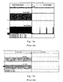
- FIGS. 13 a - b show experimental results of an output voltage, buck pulses and boost pulses in a direct transition from buck mode to boost mode;
- FIGS. 14 a - b show experimental results of an output voltage, buck pulses and boost pulses in direct transition from buck mode to buck-boost mode
- FIGS. 15 a - b show experimental results of an output voltage, buck pulses and boost pulses in direct transition from buck-boost mode to boost mode;
- FIG. 16 shows an input voltage and an output voltage for the transition from buck to boost mode according to one embodiment of this invention
- FIGS. 17 a - f show experimental results for transitions from buck mode to a first combination mode to buck-boost mode to a second combination mode to boost mode according to one embodiment of this invention
- FIG. 18 shows experimental results for a transition from a first combination mode to a second combination mode for one embodiment of this invention.
- FIGS. 19 a - c shows three graphs of efficiency versus input voltage for three methods of operating the converter.
- This invention provides a method of controlling a converter to provide an output voltage from a variable input voltage.
- the invention reduces output voltage spikes during transitions from one mode to another mode by incorporating intermediate combination modes in place of direct transitions from one mode to another mode.
- converter 10 is provided with input voltage 12 and provides output voltage 14 .
- Input voltage 12 is a variable voltage source, such as a battery, that has a fully-charged voltage that drains to a drained voltage.
- Converter 10 functions to regulate input voltage 12 to a desired output voltage 14 .
- Converter 10 can be any type of converter including, but not limited to a positive buck-boost converter, an inverting buck-boost converter, a cascaded buck and boost converter, a ⁇ uk converter, a SEPIC converter or a fly-back converter.
- converter 10 should have the capability of operating in various converter topologies through controlled switching of components of the circuit.
- Controller 16 implements a control strategy of this invention.
- Controller 16 includes a converter topology control (CTC) 18 and at least one transition control (TC) unit 20 .
- the CTC 18 controls operating topologies of the converter 10 .
- the TC unit 20 controls transitions between various topologies.
- the controller 16 provides a drive signal and a switching frequency to the converter 10 .
- controller 16 comprises a pulse width modulation (PWM) controller.
- PWM pulse width modulation
- controller 16 includes a pulse circuit, which can be a monostable multivibrator.
- the monostable multivibrator also commonly known as a “one-shot,” is triggered, in one embodiment, by a rising edge of the drive signal to generate a pulse of fixed duration.
- the monostable vibrator may be triggered by a trailing edge of the drive signal.
- FIG. 3 shows a block diagram of one embodiment of the control strategy of this invention.
- the control strategy includes implementing first converting mode 22 , second converting mode 24 , third converting mode 26 , fourth converting mode 28 and fifth converting mode 30 .
- the control strategy can comprise any number or combination of converting modes according to this invention.
- FIG. 4 is a graph of voltage versus time illustrating the control strategy of FIG. 3 for a device with a variable input voltage 32 and a regulated output voltage 34 .
- converter 10 when input voltage 32 is higher than first predetermined voltage level 36 , converter 10 operates in first converting mode 22 .
- First converting mode 22 repeats a first duty cycle pulse for each period.
- second converting mode 24 When input voltage 32 is less than second predetermined voltage level 38 , converter 10 operates in second converting mode 24 .
- Second converting mode 24 repeats a second duty cycle pulse for each period.
- the converter When input voltage 32 has a value that is between first predetermined voltage level 36 and second predetermined voltage level 38 the converter operates in one or more combination modes.
- third converting mode 26 operates between first predetermined voltage level 36 and third predetermined voltage level 40 .
- Fourth converting mode 28 operates between fourth predetermined voltage level 42 and second predetermined voltage level 38 .
- fifth converting mode 30 operates between third predetermined voltage level 40 and fourth predetermined voltage level 42 .
- Converter 10 operates in third converting mode when input voltage 32 is equal to or less than first predetermined voltage level 36 and greater than third predetermined voltage level 40 .
- Third converting mode 26 comprises a combination configuration of the first duty cycle pulse for ⁇ i periods and the second duty pulse for ⁇ i periods, where ⁇ i and ⁇ i are positive integers.
- the combination configuration is repeated until input voltage 32 equals third predetermined voltage level 40 .
- the combination configuration can repeat a predetermined number of times ( ⁇ i ) and then controller 16 changes the operation of converter 10 to another converting mode.
- controller 16 operates converter 10 in fifth converting mode 30 .
- fifth converting mode 30 is not a combination mode, as it does not include a combination of the first duty cycle pulse and the second duty cycle pulse.
- Fifth converting mode 30 comprises a third duty cycle pulse which is different from the first duty cycle pulse and the second duty cycle pulse.
- Fifth converting mode 30 can be a buck-boost mode.
- Fourth converting mode 28 comprises a second combination configuration of the second duty pulse for ⁇ n periods and the first duty cycle pulse for ⁇ n periods, where ⁇ n and ⁇ n are positive integers.
- the second combination configuration repeats until input voltage 12 equals second predetermined voltage level 38 .
- the second combination configuration can repeat a predetermined number of times ( ⁇ n ) and then controller 16 changes the operation of converter 10 to another converting mode.
- control strategy includes first converting mode 22 , second converting mode 24 , third converting mode 26 and fourth converting mode 28 .
- fifth converting mode 30 can be eliminated because implementing fifth converting mode 30 often leads to an undesirable higher loss that decreases the efficiency of converter 10 .
- FIG. 5 shows an alternative control strategy of this invention, including three modes.
- the control strategy of FIG. 5 includes first converting mode 52 , second converting mode 54 and third converting mode 56 .
- FIG. 6 is a graph of voltage versus time for a device with a variable input voltage 62 and a regulated output voltage 64 and illustrating the control strategy of FIG. 5 .
- first converting mode 52 when input voltage 62 is higher than first predetermined voltage level 66 , converter 10 operates in first converting mode 52 .
- First converting mode 52 repeats the first duty cycle pulse for each period.
- second converting mode 54 when input voltage 62 is less than second predetermined voltage level 68 , converter 10 operates in second converting mode 54 .
- Second converting mode 54 repeats the second duty cycle pulse for each period.
- Third converting mode 56 comes into operation when input voltage 62 is equal to or less than first predetermined voltage level 66 and greater than second predetermined voltage level 68 .
- Third converting mode 56 comprises a plurality of sequential combination configurations of the first duty cycle pulse and the second duty cycle pulse.
- a first sequential combination comprises a plurality of the first duty cycle pulse ( ⁇ first duty cycle pulses) followed by at least one second duty cycle pulse ( ⁇ second duty cycle pulses).
- a second sequential combination comprises a lesser amount (x) than the plurality of the first duty cycle pulse ( ⁇ x) and an increased amount of the second duty cycle pulse ( ⁇ +x).
- the sequential combination configuration can continue until only a set number of the first duty cycle pulses, generally one, remain.
- the pattern would be: 6,1; 5,2; 4,3; 3,4; 2,5; 1,6.
- Alternatives include changing each sequential combination by two or another integer less than ⁇ .
- positive buck-boost converter 70 comprises input voltage 72 , first switching device 74 , first diode 76 , inductive device 78 , second switching device 80 , second diode 82 , capacitor 84 and output voltage 86 .
- Positive buck-boost converter 70 is connected to controller 88 , first gate driver 90 and second gate driver 92 .
- first converting mode 22 can be a buck mode
- second converting mode 24 can be a boost mode
- fifth converting mode 30 can be a buck-boost mode.
- third converting mode 26 and fourth converting mode 28 are combination modes.
- Positive buck-boost converter 70 can operate in the buck-boost mode by switching on, i.e., conducting, first switching device 74 and second switching device 80 for the buck-boost duty cycle and then off, i.e., not conducting, for the remainder of a period.
- Converter 70 can operate in the buck mode by keeping second switching device 80 off and switching first switching device 74 on for a buck duty cycle and off for the remainder of the period.
- Converter 70 can operate in the boost mode by keeping first switching device 74 on and switching second switching device 80 on for a boost duty cycle and off for the remainder of the period.
- the number of first duty cycle pulses ( ⁇ i ) and the number of second duty cycle pulses ( ⁇ i ) must be determined.
- An analytical approach can be used to calculate the ⁇ i first duty cycle pulses and the ⁇ i second duty cycle pulses, where the first duty cycle pulses are buck pulses and the second duty cycle pulses are boost pulses.
- the output voltage variation can be expressed as:
- A 1 C ⁇ ( ⁇ 1 + ⁇ 1 ) ⁇ ( ⁇ 1 ⁇ ( v i ⁇ ⁇ n - v out 2 ⁇ L ⁇ d buck ⁇ T + I 0 , buck - 1 R ⁇ v out ) + ⁇ 1 ⁇ ( ( 1 - d boost ) ⁇ v i ⁇ ⁇ n 2 ⁇ L ⁇ d boost ⁇ T + I 0 , boost - 1 R ⁇ v out ) ) . ( 5 ) Since the desired output voltage variation, i.e. voltage ripple/voltage spike, is minimum or zero,
- A can be set to zero to solve for ⁇ 1 / ⁇ 1 :
- ⁇ 1 ⁇ 1 - ( 1 - d boost ) 2 ⁇ v out 2 ⁇ L ⁇ d boost ⁇ T - I 0 , boost + 1 R ⁇ v out ( 1 - d buck ) ⁇ v out 2 ⁇ L ⁇ T + I 0 , buck - 1 R ⁇ v out . ( 6 )
- the ratio of boost and buck pulses can be defined in terms of circuit parameters.
- a trial and error approach can be used to determine the ⁇ first duty cycle pulse and the ⁇ second duty cycle pulse in third converting mode 26 and/or fourth converting mode 28 .
- FIGS. 8-12 are graphs of simulation results for four methods of controlling positive buck-boost converter 70 , two prior art methods and two methods according to this invention.
- FIGS. 13-18 are graphs of experimental results, which confirm the simulations. All simulations and experimental results are based the parameters provided in Table 1.
- FIG. 8 presents an input voltage waveform, an output voltage waveform, buck pulses and boost pulses for a direct transition from buck mode to boost mode.
- the simulation results indicate the presence of a 12% to 14% voltage spike in the output voltage during direct transition from buck mode to boost mode.
- FIG. 9 presents an output voltage waveform, an input voltage, and buck and boost pulses for a transition from buck mode to buck-boost mode to boost mode.
- the converter initially works in buck mode, when the input voltage is greater than the output voltage, followed by buck-boost mode when the voltages are almost equal. Finally the converter works in boost mode when the input voltage is lower than the output voltage.
- the simulation results indicate about a 6% voltage spike in the output voltage during transitions.
- the first combination mode and the second combination mode comprise an embodiment of this invention with a repeating (not sequential) combination of buck and boost pulses.
- Equation (6) just before ⁇ in ⁇ out , to calculate ⁇ 1 / ⁇ 1 for the first combination mode provides a ratio of 3:1. Just after ⁇ in ⁇ out , calculating ⁇ 2 / ⁇ 2 for the second combination mode provides a ratio of 1:2.
- the simulation uses three buck pulses and one boost pulse for the first combination mode and one buck pulse and two boost pulses for the second combination mode.
- A refer to the first combination mode, while the references to Comb. B or Comb. mode B refer to the second combination mode.
- FIG. 10 presents an output voltage waveform, an input voltage waveform, buck pulses and boost pulses for transitions from buck mode to the first combination mode to buck-boost mode to the second combination mode to boost mode.
- the simulation results indicate about a 4% voltage spike in the output voltage during transitions through the different modes. This method thus improves the ripple in the output voltage of the converter during transients.
- FIG. 11 presents an output voltage waveform, an input voltage waveform, buck pulses and boost pulses for transitions from buck mode to the first combination mode to the second combination mode to boost mode.
- the simulation results indicate about a 4% voltage spike in the output voltage during transitions through the different modes. This result is roughly the same as the method with the buck-boost mode in the middle ( FIG. 10 ).
- operating the converter in the buck-boost mode decreases the efficiency of the converter, eliminating the buck-boost mode significantly improves the efficiency of the converter.
- FIG. 12 presents the output voltages from the simulations of all four transition methods for comparison.
- First switching device 74 and second switching device 80 were N-type MOSFET switches, model number IRF540.
- First diode 76 and second diode 82 were Schottky barrier diodes, model number 1N5817.
- Controller 88 included a Texas Instrument Digital Signal Processor (DSP), model number 320F2812.
- DSP Texas Instrument Digital Signal Processor
- Two high-side gate drivers 90 , 92 and dedicated gating logic configure converter 70 into buck mode, buck-boost mode and boost mode. High-side gate drivers 90 , 92 were dependent on mode selection signals from the DSP.
- FIG. 13 a shows the experimental results of the waveforms for output voltage, buck mode pulses and boost mode pulses in direct transition from buck mode to boost mode.
- FIG. 13 b shows a closer view of the waveforms.
- FIGS. 13 a - b show a voltage spike in the output voltage during the transition from buck mode to boost mode.
- FIGS. 14 a - b and 15 a - b show the experimental results of the waveforms for output voltage, buck mode pulses, boost mode pulses, and buck-boost mode pulses for a direct transition from buck to buck-boost mode and from buck-boost mode to boost mode, also with closer views of the waveforms for each transition.
- the first combination mode and the second combination mode comprise an embodiment of this invention with a repeating (not sequential) combination of buck and boost pulses.
- FIG. 16 presents the input voltage and the output voltage for the transition from buck to the first combination mode to the second combination mode to boost mode.
- the input voltage decreases from 6 V to 3.6 V while the output voltage is tightly regulated at 5 V.
- FIGS. 17 a - f The experimental result for the transition from buck mode to the first combination mode to buck-boost mode to buck-boost mode to the second combination mode to boost mode is shown in detail in FIGS. 17 a - f .
- FIG. 17 a shows the output voltage variation as well as buck and boost pulses in transition from the buck mode to the first combination mode.
- FIG. 17 b shows buck and boost pulses in the first combination mode, where three buck pulses are associated with one boost pulse.
- FIG. 17 c shows buck, boost, and buck-boost pulses in the transition from the first combination mode to the buck-boost mode.
- FIG. 17 a shows the output voltage variation as well as buck and boost pulses in transition from the buck mode to the first combination mode.
- FIG. 17 b shows buck and boost pulses in the first combination mode, where three buck pulses are associated with one boost pulse.
- FIG. 17 c shows buck, boost, and
- FIG. 17 d shows buck, boost, and buck-boost pulses in the transition from the buck-boost mode to the second combination mode.
- FIG. 17 e shows buck and boost pulses in the second combination mode, before transition to the boost mode. In the second combination mode, each buck pulse is associated with two boost pulses.
- FIG. 17 f shows the output voltage, the buck pulses and the boost pulses in the transition from the second combination mode to the boost mode.
- FIG. 18 shows the experimental results for the output voltage, buck pulses, and boost pulses in a direct transition from the first combination mode to the second combination mode for an embodiment of this invention where the buck-boost mode is omitted.
- Table 2 summarizes experimental results of the output voltage ripple during transitions from different modes of operation.
- the voltage ripple is defined as the peak-peak ripple as a percentage of the output voltage of the converter.
- Direct transition from buck to boost has a voltage ripple of about 12% ( FIG. 13 ).
- the addition of the buck-boost mode improves the voltage ripple to about 4% in transition from buck to buck-boost ( FIG. 14 ) and improves the voltage ripple of transition from buck-boost to boost to about 6% ( FIG. 15 ); however, staying in the buck-boost mode for a long time sacrifices the efficiency of the converter.
- Adding the first combination mode and the second combination mode between buck and boost modes significantly improves the voltage ripple to less than 2-3% ( FIGS. 16-18 ).
- FIGS. 19 a - c present efficiency (P out /P in ) versus the input voltage for three methods of operating the converter for three loads (R) at the output voltage.
- Efficiency is a function of a load profile. Increasing the load power decreases the efficiency because of increases of ohmic and switching losses.
- FIG. 19 b presents the efficiency of the converter in the transition from buck mode to first combination mode to buck-boost mode. Similar to the results of FIG.
- the invention provides a method for controlling a DC/DC converter with a variable power supply.
- the method introduced improves the dynamic response of the converter during transients by switching between different converter topologies to spread out voltage spikes, which are an inevitable result of transients.
- the invention also can improve the efficiency of the DC/DC converter by replacing higher loss modes with combination modes.
Landscapes
- Engineering & Computer Science (AREA)
- Power Engineering (AREA)
- Dc-Dc Converters (AREA)
Abstract
Description
will approach 1. In the boost mode, when the input voltage (Vin) approaches the output voltage (Vout), a boost duty cycle,
moves toward zero. In the buck-boost mode, when the input voltage (Vin) equal to the output voltage (Vout) a buck-boost duty cycle,
becomes 0.5. As the fully-charged voltage (VinH) decreases towards the discharged voltage (VinL), the duty cycle should follow the pattern of 1 for the buck mode to 0.5 for the buck-boost mode and then to 0 in the boost mode. Output voltage spikes are associated with these sudden changes in the duty cycle.
I0,boost represent initial currents of
Since the desired output voltage variation, i.e. voltage ripple/voltage spike, is minimum or zero,
can be set to zero to solve for α1/β1:
| TABLE 1 | ||||
| Variable | Parameter | | ||
| L | inductance | |||
| 100 μH | ||||
| C | Output filter capacitance | 330 μF | ||
| Vin | Input voltage | 3.6 V-6 V | ||
| Vref | Output voltage | 5 V | ||
| | Switching frequency | 100 kHz | ||
| | Output resistance | 20 Ω | ||
Simulation Results of the Prior Art, Direct Transition Method:
| TABLE 2 | |
| Output voltage | |
| Transition | ripple (%) |
| Direct buck to boost | 12% |
| Buck to buck- |
4% |
| Buck-boost to boost | 6% |
| Buck to first combination mode | <3% |
| First combination mode to buck-boost | <2% |
| Buck-boost to second combination mode | <2% |
| Second combination mode to boost | <3% |
| First combination mode to second combination mode | <2% |
Claims (12)
Priority Applications (1)
| Application Number | Priority Date | Filing Date | Title |
|---|---|---|---|
| US12/337,211 US8089254B2 (en) | 2008-12-17 | 2008-12-17 | Digital control of power converters |
Applications Claiming Priority (1)
| Application Number | Priority Date | Filing Date | Title |
|---|---|---|---|
| US12/337,211 US8089254B2 (en) | 2008-12-17 | 2008-12-17 | Digital control of power converters |
Publications (2)
| Publication Number | Publication Date |
|---|---|
| US20100148739A1 US20100148739A1 (en) | 2010-06-17 |
| US8089254B2 true US8089254B2 (en) | 2012-01-03 |
Family
ID=42239711
Family Applications (1)
| Application Number | Title | Priority Date | Filing Date |
|---|---|---|---|
| US12/337,211 Expired - Fee Related US8089254B2 (en) | 2008-12-17 | 2008-12-17 | Digital control of power converters |
Country Status (1)
| Country | Link |
|---|---|
| US (1) | US8089254B2 (en) |
Cited By (2)
| Publication number | Priority date | Publication date | Assignee | Title |
|---|---|---|---|---|
| US20180235046A1 (en) * | 2017-02-16 | 2018-08-16 | Muyshondt Enterprises, Inc. | Apparatus For Controlling Multiple Electrical Loads Using a Multi-Driver/Multi-Topology Regulator Design |
| US20240030821A1 (en) * | 2022-07-25 | 2024-01-25 | P-Duke Technology Co., Ltd. | Novel power supply apparatus |
Families Citing this family (9)
| Publication number | Priority date | Publication date | Assignee | Title |
|---|---|---|---|---|
| US8354827B2 (en) * | 2009-06-03 | 2013-01-15 | Lincoln Global, Inc. | Controller for a buck-boost circuit |
| TW201251289A (en) * | 2011-06-07 | 2012-12-16 | Delta Electronics Inc | Integrated buck/boost converter of charging apparatus |
| IL217263B (en) * | 2011-12-29 | 2018-01-31 | Elta Systems Ltd | System, method and computer program product for controlling electric power supply |
| DE102012107442A1 (en) * | 2012-08-14 | 2014-05-15 | Hella Kgaa Hueck & Co. | Control unit for a step-up and down converter |
| US9878635B1 (en) * | 2013-02-13 | 2018-01-30 | University Of Maryland | Powertrain system in plug-in electric vehicles |
| US9419522B1 (en) * | 2013-02-13 | 2016-08-16 | University Of Maryland | ZVS DC/DC converter for converting voltage between a battery and a DC link in a hybrid energy storage system and method thereof |
| CN103595240A (en) * | 2013-11-20 | 2014-02-19 | 天津大学 | Device and method for reducing boosting amplitude of Boost type PFC converter |
| JP6962233B2 (en) * | 2018-02-22 | 2021-11-05 | 株式会社オートネットワーク技術研究所 | In-vehicle DCDC converter |
| CN113890343A (en) * | 2021-09-14 | 2022-01-04 | 宁波吉利罗佑发动机零部件有限公司 | Control method, device and system of boost converter and readable storage medium |
Citations (27)
| Publication number | Priority date | Publication date | Assignee | Title |
|---|---|---|---|---|
| US4039925A (en) | 1976-06-10 | 1977-08-02 | Nasa | Phase substitution of spare converter for a failed one of parallel phase staggered converters |
| US4115860A (en) | 1977-06-02 | 1978-09-19 | Lockheed Electronics Co., Inc. | Plural load power controller with time-shared processor |
| US4245286A (en) | 1979-05-21 | 1981-01-13 | The United States Of America As Represented By The Administrator Of The National Aeronautics And Space Administration | Buck/boost regulator |
| EP0207096A1 (en) | 1984-12-26 | 1987-01-07 | Hughes Aircraft Co | Power supply with volt-seconds sensing. |
| US4736151A (en) | 1986-12-23 | 1988-04-05 | Sundstrand Corporation | Bi-directional buck/boost DC/DC converter |
| US5371666A (en) | 1992-12-04 | 1994-12-06 | Square D Company | Average current mode control apparatus for an AC output amplifier |
| US5465011A (en) | 1992-12-14 | 1995-11-07 | Square D Company | Uninterruptible power supply with improved output regulation |
| US5831418A (en) * | 1996-12-03 | 1998-11-03 | Fujitsu Ltd. | Step-up/down DC-to-DC converter |
| US6037755A (en) | 1998-07-07 | 2000-03-14 | Lucent Technologies Inc. | Switching controller for a buck+boost converter and method of operation thereof |
| US6166527A (en) | 2000-03-27 | 2000-12-26 | Linear Technology Corporation | Control circuit and method for maintaining high efficiency in a buck-boost switching regulator |
| US6169680B1 (en) | 1996-06-24 | 2001-01-02 | Tdk Corporation | Switching power source with a digital control circuit to maintain a constant DC output signal |
| US6229288B1 (en) | 1995-01-11 | 2001-05-08 | Microplanet Ltd. | Method and apparatus for electronic power control |
| US20010043050A1 (en) | 1998-08-07 | 2001-11-22 | Carl Fisher | Apparatus and method for initial charging, self-starting, and operation of a power supply with an intermittent and/or variable energy source and a rechargeable energy storage device |
| EP1166430A1 (en) | 1999-03-31 | 2002-01-02 | Vari-Lite, Inc. | Universal power module |
| US6373150B1 (en) | 2000-03-14 | 2002-04-16 | Warren Electric Cooperative, Inc. | Electric service load limiter |
| EP1324476A1 (en) | 2001-12-27 | 2003-07-02 | Dialog Semiconductor GmbH | Converter with inductor and digital controlled timing |
| US20040027003A1 (en) | 2002-08-08 | 2004-02-12 | Tai-Her Yang | Multi-output device with preset power supply priority |
| US20040150928A1 (en) | 2003-02-03 | 2004-08-05 | Goodfellow John Ryan | Digitally controlled voltage regulator |
| US20040189271A1 (en) | 2002-04-29 | 2004-09-30 | Anders Hansson | Power supply system and apparatus |
| US20050002208A1 (en) | 2003-07-01 | 2005-01-06 | Shao-Tsu Kung | Power supply for outputting a steady state voltage according to a load requirement |
| EP1513239A1 (en) | 2002-03-22 | 2005-03-09 | Tai-Her Yang | Automatic charging system for an auxiliary battery |
| US20050254266A1 (en) * | 2002-03-29 | 2005-11-17 | Jitaru Ionel D | Method and apparatus for controlling a synchronous rectifier |
| US7102334B2 (en) | 1995-01-11 | 2006-09-05 | Microplanet Ltd. | Method and apparatus for electronic power control |
| US20080082277A1 (en) | 2006-09-28 | 2008-04-03 | Holmquist Gunnar R | AC output power supply with digital feedback loop |
| US20080218104A1 (en) | 2007-03-09 | 2008-09-11 | Srdjan Lukic | Power management for multi-module energy storage systems in electric, hybrid electric, and fuel cell vehicles |
| US20090039852A1 (en) * | 2007-08-06 | 2009-02-12 | Solaredge Technologies Ltd. | Digital average input current control in power converter |
| US20090103341A1 (en) | 2007-10-19 | 2009-04-23 | Young Joo Lee | Integrated bi-directional converter for plug-in hybrid electric vehicles |
Family Cites Families (1)
| Publication number | Priority date | Publication date | Assignee | Title |
|---|---|---|---|---|
| US20040043050A1 (en) * | 2002-09-03 | 2004-03-04 | Paulson Christopher Robert | Bot remover |
-
2008
- 2008-12-17 US US12/337,211 patent/US8089254B2/en not_active Expired - Fee Related
Patent Citations (27)
| Publication number | Priority date | Publication date | Assignee | Title |
|---|---|---|---|---|
| US4039925A (en) | 1976-06-10 | 1977-08-02 | Nasa | Phase substitution of spare converter for a failed one of parallel phase staggered converters |
| US4115860A (en) | 1977-06-02 | 1978-09-19 | Lockheed Electronics Co., Inc. | Plural load power controller with time-shared processor |
| US4245286A (en) | 1979-05-21 | 1981-01-13 | The United States Of America As Represented By The Administrator Of The National Aeronautics And Space Administration | Buck/boost regulator |
| EP0207096A1 (en) | 1984-12-26 | 1987-01-07 | Hughes Aircraft Co | Power supply with volt-seconds sensing. |
| US4736151A (en) | 1986-12-23 | 1988-04-05 | Sundstrand Corporation | Bi-directional buck/boost DC/DC converter |
| US5371666A (en) | 1992-12-04 | 1994-12-06 | Square D Company | Average current mode control apparatus for an AC output amplifier |
| US5465011A (en) | 1992-12-14 | 1995-11-07 | Square D Company | Uninterruptible power supply with improved output regulation |
| US7102334B2 (en) | 1995-01-11 | 2006-09-05 | Microplanet Ltd. | Method and apparatus for electronic power control |
| US6229288B1 (en) | 1995-01-11 | 2001-05-08 | Microplanet Ltd. | Method and apparatus for electronic power control |
| US6169680B1 (en) | 1996-06-24 | 2001-01-02 | Tdk Corporation | Switching power source with a digital control circuit to maintain a constant DC output signal |
| US5831418A (en) * | 1996-12-03 | 1998-11-03 | Fujitsu Ltd. | Step-up/down DC-to-DC converter |
| US6037755A (en) | 1998-07-07 | 2000-03-14 | Lucent Technologies Inc. | Switching controller for a buck+boost converter and method of operation thereof |
| US20010043050A1 (en) | 1998-08-07 | 2001-11-22 | Carl Fisher | Apparatus and method for initial charging, self-starting, and operation of a power supply with an intermittent and/or variable energy source and a rechargeable energy storage device |
| EP1166430A1 (en) | 1999-03-31 | 2002-01-02 | Vari-Lite, Inc. | Universal power module |
| US6373150B1 (en) | 2000-03-14 | 2002-04-16 | Warren Electric Cooperative, Inc. | Electric service load limiter |
| US6166527A (en) | 2000-03-27 | 2000-12-26 | Linear Technology Corporation | Control circuit and method for maintaining high efficiency in a buck-boost switching regulator |
| EP1324476A1 (en) | 2001-12-27 | 2003-07-02 | Dialog Semiconductor GmbH | Converter with inductor and digital controlled timing |
| EP1513239A1 (en) | 2002-03-22 | 2005-03-09 | Tai-Her Yang | Automatic charging system for an auxiliary battery |
| US20050254266A1 (en) * | 2002-03-29 | 2005-11-17 | Jitaru Ionel D | Method and apparatus for controlling a synchronous rectifier |
| US20040189271A1 (en) | 2002-04-29 | 2004-09-30 | Anders Hansson | Power supply system and apparatus |
| US20040027003A1 (en) | 2002-08-08 | 2004-02-12 | Tai-Her Yang | Multi-output device with preset power supply priority |
| US20040150928A1 (en) | 2003-02-03 | 2004-08-05 | Goodfellow John Ryan | Digitally controlled voltage regulator |
| US20050002208A1 (en) | 2003-07-01 | 2005-01-06 | Shao-Tsu Kung | Power supply for outputting a steady state voltage according to a load requirement |
| US20080082277A1 (en) | 2006-09-28 | 2008-04-03 | Holmquist Gunnar R | AC output power supply with digital feedback loop |
| US20080218104A1 (en) | 2007-03-09 | 2008-09-11 | Srdjan Lukic | Power management for multi-module energy storage systems in electric, hybrid electric, and fuel cell vehicles |
| US20090039852A1 (en) * | 2007-08-06 | 2009-02-12 | Solaredge Technologies Ltd. | Digital average input current control in power converter |
| US20090103341A1 (en) | 2007-10-19 | 2009-04-23 | Young Joo Lee | Integrated bi-directional converter for plug-in hybrid electric vehicles |
Non-Patent Citations (22)
| Title |
|---|
| A. Chakraborty et al., "Combination of Buck and Boost Modes to Minimize Transients in the Output of a Positive Buck-Boost Converter," Proc. IEEE 32nd Industrial Electronics Annual Conference, Paris, France, Nov. 2006, pp. 2372-2377. |
| A. Chakraborty et al., "Digital Combination of Buck and Boost Converters to Control a Positive Buck-Boost Converter," Proc. IEEE Power Electronics Specialists Conference, Jun. 2006, vol. 1, pp. 1-6. |
| A. Chakraborty, Digital Combination of DC/DC Converter: A Novel Theory Applied to Positive Buck-Boost Converters, May 2007, Illinois Institute of Technology, 1-170. * |
| A. Rahimi et al., "Sub-Harmonic Problem in Multi-Converter Vehicular Power Systems," Proc. IEEE Vehicular Power and Propulsion Conference, Windsor, U.K., Sep. 2006, 5 pages. |
| A. Syed et al., "Digital PWM Controller with Feed-Forward Compensation," Proc. IEEE Applied Power Electronics Conference and Expo, Sep. 2004, vol. 1, pp. 60-66. |
| B. Bryant et al., "Derivation of the buck-boost PWM DC-DC Converter Circuit Topology," Proc. International Symposium on Circuits and Systems, May 2002, vol. 5, pp. 841-844. |
| B. Sahu et al., "A Low Voltage, Dynamic, Noninverting, Synchronous Buck-Boost Converter for Portable Applications," IEEE Transactions on Power Elect., Mar. 2004, vol. 19, No. 2, pp. 443-452. |
| Chakraborty et al., Digital Combitation of buck and Boost Modes to Control a Positive Buck-Boost Converter, IEEE, Jun. 2006, PESC '06 37th IEEE, 2372-2377, 1-6. * |
| Co-pending U.S. Appl. No. 12/337,129, filed Dec. 17, 2008. |
| D. Adar et al., "A Unified Behavioral Average Model of Sepic Converters with Coupled Inductors," Proc. IEEE Power Elect. Specialists Conference, Jun. 1997, vol. 1, pp. 441-446. |
| J. Chen et al., "Buck-Boost PWM Converters Having Two Independently Controlled Switches," Proc. IEEE 32nd Power Elect. Specialists Conf., Jun. 2001, vol. 2, pp. 736-741. |
| L. Yang et al., "Analysis and Design of a Novel Three-Phase AC-DC Buck-Boost Converter," IEEE Transactions on Power Electronics, Mar. 2008, vol. 23, pp. 707-714. |
| M. Gaboriault et al., "A High Efficiency, Non-Inverting, Buck-Boost DC-DC Converter," Proc. IEEE Applied Power Electronics Conference, Sep. 2004, vol. 3, pp. 1411-1415. |
| R.S. Weissbach et al., "A Noninverting Buck-Boost Converter with Reduced Components using a Microcontroller," Proc. IEEE Southeast Conference, Apr. 2001, vol. 2, pp. 79-84. |
| US 5,780,998, 07/1998, Scott et al. (withdrawn) |
| V.D. Yurkevich, "Design of Controller for Buck-Boost Converter," Proc. Science and Technology, Jun. 2005, pp. 741-745. |
| W.M. Moussa, "Modeling and Performance Evaluation of a DC/DC Sepic Converter," Proc. IEEE Applied Power Electronics Conference, Mar. 1995, vol. 2, pp. 702-706. |
| X. Ren et al., "Four Switch Buck-Boost Converter for Telecom DC-DC Power Supply Applications," Proc. IEEE 23rd Applied Power Elect. Confr. and Expo, Feb. 2008, pp. 1527-1530. |
| Y. Konishi et al., "Soft-Switching Buck Boost Converter using Passive Snubber composed of Pulse Current Regenerative Resonant Circuit," Elect. Ltrs., Jan. 2007, vol. 43, pp. 886-890. |
| Y. Lee et al., "Digital Combination of Buck and Boost Converters to Control a Positive Buck-Boost Converter and Improve the Output Transients," submitted to IEEE Transactions on Power Electronics on May 28, 2008, 34 pages. |
| Y.Zhang et al., "A New Soft Switching Technique for Buck, Boost and Buck-Boost Converters," IEEE Transactions on Industry Applications, Nov. 2003, vol. 39, No. 6, pp. 2343-2350. |
| Z. Shameem, "Discrete Circuit Protects Li-Ion Battery Charger," Proc. Power Electronics Technology Magazine, Mar. 2007, pp. 50-51. |
Cited By (3)
| Publication number | Priority date | Publication date | Assignee | Title |
|---|---|---|---|---|
| US20180235046A1 (en) * | 2017-02-16 | 2018-08-16 | Muyshondt Enterprises, Inc. | Apparatus For Controlling Multiple Electrical Loads Using a Multi-Driver/Multi-Topology Regulator Design |
| US10285233B2 (en) * | 2017-02-16 | 2019-05-07 | Muyshondt Enterprises, Inc. | Apparatus for controlling multiple electrical loads using a multi-driver/multi-topology regulator design |
| US20240030821A1 (en) * | 2022-07-25 | 2024-01-25 | P-Duke Technology Co., Ltd. | Novel power supply apparatus |
Also Published As
| Publication number | Publication date |
|---|---|
| US20100148739A1 (en) | 2010-06-17 |
Similar Documents
| Publication | Publication Date | Title |
|---|---|---|
| US8089254B2 (en) | Digital control of power converters | |
| US7304463B2 (en) | DC-DC converter | |
| US9246387B2 (en) | Output voltage controller, electronic device, and output voltage control method | |
| US8456143B2 (en) | DC-DC converter and semiconductor integrated circuit for controlling power source | |
| KR101324806B1 (en) | Boost and up-down switching regulator with synchronous freewheeling mosfet | |
| TWI536723B (en) | Efficient control circuit for buck-boost converters and control method thereof | |
| TWI406484B (en) | Time-multiplexed multi-output dc/dc converters and voltage regulators | |
| US11563378B2 (en) | Seamless DCM-PFM transition for single pulse operation in DC-DC converters | |
| US20110285369A1 (en) | Three-switch step-down converter | |
| US20090039711A1 (en) | Dual-Polarity Multi-Output DC/DC Converters and Voltage Regulators | |
| US20040201281A1 (en) | Single-inductor multiple-output switching converters in PCCM with freewheel switching | |
| US20110101946A1 (en) | Voltage converters | |
| US7456624B2 (en) | PWM control scheme under light load | |
| KR20100022959A (en) | Step-down switching regulator with freewheeling diode | |
| US20150015225A1 (en) | Multi-phase buck dc converter | |
| US20120306466A1 (en) | Step-up dc-dc converter | |
| US9608517B2 (en) | System and method to eliminate transition losses in DC/DC converters | |
| CN107404229B (en) | Method and apparatus for adaptive timing of zero voltage transition power converters | |
| US6825641B2 (en) | High efficiency electrical switch and DC-DC converter incorporating same | |
| Tattiwong et al. | Analysis design and experimental verification of a quadratic boost converter | |
| US20060049811A1 (en) | Output voltage ripple reduction technique for burst mode operation of power converter | |
| US10348205B1 (en) | Coupled-inductor cascaded buck converter with fast transient response | |
| CN110692185A (en) | DC voltage conversion device | |
| Guo et al. | A multi-modes charge-pump based high efficiency wide input range DC-DC converter | |
| KR101906311B1 (en) | Dc converter and method for controlling the same |
Legal Events
| Date | Code | Title | Description |
|---|---|---|---|
| AS | Assignment |
Owner name: ILLINOIS INSTITUTE OF TECHNOLOGY,ILLINOIS Free format text: ASSIGNMENT OF ASSIGNORS INTEREST;ASSIGNORS:KHALIGH, ALIREZA;LEE, YOUNG-JOO;EMADI, ALI;SIGNING DATES FROM 20081212 TO 20081214;REEL/FRAME:021996/0387 Owner name: ILLINOIS INSTITUTE OF TECHNOLOGY, ILLINOIS Free format text: ASSIGNMENT OF ASSIGNORS INTEREST;ASSIGNORS:KHALIGH, ALIREZA;LEE, YOUNG-JOO;EMADI, ALI;SIGNING DATES FROM 20081212 TO 20081214;REEL/FRAME:021996/0387 |
|
| ZAAA | Notice of allowance and fees due |
Free format text: ORIGINAL CODE: NOA |
|
| ZAAB | Notice of allowance mailed |
Free format text: ORIGINAL CODE: MN/=. |
|
| STCF | Information on status: patent grant |
Free format text: PATENTED CASE |
|
| REMI | Maintenance fee reminder mailed | ||
| FEPP | Fee payment procedure |
Free format text: PATENT HOLDER CLAIMS MICRO ENTITY STATUS, ENTITY STATUS SET TO MICRO (ORIGINAL EVENT CODE: STOM); ENTITY STATUS OF PATENT OWNER: SMALL ENTITY |
|
| FPAY | Fee payment |
Year of fee payment: 4 |
|
| SULP | Surcharge for late payment | ||
| AS | Assignment |
Owner name: SOFTWARE MOTOR CORPORATION, CALIFORNIA Free format text: ASSIGNMENT OF ASSIGNORS INTEREST;ASSIGNOR:MESON CONSTRUCTIVE CAPITAL LP;REEL/FRAME:044045/0145 Effective date: 20171106 Owner name: MESON CONSTRUCTIVE CAPITAL LP, CALIFORNIA Free format text: ASSIGNMENT OF ASSIGNORS INTEREST;ASSIGNOR:ILLINOIS INSTITUTE OF TECHNOLOGY;REEL/FRAME:044384/0311 Effective date: 20171016 |
|
| AS | Assignment |
Owner name: SOFTWARE MOTOR COMPANY, CALIFORNIA Free format text: CHANGE OF NAME;ASSIGNOR:SOFTWARE MOTOR CORPORATION;REEL/FRAME:044975/0700 Effective date: 20171213 |
|
| MAFP | Maintenance fee payment |
Free format text: PAYMENT OF MAINTENANCE FEE, 8TH YR, SMALL ENTITY (ORIGINAL EVENT CODE: M2552); ENTITY STATUS OF PATENT OWNER: SMALL ENTITY Year of fee payment: 8 |
|
| AS | Assignment |
Owner name: TURNTIDE TECHNOLOGIES INC., CALIFORNIA Free format text: CHANGE OF NAME;ASSIGNOR:SOFTWARE MOTOR COMPANY;REEL/FRAME:053294/0848 Effective date: 20200720 |
|
| FEPP | Fee payment procedure |
Free format text: MAINTENANCE FEE REMINDER MAILED (ORIGINAL EVENT CODE: REM.); ENTITY STATUS OF PATENT OWNER: SMALL ENTITY |
|
| LAPS | Lapse for failure to pay maintenance fees |
Free format text: PATENT EXPIRED FOR FAILURE TO PAY MAINTENANCE FEES (ORIGINAL EVENT CODE: EXP.); ENTITY STATUS OF PATENT OWNER: SMALL ENTITY |
|
| STCH | Information on status: patent discontinuation |
Free format text: PATENT EXPIRED DUE TO NONPAYMENT OF MAINTENANCE FEES UNDER 37 CFR 1.362 |
|
| FP | Lapsed due to failure to pay maintenance fee |
Effective date: 20240103 |