US7710065B2 - Power conversion system and power conversion control method - Google Patents
Power conversion system and power conversion control method Download PDFInfo
- Publication number
- US7710065B2 US7710065B2 US11/876,971 US87697107A US7710065B2 US 7710065 B2 US7710065 B2 US 7710065B2 US 87697107 A US87697107 A US 87697107A US 7710065 B2 US7710065 B2 US 7710065B2
- Authority
- US
- United States
- Prior art keywords
- output voltage
- voltage command
- motor
- command value
- vector
- Prior art date
- Legal status (The legal status is an assumption and is not a legal conclusion. Google has not performed a legal analysis and makes no representation as to the accuracy of the status listed.)
- Active, expires
Links
Images


Classifications
-
- H—ELECTRICITY
- H02—GENERATION; CONVERSION OR DISTRIBUTION OF ELECTRIC POWER
- H02J—CIRCUIT ARRANGEMENTS OR SYSTEMS FOR SUPPLYING OR DISTRIBUTING ELECTRIC POWER; SYSTEMS FOR STORING ELECTRIC ENERGY
- H02J1/00—Circuit arrangements for dc mains or dc distribution networks
- H02J1/10—Parallel operation of dc sources
- H02J1/102—Parallel operation of dc sources being switching converters
-
- H—ELECTRICITY
- H02—GENERATION; CONVERSION OR DISTRIBUTION OF ELECTRIC POWER
- H02J—CIRCUIT ARRANGEMENTS OR SYSTEMS FOR SUPPLYING OR DISTRIBUTING ELECTRIC POWER; SYSTEMS FOR STORING ELECTRIC ENERGY
- H02J3/00—Circuit arrangements for ac mains or ac distribution networks
- H02J3/38—Arrangements for parallely feeding a single network by two or more generators, converters or transformers
Definitions
- the present invention relates to a power conversion system and a power conversion control method.
- Japanese Laid-Open Patent Application Publication No. 2006-33956 discloses an example of a known motor drive system control apparatus that uses a plurality of power sources that supply electric power to an electric motor and that controls the electric power supplied from each of the power sources to a desired value.
- a voltage command value applied to the motor is divided according to the ratio of the distribution target values of the electric power outputted from the power sources to produce a second voltage command value group.
- the voltage command value applied to the motor is divided into portions in accordance with the ratio indicated by the electric target power distribution values so as to produce a second voltage command value group. Consequently, particularly when power is transferred among the power sources, the power factors of the voltages outputted from the power sources will be poor if the power factors of the current and voltage supplied to the motor are poor. Under such conditions, a larger voltage is required in order to supply a given current, and thus, the efficiency declines.
- one object of the present invention is to provide a control method for a low-loss electric power converter that can control the electric power supplied from each of a plurality of power sources to a desired value and accomplish transferring of power among the power sources with a high degree of efficiency.
- a power conversion system includes a first voltage source, a second voltage source, a multiple-phase alternating current motor, a switch section and a control unit.
- the switch section is configured to produce an output pulse based on first and second output voltages of the first and second voltage sources, respectively, to drive the multiple-phase alternating current motor.
- the control unit is configured to control the switch section.
- the control unit includes a torque computing section, an output voltage command value computing section, and a PWM pulse generating section.
- the torque computing section is configured to compute a motor current command value and a motor voltage command value that satisfy a motor torque command value.
- the output voltage command value computing section is configured to compute first and second output voltage command values for the first and second voltage sources, respectively, that satisfy the motor current command value, the motor voltage command value and a target charged power that is set based on conditions of the first and second voltage sources.
- the PWM pulse generating section is configured to generate a PWM pulse for driving the switch section based on the first and second output voltage command values.
- the output voltage command value computing section of the control unit is further configured to compute the first and second output voltage command values based on a first output voltage command vector and a second output voltage command vector when the first voltage source is to be charged and the second voltage source is to be discharged.
- the first output voltage command vector corresponds to the first output voltage command value of the first voltage source satisfying the target charged power.
- the second output voltage command vector corresponds to the second output voltage command value of the second voltage source.
- the first and second output voltage command vectors are determined so that a resultant vector of the first and second output voltage command vectors is coincident with a motor voltage command vector corresponding to the motor voltage command value, and a motor current command vector corresponding to the motor current command value is positioned within an included angle formed between the second output voltage command vector and a negative vector of the first output voltage command vector.
- FIG. 1 is a circuit diagram of a power converter in accordance with a first embodiment of the present invention
- FIG. 2 is a functional block diagram of a power conversion control system in accordance with the first embodiment of the present invention
- FIG. 3 is a functional block diagram of a current/power control device in accordance with the first embodiment of the present invention.
- FIG. 4 is a flowchart for a revision voltage control executed by the power conversion control system in accordance with the first embodiment of the present invention
- FIG. 5 is a vector diagram illustrating the relationships of output voltage command values and current command values of the power sources in the first embodiment of the present invention
- FIG. 6 is a schematic diagram illustrating examples of the waveforms of the motor current and the output voltages of the power sources in accordance with the first embodiment of the present invention
- FIG. 7 is a schematic diagram illustrating examples of the waveforms of the motor current and the output voltages of the power sources in the case of a comparative example of a power conversion system
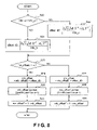
- FIG. 8 is a flowchart explaining the revision control of the modulation ratio executed by the power conversion control system in accordance with the first embodiment of the present invention.
- FIG. 9 is a schematic diagram illustrating the relationships of a revision modulation ratio, a modulation ratio, and the triangular waveform in accordance with the first embodiment of the present invention.
- FIG. 10 is a schematic diagram illustrating a triangular waveform used by a PWM pulse generating device in accordance with the first embodiment of the present invention.
- FIG. 11 is a partial schematic view of the circuit diagram illustrated in FIG. 1 showing only the circuit corresponding to the U-phase in accordance with the first embodiment of the present invention
- FIG. 12 is a schematic diagram illustrating how the pulse signals A and E are generated by comparing with the triangular waveform in accordance with the first embodiment of the present invention
- FIG. 13 is a schematic diagram illustrating how the pulse signals D and C are generated by comparing with the triangular waveform in accordance with the first embodiment of the present invention
- FIG. 14 is a schematic diagram illustrating an example of pulses generated with dead times being added in-between in accordance with the first embodiment of the present invention
- FIG. 15 is a functional block diagram illustrating a power conversion control system in accordance with a second embodiment of the present invention.
- FIG. 16 is a functional block diagram illustrating a current/power control device in accordance with the second embodiment of the present invention.
- FIG. 17 is a schematic diagram illustrating the relationships of output voltage command values and current command values of the power sources in accordance with the second embodiment of the present invention.
- FIG. 18 is a schematic diagram illustrating the relationships of the output voltage command values and the current command values of the power sources in accordance with the second embodiment of the present invention.
- FIG. 19 is a schematic diagram illustrating the relationships of the motor current and the output voltage command values of the power sources in accordance with the second embodiment of the present invention.
- FIG. 20 is a schematic diagram illustrating the relationships of the motor current and the output voltage command values of the power sources in accordance with the second embodiment of the present invention.
- FIG. 21 is a flowchart for a revision voltage control executed by the power conversion control system in accordance with a third embodiment of the present invention.
- FIG. 1 is a circuit diagram of a power converter 30 (switching section) used in a power conversion control system in accordance with the first embodiment of the present invention.
- the power converter 30 is electrically connected between a plurality of power sources 10 a and 10 b (first and second voltage sources) and a motor 20 .
- the motor 20 is preferably a well-known three-phase AC motor. More specifically, a negative electrode of the power source 10 a and a negative electrode of the power source 10 b are connected to a common negative bus bar 15 .
- a positive electrode of the power source 10 a is connected to a positive electrode bus bar 14 and a positive electrode of the power source 10 b is connected to a positive electrode bus bar 16 .
- the power source 10 b is, for example, a well-known secondary battery that can be selectively charged and discharged
- the power source 10 a is, for example, a well-known fuel cell that can be discharged.
- the present invention is not limited to this arrangement, however, and it is acceptable for the power source 10 a to be a secondary battery.
- the first embodiment of the present invention will be explained chiefly regarding a case in which the power source 10 b is charged with electric power from the power source 10 a (i.e., the electric power is transferred between the power sources 10 a and 10 b ).
- the illustrated embodiments are explained using an example where the power source 10 b is charged and the power source 10 a is discharged (i.e., the power source 10 b corresponds to the first voltage source to be charged and the power source 10 a corresponds to the second voltage source to be discharged in the present invention), it will be apparent to those skilled in the art from this disclosure that the charging/discharging arrangement of the power sources 10 a and 10 b are not limited to the arrangements described in the illustrated embodiments.
- the power sources 10 a and 10 b are both capable of charging and discharging electricity, either one of the power sources 10 a and 10 b can constitute the first voltage source to be charged in the present invention as long as the other one of the power sources 10 a and 10 b constitutes the second voltage source to be discharged.
- the power converter 30 includes component sets comprising semiconductor switches 107 a , 108 a and 109 a and diodes 107 b , 108 b and 109 b that are connected between the common negative bus bar 15 and the terminal for each phase of the motor 20 , similarly to a lower arm of a conventional inverter.
- a plurality of semiconductor switches 101 a / 101 b , 102 a / 102 b and 103 a / 103 b arranged to control current flow in both directions is connected between the positive electrode bus bar 14 of the power source 10 a and the terminal for each phase of the motor 20 .
- a plurality of semiconductor switches 104 a / 104 b , 105 a / 105 b and 106 a / 106 b arranged to control current flow in both directions is connected between the positive electrode bus bar 16 of the power source 10 b and the terminal for each phase of the motor 20 .
- a smoothing capacitor 12 is provided between the positive electrode bus bar 14 of the power source 10 a and the common negative electrode bus bar 15
- a smoothing capacitor 13 is provided between the positive electrode bus bar 16 of the power source 10 b and the common negative electrode bus bar 15 .
- the power converter 30 is a DC-AC power converting device configured and arranged to produce a voltage to be applied to the motor 20 based on the electric potentials of the common negative electrode bus bar 15 , the positive electrode bus bar 14 of the power source 10 a , and the positive electrode bus bar 16 of the power source 10 b .
- the semiconductor switches provided with respect to each of the phases U, V, and W of the motor 20 form three switch groups 30 U, 30 V and 30 W, respectively.
- the switch groups 30 U, 30 V and 30 W serve as switching device that produces voltages to be supplied to the phases of the motor 20 . More specifically, the required voltage is supplied to the motor 20 by selectively connecting one of these electric potentials at time and varying the time ratio at which the selected electric potential is connected by controlling the switch groups 30 U, 30 V and 30 W.
- the power conversion control system provided with the power converter 30 illustrated in FIG. 1 will be explained in accordance with the first embodiment of the present invention.
- the power converter 30 is operatively coupled to a controller 40 (control unit).
- the controller 40 preferably includes a microcomputer with a power conversion control program that controls the command values for the power sources 10 a and 10 b as discussed below.
- the controller 40 can also include other conventional components such as an input interface circuit, an output interface circuit, and storage devices such as a ROM (Read Only Memory) device and a RAM (Random Access Memory) device.
- the memory circuit stores processing results and control programs that are run by the processor circuit.
- the controller 40 is operatively coupled to the various components in a conventional manner.
- the internal RAM of the controller 40 stores statuses of operational flags and various control data.
- the internal ROM of the controller 40 stores the maps and data for various operations.
- the controller 40 is capable of selectively controlling any of the components of the control system in accordance with the control program.
- controller 40 can be any combination of hardware and software that will carry out the functions of the present invention.
- “means plus function” clauses as utilized in the specification and claims should include any structure or hardware and/or algorithm or software that can be utilized to carry out the function of the “means plus function” clause.
- the controller 40 constitutes a torque computing section including a torque control section 42 and a current control section 43 a ; an output voltage command value computing section including a revision voltage control section 43 b , a pair of multipliers 43 c 1 and 43 c 2 , a pair of adders 43 d 1 and 43 d 2 , and a pair of subtractors 43 e 1 and 43 e 2 ; a PWM pulse generating section including a modulation ratio computing section 45 , a modulation ratio revising section 46 , and a PWM pulse generating section 47 ; a minimum distributed power computing section and a comparing section including a comparator 41 of the present invention.
- the constituent features of the controller 40 will now be explained with reference to FIG. 2 .
- the controller 40 includes the comparator 41 , the torque control section 42 , a current/power control section 43 , the modulation ratio computing section 45 , the modulation ratio revising section 46 , the PWM pulse generating section 47 , and a three-phase/dq converting section 48 .
- the comparator 41 is configured to receive a torque command Te*, a motor rotational speed ⁇ , the voltage Vdc_a of the power source 10 a and the voltage Vdc_b of the power source 10 b from an external source of the controller 40 and to produce a minimum electric power command value Pmin (minimum distributed power) indicating the minimum electric power that can be received with distributed power control alone.
- the minimum electric power command value Pmin corresponds to a minimum electric power value distributed to the power source 10 a or 10 b according to power distribution control alone.
- the minimum electric power command value Pmin is a value lying within such a range that neither of the power source modulation ratios produced by the distributed power control exceeds 1 and is a value that can be received at a current value that allows the motor 20 to operate with good efficiency.
- the comparator 41 is also configured to receive an electric power command value Pb* of the power source 10 b .
- the electric power command value Pb* corresponds to a target charged power that is determined based on conditions of the power sources 10 a and 10 b and indicates the target power distributed between the power sources 10 a and 10 b .
- the minimum power command value Pmin and the electric power command value Pb* of the power source 10 b are compared in the comparator 41 to produce a comparison result Pcmpa*.
- the comparator 41 is configured to output the value 0 when the electric power command value Pb* is larger than the minimum power command value Pmin, and to output the value 1 when the electric power command value Pb* is smaller than the minimum power command value Pmin.
- the minimum electric power command value Pmin is a command value for the side that receives the electric power
- the minimum electric power command value Pmin is represented as a negative value.
- the minimum electric power command value Pmin indicates the maximum value in the negative direction.
- the electric power command value Pb* is on a positive side of the minimum electric power command value Pmin and the amount of regenerative charging power demanded is smaller than the amount of regenerative charging power that can be obtained with distributed power control.
- the electric power command value Pb* is smaller than the minimum electric power command value Pmin, then the electric power command value Pb* is on a negative side of the minimum electric power command value Pmin and the amount of regenerative charging power demanded is larger than the amount of regenerative charging power that can be obtained with distributed power control.
- the torque control section 42 is configured to compute a d-axis current command value id* of the AC motor 20 , a q-axis current command value iq* of the AC motor 20 , and a target power distribution value rto_pa based on the comparison result Pcmpa* and the torque command Te*, the motor rotational speed ⁇ , and the electric power command value Pb* of the power source 10 b obtained from an external source of the controller 40 .
- the torque control section 42 is configured to refer to a preset four-dimensional map having axes for the four factors (i.e., the torque command Te*, the motor rotational speed ⁇ , the electric power command value Pb*, and the comparison result Pcmpa*) and to output the command values id* and iq* and the target power distribution value rto_pa.
- the four dimensional map is prepared, it is still effective even if the command value id* for the d-axis current of the AC motor 20 and the command value iq* for the q-axis current of the AC motor 20 are minimum and d-axis and q-axis revision voltage values vd_ 0 * and vq_ 0 * are maximum.
- the torque control section 42 is preferably configured to compute the motor current command value (id* and iq*) so that a motor current command vector corresponding to the motor current command value (id* and iq*) is larger than a minimum current command value that satisfies the motor torque command value (torque command Te*) and the target charged power (electric power command value Pb*).
- the current command value is left unchanged when the electric power command value Pb* can be satisfied with a current command value that results in a good motor efficiency and the current command value is increased only when the electric power command value Pb* cannot otherwise be satisfied.
- output in accordance with the electric power command can be accomplished while operating the motor 20 in an efficient state.
- the amplitude of the revision voltage can be reduced, current rippling can be reduced and the motor 20 can be operated in a generally efficient state.
- the current/power control section 43 is configured to produce the d-axis and q-axis revision voltage values vd_ 0 * and vq_ 0 * and the three-phase voltage command values vu_a*, vv_a* and vw_a* for the power source 10 a and the three-phase voltage command values vu_b*, vv_b* and vw_b* for the power source 10 b using the d-axis current command value id*, the q-axis current command value iq*, a d-axis current value id, a q-axis current value iq, the electric power command value Pb* for the power source 10 b , the comparison result Pcmpa*, and the target power distribution values (rto_pa and rto-pb) for the power supplied from the power sources 10 a and 10 b .
- the current/power control section 43 includes the current control section 43 a , the revision voltage control section 43 b , the multipliers 43 c 1 and 43 c 2 , the adders 43 d 1 and 43 d 2 , the subtractors 43 e 1 and 43 e 2 , a dq/three-phase converter 43 f and a dq/three-phase converter 43 g.
- the current control section 43 a is configured to execute PI feedback control and to output a d-axis voltage command value vd* and a q-axis voltage command value vq* such that the current values id and iq follow the current command values id* and iq*.
- the current values id and iq are calculated by the three-phase/dq converting section 48 shown in FIG. 2 based on the U-phase current iu and the V-phase current iv.
- the revision voltage control section 43 b is configured to calculate the d-axis and q-axis revision voltage values vd_ 0 * and vq_ 0 * based on the comparison result Pcmpa* and the torque command value Te*, the motor rotational speed ⁇ , and the electric power command value Pb* of the power source 10 b received from an external source of the controller 40 .
- the method of calculating the d-axis and q-axis revision voltage values vd_ 0 * and vq_ 0 * will be explained in more detail later.
- the d-axis voltage command value vd* and the q-axis voltage command value vq* outputted from the current control section 43 a are each multiplied by the distribution target value rto_pa at the multipliers 43 c 1 and 43 c 2 so as to calculate the d-axis and q-axis voltage command values vd_a and vq_a for the power source 10 a.
- vd — a vd* ⁇ rto — pa
- vq — a vq* ⁇ rto — pa
- the d-axis and q-axis revision voltage values vd_ 0 * and vq_ 0 * outputted from the revision voltage control section 43 b are added to the d-axis and q-axis voltage command values vd_a and vq_a of the power source 10 a , respectively, by the adders 43 d 1 and 43 d 2 to obtain a final d-axis voltage command value vd_a* and a final q-axis voltage command value vq_a* for the power source 10 a.
- vd — a* vd — a+vd — 0*
- vq — a* vq — a+vq — 0*
- a final d-axis voltage command value vd_b* and a final q-axis voltage command value vq_b* of the power source 10 b that will receive electric power are calculated by subtracting the final d-axis and q-axis voltage command values vd_a* and vq_a* of the power source 10 a from the d-axis and q_axis voltage command values vd* and vq* outputted from the current control section 43 a , respectively, using the subtractors 43 e 1 and 43 e 2 .
- vd — b* vd* ⁇ vd — a*
- vq — b* vq* ⁇ vq — a*
- the dq/three-phase converters 43 f and 43 g are dq/three-phase converting devices configured to convert d-axis voltage and a q-axis voltage into a three-phase voltage command.
- the dq/three-phase converter 43 f serves to convert the final d-axis and q-axis voltage command values vd_a* and vq_a* for the power source 10 a into the three-phase voltage command values vu_a*, vv_a* and vw_a*.
- the dq/three-phase converter 43 g serves to convert the final d-axis and q-axis voltage command values vd_b* and vq_b* for the power source 10 b into the three-phase voltage command values vu_b*, vv_b* and vw_b*.
- FIG. 4 is a basic flowchart for obtaining the d-axis and q-axis revision voltage values vd_ 0 * and vq_ 0 * executed by the revision voltage control section 43 b.
- the d-axis and q-axis revision voltage values vd_ 0 * and vq_ 0 * are set to 0 (step S 12 ) when the value of the comparison result Pcmpa* is 0 (No in step S 10 ).
- the comparison result Pcmpa* is 1 (Yes in step S 10 )
- the values vd_ 0 * and vq_ 0 * are found using the preset five-dimensional map having axes corresponding to vd*, vq*, id*, iq*, and Pb* (step S 11 ).
- FIG. 5 shows a first output voltage command vector or first vector (indicated as Vdq_b*) corresponding to the output voltage command value Vdq_b* of the power source 10 b and a second output voltage command vector or second vector (indicated as Vdq_a*) corresponding to the output voltage command value Vdq_a* of the power source 10 a .
- the output voltage command value Vdq_a* of the power source 10 a (the second vector) represents the final d-axis and q-axis voltage command values vd_a* and vq_a* of the power source 10 a to which the d-axis and q-axis revision voltage values vd_ 0 * and vq_ 0 *, which were determined by referring to the preset five-dimensional map, have been included.
- the output voltage command value Vdq_b* of the power source 10 b (the first vector) represents the final d-axis and q-axis voltage command values vd_b* and vq_b* of the power source 10 b obtained based on the final d-axis and q-axis voltage command values vd_a* and vq_a* of the power source 10 a .
- FIG. 5 also shows a motor current command vector (indicated as Idq*) corresponding to the motor current command value Idq* and a motor voltage command vector (indicated as Vdq*) corresponding to the motor voltage command value Vdq*.
- the motor current command value Idq* includes the d-axis and q-axis current command values id* and iq*.
- the motor voltage command value Vdq* includes the d-axis and q-axis voltage command values vd* and vq*.
- FIG. 5 shows an example of the first vector (Vdq_b*) and the second vector (Vdq_a*) that satisfy the electric power command value Pb*.
- a plurality of points 1 a to 6 a indicated with square dots and a plurality of points 1 b to 6 b indicated with circular dots in FIG. 5 represent the values that the first vector (Vdq_b*) and the second vector (Vdq_a*) can have in order to satisfy the electric power command value Pb* (the target charged power).
- a plurality of points 1 b ′ to 6 b ′ indicated with diamond-shape dots in FIG. 5 represents the values that correspond to the negative vectors of the values 1 b to 6 b .
- the values that the second vector (Vdq_a*) and the first vector (Vdq_b*) can have are correlated with each other (i.e., 1 a - 1 b ( 1 b ′), 2 a - 2 b ( 2 b ′), 3 a - 3 b ( 3 b ′), . . . ).
- the d-axis and q-axis revision voltage values vd_ 0 * and vq_ 0 * are values that are added to the d-axis and q-axis voltage command values vd_a and vq_a of the power source 10 a in order to obtain the final d-axis and q-axis voltage command values vd_a* and vq_a* of the power source 10 a.
- the following conditions are satisfied when the d-axis and q-axis revision voltage values vd_ 0 * and vq_ 0 * are obtained by using the five-dimensional map: the resultant vector of the second vector (Vdq_a*) and the first vector (Vdq_b*) is coincident with the motor voltage command vector (Vdq*), and the motor current command vector (Idq*) lies within an included angle formed between the second vector (Vdq_a*) and a negative vector ( ⁇ Vdq_b*) of the first vector (Vdq_b*).
- the negative vector ( ⁇ Vdq_b*) of the first vector (Vdq_b*) is a vector having the same point of origin and the same magnitude as the first vector (Vdq_b*) but directed in a 180-degree opposite direction from the first vector (Vdq_b*).
- the included angle is the smaller angle formed between the second vector (Vdq_a*) and the negative vector ( ⁇ Vdq_b*) of the first vector (Vdq_b*), and is indicated as ⁇ 1 in FIG. 5 .
- the d-axis and q-axis revision voltage values vd_ 0 * and vq_ 0 * are determined so that the motor current command vector (Idq*) is equal to a value including a value equal to the second vector (Vdq_a*), a value equal to the negative vector ( ⁇ Vdq_b*) of the first vector (Vdq_b*), and any value falls within the narrow-angle formed between the second vector (Vdq_a*) and the negative vector ( ⁇ Vdq_b*) of the first vector (Vdq_b*).
- the second vector (Vdq_a*) and the first vector (Vdq_b*), with which the sum of the magnitudes of the second vector (Vdq_a*) and the first vector (Vdq_b*) is minimized are calculated.
- the difference between the second vector (Vdq_a*) and the motor voltage command vector (Vdq*) is calculated as a revision voltage vector corresponding to a revision voltage command value vdq_ 0 *.
- the d component and q component of the revision voltage vector (vdq_ 0 *) are outputted as the d-axis and q-axis revision voltage values vd_ 0 * and vq_ 0 *.
- FIG. 6 illustrates the waveforms corresponding to the motor current command value Idq* (motor current command waveform), the motor voltage command value Vdq* (motor voltage command waveform), the output voltage command value Vdq_a* of the power source 10 a (second output voltage command waveform), and the output voltage command value Vdq_b of the power source 10 b (first output voltage command waveform) in accordance with the first embodiment of the present invention.
- the horizontal axis indicates phase (time), and the vertical axis indicates amplitude of voltage or current.
- the waveforms illustrated in FIG. 6 correspond to the vectors illustrated in the vector diagram of FIG. 5 .
- FIG. 7 the waveforms of the motor current command value, Idq*, the motor voltage command value Vdq*, the output voltage command value Vdq_a* of the power source 10 a , and the output voltage command value Vdq_b* of the power source 10 b obtained with a comparative example of a distributed power control are shown in FIG. 7 .
- Idq* the motor current command value
- Vdq_a* the motor voltage command value
- Vdq_b* of the power source 10 b obtained with a comparative example of a distributed power control
- the power factor of the motor current command waveform (Idq*) and the motor voltage command waveform (Vdq*) is equal to the power factor of the motor current command waveform (Idq*) and the output voltage command waveform (Vdq_a*) of the output source 10 a , and the power factor of the motor current command waveform (Idq*) and the output voltage command waveform (Vdq_b*) of the output source 10 b .
- an electric power that is calculated based on the motor current command waveform (Idq*) corresponding to the d-axis and q-axis motor current command values id* and iq* and the output voltage command waveform (Vdq_b*) of the power source 10 b (which is the power source to be charged) satisfies the electric power command value Pb* of the power source 10 b (the target charged power).
- a resultant voltage waveform of the output voltage command waveform (Vdq_b*) of the power source 10 b and the output voltage command waveform (Vdq_a*) of the power source 10 a is coincident with the motor voltage command waveform (Vdq*) corresponding to the d-axis and q-axis motor voltage command values vd* and vq*.
- the output voltage command waveform (Vdq_a*) of the power source 10 a and the output voltage command waveform (Vdq_b*) of the power source 10 b are generated such that the positive peak of the motor current command waveform (Idq*), which occurs at time Ti, is sandwiched between the positive peak of the output voltage command waveform (Vdq_a*) of the power source 10 a , which occurs at time Ta, and the negative peak (valley) of the output voltage command waveform (Vdq_b*) of the power source 10 b , which occurs at time Tb.
- the distances between the positive peak of the motor current command waveform (Idq*), the positive peak of the output voltage command waveform (Vdq_a*) of the power source 10 a , and the negative peak (valley) of the output voltage command waveform (Vdq_b*) of the power source 10 b are smaller than those distances in the comparative example illustrated in FIG. 7 .
- the power factors of the motor current command value Idq* and of the output voltage command values Vdq_a* of the power source 10 a and the output voltage command value Vdq_b* of the power source 10 b are both improved in comparison with the comparative technology shown in FIG. 7 . As shown in FIG.
- time Ti occurs within the time interval between time Ta and time Tb.
- the expressions “sandwiched between” and “positioned (occurring) within the time interval” include cases in which the peak of either the output voltage command waveform (Vdq_a*) of the power source 10 a or the output voltage command waveform (Vdq_b*) of the power source 10 b coincides with the peak of the motor current command waveform (Idq*).
- the modulation ratio computing section 45 is configured to receive the voltage Vdc_a of the power source 10 a and the voltage Vdc_b of the power source 10 b as input and to produce normalized voltage commands, i.e., momentary modulation ratio commands mu_a*, mu_b*, mv_a*, mv_b*, mw_a*, and mw_b*.
- the modulation ratio revising section 46 is configured to execute a pre-processing of the momentary modulation ratio commands mu_a*, mu_b*, mv_a*, mv_b*, mw_a*, and mw_b* to produce final momentary modulation ratio commands mu_a_c*, mu_b_c*, mv_a_c*, mv_b_c*, mw_a_c*, and mw_b_c* before pulse width modulation (PWM) is executed.
- PWM pulse width modulation
- the PWM pulse generating section 47 is configured to produce PWM pulses for turning the switches of the electric power converter 30 on and off based on the final momentary modulation ratio commands mu_a_c* mu_b_c*, mv_a_c*, mv_b_c*, mw_a_c*, and mw_b_c*.
- the modulation ratio computing section 45 the modulation ratio revising section 46 , and the PWM pulse generating section 47 will now be described in more detail.
- the operation is explained with respect to the U phase only. However, the operation is exactly the same with respect to the V phase and W phase, as well.
- the modulation ratio computing section 45 is configured to calculate the momentary modulation ratio command mu_a* for the power source 10 a and the momentary modulation ratio command mu_b* for the power source 10 b by normalizing the U-phase voltage command vu_a* for the power source 10 a and the U-phase voltage command vu_b* for the power source 10 b with values equal to one half of the DC voltage of each of the power sources 10 a and 10 b.
- mu — a* vu — a */( Vdc — a/ 2)
- mu — b* vu — b */( Vdc — b/ 2)
- the flowchart of FIG. 8 shows the computational operations executed by the modulation ratio revising section 46 in detail.
- the time period of the PWM cycle is distributed in order to output the obtained modulation ratios.
- the values ma_offset 0 and mb_offset 0 shown below are computed based on the voltages Vdc_a and Vdc_b of the power sources 10 a and 10 b , respectively.
- the value rto_pb is calculated using the equation described previously.
- step S 20 the modulation ratio computing section 46 is configured to compare the sizes of the voltages Vdc_a and Vdc_b of the power sources 10 a and 10 b . After the comparison in step S 20 , the modulation ratio computing section 46 is configured to compute a value of a modulation ratio amplitude offset_d 0 that needs to be secured in order to output the d-axis and q-axis revision voltage values vd_ 0 * and vq_ 0 *.
- the modulation ratio amplitude offset_d 0 becomes larger as the voltages Vdc_a and Vdc_b of the power sources 10 a and 10 b become smaller, the sizes of the voltages Vdc_a and Vdc_b of the power sources 10 a and 10 b are compared in advance in step S 20 in order to secure the required modulation ratio amplitude.
- step S 20 the modulation ratio computing section 46 proceeds to step S 22 .
- the modulation ratio computing section 46 is configured to calculate the modulation ratio amplitude offset_d 0 using the equation (2) below.
- step S 20 the modulation ratio computing section 46 proceeds to step S 21 .
- the modulation ratio computing section 46 is configured to calculate the modulation ratio amplitude offset_d 0 using the equation (3) below.
- step S 21 or S 22 the modulation ratio computing section 46 proceeds to step S 23 .
- the modulation ratio computing section 46 is configured to compare the sizes of the value ma_offset 0 and the value mb_offset 0 that are previously calculated as described above. The modulation ratio computing section 46 is then configured to add the modulation ration amplitude offset_d 0 to the smaller one of the values ma_offset 0 and mb_offset 0 in order to obtain an offset value that will enable the modulation ratio amplitude to be outputted.
- conditional relationship ma_offset 0 >mboffset 0 can be expressed as follows: ma_offset0>1 ⁇ 2
- step S 23 If this condition is satisfied, i.e., if the result of step S 23 is Yes (true), then the value mb_offset 0 is smaller than the value ma_offset 0 , and the offset value is calculated by adding the value mb_offset 0 to the modulation ratio amplitude offset_d 0 in step S 24 as follows.
- mb _offset mb _offset0+offset — d 0
- step S 25 the value of mb_offset is not to exceed 1, and thus, in step S 25 , the value mb_offset is passed through a limiter having 1 as the upper limit value to obtain the output mb_offset*.
- step S 26 the output mb_offset* of the limiter is used to calculate the value ma_offset* using the equation shown below.
- ma _offset* 1 ⁇ mb _offset*
- step S 23 if the condition of step S 23 is not satisfied, i.e., if the result is No (false), then the value ma_offset 0 is smaller than the value mb_offset 0 , and the offset value is calculated by adding the value ma_offset 0 to the modulation ratio amplitude offset_d 0 in step S 27 as follows.
- ma _offset ma _offset0+offset — d 0
- step S 28 The value of ma_offset is not to exceed 1, and thus, in step S 28 , the value ma_offset is passed through a limiter having 1 as the upper limit value to obtain the output ma_offset*.
- step S 29 the output ma_offset* of the limiter is used to calculate the value mb_offset* using the equation shown below.
- mb _offset* 1 ⁇ ma _offset*
- the momentary modulation ratio command mu_a* for the power source 10 a and the momentary modulation ratio command mu_b* for the power source 10 b are revised using the offset values ma_offset* and mb_offset* to obtain the output values (final momentary modulation ratio commands) mu_a_c* and mu_b_c*.
- mu — a — c* mu — a*+ma _offset* ⁇ 1
- mu — b — c* mu — b*+mb _offset* ⁇ 1
- a carrier wave for the power source 10 a is a triangular carrier wave for generating PWM pulses for driving the switches so as to output voltage pulses from the voltage Vdc_a of the power source 10 a .
- a carrier for the power source 10 b is a triangular carrier wave. These two triangular carrier waves range between an upper limit value of +1 and a lower limit value of ⁇ 1 and are 180 degrees out of phase with each other. Signals for driving the switches of the U phase are defined as presented below based on FIG. 11 .
- Signal A a drive signal for the switch 101 a serving to provide an electrical connection for electricity flowing from the power source 10 a to an output terminal.
- Signal B a drive signal for the switch 107 a serving to provide an electrical connection for electricity flowing from the output terminal to a negative electrode.
- Signal C a drive signal for the switch 101 b serving to provide an electrical connection for electricity flowing from the output terminal to the power source 10 a.
- Signal D a drive signal for the switch 104 a serving to provide an electrical connection for electricity flowing from the power source 10 b to an output terminal.
- Signal E a drive signal for the switch 104 b serving to provide an electrical connection for electricity flowing from the output terminal to the power source 10 b.
- the pulse generation method used to produce the voltage pulses from the power source 10 a will now be explained.
- the signal A (the switch 101 a ) needs to be on in order to output PWM pulses from the voltage source 10 a .
- Vdc_a>Vdc_b exists, a current that short circuits the positive electrodes of the power sources 10 a and 10 b will flow if both the signal A and the signal E are turned on (i.e., the switch 101 a and 104 b are on).
- the signal A is switched from on to off and the signal E is switched from off to on simultaneously, then there will be a period of time when both signals are on because it takes time for the signal A to turn completely off and the on states of both switches 101 a and 104 b will overlap.
- a short circuit current will flow and the amount of heat emitted from a semiconductor switch installed along the path of the short circuit current will increase.
- the signal A or E being turned from off to on is not switched on until a period of time during which both of the drive signals A and E are off elapses.
- the pulses are generated using drive signals that include a short circuit prevention time (dead time).
- a dead time is added between the drive signals E and C.
- a dead time is added between the drive signals A and B and the drive signals E and B.
- Hd 2 Td ⁇ Htr/Ttr
- a comparison of the carrier and the values mu_a_c*, mu_a_c_up*, and mu_a_c_down* is executed and the states of the drive signals of the switches A and E are determined according to the following rules:
- a dead time Td can be provided between A and E and short circuiting between the positive electrodes can be prevented.
- the pulse generation method used to produce the voltage pulses from the power source 10 b involves finding the values mu_b_c_up* and mu_b_c_down* using the following equations and comparing to the carrier for the power source 10 b .
- FIG. 13 illustrates the pulse generation of the signals D and C by means of a triangular waveform comparison.
- the states of the drive signals of the switches D and C are determined according to the following rules:
- a dead time Td can be provided between the signals D and C and short circuiting between the positive terminals can be prevented.
- the drive signal B is generated from a logical AND condition of the generated drive signals E and C.
- B E ⁇ C
- the drive signal E includes a dead time with respect to the drive signal A and the drive signal C includes a dead time with respect to the drive signal D.
- the drive signal B is generated from a logical AND of the drive signals E and C, dead times can also be generated between the drive signals B and A and between the drive signals B and E.
- An example of pulses generated with dead times in-between is shown in FIG. 14 .
- the output voltage pulses are generated by turning the switches of the electric power converter on and off based on the PWM pulses generated as just described.
- the revision voltage value vdq_ 0 * is generated such that the motor current command vector (Idq*) is positioned (lies) within the included angle ⁇ 1 formed by the first vector (Vdq_b*) and the second vector (Vdq_a*).
- the optimum output voltage command values Vdq_a* and Vdq_b* can be selected for each of the power sources 10 a and 10 b and degradation of the power factors of the motor current command value Idq* and the output voltage command values Vdq_a* and Vdq_b* outputted from each of the power sources 10 a and 10 b can be reduced.
- the d-axis and q-axis revision voltage values vd_ 0 * and vq_ 0 * are set such that the sum of the sizes of the output voltage command values Vdq_a* and Vdq_b* for the power sources 10 a and 10 b is minimized, the amplitudes of the voltages outputted from the power sources 10 a and 10 b can be minimized and the generation of ineffective power can be reduced, thereby enabling the electric power transfer to be conducted with a high degree of efficiency.
- electric power transfer between the power sources 10 a and 10 b can be adjusted by generating the motor current command vector (Idq*), the first vector (Vdq_b*) and the second vector (Vdq_a*) based on the electric power command value Pb* (the target charged power).
- the power of the motor 20 is low when the motor torque command Te* is low
- power transfer between the power sources 10 a and 10 b can be accomplished with good control precision and good efficiency by using the motor current command vector (Idq*), the first vector (Vdq_b*) and the second vector (Vdq_a*) according to the first embodiment of the present invention.
- the motor current command vector (Idq*), the first vector (Vdq_b*) and the second vector (Vdq_a*) are generated such that the motor current command vector (Idq*) is located between the second vector (Vdq_a*) and the negative vector ( ⁇ Vdq_b*) of the first vector (Vdq_b*), power transfer can be accomplished with good power factors and good efficiency.
- FIGS. 15 to 20 a power conversion system in accordance with a second embodiment will now be explained.
- the parts of the second embodiment that are identical to the parts of the first embodiment will be given the same reference numerals as the parts of the first embodiment.
- the descriptions of the parts of the second embodiment that are identical to the parts of the first embodiment may be omitted for the sake of brevity.
- the parts of the second embodiment that differ from the parts of the first embodiment will be indicated with a single prime (′).
- FIG. 15 is a functional block diagram of the power conversion system in accordance with the second embodiment of the present invention. As shown in FIG. 15 , the power conversion system of the second embodiment is identical to the power conversion system of the first embodiment illustrated in FIG. 2 except for the control executed by a current power control section 43 ′ of the controller 40 .
- FIG. 16 is a functional block diagram of the current/power control section 43 ′ of the controller 40 in accordance with the second embodiment.
- the current/power control section 43 ′ of the second embodiment is identical to the current/power control section 43 of the first embodiment illustrated in FIG. 3 except for the operation executed in a revision voltage control section 43 b ′.
- the differences between the first and second embodiments will now be explained with reference to FIG. 16 .
- the control operation executed in the revision voltage control section 43 b ′ of the second embodiment is basically the same as the control operation shown in the flowchart of FIG. 4 . More specifically, the revision voltage control section 43 b ′ is configured to generate the d-axis and q-axis revision voltage values vd_ 0 * and vq_ 0 * based on the comparison result Pcmpa*, the voltage Vdc_a of the power source 10 a , the voltage Vdc_b of the power source 10 b , the d-axis voltage command value vd*, the q-axis voltage command value vq*, the d-axis current command value id*, the q-axis current command value iq*, and the electric power command value Pb* of the power source 10 b.
- step S 10 of FIG. 4 the revision voltage control section 43 ′ is configured to determine if the value of the comparison result Pcmpa* is 0 or 1. If the value of the comparison result Pcmpa* is 0 (No in step S 10 ), the d-axis and q-axis revision voltage values vd_ 0 * and vq_ 0 * are set to 0 in step S 12 . If the value of the comparison result Pcmpa* is 1 (Yes in step S 11 ), then the values vd_ 0 * and vq_ 0 * are determined using a prepared map.
- a preset seven-dimensional map having axes corresponding to the voltage Vdc_a, the voltage Vdc_b, the d-axis voltage command value vd*, the q-axis voltage command value vq*, the d-axis current command value id*, the q-axis current command value iq*, and the electric power command value Pb* of the power source 10 b is used to determine the d-axis and q-axis revision voltage values vd_ 0 * and vq_ 0 * in step S 11 .
- the seven-dimensional map used in step S 11 in the second embodiment is prepared based on the following equation (4).
- the d-axis and q-axis revision voltage values vd_ 0 * and vq_ 0 * are set such that the modulation ratio mu is minimized.
- FIGS. 17 and 18 show a first vector (indicated as Vdq_b*) corresponding to the output voltage command value Vdq_b* of the power source 10 b and a second vector (indicated as Vdq_a*) corresponding to the output voltage command value Vdq_a* of the power source 10 a .
- the output voltage command value Vdq_a* of the power source 10 a (the second vector) represents the final d-axis and q-axis voltage command values vd_a* and vq_a* of the power source 10 a to which the d-axis and q-axis revision voltage values vd_ 0 * and vq_ 0 *, which were determined by referring to the preset seven-dimensional map, have been added.
- the output voltage command value Vdq_b* of the power source 10 b (the first vector) represents the final d-axis and q-axis voltage command values vd_b* and vq_b* of the power source 10 b obtained based on the final d-axis and q-axis voltage command values vd_a* and vq_a* of the power source 10 a .
- the vector diagrams in FIGS. 17 and 18 also show a motor current command vector (indicated as Idq*) corresponding to the motor current command value Idq* and a motor voltage command vector (indicated as Vdq*) corresponding to the motor voltage command value Vdq*.
- the motor current command value Idq* includes the d-axis and q-axis current command values id* and iq*.
- the motor voltage command value Vdq* includes the d-axis and q-axis voltage command values vd* and vq*.
- the following conditions are satisfied on FIGS. 17 and 18 when the d-axis and q-axis revision voltage values vd_ 0 * and vq_ 0 * are obtained using the seven-dimensional map: the resultant vector of the second (Vdq_a*) and the first vector (Vdq_b*) is coincident with the motor voltage command vector (Vdq*), and the motor current command vector (Idq*) lies (exists) within an included angle formed between the second vector (Vdq_a*) and a negative vector ( ⁇ Vdq_b*) of the first vector (Vdq_b*).
- the negative vector ( ⁇ Vdq_b*) of the first vector (Vdq_b*) is a vector having the same point of origin and the same magnitude as the first vector (Vdq_b*) but directed in a 180-degree opposite direction from the first vector (Vdq_b*).
- the included angle is the smaller angle formed between the first vector (Vdq_a*) and the negative vector ( ⁇ Vdq_b*) of the first vector (Vdq_b*), and is indicated as ⁇ 2 and ⁇ 3 in FIGS. 17 and 18 , respectively.
- the d-axis and q-axis revision voltage values vd_ 0 * and vq_ 0 * are outputted which minimize the sum mu of the magnitudes of the normalized modulation ratios obtained by normalizing the voltage command values of the power supplies with the power supply voltages.
- FIG. 17 is a vector diagram illustrating a case in which the voltage of the power source 10 a is lower than the voltage of the power source 10 b , the voltage command value outputted by the voltage source 10 a has been minimized, and the modulation ratio is at a minimum.
- the second vector (Vdq_a*) and the first vector (Vdq_b*) are calculated such that the motor current command vector (Idq*) exists (lies) within the included angle ⁇ 2 formed between the second vector (Vdq_a*) and the negative vector ( ⁇ Vdq_b*) of the first vector (Vdq_b*).
- the d-q ratio of the second vector (Vdq_a*) corresponding to the smaller voltage equals the d-q ratio of the motor current command vector (Idq*).
- the d-axis and q-axis revision voltage values vd_ 0 * and vq_ 0 * are generated (adjusted) from the d-axis and q-axis components of a revision voltage vector vdq_ 0 * that is calculated as a difference between the first vector (Vdq_a*) and the motor voltage command vector (Vdq*).
- FIG. 18 is a vector diagram illustrating a case in which the voltage of the power source 10 b is lower than the voltage of the power source 10 a , the voltage command value outputted by the voltage source 10 b has been minimized, and the modulation ratio is at a minimum.
- the second vector (Vdq_a*) and the first vector (Vdq_b*) are calculated such that the motor current command vector (Idq*) exists (lies) within the included angle ⁇ 3 formed between the second vector (Vdq_a*) and the negative vector ( ⁇ Vdq_b*) of the first vector (Vdq_b*).
- the d-q ratio of the first vector (Vdq_b*) corresponding to the smaller voltage in this case equals the d-q ratio of the motor current command vector (Idq*).
- the d-axis and q-axis revision voltage values vd_ 0 * and vq_ 0 * are generated (adjusted) from the d-axis and q-axis components of a revision voltage vector vdq_ 0 * that is calculated as a difference between the second vector (Vdq_a*) and the motor voltage command vector (Vdq*).
- the power factors of the motor current command value Idq* and the output voltage command value Vdq_a* for the power source 10 a are best under the conditions shown in FIG. 17 .
- the power factors of the motor current command value Idq* and the output voltage command value—Vdq_b* for the power source 10 b are best under the conditions shown in FIG. 18 .
- FIGS. 19 and 20 illustrate the waveforms corresponding to the motor current command value Idq* (motor current command waveform), the motor voltage command value Vdq* (motor voltage command waveform), the output voltage command value Vdq_a* of the power source 10 a (second output voltage command waveform), and the output voltage command value Vdq_b* of the power source 10 b (first output voltage command waveform) in accordance with the first embodiment of the present invention.
- the horizontal axis indicates phase (time), and the vertical axis indicates amplitude of voltage or current.
- the waveforms illustrated in FIG. 19 correspond to the vectors illustrated in the vector diagram of FIG. 17 .
- the waveforms illustrated in FIG. 20 correspond to the vectors illustrated in the vector diagram of FIG. 18 .
- Explanations of the relationships between Vdq_a*, Vdq_b*, Pb*, and Vdq* are omitted because they are similar to the first embodiment explained above.
- the distances between the positive peak of the motor current command waveform (Idq*), which occurs at time Ti, the positive peak of the output voltage command waveform (Vdq_a*) of the power source 10 a , which occurs at time Ta, and the negative peak (valley) of the output voltage command waveform (Vdq_b*) of the power source 10 b , which occurs at time Tb, are smaller than in the example shown in FIG. 7 , which illustrates a comparative distributed power control technology.
- control is executed such that a voltage waveform corresponding to the sum of the output voltage command waveform (Vdq_a*) of the power source 10 a and the output voltage command waveform (Vdq_b*) of the power source 10 b is the motor voltage command waveform (Vdq*), and the positive peak of the motor current command waveform (Idq*) and the positive peak of the output voltage command waveform (Vdq_a*) of the power source 10 a occur coincidentally (occur at the same time).
- the power factor is improved over the comparative technology and the modulation ratio can be minimized.
- the output voltage command values Vdq_a* and Vdq_b* for the power sources 10 a and 10 b are computed such that a sum of modulation ratios calculated based on the output voltage command values Vdq_a* and Vdq_b* of the power sources 10 a and 10 b and the output voltages of the power sources 10 a and 10 b is minimized.
- the distances between the positive peak of the motor current command waveform (Idq*), which occurs at time Ti, the positive peak of the output voltage command waveform (Vdq_a*) of the power source 10 a , which occurs at time Ta, and the negative peak (valley) of the output voltage command waveform (Vdq_b*) of the power source 10 b , which occurs at time Tb, are smaller than in the example shown in FIG. 7 , which illustrates a comparative distributed power control technology.
- control is executed such that a voltage waveform corresponding to the sum of the output voltage command waveform (Vdq_a*) of the power source 10 a and the output voltage command waveform (Vdq_b*) of the power source 10 b is the motor voltage command waveform (Vdq*), and the positive peak of the motor current command waveform (Idq*) and the negative peak (valley) of the output voltage command waveform (Vdq_b*) of the power source 10 b occur coincidentally (at the same time).
- the power factor is improved over the prior technology and the modulation ratio can be minimized.
- the optimum output voltage command value can be selected for each of the power sources 10 a and 10 b and degradation of the power factors of the motor current command value Idq* and the output voltage command values Vdq_a* and Vdq_b* for the power sources 10 a and 10 b can be reduce. Additionally, since the modulation ratio can be minimized, the current command value can be reduced with respect to a given fixed power command value, thereby suppressing the occurrence of copper loss, and power can be transferred between the power sources 10 a and 10 b with a higher degree of efficiency. As described above, larger power transfers can be controlled than with the comparative distributed power control because the modulation ratio can be decreased.
- FIG. 21 a power conversion system in accordance with a third embodiment will now be explained.
- the parts of the third embodiment that are identical to the parts of the first embodiment will be given the same reference numerals as the parts of the first embodiment.
- the descriptions of the parts of the third embodiment that are identical to the parts of the first embodiment may be omitted for the sake of brevity.
- the power conversion system of the third embodiment is identical to the power conversion system of the first embodiment illustrated in FIGS. 2 and 3 except for the control executed by the revision voltage control section 43 b of the current/power control section 43 . More specifically, in the third embodiment of the present invention, the revision voltage control section 43 b of the current/power control section 43 is configured to execute the control operation illustrated in a flowchart of FIG. 21 instead of the control operation illustrated in the flowchart of FIG. 4 .
- step S 30 the revision voltage control section 43 b is configured to determine whether the value of the comparison result Pcmpa* is 1 or 0. If the comparison result Pcmpa* is 1 (Yes in step S 30 ), then the revision voltage control section 43 b proceeds to step S 31 . On the other hand, if the value of the comparison result Pcmpa* is 0 (No in step S 30 ), then the revision voltage control section 43 b proceeds to step S 32 .
- step S 32 the revision voltage control section 43 b is configured to set the values of the d-axis and q-axis revision voltage values vd_ 0 * and vq_ 0 * to 0.
- the revision voltage control section 43 b is configured to generate the d-axis and q-axis revision voltage values vd_ 0 * and vq_ 0 * based on the comparison result Pcmpa*, the d-axis voltage command value vd*, the q-axis voltage command value vq*, the d-axis current command value id*, the q-axis current command value iq*, and the power command value Pb* of the power source 10 b . More specifically, the values vd_ 0 * and vq_ 0 * are calculated based on the equations (5) shown below in step S 31
- the electric power command value Pb* has the following relationship.
- Pb* id* ⁇ vd — 0 *+iq* ⁇ vq — 0* Equation (6)
- the d-axis and q-axis voltage command values vd_a* and vq_a* of the power source 10 a and the d-axis and q-axis voltage command values vd_b* and vq_b* of the power source 10 b can be expressed as follows when the power source 10 a outputs power and the power source 10 b receives the power.
- a value vq_ 0 ⁇ * corresponding to when the power factors of the motor current command vector (Idq*) and a negative vector ( ⁇ Vdq_b*) (vector having the same point of origin and magnitude directed in a 180-degree opposite direction) of a vector corresponding to the output voltage command value Vdq_b* of the power source 10 b are the same, i.e., a value vq_ 0 ⁇ * that satisfies the relationship id*:iq* vd_b*:vq_b*, is calculated by using the equation (9) as follows:
- the final revision voltage value vq_ 0 * is calculated as the average of vq_ 0 a * and vq_ 0 ⁇ * as shown in the equation (5).
- the revision voltage value vd_ 0 * is obtained using the equation (6) above expressing the relationship with respect to the electric power command value Pb*.
- the d-axis and q-axis revision voltage values vd_ 0 * and vq_ 0 * are set such that the motor current command vector (Idq*) lies between the second vector (Vdq_a*) and the negative vector ( ⁇ Vdq_b*) of the first vector (Vdq_b*), where the second vector (Vdq_a*) is a vector whose components on a d-q coordinate system are the d-axis and q-axis voltages vd_a* and vq_a* of the power source that will output power (e.g., the power source 10 a in this example), where the first vector (Vdq_b*) is a vector whose components on a d-q coordinate system are the d-axis and q-axis voltages vd_b* and vq_b* of the power source that will receive power (e.g., the power source 10 b in this example), the motor current command vector (Idq*)
- the power conversion system of the present invention can be applied to both direct current and alternating current power sources.
- the term “comprising” and its derivatives, as used herein, are intended to be open ended terms that specify the presence of the stated features, elements, components, groups, integers, and/or steps, but do not exclude the presence of other unstated features, elements, components, groups, integers and/or steps.
- the foregoing also applies to words having similar meanings such as the terms, “including”, “having” and their derivatives.
- the terms “part,” “section,” “portion,” “member” or “element” when used in the singular can have the dual meaning of a single part or a plurality of parts.
- detect as used herein to describe an operation or function carried out by a component, a section, a device or the like includes a component, a section, a device or the like that does not require physical detection, but rather includes determining, measuring, modeling, predicting or computing or the like to carry out the operation or function.
- Configured as used herein to describe a component, section or part of a device includes hardware and/or software that is constructed and/or programmed to carry out the desired function.
- terms that are expressed as “means-plus function” in the claims should include any structure that can be utilized to carry out the function of that part of the present invention.
- degree such as “substantially”, “about” and “approximately” as used herein mean a reasonable amount of deviation of the modified term such that the end result is not significantly changed.
Landscapes
- Engineering & Computer Science (AREA)
- Power Engineering (AREA)
- Control Of Ac Motors In General (AREA)
Abstract
Description
rto — pa+rto — pb=1
rto_pa=1
rto_pb=0
vd — a=vd*×rto — pa
vq — a=vq*×rto — pa
vd — a*=vd — a
vq — a*=vq — a
vd — b*=vd*−vd — a*
vq — b*=vq*−vq — a*
mu — a*=vu — a*/(Vdc — a/2)
mu — b*=vu — b*/(Vdc — b/2)
ma_offset0+mb_offset0=1
ma_offset0>½
mb_offset=mb_offset0+offset— d0
ma_offset*=1−mb_offset*
ma_offset=ma_offset0+offset— d0
mb_offset*=1−ma_offset*
mu — a — c*=mu — a*+ma_offset*−1
mu — b — c*=mu — b*+mb_offset*−1
mu — a — c_up*=mu — a — c*+Hd
mu — a — c_down*=mu — a — c*−Hd
Hd=2Td×Htr/Ttr
mu — b — c_up*=mu — b — c*+Hd
mu — b — c_down*=mu — b — c*−Hd
B=E×C
Pb*=id*×
vd — a*=vd*×rto — pa+
vq — a*=vq*×rto — pa+
vd — b*=vd*−vd — a*
vq — b*=vq*−vq — a*
vd — a*=vd*+
vq — a*=vq*+
vd — b*=−
vq — b*=−vq —0*
Claims (13)
vd — a*=vd*+vd —0*
vq — a*=vq*+vq —0*
vd — b*=−vd —0*
vq — b*=−vq —0*
Applications Claiming Priority (4)
| Application Number | Priority Date | Filing Date | Title |
|---|---|---|---|
| JP2006-311857 | 2006-11-17 | ||
| JP2006311857 | 2006-11-17 | ||
| JP2007263365A JP5157356B2 (en) | 2006-11-17 | 2007-10-09 | Power converter and control method thereof |
| JP2007-263365 | 2007-10-09 |
Publications (2)
| Publication Number | Publication Date |
|---|---|
| US20080258662A1 US20080258662A1 (en) | 2008-10-23 |
| US7710065B2 true US7710065B2 (en) | 2010-05-04 |
Family
ID=39608091
Family Applications (1)
| Application Number | Title | Priority Date | Filing Date |
|---|---|---|---|
| US11/876,971 Active 2028-11-10 US7710065B2 (en) | 2006-11-17 | 2007-10-23 | Power conversion system and power conversion control method |
Country Status (3)
| Country | Link |
|---|---|
| US (1) | US7710065B2 (en) |
| JP (1) | JP5157356B2 (en) |
| DE (1) | DE602007006888D1 (en) |
Cited By (4)
| Publication number | Priority date | Publication date | Assignee | Title |
|---|---|---|---|---|
| US20100271853A1 (en) * | 2007-12-27 | 2010-10-28 | Mitsubishi Electric Corporation | Controller of power converter |
| US20140070736A1 (en) * | 2011-05-10 | 2014-03-13 | Bayerische Motoren Werke Aktiengesellschaft | Power electronics apparatus and control method for an electric machine and for electrical energy stores |
| US8976556B2 (en) * | 2012-07-12 | 2015-03-10 | Mitsubishi Electric Research Laboratories, Inc. | Space vector modulation for multilevel inverters |
| US20180159441A1 (en) * | 2015-06-23 | 2018-06-07 | Nissan Motor Co., Ltd., | Inverter with charging capability |
Families Citing this family (5)
| Publication number | Priority date | Publication date | Assignee | Title |
|---|---|---|---|---|
| JP4329880B1 (en) * | 2009-01-14 | 2009-09-09 | トヨタ自動車株式会社 | AC motor control device and electric vehicle |
| JP5515305B2 (en) * | 2009-01-30 | 2014-06-11 | 日産自動車株式会社 | Power converter control method |
| JP2013017262A (en) * | 2011-06-30 | 2013-01-24 | Sanyo Electric Co Ltd | Inverter and power conversion device mounted with the same |
| US8860342B2 (en) | 2011-09-15 | 2014-10-14 | Curtiss-Wright Electro-Mechanical Corporation | System and method for controlling a permanent magnet motor |
| GB2592246A (en) * | 2020-02-21 | 2021-08-25 | Dyson Technology Ltd | A system |
Citations (20)
| Publication number | Priority date | Publication date | Assignee | Title |
|---|---|---|---|---|
| JPS54119609A (en) | 1978-03-09 | 1979-09-17 | Toshiba Corp | Step motor driving controller |
| US5841645A (en) * | 1996-06-03 | 1998-11-24 | Kabushiki Kaisha Toshiba | Multi-level inverter with low loss snubbing circuits |
| US6005787A (en) * | 1997-11-25 | 1999-12-21 | Denso Corporation | Multilevel power converter including switching circuits |
| US6969967B2 (en) * | 2003-12-12 | 2005-11-29 | Ut-Battelle Llc | Multi-level dc bus inverter for providing sinusoidal and PWM electrical machine voltages |
| EP1615325A2 (en) | 2004-07-07 | 2006-01-11 | Nissan Motor Co., Ltd. | Power conversion and vehicle |
| JP2006033956A (en) | 2004-07-14 | 2006-02-02 | Nissan Motor Co Ltd | Controller of motor driving system |
| US7049777B2 (en) * | 2003-10-29 | 2006-05-23 | Favess Co., Ltd. | Motor control device and motor control method |
| WO2006061679A2 (en) | 2004-10-21 | 2006-06-15 | Nissan Motor Co., Ltd. | Power converter and control method for a power converter |
| JP2006166596A (en) | 2004-12-07 | 2006-06-22 | Nissan Motor Co Ltd | Method of controlling power converter |
| JP2006166628A (en) | 2004-12-08 | 2006-06-22 | Nissan Motor Co Ltd | Method of controlling power converter |
| JP2006166588A (en) | 2004-12-07 | 2006-06-22 | Nissan Motor Co Ltd | Power conversion device |
| JP2006246617A (en) | 2005-03-03 | 2006-09-14 | Nissan Motor Co Ltd | Power converter |
| JP2006296040A (en) | 2005-04-07 | 2006-10-26 | Nissan Motor Co Ltd | Power converter |
| US7183728B2 (en) | 2004-10-29 | 2007-02-27 | Nissan Motor Co., Ltd. | Motor drive system and process |
| US20070194746A1 (en) | 2005-12-26 | 2007-08-23 | Nissan Motor Co., Ltd. | Electric power conversion apparatus |
| US20070216339A1 (en) | 2006-03-17 | 2007-09-20 | Nissan Motor Co., Ltd. | Electric power converter |
| US20070216338A1 (en) * | 2006-03-07 | 2007-09-20 | Nissan Motor Co., Ltd. | Power conversion apparatus and method and automobile |
| US7368890B2 (en) * | 2006-02-07 | 2008-05-06 | Rockwell Automation Technologies, Inc. | Power converter with active discharging for improved auto-restart capability |
| US7570008B2 (en) * | 2007-07-30 | 2009-08-04 | Hitachi, Ltd. | Power module, power converter, and electric machine system for mounting in vehicle |
| US7609024B2 (en) * | 2004-05-27 | 2009-10-27 | Siemens Energy & Automation, Inc. | Auxiliary bus method |
Family Cites Families (1)
| Publication number | Priority date | Publication date | Assignee | Title |
|---|---|---|---|---|
| JP4725709B2 (en) * | 2004-10-29 | 2011-07-13 | 日産自動車株式会社 | Control device for motor drive system |
-
2007
- 2007-10-09 JP JP2007263365A patent/JP5157356B2/en active Active
- 2007-10-23 US US11/876,971 patent/US7710065B2/en active Active
- 2007-11-16 DE DE200760006888 patent/DE602007006888D1/en active Active
Patent Citations (22)
| Publication number | Priority date | Publication date | Assignee | Title |
|---|---|---|---|---|
| JPS54119609A (en) | 1978-03-09 | 1979-09-17 | Toshiba Corp | Step motor driving controller |
| US5841645A (en) * | 1996-06-03 | 1998-11-24 | Kabushiki Kaisha Toshiba | Multi-level inverter with low loss snubbing circuits |
| US6005787A (en) * | 1997-11-25 | 1999-12-21 | Denso Corporation | Multilevel power converter including switching circuits |
| US7049777B2 (en) * | 2003-10-29 | 2006-05-23 | Favess Co., Ltd. | Motor control device and motor control method |
| US6969967B2 (en) * | 2003-12-12 | 2005-11-29 | Ut-Battelle Llc | Multi-level dc bus inverter for providing sinusoidal and PWM electrical machine voltages |
| US7609024B2 (en) * | 2004-05-27 | 2009-10-27 | Siemens Energy & Automation, Inc. | Auxiliary bus method |
| US7122991B2 (en) | 2004-07-07 | 2006-10-17 | Nissan Motor Co., Ltd. | Power conversion and vehicle |
| EP1615325A2 (en) | 2004-07-07 | 2006-01-11 | Nissan Motor Co., Ltd. | Power conversion and vehicle |
| JP2006033956A (en) | 2004-07-14 | 2006-02-02 | Nissan Motor Co Ltd | Controller of motor driving system |
| WO2006061679A2 (en) | 2004-10-21 | 2006-06-15 | Nissan Motor Co., Ltd. | Power converter and control method for a power converter |
| US7183728B2 (en) | 2004-10-29 | 2007-02-27 | Nissan Motor Co., Ltd. | Motor drive system and process |
| JP2006166588A (en) | 2004-12-07 | 2006-06-22 | Nissan Motor Co Ltd | Power conversion device |
| JP2006166596A (en) | 2004-12-07 | 2006-06-22 | Nissan Motor Co Ltd | Method of controlling power converter |
| JP2006166628A (en) | 2004-12-08 | 2006-06-22 | Nissan Motor Co Ltd | Method of controlling power converter |
| JP2006246617A (en) | 2005-03-03 | 2006-09-14 | Nissan Motor Co Ltd | Power converter |
| JP2006296040A (en) | 2005-04-07 | 2006-10-26 | Nissan Motor Co Ltd | Power converter |
| US20070194746A1 (en) | 2005-12-26 | 2007-08-23 | Nissan Motor Co., Ltd. | Electric power conversion apparatus |
| US7586768B2 (en) * | 2005-12-26 | 2009-09-08 | Nissan Motor Co., Ltd. | Electric power conversion apparatus for plural DC voltage sources and an AC electrical load |
| US7368890B2 (en) * | 2006-02-07 | 2008-05-06 | Rockwell Automation Technologies, Inc. | Power converter with active discharging for improved auto-restart capability |
| US20070216338A1 (en) * | 2006-03-07 | 2007-09-20 | Nissan Motor Co., Ltd. | Power conversion apparatus and method and automobile |
| US20070216339A1 (en) | 2006-03-17 | 2007-09-20 | Nissan Motor Co., Ltd. | Electric power converter |
| US7570008B2 (en) * | 2007-07-30 | 2009-08-04 | Hitachi, Ltd. | Power module, power converter, and electric machine system for mounting in vehicle |
Cited By (7)
| Publication number | Priority date | Publication date | Assignee | Title |
|---|---|---|---|---|
| US20100271853A1 (en) * | 2007-12-27 | 2010-10-28 | Mitsubishi Electric Corporation | Controller of power converter |
| US8750009B2 (en) * | 2007-12-27 | 2014-06-10 | Mitsubishi Electric Corporation | Controller of a power converter that uses pulse width modulation |
| US20140070736A1 (en) * | 2011-05-10 | 2014-03-13 | Bayerische Motoren Werke Aktiengesellschaft | Power electronics apparatus and control method for an electric machine and for electrical energy stores |
| US11040634B2 (en) * | 2011-05-10 | 2021-06-22 | Bayerische Motoren Werke Aktiengesellschaft | Power electronics apparatus and control method for an electric machine and for electrical energy stores |
| US8976556B2 (en) * | 2012-07-12 | 2015-03-10 | Mitsubishi Electric Research Laboratories, Inc. | Space vector modulation for multilevel inverters |
| US20180159441A1 (en) * | 2015-06-23 | 2018-06-07 | Nissan Motor Co., Ltd., | Inverter with charging capability |
| US10439516B2 (en) * | 2015-06-23 | 2019-10-08 | Nissan Motor Co., Ltd. | Inverter with charging capability |
Also Published As
| Publication number | Publication date |
|---|---|
| DE602007006888D1 (en) | 2010-07-15 |
| JP2008148545A (en) | 2008-06-26 |
| US20080258662A1 (en) | 2008-10-23 |
| JP5157356B2 (en) | 2013-03-06 |
Similar Documents
| Publication | Publication Date | Title |
|---|---|---|
| US7710065B2 (en) | Power conversion system and power conversion control method | |
| JP4760465B2 (en) | Power converter | |
| JP4765700B2 (en) | Power converter | |
| JP2019047670A (en) | Control device for AC motor | |
| EP2372894B1 (en) | Direct-current to three-phase alternating-current inverter system | |
| CN113491063A (en) | Motor driving device | |
| US7659689B2 (en) | Power conversion apparatus and method and automobile | |
| US11218106B2 (en) | Electric motor driving system | |
| JP5017911B2 (en) | Power converter | |
| EP1923989B1 (en) | Power conversion system and power conversion control method | |
| JP2006020384A (en) | Controller of power converter | |
| JP4992253B2 (en) | Power converter | |
| JP4844051B2 (en) | Power converter | |
| CN110350814B (en) | Vector control method for controlling power of each direct current port in three-phase multi-port converter | |
| JP4797371B2 (en) | Power converter control method | |
| CN115812274A (en) | Inverter common mode voltage injection control method and device | |
| JP4848740B2 (en) | Power converter control method | |
| JP5338853B2 (en) | Power converter | |
| JP4691974B2 (en) | Power converter control method | |
| JP2017112726A (en) | AC motor control system | |
| JP4843938B2 (en) | Power converter control method | |
| JP4899536B2 (en) | Power converter | |
| JP2007236063A (en) | Device for controlling power converter | |
| JP2008211926A (en) | Power converter and its control method |
Legal Events
| Date | Code | Title | Description |
|---|---|---|---|
| AS | Assignment |
Owner name: NISSAN MOTOR CO., LTD., JAPAN Free format text: ASSIGNMENT OF ASSIGNORS INTEREST;ASSIGNORS:SATO, SHO;YOSHIMOTO, KANTARO;MAIKAWA, KENGO;AND OTHERS;REEL/FRAME:019999/0038 Effective date: 20071022 Owner name: NISSAN MOTOR CO., LTD.,JAPAN Free format text: ASSIGNMENT OF ASSIGNORS INTEREST;ASSIGNORS:SATO, SHO;YOSHIMOTO, KANTARO;MAIKAWA, KENGO;AND OTHERS;REEL/FRAME:019999/0038 Effective date: 20071022 |
|
| FEPP | Fee payment procedure |
Free format text: PAYOR NUMBER ASSIGNED (ORIGINAL EVENT CODE: ASPN); ENTITY STATUS OF PATENT OWNER: LARGE ENTITY |
|
| STCF | Information on status: patent grant |
Free format text: PATENTED CASE |
|
| FPAY | Fee payment |
Year of fee payment: 4 |
|
| MAFP | Maintenance fee payment |
Free format text: PAYMENT OF MAINTENANCE FEE, 8TH YEAR, LARGE ENTITY (ORIGINAL EVENT CODE: M1552) Year of fee payment: 8 |
|
| MAFP | Maintenance fee payment |
Free format text: PAYMENT OF MAINTENANCE FEE, 12TH YEAR, LARGE ENTITY (ORIGINAL EVENT CODE: M1553); ENTITY STATUS OF PATENT OWNER: LARGE ENTITY Year of fee payment: 12 |