US7088594B2 - Resonant converter and control method thereof - Google Patents
Resonant converter and control method thereof Download PDFInfo
- Publication number
- US7088594B2 US7088594B2 US10/984,846 US98484604A US7088594B2 US 7088594 B2 US7088594 B2 US 7088594B2 US 98484604 A US98484604 A US 98484604A US 7088594 B2 US7088594 B2 US 7088594B2
- Authority
- US
- United States
- Prior art keywords
- transformer
- switching device
- resonant
- frequency
- resonant converter
- Prior art date
- Legal status (The legal status is an assumption and is not a legal conclusion. Google has not performed a legal analysis and makes no representation as to the accuracy of the status listed.)
- Expired - Fee Related
Links
Images


Classifications
-
- H—ELECTRICITY
- H02—GENERATION; CONVERSION OR DISTRIBUTION OF ELECTRIC POWER
- H02M—APPARATUS FOR CONVERSION BETWEEN AC AND AC, BETWEEN AC AND DC, OR BETWEEN DC AND DC, AND FOR USE WITH MAINS OR SIMILAR POWER SUPPLY SYSTEMS; CONVERSION OF DC OR AC INPUT POWER INTO SURGE OUTPUT POWER; CONTROL OR REGULATION THEREOF
- H02M3/00—Conversion of dc power input into dc power output
- H02M3/22—Conversion of dc power input into dc power output with intermediate conversion into ac
- H02M3/24—Conversion of dc power input into dc power output with intermediate conversion into ac by static converters
- H02M3/28—Conversion of dc power input into dc power output with intermediate conversion into ac by static converters using discharge tubes with control electrode or semiconductor devices with control electrode to produce the intermediate ac
- H02M3/325—Conversion of dc power input into dc power output with intermediate conversion into ac by static converters using discharge tubes with control electrode or semiconductor devices with control electrode to produce the intermediate ac using devices of a triode or a transistor type requiring continuous application of a control signal
- H02M3/335—Conversion of dc power input into dc power output with intermediate conversion into ac by static converters using discharge tubes with control electrode or semiconductor devices with control electrode to produce the intermediate ac using devices of a triode or a transistor type requiring continuous application of a control signal using semiconductor devices only
- H02M3/337—Conversion of dc power input into dc power output with intermediate conversion into ac by static converters using discharge tubes with control electrode or semiconductor devices with control electrode to produce the intermediate ac using devices of a triode or a transistor type requiring continuous application of a control signal using semiconductor devices only in push-pull configuration
- H02M3/3376—Conversion of dc power input into dc power output with intermediate conversion into ac by static converters using discharge tubes with control electrode or semiconductor devices with control electrode to produce the intermediate ac using devices of a triode or a transistor type requiring continuous application of a control signal using semiconductor devices only in push-pull configuration with automatic control of output voltage or current
-
- H—ELECTRICITY
- H02—GENERATION; CONVERSION OR DISTRIBUTION OF ELECTRIC POWER
- H02M—APPARATUS FOR CONVERSION BETWEEN AC AND AC, BETWEEN AC AND DC, OR BETWEEN DC AND DC, AND FOR USE WITH MAINS OR SIMILAR POWER SUPPLY SYSTEMS; CONVERSION OF DC OR AC INPUT POWER INTO SURGE OUTPUT POWER; CONTROL OR REGULATION THEREOF
- H02M3/00—Conversion of dc power input into dc power output
- H02M3/22—Conversion of dc power input into dc power output with intermediate conversion into ac
- H02M3/24—Conversion of dc power input into dc power output with intermediate conversion into ac by static converters
- H02M3/28—Conversion of dc power input into dc power output with intermediate conversion into ac by static converters using discharge tubes with control electrode or semiconductor devices with control electrode to produce the intermediate ac
- H02M3/325—Conversion of dc power input into dc power output with intermediate conversion into ac by static converters using discharge tubes with control electrode or semiconductor devices with control electrode to produce the intermediate ac using devices of a triode or a transistor type requiring continuous application of a control signal
- H02M3/335—Conversion of dc power input into dc power output with intermediate conversion into ac by static converters using discharge tubes with control electrode or semiconductor devices with control electrode to produce the intermediate ac using devices of a triode or a transistor type requiring continuous application of a control signal using semiconductor devices only
- H02M3/33569—Conversion of dc power input into dc power output with intermediate conversion into ac by static converters using discharge tubes with control electrode or semiconductor devices with control electrode to produce the intermediate ac using devices of a triode or a transistor type requiring continuous application of a control signal using semiconductor devices only having several active switching elements
- H02M3/33571—Half-bridge at primary side of an isolation transformer
-
- H—ELECTRICITY
- H02—GENERATION; CONVERSION OR DISTRIBUTION OF ELECTRIC POWER
- H02M—APPARATUS FOR CONVERSION BETWEEN AC AND AC, BETWEEN AC AND DC, OR BETWEEN DC AND DC, AND FOR USE WITH MAINS OR SIMILAR POWER SUPPLY SYSTEMS; CONVERSION OF DC OR AC INPUT POWER INTO SURGE OUTPUT POWER; CONTROL OR REGULATION THEREOF
- H02M3/00—Conversion of dc power input into dc power output
- H02M3/22—Conversion of dc power input into dc power output with intermediate conversion into ac
- H02M3/24—Conversion of dc power input into dc power output with intermediate conversion into ac by static converters
- H02M3/28—Conversion of dc power input into dc power output with intermediate conversion into ac by static converters using discharge tubes with control electrode or semiconductor devices with control electrode to produce the intermediate ac
- H02M3/325—Conversion of dc power input into dc power output with intermediate conversion into ac by static converters using discharge tubes with control electrode or semiconductor devices with control electrode to produce the intermediate ac using devices of a triode or a transistor type requiring continuous application of a control signal
- H02M3/335—Conversion of dc power input into dc power output with intermediate conversion into ac by static converters using discharge tubes with control electrode or semiconductor devices with control electrode to produce the intermediate ac using devices of a triode or a transistor type requiring continuous application of a control signal using semiconductor devices only
- H02M3/33569—Conversion of dc power input into dc power output with intermediate conversion into ac by static converters using discharge tubes with control electrode or semiconductor devices with control electrode to produce the intermediate ac using devices of a triode or a transistor type requiring continuous application of a control signal using semiconductor devices only having several active switching elements
- H02M3/33576—Conversion of dc power input into dc power output with intermediate conversion into ac by static converters using discharge tubes with control electrode or semiconductor devices with control electrode to produce the intermediate ac using devices of a triode or a transistor type requiring continuous application of a control signal using semiconductor devices only having several active switching elements having at least one active switching element at the secondary side of an isolation transformer
- H02M3/33592—Conversion of dc power input into dc power output with intermediate conversion into ac by static converters using discharge tubes with control electrode or semiconductor devices with control electrode to produce the intermediate ac using devices of a triode or a transistor type requiring continuous application of a control signal using semiconductor devices only having several active switching elements having at least one active switching element at the secondary side of an isolation transformer having a synchronous rectifier circuit or a synchronous freewheeling circuit at the secondary side of an isolation transformer
-
- H—ELECTRICITY
- H02—GENERATION; CONVERSION OR DISTRIBUTION OF ELECTRIC POWER
- H02M—APPARATUS FOR CONVERSION BETWEEN AC AND AC, BETWEEN AC AND DC, OR BETWEEN DC AND DC, AND FOR USE WITH MAINS OR SIMILAR POWER SUPPLY SYSTEMS; CONVERSION OF DC OR AC INPUT POWER INTO SURGE OUTPUT POWER; CONTROL OR REGULATION THEREOF
- H02M1/00—Details of apparatus for conversion
- H02M1/0048—Circuits or arrangements for reducing losses
- H02M1/0054—Transistor switching losses
- H02M1/0058—Transistor switching losses by employing soft switching techniques, i.e. commutation of transistors when applied voltage is zero or when current flow is zero
-
- H—ELECTRICITY
- H02—GENERATION; CONVERSION OR DISTRIBUTION OF ELECTRIC POWER
- H02M—APPARATUS FOR CONVERSION BETWEEN AC AND AC, BETWEEN AC AND DC, OR BETWEEN DC AND DC, AND FOR USE WITH MAINS OR SIMILAR POWER SUPPLY SYSTEMS; CONVERSION OF DC OR AC INPUT POWER INTO SURGE OUTPUT POWER; CONTROL OR REGULATION THEREOF
- H02M1/00—Details of apparatus for conversion
- H02M1/0067—Converter structures employing plural converter units, other than for parallel operation of the units on a single load
- H02M1/007—Plural converter units in cascade
-
- H—ELECTRICITY
- H02—GENERATION; CONVERSION OR DISTRIBUTION OF ELECTRIC POWER
- H02M—APPARATUS FOR CONVERSION BETWEEN AC AND AC, BETWEEN AC AND DC, OR BETWEEN DC AND DC, AND FOR USE WITH MAINS OR SIMILAR POWER SUPPLY SYSTEMS; CONVERSION OF DC OR AC INPUT POWER INTO SURGE OUTPUT POWER; CONTROL OR REGULATION THEREOF
- H02M3/00—Conversion of dc power input into dc power output
- H02M3/01—Resonant DC/DC converters
- H02M3/015—Resonant DC/DC converters with means for adaptation of resonance frequency, e.g. by modification of capacitance or inductance of resonance circuit
-
- Y—GENERAL TAGGING OF NEW TECHNOLOGICAL DEVELOPMENTS; GENERAL TAGGING OF CROSS-SECTIONAL TECHNOLOGIES SPANNING OVER SEVERAL SECTIONS OF THE IPC; TECHNICAL SUBJECTS COVERED BY FORMER USPC CROSS-REFERENCE ART COLLECTIONS [XRACs] AND DIGESTS
- Y02—TECHNOLOGIES OR APPLICATIONS FOR MITIGATION OR ADAPTATION AGAINST CLIMATE CHANGE
- Y02B—CLIMATE CHANGE MITIGATION TECHNOLOGIES RELATED TO BUILDINGS, e.g. HOUSING, HOUSE APPLIANCES OR RELATED END-USER APPLICATIONS
- Y02B70/00—Technologies for an efficient end-user side electric power management and consumption
- Y02B70/10—Technologies improving the efficiency by using switched-mode power supplies [SMPS], i.e. efficient power electronics conversion e.g. power factor correction or reduction of losses in power supplies or efficient standby modes
Definitions
- the present invention relates to an improvement in a resonant converter which converts a direct current to an alternating current as an alternating current output by a semiconductor switching device, and supplies the alternating current output to a primary side of a transformer via a resonance circuit to convert an alternating current flowing through a secondary side of the transformer into a direct current.
- a DC-DC converter has been widely used as an isolated power supply for the process input/output device of a computer control system or as a multioutput DC power supply for an information and communication equipment, electronic equipment and so on.
- One of types of such DC-DC converters is a resonant converter, which is disclosed, for example, in JP-A-2002-247854 or in “Multioutput Current-Mode Resonant Converter Using MAGAMP Control”, Switching Power Supply System Symposium 2002, Japan Management Association, (C6-2-1 to C6-2-10) (see C6-2-8 for its entirety and objects) (which will be referred to as Literature 1, hereinafter).
- the resonant converter basically includes a main switching device (DC-AC converter), a resonance circuit, a transformer, and a rectifier (AC-DC converter). And a smoothly varying current is obtained by the resonance circuit, and a switching loss is reduced by the soft switching of the switching device in the vicinity of a zero voltage and a zero current thereof, thus realizing a high efficiency and low noise.
- DC-AC converter main switching device
- AC-DC converter rectifier
- the above resonant converter is difficult in the design and computation of an operating frequency because a load resistance varies according to an output condition.
- a resonant frequency also varies according to not only the load variation but also variations in the characteristics between the components of the resonance circuit.
- a driving frequency fsw of the main switching device is required to be kept at a resonant frequency fr of the resonance circuit or higher. For this reason, circuit design becomes troublesome due to the aforementioned load variation or variations in the resonance circuit components.
- Another object of the present invention is to realize a control method of a resonant converter which can attain continuous soft switching operation even in the presence of a load variation or variations in characteristics between the components of a resonance circuit.
- the output frequency fsw of a driving section for driving a main switching device is made to track the resonant frequency fr of the resonance circuit or a frequency corresponding to 1/(odd number) thereof.
- the output frequency fsw of the driving section is made to track the resonant frequency fr under control of frequency tracking using a PLL (Phase Locked Loop) circuit.
- PLL Phase Locked Loop
- the output frequency fsw of the driving section for driving the main switching device is made to track the resonant frequency fr of the resonance circuit or a frequency corresponding to 1/(odd number) thereof, and the driving section is designed to generate an output signal which leads the zero-cross point of a resonant current of the resonance circuit in phase.
- a resonant converter which can realize easy design and reliable soft switching operation even in the presence of a load variation or variations in characteristics between the components of a resonance circuit.
- a control method for a resonant converter which can realize continuous soft switching operation even in the presence of a load variation or variations in characteristics between the components of a resonance circuit.
- FIG. 1 shows a circuit arrangement of a resonant converter in accordance with a first embodiment of the present invention
- FIG. 2 shows a waveform of a driving current of a main switching device and a waveform of a resonant current in the embodiment of FIG. 1 , showing a phase relationship therebetween;
- FIG. 3 is a detailed circuit diagram of the embodiment of FIG. 1 around a PLL circuit
- FIG. 4 is a circuit arrangement of a resonant converter in accordance with a second embodiment of the present invention, corresponding to FIG. 1 but a magamp control circuit is added to the resonant converter of FIG. 1 ;
- FIG. 5 is a detailed circuit diagram of the magamp control circuit used in the embodiment of FIG. 4 ;
- FIG. 6 is a circuit arrangement of a resonant converter in accordance with a third embodiment of the present invention.
- FIG. 7 is a detailed circuit diagram of a gate driving apparatus of a power MOS FET used in the embodiment of FIG. 6 ;
- FIG. 8 is a circuit arrangement of a resonant converter in accordance with a fourth embodiment of the present invention.
- FIG. 9 is a detailed circuit diagram of a gate driving apparatus of a power MOS FET used in the embodiment of FIG. 8 ;
- FIG. 10 is a circuit arrangement of a resonant converter in accordance with a fifth embodiment of the present invention.
- FIG. 11 is a circuit arrangement of a resonant converter in accordance with a sixth embodiment of the present invention, wherein a PWM control circuit of a synchronous rectification type is used in the secondary side of a transformer;
- FIG. 12 is a detailed circuit diagram of the PWM control circuit used in the embodiment of FIG. 11 ;
- FIG. 13 is a circuit arrangement of a resonant converter in accordance with a seventh embodiment of the present invention, wherein the resonant converter is used in an isolated power supply of a multioutput type;
- FIG. 14 is a circuit arrangement of a resonant converter in accordance with an eighth embodiment of the present invention, wherein a transformer is divided;
- FIG. 15 is a circuit arrangement of a resonant converter in accordance with a ninth embodiment of the present invention, wherein an output frequency fsw is set at 1/N of a resonant frequency fr;
- FIG. 16 shows a waveform of a driving current of a main switching device and a waveform of a resonant current in the embodiment of FIG. 15 , showing a frequency/phase relationship therebetween;
- FIG. 17 is a circuit arrangement of a resonant converter in accordance with a tenth embodiment of the present invention.
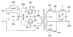
- FIG. 1 is a circuit arrangement of a resonant converter in accordance with a first embodiment of the present invention.
- reference symbol VIN denotes an input voltage supply terminal
- symbol VHI denotes a high voltage output terminal
- VLO denotes a low voltage output terminal.
- a high side power MOS FET Q 1 is connected to the input voltage supply terminal VIN
- a low side power MOS FET Q 2 is grounded.
- Connected between a midpoint of the power MOS FETs Q 1 , Q 2 and the ground voltage are an LC resonance circuit of a capacitor Cr and an inductor Lr, a primary winding 1 of a transformer T 1 , and the primary winding 1 of a current transformer CT, which are connected in series.
- An output of the current transformer CT is connected to an input line x 1 as one input of a PLL (Phase Locked Loop) circuit PLL.
- An output line y of the PLL circuit is connected via a driver DRV to gates of the power MOS FETs Q 1 and Q 2 , and also connected via a delay element DLY to an input line x 2 of the PLL circuit PLL as the other input.
- the power MOS FETs Q 1 and Q 2 including body diodes D 1 and D 2 respectively are driven in mutually opposite phases, and are alternately turned on with a duty of 50%.
- a saturable reactor Ls 1 and a diode D 3 are connected to one secondary winding 21 of the transformer T 1 , while a saturable reactor Ls 2 and a diode D 4 are connected to the other secondary winding 22 .
- Cathodes of the diodes D 3 and D 4 are commonly connected to a cathode of a diode D 7 .
- an anode of the diode D 7 is connected to a center tap of the two secondary windings 21 and 22 of the transformer T 1 and also to the low voltage output terminal VLO of the secondary side.
- a smoothing filter having an inductor L and a capacitor Co is connected between the cathode of the diode D 7 and the low voltage output terminal VLO, and an output of the filter is supplied to the high voltage output terminal VHI.
- the power MOS FETs Q 1 and Q 2 are driven by the driver DRV to convert a direct current of the input voltage supply terminal VIN to an alternating current and to supply the alternating current to the primary winding 1 of the transformer T 1 via the resonance circuit (Cr, Lr).
- An alternating current obtained at the secondary windings 21 and 22 of the transformer T 1 is converted to a direct current and then output controllably by a combination of the saturable reactors Ls 1 and Ls 2 and the diodes D 3 and D 4 . That is, the above circuit arrangement forms a resonant type DC-DC converter.
- the primary side circuit of the transformer T 1 forms a two-transistor resonance circuit
- the secondary side circuit thereof forms an isolated power supply of a DC-DC conversion type having a magamp control circuit provided with a center tap.
- the output frequency fsw for driving of the power MOS FETs Q 1 and Q 2 coincides with the resonant frequency fr.
- the capacitor Cr of the resonance circuit has a capacity Cr and the inductor Lr of the resonance circuit has an inductance Lr
- the resonant frequency fr of the resonance circuit is given by 1 ⁇ 2 ⁇ square root over ( ) ⁇ (Lr ⁇ Cr).
- Soft switching operation is secured usually by finding such values under conditions, fsw ⁇ fr. In this case, it is required to consider the value of the inductance Lr including the value of a leakage inductance of the transformer T 1 . When the value of the leakage inductance is smaller than the value of the inductance Lr to be used, however, the leakage inductance of the transformer T 1 is negligible.
- the point of realization of reliable soft switching operation of the resonant converter is that the relation fsw ⁇ fr is always satisfied between the output frequency fsw and the resonant frequency fr.
- the resonant frequency fr of the resonance circuit remarkably varies with a load variation (including a temperature variation) or variations in characteristics of the components of the resonance circuit.
- the requirement fsw ⁇ fr is required to be met even when the resonant frequency fr varies.
- the principal object is placed on meeting the requirement fsw ⁇ fr, and the frequency tracking control system based on the PLL circuit is employed. When the converter is first turned on, one input line x 1 of the PLL circuit PLL has no signal.
- the oscillation frequency of a variable oscillator within the PLL circuit is output from the output line y of the PLL circuit PLL as the initial value of the output frequency fsw to drive the power MOS FETs Q 1 and Q 2 via the driver DRV.
- the initial oscillation frequency of the variable oscillator is previously set at a frequency (maximum frequency to be explained later) higher than the value fr.
- the PLL circuit modifies the oscillation frequency of the variable oscillator according to the resonant frequency fr in such a manner that the output frequency fsw is equal to the resonant frequency fr.
- the function of the PLL circuit also acts to make equal not only the frequency but also the phase.
- the converter is influenced by the body diodes D 1 and D 2 and output capacities (not shown) of the power MOS FETs Q 1 and Q 2 , thus making it difficult to realize the reliable soft switching operation.
- FIG. 2 shows a waveform of a current for driving a main switching device a waveform of a resonant current in accordance with a first embodiment of the present invention, showing a phase relation therebetween.
- the waveform of the current for driving the power MOS FET Q 1 leads the waveform of the resonant current of the current transformer CT having a zero phase by a phase td.
- a delay element DLY is provided in a feedback loop extended from the output line y of the PLL circuit PLL to the other input line x 2 . This results in that the drive waveform of the main switching device lead the waveform of the resonant current by the phase td and a phase relation necessary for the reliable soft switching operation can be realized.
- FIG. 3 is a specific example of a circuit arrangement of the embodiment of FIG. 1 around the PLL circuit.
- MC14046B manufactured by Motorola Inc. is used as the PLL circuit.
- the minimum oscillation frequency fmin of the variable oscillator is determined by a resistor R 2 and a timing capacitor Cf
- the variable frequency range (fmax to fmin) of the variable oscillator is determined by a resistor R 1 and the timing capacitor Cf.
- a loop filter is composed of a resistor R 3 and a capacitor C 1 .
- the oscillation frequency of the variable oscillator in the PLL circuit is set to start oscillating with its maximum frequency fmax.
- the delay element DLY is composed of two inverters INV 1 and INV 2 , a resistor R 6 , and a capacitor C 4 ; and the delay time td is set by a time constant of the resistor R 6 and the capacitor C 4 and by the logic threshold voltage of the inverter INV 2 .
- Positive and negative resonant currents of the resonance circuit are transmitted to the secondary side of the current transformer CT via the current transformer CT, and the resonant currents are converted to positive and negative voltages via a resistor R 5 . These converted voltages are input to the PLL circuit via a capacitor C 2 for level conversion.
- the variable oscillator within the PLL circuit may oscillate if necessary at an oscillation frequency corresponding to M times the resonant.
- a feedback loop extended from the output of the PLL circuit via a 1/M divider circuit to the delay element is formed.
- the achievement of the reliable soft switching operation leads to reduction of the switching loss of the power MOS FETs Q 1 and Q 2 , thus realizing an increased efficiency.
- the driving frequency fsw of the power MOS FETs Q 1 and Q 2 is made to track the resonant frequency fr determined by the time constant of used components using the PLL circuit. As a result, manufacturing adjustment can be freely made and design and adjusting cost can be reduced.
- a voltage induced at the secondary winding 21 is applied as an energy via the saturable reactor Ls 1 and the diode D 3 to a smoothing filter of the inductor L and the capacitor Co.
- a voltage induced at the secondary winding 22 is applied to the smoothing filter via the saturable reactor Ls 2 and the diode D 4 .
- These saturable reactors Ls 1 and Ls 2 act as magnetic amplifiers well known so far, and can considered to perform the PWM (Pulse Width Modulation) control of the magnetic circuit.
- the reactor when the saturable reactor Ls 1 or Ls 2 is in a reset period and in an unsaturation period, the reactor is considered to be in the off period of the PWM pulse. When the reactor is in a saturation period, the reactor is considered to be in the on period of the PWM pulse and the diode D 3 or D 4 is correspondingly conducted.
- the saturable reactor Ls 1 or Ls 2 is in the unsaturation or reset period, the energy of the smoothing filter and a load (not shown) is circulated through the diode D 7 , like the off period of the PWM pulse. In this manner, an output voltage Vo is eventually obtained between the output terminals VHI and VLO.
- FIG. 4 is a circuit arrangement of a resonant converter in accordance with a second embodiment of the present invention, wherein a magamp control circuit is added to the resonant converter of FIG. 1 .
- FIG. 4 is different from FIG. 1 in that resetting diodes D 5 , D 6 , a magamp control circuit MAG, and a reference voltage Vref are added for control of the saturable reactors Ls 1 and Ls 2 .
- the added circuit acts to compare the output voltage and the reference voltage Vref, and perform negative feedback control over the magamp control circuit MAG in such a manner that the output voltage is equal to the reference voltage Vref.
- the output voltage is higher (lower) than the reference voltage Vref, the output voltage is fed back to the magamp control circuit MAG to decrease (increase) the output, whereby a desired output voltage can be obtained.
- FIG. 5 is a specific circuit diagram of the magamp control circuit used in the embodiment of FIG. 4 .
- the magamp control circuit MAG is composed of an error amplifier EA, a diode D 10 , a bipolar transistor Q 10 , and two resistors 7 and 8 .
- a voltage at the high voltage output terminal VHI or an output voltage of an auxiliary power supply is supplied to a power terminal AUX.
- the bipolar transistor Q 10 operates to cutoff.
- a resets current becomes small, a saturable reactor spreads the saturation period, and a pulse width passing through the diode D 3 or D 4 is controlled to be expanded. If the voltage (output voltage) on the input line a is higher than the voltage (reference voltage) on the input line b, to the contrary, then the bipolar transistor Q 10 acts to be shifted to such a direction as to increase its conduction current. Thus, the reset current becomes large, the saturable reactor expands the reset period (including unsaturation period), and the pulse width passing through the diode D 3 or D 4 is controlled in such a direction as to be narrowed.
- FIG. 6 is a circuit arrangement of a resonant converter in accordance with a third embodiment of the present invention.
- the embodiment of FIG. 6 is different from that of FIG. 4 in that the diodes D 3 and D 4 are replaced by power MOS FETs Q 3 and Q 4 . Since the above replacement enables the power MOS FET to have a low on-resistance, the loss can be reduced and the efficiency can be increased when compared with the use of the diodes.
- Diodes D 31 and D 41 in FIG. 6 are body diodes for the power MOS FETs Q 3 and Q 4 .
- the power MOS FETs Q 3 and Q 4 are driven by gate driving circuit GD 1 and GD 2 respectively.
- FIG. 7 is a specific example of a circuit arrangement of the gate driving apparatus of a power MOS FET used in the embodiment of FIG. 6 .
- a signal extracted from a connection between the saturable reactor Ls 1 or Ls 2 and the transformer is used as an input to drive a transformer T 2 via a level shift circuit of a capacitor C 5 and two resistors R 9 and R 10 and via a buffer circuit BU 1 .
- a voltage induced on the secondary winding of the transformer T 2 is used to drive the gate of the power MOS FET Q 3 or Q 4 .
- FIG. 8 is a circuit arrangement of a resonant converter in accordance with a fourth embodiment of the present invention.
- the diodes D 3 and D 4 in FIG. 4 are replaced by the power MOS FETs Q 3 and Q 4 and the diode D 7 in FIG. 6 is replaced by a power MOS FET Q 7 .
- Gate driving apparatuses GD 3 and GD 4 and an OR gate OR are used to drive the gates of the power MOS FETs Q 3 , Q 4 , and Q 7 used in this example.
- FIG. 9 is a specific example of a circuit arrangement of the gate driving apparatus used in the embodiment of FIG. 8 .
- Differences between the embodiments of FIGS. 9 and 7 are two points. The first point is that the buffer circuit BU 1 in FIG. 7 is replaced by inverters INV 3 and INV 4 and an output at an intermediate connection point between the inverters is supplied to the OR gate OR in FIG. 8 .
- the next different point is that an input line k to the gate driving circuit GD 3 or GD 4 is extracted from the cathode of diode D 5 or D 6 .
- the power MOS FETs Q 3 and Q 4 are turned on in the saturation period of the saturable reactor and are turned off in the off period of the power MOS FETs Q 3 and Q 4 .
- FIG. 10 is a circuit arrangement of a resonant converter in accordance with a fifth embodiment of the present invention.
- the diodes D 3 and D 4 are used as they are in the embodiment of FIG. 4 and the diode D 7 is replaced by a power MOS FET.
- an output voltage is as relatively high as, e.g., a level in a range of 5–12 volts and thus when the forward loss of a rectifier diode causes no serious problems, a circuit component cost or a loss can be reduced.
- the current of the inductor L in the no-load mode can be moved to its continuous mode, the overshoot of the output voltage can be avoided, and the need of a dummy load for suppressing a rise in the output voltage in the no-load state of a discontinuous mode when the free wheel, diode is employed can be eliminated.
- the effect can be similarly obtained even in the foregoing embodiments so long as the free wheel diode is replaced by the power MOS FET.
- FIG. 11 is a circuit arrangement of a resonant converter in accordance with a sixth embodiment of the present invention, wherein a PWM control circuit of a synchronous rectification type is used in a secondary side of a transformer. Accordingly, a saturable reactor is not used in the secondary side of the transformer.
- the power MOS FET Q 3 or Q 4 for passing the voltage from the secondary winding of the transformer therethrough in the foregoing embodiments is replaced by two power MOS FETs Q 31 and Q 32 or Q 41 and Q 42 . Since an arrangement of commonly connecting source electrodes of these two power MOS FETs is employed, a synchronous rectification function can be realized. As a result, these two power MOS FETs are controlled by the PWM control circuit, the gate driving apparatuses GD 1 and GD 2 , and the reference voltage Vref.
- FIG. 12 is a specific circuit arrangement of the PWM control circuit used in the embodiment of FIG. 11 .
- a PWM control circuit PWM includes an error amplifier EA, a voltage-current conversion circuit VI, and one-shot multivibrator OSM 1 or OSM 2 .
- the start timing signal of the one-shot multivibrator is extracted from one of polarity ends of the secondary winding 21 of the transformer T 1 having a black spot applied thereto.
- the extracted signal is input to a signal line d via a level shift circuit having a capacitor C 7 and two resistors R 13 and R 14 .
- An error voltage between the reference voltage and the output voltage is amplified by the error amplifier EA, and the amplified voltage is converted to a current by the voltage-current conversion circuit VI.
- the converted current charges a capacitor CT 1 or CT 2 .
- a PWM on-pulse is generated according to a relationship between the charging voltage and the operational threshold value of the one-shot multivibrator.
- the on-pulse thus generated is output as a signal on a signal line f or g to drive the power MOS FETs Q 31 , Q 32 , Q 41 , and Q 42 .
- the power MOS FET Q 7 is driven by a signal appearing on a signal line e after the signals on the signal lines f and g are passed through the OR gate OR.
- start timing signal of the one-shot multivibrator is extracted from one of the ends of the secondary winding 21 of the transformer T 1 having the black spot applied thereto.
- the start timing signal of the one-shot multivibrator is not limited to the illustrated example.
- the structure of the synchronous rectification circuit is not restricted to the circuit of FIG. 11 alone but a synchronous rectification system such as a current doubler circuit may be employed, exhibiting effects similar to the above cases.
- FIG. 13 is a circuit arrangement of a resonant converter in accordance with a seventh embodiment of the present invention, wherein the resonant converter is used in a multioutput isolated power supply.
- the primary side is a two-transistor resonance circuit using PLL control
- the secondary side is an individual magamp control circuit provided with a center tap. Since the circuit operation of the primary side is independent of the circuit operation of the secondary side, circuit design can be facilitated. Further, control interference between circuits at the secondary side can be made less. And even in the case of the multioutput power supply, in addition to the effects mentioned above, the power supply can advantageously have a smaller number of isolation locations between the primary and secondary sides.
- the saturable reactor is used in the secondary side of the transformer.
- the saturable reactor is not used and a PWM control circuit of an individual synchronous rectification type provided with a center tap may be used, realizing effects similar to the above.
- FIG. 14 is a circuit arrangement of a resonant converter in accordance with an eighth embodiment of the present invention, wherein the transformer is divided.
- the transformer is divided into three sections.
- Primary windings 11 , 12 and 13 of transformers T 11 , T 12 and T 13 have each an identical coil turn number, and due to the presence of leakage inductances (not shown) of the transformers, it is expected to balance the transformers. Since the effect of the transformer division enables use of transformers having a small capacity, a small-size, flat type power supply can be easily constructed.
- FIG. 15 is a specific example of a circuit arrangement of a resonant converter in accordance with a ninth embodiment of the present invention, wherein the driving frequency fsw is set at a value corresponding to 1/N of the resonant frequency fr.
- the power MOS FET is driven with the driving frequency fsw of the power MOS FET set at 1/N of the resonant frequency fr.
- the embodiment of FIG. 15 is different from that of FIG. 1 in that a 1/N divider DIV is inserted in a feedback loop extended from the current transformer CT to the PLL circuit PLL.
- N is required to be one selected from odd numbers of 1, 3, 5, . . . .
- N can take one of odd numbers of 1, 3, 5 . . . .
- the driving frequency fsw of the power MOS FET has a value corresponding to 1/N (odd number) of the resonant frequency fr, a switching loss such as the recovery loss of the body diode of the power MOS FET can be advantageously reduced.
- FIG. 17 is a circuit arrangement of a resonant converter in accordance with a tenth embodiment of the present invention.
- FIG. 17 shows a parallel-connected resonant converter wherein the capacitor Cr is connected in parallel to the load.
- constituent elements having the same reference numerals or symbols as FIG. 1 denote the same elements. Even in such an arrangement, effects similar to the above cases can be obtained.
- FIG. 17 corresponds to the embodiment of FIG. 1 , but can be similarly applied to the arrangements of the aforementioned embodiments.
- an IGBT Insulated Gate Bipolar Transistor
- the power MOS FET Q 1 is of an NMOS type
- the NMOS FET may be replaced by a PMOS FET for its realization.
- the secondary winding of the transformer having the center tap is shown.
- the present invention is not limited to the above example, but may be applied, e.g., to an example of limited use of power corresponding to a half period with use of one winding, obtaining effects similar to the above.
- the resonant converter of the present invention can be applied not only to the isolated power supply for a process input/output device in the computer control system, but also to a multioutput isolated power supply for use in information and communication equipment, electronic equipment, etc.
Landscapes
- Engineering & Computer Science (AREA)
- Power Engineering (AREA)
- Dc-Dc Converters (AREA)
- Rectifiers (AREA)
Abstract
A resonant converter which can realize its easy design, eliminate the need for its adjustment, realize reliable soft switching operation, and increase an efficiency. A driver DRV of a main switching device uses a PLL circuit PLL to apply frequency tracking control in such a manner that a driving frequency fsw is made to track a resonant frequency fr (or 1/N thereof, N being an odd number) and that the phase of the driving frequency fsw leads the current zero phase of the resonant frequency fr always by a desired time. As a result, such an optimum condition can be kept that the main switching device is triggered immediately before the zero-cross point of a resonant current. Thus the resonant converter which can always satisfy the optimum operational conditions, realize soft switching operation, and increase an efficiency can be realized with an easy design and a manufacturing adjustment-free arrangement.
Description
The present invention relates to an improvement in a resonant converter which converts a direct current to an alternating current as an alternating current output by a semiconductor switching device, and supplies the alternating current output to a primary side of a transformer via a resonance circuit to convert an alternating current flowing through a secondary side of the transformer into a direct current.
A DC-DC converter has been widely used as an isolated power supply for the process input/output device of a computer control system or as a multioutput DC power supply for an information and communication equipment, electronic equipment and so on. One of types of such DC-DC converters is a resonant converter, which is disclosed, for example, in JP-A-2002-247854 or in “Multioutput Current-Mode Resonant Converter Using MAGAMP Control”, Switching Power Supply System Symposium 2002, Japan Management Association, (C6-2-1 to C6-2-10) (see C6-2-8 for its entirety and objects) (which will be referred to as Literature 1, hereinafter). That is, the resonant converter basically includes a main switching device (DC-AC converter), a resonance circuit, a transformer, and a rectifier (AC-DC converter). And a smoothly varying current is obtained by the resonance circuit, and a switching loss is reduced by the soft switching of the switching device in the vicinity of a zero voltage and a zero current thereof, thus realizing a high efficiency and low noise.
As disclosed in Literature 1, the above resonant converter is difficult in the design and computation of an operating frequency because a load resistance varies according to an output condition. A resonant frequency also varies according to not only the load variation but also variations in the characteristics between the components of the resonance circuit. In order to realize the soft switching operation of the resonant converter, a driving frequency fsw of the main switching device is required to be kept at a resonant frequency fr of the resonance circuit or higher. For this reason, circuit design becomes troublesome due to the aforementioned load variation or variations in the resonance circuit components.
It is therefore an object of the present invention to provide a resonant converter which can realize easy design and reliable soft switching operation even in the presence of variations in characteristics between the components of a resonance circuit.
Another object of the present invention is to realize a control method of a resonant converter which can attain continuous soft switching operation even in the presence of a load variation or variations in characteristics between the components of a resonance circuit.
In an aspect of the present invention, the output frequency fsw of a driving section for driving a main switching device is made to track the resonant frequency fr of the resonance circuit or a frequency corresponding to 1/(odd number) thereof.
In an embodiment of the aspect of the present invention, the output frequency fsw of the driving section is made to track the resonant frequency fr under control of frequency tracking using a PLL (Phase Locked Loop) circuit.
In another aspect of the present invention, the output frequency fsw of the driving section for driving the main switching device is made to track the resonant frequency fr of the resonance circuit or a frequency corresponding to 1/(odd number) thereof, and the driving section is designed to generate an output signal which leads the zero-cross point of a resonant current of the resonance circuit in phase.
In accordance with the present invention, there is provided a resonant converter which can realize easy design and reliable soft switching operation even in the presence of a load variation or variations in characteristics between the components of a resonance circuit.
In the other aspect of the present invention, there is provided a control method for a resonant converter which can realize continuous soft switching operation even in the presence of a load variation or variations in characteristics between the components of a resonance circuit.
Other objects, features and advantages of the invention will become apparent from the following description of the embodiments of the invention taken in conjunction with the accompanying drawings.
A saturable reactor Ls1 and a diode D3 are connected to one secondary winding 21 of the transformer T1, while a saturable reactor Ls2 and a diode D4 are connected to the other secondary winding 22. Cathodes of the diodes D3 and D4 are commonly connected to a cathode of a diode D7. And an anode of the diode D7 is connected to a center tap of the two secondary windings 21 and 22 of the transformer T1 and also to the low voltage output terminal VLO of the secondary side. A smoothing filter having an inductor L and a capacitor Co is connected between the cathode of the diode D7 and the low voltage output terminal VLO, and an output of the filter is supplied to the high voltage output terminal VHI.
In this circuit arrangement, the power MOS FETs Q1 and Q2 are driven by the driver DRV to convert a direct current of the input voltage supply terminal VIN to an alternating current and to supply the alternating current to the primary winding 1 of the transformer T1 via the resonance circuit (Cr, Lr). An alternating current obtained at the secondary windings 21 and 22 of the transformer T1 is converted to a direct current and then output controllably by a combination of the saturable reactors Ls1 and Ls2 and the diodes D3 and D4. That is, the above circuit arrangement forms a resonant type DC-DC converter. In other words, the primary side circuit of the transformer T1 forms a two-transistor resonance circuit, and the secondary side circuit thereof forms an isolated power supply of a DC-DC conversion type having a magamp control circuit provided with a center tap.
Explanation will next be made as to the circuit operation of FIG. 1 . In the usual operation of the resonant converter, when the power MOS FET Q1 is first turned on (the power MOS FET Q2 in its off state), a direct voltage is applied from the input voltage supply terminal VIN to the resonance circuit of the capacitor Cr and the inductor Lr, so that a positive resonant current starts to flow through the resonance circuit. A period, during which the positive resonant current flows, corresponds to ½ of the reciprocal of the resonant frequency fr of the resonance circuit (half period). In the next half period, when the power MOS FET Q2 is turned on (power MOS FET Q1 is turned off), a negative resonant current starts to flow through the resonance circuit. For this reason, in the resonant type converter, it is necessary to make the output frequency fsw for driving of the power MOS FETs Q1 and Q2 coincide with the resonant frequency fr. Assuming in this example that the capacitor Cr of the resonance circuit has a capacity Cr and the inductor Lr of the resonance circuit has an inductance Lr, then the resonant frequency fr of the resonance circuit is given by ½π√{square root over ( )} (Lr·Cr). Thus, when the output frequency fsw for driving the power MOS FETs Q1 and Q2 is determined, the values of the inductance Lr and the capacity Cr are determined by substituting the determined output frequency for fr. Soft switching operation is secured usually by finding such values under conditions, fsw≧fr. In this case, it is required to consider the value of the inductance Lr including the value of a leakage inductance of the transformer T1. When the value of the leakage inductance is smaller than the value of the inductance Lr to be used, however, the leakage inductance of the transformer T1 is negligible.
The point of realization of reliable soft switching operation of the resonant converter is that the relation fsw≧fr is always satisfied between the output frequency fsw and the resonant frequency fr. As mentioned above, the resonant frequency fr of the resonance circuit remarkably varies with a load variation (including a temperature variation) or variations in characteristics of the components of the resonance circuit. Thus the requirement fsw≧fr is required to be met even when the resonant frequency fr varies. To this end, the principal object is placed on meeting the requirement fsw≧fr, and the frequency tracking control system based on the PLL circuit is employed. When the converter is first turned on, one input line x1 of the PLL circuit PLL has no signal. As a result, the oscillation frequency of a variable oscillator within the PLL circuit is output from the output line y of the PLL circuit PLL as the initial value of the output frequency fsw to drive the power MOS FETs Q1 and Q2 via the driver DRV. In this case, since it is necessary to meet the requirement fsw≧fr even in the no-signal duration, the initial oscillation frequency of the variable oscillator is previously set at a frequency (maximum frequency to be explained later) higher than the value fr. When the converter is operated in this way, a resonant current starts to flow through the resonance circuit, and the resonant current is detected by the current transformer CT. When zero-phase information about the detected resonant current is applied to one input line x1 of the PLL circuit PLL, the PLL circuit modifies the oscillation frequency of the variable oscillator according to the resonant frequency fr in such a manner that the output frequency fsw is equal to the resonant frequency fr. The function of the PLL circuit also acts to make equal not only the frequency but also the phase. When these two frequencies become equal to each other and the phases are also made equal, however, the converter is influenced by the body diodes D1 and D2 and output capacities (not shown) of the power MOS FETs Q1 and Q2, thus making it difficult to realize the reliable soft switching operation. To avoid this and realize the reliable soft switching operation, it is necessary to set the phase relation between two frequencies as shown by operational waveforms in FIG. 2 .
Although the resonant frequency fr is designed to be the same as the output frequency fsw of the variable oscillator within the PLL circuit in the present embodiment, the variable oscillator within the PLL circuit may oscillate if necessary at an oscillation frequency corresponding to M times the resonant. In this case, a feedback loop extended from the output of the PLL circuit via a 1/M divider circuit to the delay element is formed. Thus, when a drive signal to the driver DRV is extracted from the midpoint of the divider circuit and the delay element, PLL operation can be achieved in a similar manner to the above.
As has been mentioned above, the achievement of the reliable soft switching operation leads to reduction of the switching loss of the power MOS FETs Q1 and Q2, thus realizing an increased efficiency. Further, with regard to variations in characteristics between the components of the resonance circuit, the driving frequency fsw of the power MOS FETs Q1 and Q2 is made to track the resonant frequency fr determined by the time constant of used components using the PLL circuit. As a result, manufacturing adjustment can be freely made and design and adjusting cost can be reduced.
Explanation will then be made as to the operation of obtaining a direct output voltage at the secondary side circuit of the transformer T1. Referring back to FIG. 1 , a voltage induced at the secondary winding 21 is applied as an energy via the saturable reactor Ls1 and the diode D3 to a smoothing filter of the inductor L and the capacitor Co. Similarly, a voltage induced at the secondary winding 22 is applied to the smoothing filter via the saturable reactor Ls2 and the diode D4. These saturable reactors Ls1 and Ls2 act as magnetic amplifiers well known so far, and can considered to perform the PWM (Pulse Width Modulation) control of the magnetic circuit. More specifically, when the saturable reactor Ls1 or Ls2 is in a reset period and in an unsaturation period, the reactor is considered to be in the off period of the PWM pulse. When the reactor is in a saturation period, the reactor is considered to be in the on period of the PWM pulse and the diode D3 or D4 is correspondingly conducted. When the saturable reactor Ls1 or Ls2 is in the unsaturation or reset period, the energy of the smoothing filter and a load (not shown) is circulated through the diode D7, like the off period of the PWM pulse. In this manner, an output voltage Vo is eventually obtained between the output terminals VHI and VLO.
In the present embodiment, in addition to the fact that a saturable reactor having a large capacity and components associated therewith can be omitted, an increased efficiency can be realized like the above cases.
The structure of the synchronous rectification circuit is not restricted to the circuit of FIG. 11 alone but a synchronous rectification system such as a current doubler circuit may be employed, exhibiting effects similar to the above cases.
According to the present embodiment, since the driving frequency fsw of the power MOS FET has a value corresponding to 1/N (odd number) of the resonant frequency fr, a switching loss such as the recovery loss of the body diode of the power MOS FET can be advantageously reduced.
In the present invention, an IGBT (Insulated Gate Bipolar Transistor) in place of the power MOS FET can be used as the main switching device for its realization. Although explanation has been on the assumption that the power MOS FET Q1 is of an NMOS type, the NMOS FET may be replaced by a PMOS FET for its realization.
In the foregoing explanation, the secondary winding of the transformer having the center tap is shown. However, the present invention is not limited to the above example, but may be applied, e.g., to an example of limited use of power corresponding to a half period with use of one winding, obtaining effects similar to the above.
The resonant converter of the present invention can be applied not only to the isolated power supply for a process input/output device in the computer control system, but also to a multioutput isolated power supply for use in information and communication equipment, electronic equipment, etc.
It should be further understood by those skilled in the art that although the foregoing description has been made on embodiments of the invention, the invention is not limited thereto and various changes and modifications may be made without departing from the spirit of the invention and the scope of the appended claims.
Claims (20)
1. A resonant converter for converting a direct current to an alternating current as an alternating current output at a semiconductor switching device driven by a driving section, supplying the alternating current output to a primary side of a transformer via resonance circuit, and converting an alternating current flowing through a secondary side of the transformer to a direct current, said converter comprising:
means for making an output frequency of said driving section for driving said semiconductor switching device track a resonant frequency of said resonance circuit or a frequency corresponding to 1/(odd number) thereof.
2. A resonant converter according to claim 1 , wherein means for making the output frequency of said driving section track a resonant frequency of said resonance circuit or a frequency corresponding to 1/(odd number) thereof is provided with a PLL (Phase Locked Loop) circuit.
3. A resonant converter according to claim 1 , wherein a saturable reactor is provided in the secondary side of said transformer.
4. A resonant converter according to claim 1 , wherein a switching device to be driven by a voltage of the secondary side of said transformer is provided in the secondary side of said transformer.
5. A resonant converter according to claim 1 , wherein switching means for switchingly converting a voltage of the secondary side of said transformer to a direct current, a smoothing filter connected to an output side of said switching means and including an inductor and a capacitor, a switching device connected with such a direction as to circulate a current flowing through said smoothing filter and/or a load, and means for driving said switching device during an off period of said switching means are provided in the secondary side of said transformer.
6. A resonant converter according to claim 1 , comprising a synchronous rectification circuit provided with a center tap connected to the secondary side of said transformer and including a switching device, and means for performing PWM control over said switching device.
7. A resonant converter according to claim 1 , comprising a plurality of secondary windings of said transformer and means for converting alternating voltages of the plurality of secondary windings to direct voltages respectively.
8. A resonant converter according to claim 1 , wherein said converter comprises a plurality of transformers, and said common semiconductor switching device and said resonance circuit are connected to primary sides of said plurality of transformers to convert alternating currents flowing through secondary sides of said plurality of transformers to a plurality of direct currents and to output a plurality of direct voltages respectively.
9. A resonant converter according to claim 1 , wherein said means for making the output frequency of said driving section for driving said semiconductor switching device track the resonant frequency of said resonance circuit is arranged to track a frequency corresponding to ⅓ of said resonant frequency.
10. A resonant converter for converting a direct current to an alternating current as an alternating current output at a semiconductor switching device driven by a driving section, supplying the alternating current output to a primary side of a transformer via resonance circuit, and converting an alternating current flowing through a secondary side of the transformer to a direct current, said converter comprising:
means for making an output frequency of said driving section for driving said semiconductor switching device track a resonant frequency of said resonance circuit or a frequency corresponding to 1/(odd number) thereof, and
means for generating the output signal of said driving section with a phase leading a zero-cross point of the resonance current of said resonance circuit.
11. A resonant converter according to claim 10 , comprising a PLL (Phase Locked Loop) circuit for outputting a frequency made to track the resonant frequency of said resonance circuit or a frequency corresponding to 1/(odd number) thereof, and a delay element provided in a feedback loop of said PLL circuit; and wherein said switching device is driven on the basis of an output signal of said PLL circuit.
12. A resonant converter according to claim 10 , wherein a saturable reactor is provided in the secondary side of said transformer.
13. A resonant converter according to claim 10 , wherein a switching device driven by a voltage of the secondary side of said transformer is provided in the secondary side of said transformer.
14. A resonant converter according to claim 10 , wherein switching means for switchingly converting a voltage of the secondary side of said transformer to a direct voltage, a smoothing filter connected to an output side of said switching means and including an inductor and a capacitor, a switching device connected in such a direction as to circulate a current flowing through said smoothing filter and/or a load, and means for driving said switching device during an off period of said switching device are provided in the secondary side of said transformer.
15. A resonant converter according to claim 10 , comprising a synchronous rectification circuit provided with a center tap connected to the secondary side of said transformer and including a switching device, and control means for performing PWM control over said switching device.
16. A resonant converter according to claim 10 , comprising a plurality of secondary windings of said transformer and means for converting alternating voltages of said plurality of secondary windings to direct voltages respectively.
17. A resonant converter according to claim 10 , wherein said converter comprises a plurality of transformers, and said semiconductor switching device and said resonance circuit are commonly connected to primary sides of said plurality of transformers to convert alternating currents flowing through secondary sides of said plurality of transformers to a plurality of direct currents and to output a plurality of direct voltages respectively.
18. A resonant converter according to claim 10 , wherein said means for making the operating frequency of said driving section for driving said semiconductor switching device track the resonant frequency of said resonance circuit is arranged to track a frequency corresponding to ⅓ of said resonant frequency.
19. A method of controlling a resonant converter for converting a direct current to an alternating current as an alternating current output at a semiconductor switching device driven by a driving section, supplying the alternating current output to a primary side of a transformer via resonance circuit, and converting an alternating current flowing through a secondary side of the transformer to a direct current, said method comprising the step of:
making an output frequency of said driving section for driving said semiconductor switching device track a resonant frequency of said resonance circuit or a frequency corresponding to 1/(odd number) thereof.
20. A method according to claim 19 , wherein the output signal of said driving section is generated with a phase leading a zero-cross point of the resonance current of said resonance circuit.
Applications Claiming Priority (2)
| Application Number | Priority Date | Filing Date | Title |
|---|---|---|---|
| JP2003-380846 | 2003-11-11 | ||
| JP2003380846A JP2005151608A (en) | 2003-11-11 | 2003-11-11 | Resonance converter and its control method |
Publications (2)
| Publication Number | Publication Date |
|---|---|
| US20050099827A1 US20050099827A1 (en) | 2005-05-12 |
| US7088594B2 true US7088594B2 (en) | 2006-08-08 |
Family
ID=34544613
Family Applications (1)
| Application Number | Title | Priority Date | Filing Date |
|---|---|---|---|
| US10/984,846 Expired - Fee Related US7088594B2 (en) | 2003-11-11 | 2004-11-10 | Resonant converter and control method thereof |
Country Status (2)
| Country | Link |
|---|---|
| US (1) | US7088594B2 (en) |
| JP (1) | JP2005151608A (en) |
Cited By (9)
| Publication number | Priority date | Publication date | Assignee | Title |
|---|---|---|---|---|
| US20070070655A1 (en) * | 2003-12-11 | 2007-03-29 | Honda Motor Co., Ltd. | Dc-dc converter |
| US20080298094A1 (en) * | 2007-06-01 | 2008-12-04 | Cuadra Jason E | Method and apparatus to control two regulated outputs of a flyback power supply |
| US20100149843A1 (en) * | 2008-05-02 | 2010-06-17 | Hendrik Walde | Preemptive protection for a power convertor |
| CN101888187A (en) * | 2009-05-11 | 2010-11-17 | 英特赛尔美国股份有限公司 | The control model of ZVS converter under resonant operational frequency |
| US20120039378A1 (en) * | 2010-08-16 | 2012-02-16 | Kazuaki Nakayama | Converter and converter control method |
| TWI407674B (en) * | 2009-10-21 | 2013-09-01 | ||
| CN104600968A (en) * | 2015-02-09 | 2015-05-06 | 广西师范大学 | Digital current tracking and synchronizing method and device for high-frequency resonant soft-switching circuit |
| EP3796344A1 (en) * | 2019-09-20 | 2021-03-24 | ABB Power Grids Switzerland AG | Winding configuration as part of an integrated structure for a medium frequency transformer |
| US11088655B2 (en) * | 2018-01-31 | 2021-08-10 | Sungrow Power Supply Co., Ltd. | Photovoltaic solid-state transformer, photovoltaic inverter system and bidirectional high-voltage converter |
Families Citing this family (42)
| Publication number | Priority date | Publication date | Assignee | Title |
|---|---|---|---|---|
| DE10347193A1 (en) * | 2003-10-10 | 2005-05-12 | Thomson Brandt Gmbh | Switching Power Supply |
| US7006364B2 (en) * | 2004-03-15 | 2006-02-28 | Delta Electronics, Inc. | Driving circuit for DC/DC converter |
| US7592775B2 (en) * | 2006-05-31 | 2009-09-22 | Aeroflex Plainview, Inc. | Battery balancing including resonant frequency compensation |
| US9705325B2 (en) * | 2006-06-01 | 2017-07-11 | Linear Technology Corporation | Controlling switching circuits to balance power or current drawn from multiple power supply inputs |
| JP5607926B2 (en) * | 2006-06-20 | 2014-10-15 | コーニンクレッカ フィリップス エヌ ヴェ | Method for operating resonant power supply and resonant power supply |
| WO2008032362A1 (en) * | 2006-09-12 | 2008-03-20 | Mitsubishi Electric Corporation | Dc/dc converter device |
| WO2008032425A1 (en) * | 2006-09-15 | 2008-03-20 | Mitsubishi Electric Corporation | Dc/dc power converting apparatus |
| EP2063519B1 (en) | 2006-09-15 | 2018-10-31 | Mitsubishi Electric Corporation | Dc/dc power converter |
| JP4468933B2 (en) * | 2006-09-28 | 2010-05-26 | 三菱電機株式会社 | Power converter |
| US8023296B2 (en) * | 2007-09-06 | 2011-09-20 | General Electric Company | High voltage, high speed, high pulse repetition rate pulse generator |
| US8279648B2 (en) * | 2008-03-20 | 2012-10-02 | Pratt & Whitney Canada Corp. | Power inverter and method |
| TW200950299A (en) * | 2008-05-30 | 2009-12-01 | Gio Optoelectronics Corp | Single-stage AC to DC conversion device |
| KR100975925B1 (en) * | 2008-07-25 | 2010-08-13 | 삼성전기주식회사 | Adapter power supply |
| PL2323577T3 (en) * | 2008-09-08 | 2016-10-31 | Soft generator | |
| TWI393337B (en) * | 2009-07-31 | 2013-04-11 | Delta Electronics Inc | Two stage switching power conversion circuit |
| FR2953076B1 (en) * | 2009-11-26 | 2012-01-20 | Centre Nat Etd Spatiales | CONTINUOUS-CONTINUOUS CONVERTER OF ELECTRIC ENERGY FROM A CONTINUOUS ELECTRIC ENERGY SOURCE |
| CN102340251B (en) * | 2010-07-20 | 2014-06-04 | 台达电子工业股份有限公司 | Alternating-current to direct-current converter and control circuit thereof |
| US9124190B2 (en) * | 2010-09-02 | 2015-09-01 | Telefonaktiebolaget L M Ericsson (Publ) | Isolated switched mode power supply |
| JP5498347B2 (en) * | 2010-10-20 | 2014-05-21 | 株式会社メガチップス | PLC / power hybrid device and device with communication function |
| CN103250337B (en) * | 2010-12-02 | 2015-12-09 | 株式会社村田制作所 | Switching power circuit |
| EP2479879A1 (en) * | 2011-01-19 | 2012-07-25 | Power Research Electronics B.v. | Resonat power converter |
| WO2013190432A2 (en) * | 2012-06-19 | 2013-12-27 | Koninklijke Philips N.V. | Control modes for resonant dc-to-dc converter |
| US9190898B2 (en) * | 2012-07-06 | 2015-11-17 | Power Systems Technologies, Ltd | Controller for a power converter and method of operating the same |
| US9444346B2 (en) * | 2013-10-17 | 2016-09-13 | Futurewei Technologies, Inc. | Apparatus and efficiency point tracking method for high efficiency resonant converters |
| JP6091643B2 (en) * | 2013-10-31 | 2017-03-08 | 三菱電機エンジニアリング株式会社 | Resonance type high frequency power supply device and switching circuit for resonance type high frequency power supply device |
| CN104795984B (en) * | 2014-01-21 | 2017-09-26 | 华为技术有限公司 | Power supply changeover device |
| US9331584B2 (en) * | 2014-06-30 | 2016-05-03 | Sanken Electric Co., Ltd. | Switching power-supply device |
| TWI533579B (en) * | 2014-10-01 | 2016-05-11 | 財團法人工業技術研究院 | Output power adjusting method for inverter |
| JP6503268B2 (en) * | 2015-09-07 | 2019-04-17 | 東洋電機製造株式会社 | Control method and control device for series resonance type power supply device |
| JP6866729B2 (en) | 2017-03-31 | 2021-04-28 | スミダコーポレーション株式会社 | Phase adjustment circuit, inverter circuit and power supply device |
| EP3447890B1 (en) | 2017-08-21 | 2021-01-13 | Flex, Ltd. | Reconfigurable line modulated resonant converter |
| US10917001B2 (en) | 2017-08-21 | 2021-02-09 | Flex Ltd. | Adaptive resonant frequency converter |
| JP7005286B2 (en) * | 2017-11-01 | 2022-01-21 | 株式会社東芝 | Power supply for electric cars |
| JP6787505B2 (en) * | 2017-12-06 | 2020-11-18 | 富士電機株式会社 | Control method and control circuit of switching power supply |
| JP6801816B2 (en) | 2018-02-15 | 2020-12-16 | 富士電機株式会社 | Switching power supply |
| JP6863337B2 (en) * | 2018-05-30 | 2021-04-21 | 横河電機株式会社 | Pulse signal output circuit |
| EP3815229A1 (en) * | 2018-07-01 | 2021-05-05 | Friedrich-Alexander-Universität Erlangen-Nürnberg | Electromagnetic interference suppression components |
| CN108880265B (en) * | 2018-07-06 | 2019-08-20 | 华南理工大学 | A kind of LLC resonant converter automatic resonance frequency tracker method |
| US11411510B2 (en) * | 2020-01-24 | 2022-08-09 | Lear Corporation | DC/AC inverter resonance topology |
| CN113131750B (en) * | 2021-04-13 | 2022-06-28 | 上海交通大学 | Secondary-side clamping type phase-shifted full-bridge converter |
| US20220399821A1 (en) * | 2021-06-15 | 2022-12-15 | Texas Instruments Incorporated | Llc converter and control |
| US11855530B1 (en) * | 2022-08-05 | 2023-12-26 | Monolithic Power Systems, Inc. | Resonant converter with multiple resonant tank circuits |
Citations (3)
| Publication number | Priority date | Publication date | Assignee | Title |
|---|---|---|---|---|
| US3743919A (en) * | 1972-06-14 | 1973-07-03 | Raytheon Co | Regulated cycloconverter |
| JP2002247854A (en) | 2001-02-20 | 2002-08-30 | Fuji Electric Co Ltd | Direct current/direct current converter |
| US6949915B2 (en) * | 2003-07-24 | 2005-09-27 | Harman International Industries, Incorporated | Opposed current converter power factor correcting power supply |
-
2003
- 2003-11-11 JP JP2003380846A patent/JP2005151608A/en not_active Withdrawn
-
2004
- 2004-11-10 US US10/984,846 patent/US7088594B2/en not_active Expired - Fee Related
Patent Citations (3)
| Publication number | Priority date | Publication date | Assignee | Title |
|---|---|---|---|---|
| US3743919A (en) * | 1972-06-14 | 1973-07-03 | Raytheon Co | Regulated cycloconverter |
| JP2002247854A (en) | 2001-02-20 | 2002-08-30 | Fuji Electric Co Ltd | Direct current/direct current converter |
| US6949915B2 (en) * | 2003-07-24 | 2005-09-27 | Harman International Industries, Incorporated | Opposed current converter power factor correcting power supply |
Non-Patent Citations (1)
| Title |
|---|
| Multioutput Current-Mode Resonant Converter Using MAGAMP Control, Switching Power Supply System Symposium, 2002, Japan Management Association, pp. C6-2-1 to C6-2-10). |
Cited By (15)
| Publication number | Priority date | Publication date | Assignee | Title |
|---|---|---|---|---|
| US20070070655A1 (en) * | 2003-12-11 | 2007-03-29 | Honda Motor Co., Ltd. | Dc-dc converter |
| US20080298094A1 (en) * | 2007-06-01 | 2008-12-04 | Cuadra Jason E | Method and apparatus to control two regulated outputs of a flyback power supply |
| US7675761B2 (en) * | 2007-06-01 | 2010-03-09 | Power Integrations, Inc. | Method and apparatus to control two regulated outputs of a flyback power supply |
| US20100149843A1 (en) * | 2008-05-02 | 2010-06-17 | Hendrik Walde | Preemptive protection for a power convertor |
| US8391025B2 (en) * | 2008-05-02 | 2013-03-05 | Advanced Energy Industries, Inc. | Preemptive protection for a power convertor |
| US9042121B2 (en) | 2008-12-29 | 2015-05-26 | Advanced Energy Industries, Inc. | Power converter with preemptive protection |
| CN101888187A (en) * | 2009-05-11 | 2010-11-17 | 英特赛尔美国股份有限公司 | The control model of ZVS converter under resonant operational frequency |
| TWI407674B (en) * | 2009-10-21 | 2013-09-01 | ||
| US8379412B2 (en) * | 2010-08-16 | 2013-02-19 | Empire Technology Development Llc | Converter and converter control method |
| US20120039378A1 (en) * | 2010-08-16 | 2012-02-16 | Kazuaki Nakayama | Converter and converter control method |
| CN104600968A (en) * | 2015-02-09 | 2015-05-06 | 广西师范大学 | Digital current tracking and synchronizing method and device for high-frequency resonant soft-switching circuit |
| CN104600968B (en) * | 2015-02-09 | 2017-05-10 | 广西师范大学 | Digital current tracking and synchronizing method and device for high-frequency resonant soft-switching circuit |
| US11088655B2 (en) * | 2018-01-31 | 2021-08-10 | Sungrow Power Supply Co., Ltd. | Photovoltaic solid-state transformer, photovoltaic inverter system and bidirectional high-voltage converter |
| EP3796344A1 (en) * | 2019-09-20 | 2021-03-24 | ABB Power Grids Switzerland AG | Winding configuration as part of an integrated structure for a medium frequency transformer |
| WO2021052713A1 (en) * | 2019-09-20 | 2021-03-25 | Abb Power Grids Switzerland Ag | Winding configuration as part of an integrated structure for a medium frequency transformer |
Also Published As
| Publication number | Publication date |
|---|---|
| JP2005151608A (en) | 2005-06-09 |
| US20050099827A1 (en) | 2005-05-12 |
Similar Documents
| Publication | Publication Date | Title |
|---|---|---|
| US7088594B2 (en) | Resonant converter and control method thereof | |
| US9318967B2 (en) | DC to DC converter and DC to DC conversion system | |
| US8441812B2 (en) | Series resonant converter having a circuit configuration that prevents leading current | |
| US7656686B2 (en) | Switching power supply circuit | |
| US6781853B2 (en) | Method and apparatus for reduction of energy loss due to body diode conduction in synchronous rectifiers | |
| US20160013724A1 (en) | Multiphase DC/DC Converters And Control Circuits For Controlling Converters Using Fixed And/Or Variable Frequencies | |
| US8619438B2 (en) | Resonant converter | |
| US7706153B2 (en) | DC-DC Converter | |
| EP3678288B1 (en) | Hybrid switched-capacitor converter | |
| US20080037290A1 (en) | Ac-dc converter and method for driving for ac-dc converter | |
| US20170222545A1 (en) | Power factor improving converter, and power supply device including power factor improving converter | |
| JP7439671B2 (en) | Switching power supplies and power supply systems | |
| US10784859B2 (en) | Transformer based gate drive circuit | |
| US5977753A (en) | Buck regulator with plural outputs | |
| JP2012050264A (en) | Load driving device | |
| JP6241334B2 (en) | Current resonance type DCDC converter | |
| US6744647B2 (en) | Parallel connected converters apparatus and methods using switching cycle with energy holding state | |
| JP4355712B2 (en) | Switching power supply | |
| JP3574849B2 (en) | DC-DC converter device | |
| US7019986B2 (en) | Power conversion apparatus and dead time generator | |
| US11973440B2 (en) | Isolated DC/DC converter with secondary-side full bridge diode rectifier and asymmetrical auxiliary capacitor | |
| JP4434010B2 (en) | DC converter | |
| KR100988324B1 (en) | High step-up dc-dc converter with high efficiency | |
| JP3699011B2 (en) | Switching regulator | |
| JP4107826B2 (en) | Power circuit |
Legal Events
| Date | Code | Title | Description |
|---|---|---|---|
| AS | Assignment |
Owner name: HITACHI LTD., JAPAN Free format text: ASSIGNMENT OF ASSIGNORS INTEREST;ASSIGNORS:SASE, TAKASHI;KANOUDA, AKIHIKO;NAGAYAMA, TETSUYA;AND OTHERS;REEL/FRAME:015987/0008;SIGNING DATES FROM 20041027 TO 20041028 |
|
| REMI | Maintenance fee reminder mailed | ||
| LAPS | Lapse for failure to pay maintenance fees | ||
| STCH | Information on status: patent discontinuation |
Free format text: PATENT EXPIRED DUE TO NONPAYMENT OF MAINTENANCE FEES UNDER 37 CFR 1.362 |
|
| FP | Lapsed due to failure to pay maintenance fee |
Effective date: 20100808 |