US6992902B2 - Full bridge converter with ZVS via AC feedback - Google Patents
Full bridge converter with ZVS via AC feedback Download PDFInfo
- Publication number
- US6992902B2 US6992902B2 US10/644,906 US64490603A US6992902B2 US 6992902 B2 US6992902 B2 US 6992902B2 US 64490603 A US64490603 A US 64490603A US 6992902 B2 US6992902 B2 US 6992902B2
- Authority
- US
- United States
- Prior art keywords
- power
- transformer
- primary
- power converter
- winding
- Prior art date
- Legal status (The legal status is an assumption and is not a legal conclusion. Google has not performed a legal analysis and makes no representation as to the accuracy of the status listed.)
- Expired - Lifetime, expires
Links
Images


Classifications
-
- H—ELECTRICITY
- H02—GENERATION; CONVERSION OR DISTRIBUTION OF ELECTRIC POWER
- H02M—APPARATUS FOR CONVERSION BETWEEN AC AND AC, BETWEEN AC AND DC, OR BETWEEN DC AND DC, AND FOR USE WITH MAINS OR SIMILAR POWER SUPPLY SYSTEMS; CONVERSION OF DC OR AC INPUT POWER INTO SURGE OUTPUT POWER; CONTROL OR REGULATION THEREOF
- H02M7/00—Conversion of ac power input into dc power output; Conversion of dc power input into ac power output
- H02M7/42—Conversion of dc power input into ac power output without possibility of reversal
- H02M7/44—Conversion of dc power input into ac power output without possibility of reversal by static converters
- H02M7/48—Conversion of dc power input into ac power output without possibility of reversal by static converters using discharge tubes with control electrode or semiconductor devices with control electrode
- H02M7/53—Conversion of dc power input into ac power output without possibility of reversal by static converters using discharge tubes with control electrode or semiconductor devices with control electrode using devices of a triode or transistor type requiring continuous application of a control signal
- H02M7/537—Conversion of dc power input into ac power output without possibility of reversal by static converters using discharge tubes with control electrode or semiconductor devices with control electrode using devices of a triode or transistor type requiring continuous application of a control signal using semiconductor devices only, e.g. single switched pulse inverters
- H02M7/5387—Conversion of dc power input into ac power output without possibility of reversal by static converters using discharge tubes with control electrode or semiconductor devices with control electrode using devices of a triode or transistor type requiring continuous application of a control signal using semiconductor devices only, e.g. single switched pulse inverters in a bridge configuration
-
- H—ELECTRICITY
- H02—GENERATION; CONVERSION OR DISTRIBUTION OF ELECTRIC POWER
- H02M—APPARATUS FOR CONVERSION BETWEEN AC AND AC, BETWEEN AC AND DC, OR BETWEEN DC AND DC, AND FOR USE WITH MAINS OR SIMILAR POWER SUPPLY SYSTEMS; CONVERSION OF DC OR AC INPUT POWER INTO SURGE OUTPUT POWER; CONTROL OR REGULATION THEREOF
- H02M3/00—Conversion of dc power input into dc power output
- H02M3/22—Conversion of dc power input into dc power output with intermediate conversion into ac
- H02M3/24—Conversion of dc power input into dc power output with intermediate conversion into ac by static converters
- H02M3/28—Conversion of dc power input into dc power output with intermediate conversion into ac by static converters using discharge tubes with control electrode or semiconductor devices with control electrode to produce the intermediate ac
- H02M3/325—Conversion of dc power input into dc power output with intermediate conversion into ac by static converters using discharge tubes with control electrode or semiconductor devices with control electrode to produce the intermediate ac using devices of a triode or a transistor type requiring continuous application of a control signal
- H02M3/335—Conversion of dc power input into dc power output with intermediate conversion into ac by static converters using discharge tubes with control electrode or semiconductor devices with control electrode to produce the intermediate ac using devices of a triode or a transistor type requiring continuous application of a control signal using semiconductor devices only
- H02M3/33569—Conversion of dc power input into dc power output with intermediate conversion into ac by static converters using discharge tubes with control electrode or semiconductor devices with control electrode to produce the intermediate ac using devices of a triode or a transistor type requiring continuous application of a control signal using semiconductor devices only having several active switching elements
- H02M3/33573—Full-bridge at primary side of an isolation transformer
-
- H—ELECTRICITY
- H02—GENERATION; CONVERSION OR DISTRIBUTION OF ELECTRIC POWER
- H02M—APPARATUS FOR CONVERSION BETWEEN AC AND AC, BETWEEN AC AND DC, OR BETWEEN DC AND DC, AND FOR USE WITH MAINS OR SIMILAR POWER SUPPLY SYSTEMS; CONVERSION OF DC OR AC INPUT POWER INTO SURGE OUTPUT POWER; CONTROL OR REGULATION THEREOF
- H02M3/00—Conversion of dc power input into dc power output
- H02M3/01—Resonant DC/DC converters
Definitions
- This invention generally relates to the field of power converters, and more particularly, to full bridge converters that operate with zero-voltage switching (ZVS).
- ZVS zero-voltage switching
- Full-bridge switching power converters are a common DC/DC conversion topology used for supplying high power to a wide variety of electronic components, including telecommunication equipments, computers, servers, etc.
- a DC/DC switching converter contains an input port typically coupled to a DC power source, such as a battery, to provide DC power to a load connected to an output port.
- full-bridge converters utilize two bridge legs with four switching elements in the primary side of a transformer that isolates the input port from the output port.
- a pulse width modulator is used to regulate the output voltage under various load conditions.
- Power density relates to the amount of delivered power relative to the volume occupied by the power converter, for example in terms of cubic centimeter or cubic inch. As such, for a specified power output, higher density power converters require a smaller size than lower density power converters.
- Another parameter influencing size of the converter is volt-second product that is applied to inductive converter elements. The volt-second product is a measure of maximum voltage applied during a period of time to the terminals of the inductive elements.
- Power efficiency is the ratio of input power to output power, usually expressed in terms of percentages. Power efficiency is a measure of internal power losses when converting input power to output power.
- Switching power converters usually suffer from two types of losses: conduction losses and switching losses. Conduction losses are associated with energy dissipation in the form of heat due to resistive converter elements. Switching losses are associated with the switching elements of the power converter. A common approach utilized to minimize switching losses is known as zero voltage switching (ZVS).
- ZVS zero voltage switching
- FIG. 1 A conventional full-bridge (FB) ZVS pulse-width-modulated (PWM) converter used in high-power applications is shown in FIG. 1 .
- the major features of this converter are constant-frequency operation and ZVS of the primary switches with a reduced circulating energy.
- the control of the output voltage at a constant frequency is achieved by a phase-shift technique.
- the turn-on of a switch in the Q 3 –Q 4 leg of the bridge is delayed, i.e., phase shifted, with respect to the turn-on instant of the corresponding switch in the Q 1 –Q 2 leg. If there is no phase-shift between the legs of the bridge, no voltage is applied across the primary of the transformer and, consequently, the output voltage is zero. On the other hand, if the phase shift is 180°, the maximum volt-second product is applied across the primary winding, which produces the maximum output voltage.
- ZVS is achieved by discharging the energy stored injunction capacitances C 1 , C 2 , C 3 and C 4 , of the switches Q 1 , Q 2 , Q 3 and Q 4 into an inductive element in order to avoid hard switching conditions, before the switches are turned on.
- the ZVS of the lagging-leg switches Q 3 and Q 4 is achieved primarily by discharging the corresponding junction capacitances C 3 and C 4 via an output filter inductor L F .
- the storable energy in L F is sufficient to discharge this junction capacitances C 3 and C 4 of the switches Q 3 and Q 4 and, consequently, to achieve ZVS even at very light load currents, for example, when the delivered power to the load is substantially less than the rated power of the converter.
- the discharge of the junction capacitances C 1 and C 2 of the leading-leg switches Q 1 and Q 2 is done by the energy stored in the leakage inductance L LK of the transformer because during the switching of Q 1 or Q 2 the transformer primary is shorted by the simultaneous conduction of rectifiers D R1 and D R2 that carry the output filter inductor current.
- the leakage inductance L LK is small, the energy stored in L LK is also small so that ZVS of Q 1 and Q 2 is hard to achieve even at relatively high load currents, for example, when the delivered power to the load is at the rated power of the converter.
- the ZVS range of the leading-leg switches can be extended to lower load currents by increasing the leakage inductance of the transformer and/or by adding a large external inductor on the primary side in series with the primary of the transformer, as shown in FIG. 2 . If properly sized, the external inductor L P can store enough energy to achieve ZVS of the leading-leg switches even at light load currents. However, a large external inductor also stores an excessive amount of energy at full load, i.e., when the delivered power is equal to the rated power, which produces a relatively large circulating energy that increases semiconductor components stress, as well as conversion efficiency.
- a large inductance in series with the primary of the transformer extends the time that is needed for the primary current to change direction from positive to negative, and vice versa.
- This extended commutation time results in a loss of duty cycle on the secondary of the transformer, which further decreases the conversion efficiency.
- the secondary-side duty-cycle loss can be compensated by reducing the turn-ratio of the transformer. With a smaller transformer turn-ratio, however, the reflected output current into the primary is increased, which increases the primary-side conduction losses, thereby creating undesired heat.
- a smaller turn-ratio of the transformer increases the voltage stress on the secondary-side rectifiers. As a result, rectifiers with a higher voltage rating that typically have higher conduction losses may be required.
- FIG. 1 Yet another limitation of the circuit in FIG. 1 is a severe parasitic ringing at the secondary of the transformer during the turn-off of the rectifier. This ringing is caused by the resonance of the rectifier's junction capacitance with the leakage inductance of the transformer and the external inductor, if any.
- a snubber or clamp circuit can be employed.
- a passive R-C-D snubber on the secondary-side is usually used, as indicated by dashed lines in FIG. 2 .
- the more efficient way to control the secondary-side ringing is to use primary-side clamp diodes D C1 and D C2 , as shown in FIG. 2 .
- This primary-side clamp circuit consisting of two clamp diodes was introduced and its operation described in U.S. Pat. No. 5,198,969 by Redl and Balogh. While this circuit offers a practical and efficient solution to the secondary-side ringing problem, it does not offer any improvement in the secondary-side duty-cycle loss.
- a FB ZVS-PWM converter that achieves ZVS of the primary switches in the entire load and input voltage range with virtually no loss of secondary-side duty cycle and with minimum circulating energy was describe in U.S. Pat. No. 6,356,462 by Jang and Jovanovi ⁇ , which is assigned to the assigner of the present invention.
- This converter shown in FIG. 3 , employs a primary-side inductor connected to the primary center tap of the power transformer to achieve a wide-range ZVS. This converter utilizes the energy stored in the inductor to discharge the capacitance across any switch before it is turned on for achieving ZVS.
- the inductor At high loads, when the phase shift of the bridge is decreased, the inductor is subjected to the lowest volt-second product, with a minimum of 0 volts. At light loads, when the phase shift of the bridge is increased, the inductor is subjected to the highest volt-second product, with a maximum of + ⁇ V IN /2. As described in U.S. Pat. No. 6,356,462, since the energy stored in the inductor is decoupled from the output, the inductor does not participate in the parasitic resonance with the junction-capacitance of the secondary-side rectifier.
- the primary switches in the converter of FIG. 3 can achieve ZVS even at no load. This is because the energy required to create ZVS conditions at light loads does not need to be stored in the leakage inductance, and thus, the transformer leakage inductance can be minimized. As a result, the loss of duty cycle on the secondary-side is also minimized, which maximizes the turns ratio of the transformer and, consequently, minimizes the conduction losses.
- the minimized leakage inductance of the transformer significantly reduces the secondary-side ringing caused by the resonance between the leakage inductance and junction capacitance of the rectifier, which greatly reduces the power dissipation of a snubber circuit that is used to dampen the ringing.
- the conventional techniques have relied on increasing the inductance of the inductor used for ZVS energy storage.
- a converter is needed that offers ZVS switching in a wide load range with an acceptable duty cycle loss and reduced primary-side inductor size that is also capable of storing the required energy for achieving ZVS.
- the present invention relates to a converter that provides ZVS in a wide range of input voltage and load current conditions.
- the converter has an input port for receiving an input power source and an output port for supplying current to a load.
- At least one power transformer having a primary side and a secondary side converts input power to output power.
- a bridge having one or more controllable switching devices on the primary side of the transformer operates under the control of a controller that regulates load current.
- An alternating energy source is coupled to the power transformer and the controllable switching devices, supplying the required energy for switching the controllable switching elements at a substantially low voltage. More specifically, the energy supplied by the alternating energy source is used to turn on the controllable switching devices at a substantially zero voltage.
- a primary inductor can be used for storing the energy required to create the conditions for switching at least one controllable switching device at substantially low voltage in order to avoid a hard switching condition.
- the low voltage switching condition can correspond to the condition that achieves ZVS.
- the alternating energy source is an auxiliary transformer and the bridge includes first and second legs, each comprising a pair of controllable switching devices.
- the main function of the auxiliary transformer is to supply energy, albeit relatively small, for achieving ZVS.
- the control circuit regulates the power delivered to the load by periodically switching on and off the controllable switching devices in the first and second legs, thereby creating an isolated, constant-frequency, phase-shift-modulated FB ZVS-PWM converter.
- circuits of this invention can be implemented with any type of secondary-side rectifier, for example, a full-wave rectifier with a center-tap secondary winding, full-wave rectifier with a current doubler, or a full-bridge full-wave rectifier.
- the primary inductor used for ZVS energy storage can be eliminated by utilizing the leakage inductance of the auxiliary transformer to store the required energy.
- FIG. 1 shows a conventional full-bridge ZVS-PWM converter.
- FIG. 2 shows another conventional full-bridge ZVS-PWM converter with the primary inductor for ZVS energy storage. Also shown with dashed lines are the secondary-side passive R-C-D snubber and primary-side clamp diodes in accordance with a prior art implementation.
- FIG. 3 shows yet another full-bridge ZVS-PWM converter.
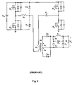
- FIG. 4 shows an exemplary embodiment for a converter in accordance with the present invention.
- FIG. 5 shows a simplified circuit diagram for the converter of FIG. 4 .
- FIGS. 6( a )–( e ) show topological stages during one half of the switching period of the converter of the invention: (a) topological stage [T 0 –T 1 ]; (b) topological stage [T 1 –T 2 ]; (c) topological stage [T 2 –T 3 ]; (d) topological stage [T 3 –T 4 ]; (e) topological stage [T 4 –T 5 ].
- FIGS. 7( a )–( n ) show key waveforms of the converter of this invention: (a) control signal for switch S 1 ; (b) control signal for switch S 2 ; (c) control signal for switch S 3 ; (d) control signal for switch S 3 ; (e) voltages V S1 and V S2 across switches S 1 and S 2 ; (f) voltages V S3 and V S4 across switches S 3 and S 4 ; (g) bridge voltage V AB ; (h) primary voltage V P of power transformer TR; (i) voltage v 2 of winding N 2 of auxiliary transformer TRA; (j) primary current i P of power transformer TR; (k) current i 2 through winding N 2 of auxiliary transformer TRA; (l) current i D1 through diode D 1 ; (m) current i D2 through diode D 2 ; (n) voltage v S at the input of output filter.
- FIG. 8 shows another exemplary embodiment of the converter of the present invention with two winding coupled inductors.
- FIG. 9 shows another implementation of the converter of FIG. 8 with three-winding coupled primary inductor.
- FIG. 10 shows yet another implementation of the converter of FIG. 8 with two-winding coupled primary inductor.
- FIG. 11 shows yet another implementation of the converter of the present invention with two-winding coupled primary inductor.
- FIG. 12 shows an example of the implementation of the converter of the invention where ZVS energy is stored in the leakage inductance of auxiliary transformer TRA.
- FIG. 13 shows an example of the implementation of the converter of the invention with power transformer TR connected directly across a bridge.
- FIG. 14 shows the implementation of the converter of the invention with winding N 1 of the auxiliary transformer connected to the midpoint of the leading leg of a bridge.
- FIG. 15 shows an example of the implementation of the converter of the invention with winding N 1 of the auxiliary transformer connected to a capacitive voltage divider.
- FIG. 16 shows the implementation of the converter of the invention with a current-doubler rectifier.
- FIG. 17 shows the implementation of the converter of the invention with a full-bridge, full-wave rectifier.
- FIG. 18 shows an example of the implementation of the converter of the invention with two transformers.
- FIG. 19 shows an example of the implementation of the converter of the invention with ZVS commutation circuits employed in two bridge legs.
- FIG. 20 shows another example of the implementation of the converter of the invention with ZVS commutation circuits employed in both bridge legs.
- FIG. 4 shows an exemplary embodiment for a converter in accordance with the present invention.
- the converter in FIG. 4 is a full bridge converter having an input port for receiving input power source V IN and an output port for supplying output power to load R L .
- the converter employs power transformer TR, auxiliary transformer TRA, and a bridge comprising leading-leg primary switches Q 1 and Q 2 and lagging-leg primary switches Q 3 and Q 4 , which are controllable switching devices.
- a controller regulates the load current by periodically switching controllable switching devices Q 1 , Q 2 , Q 3 and Q 4 into on and off states.
- Also included in the exemplary converter of the present invention is primary inductance L P , capacitor C B2 , primary diodes D 1 and D 2 , and blocking capacitor C B1 .
- the converter in FIG. 4 includes rectifiers D R1 and D R2 and a low pass filter comprising L f and C f .
- the present invention provides an isolated phase shift controlled full bridge converter that creates conditions for achieving ZVS, particularly for the leading-leg primary switches Q 1 and Q 2 under a wide range of load currents and with high power intensity.
- power transformer TR is used for the transfer of input power to the output of the converter, while auxiliary transformer TRA functions as an alternating energy source that isolates primary transformer TR from the switches and provides the needed energy for achieving ZVS.
- power transformer TR and auxiliary transformer TRA are connected to the leading and lagging legs of the full bridge such that a change in the phase shift between the two legs changes the volt-second product on the windings of power transformer TR and auxiliary transformer TRA. More specifically, a change in the phase shift between the two legs of the bridge increases the volt-second product on the windings of one transformer and decreases the volt-second product on the windings of the other transformer.
- the load is connected to the secondary winding(s) of power transformer TR whose volt-second product increases as the phase shift between the two legs increases.
- the primary of auxiliary transformer TRA is connected to the center tap of power transformer TR and ground through blocking capacitor C B1 , whereas its secondary is connected in series with the primary winding of power transformer TR and the leading leg of the bridge through primary inductor L P that is employed to store the needed energy supplied by auxiliary transformer TRA for zero-voltage switching of the bridge switches Q 1 and Q 2 .
- two diodes D 1 and D 2 are connected from the node connecting the primary of power transformer TR and the secondary of auxiliary transformer TRA to the positive and negative (ground) rail of the bridge to provide a path for the current through primary inductor L P .
- the phase shift between the bridge legs (comprising the leading-leg primary switches Q 1 and Q 2 and the lagging-leg primary switches Q 3 and Q 4 ) changes so that the volt-second product on the windings of power transformer TR also changes.
- the volt-second product on the windings of auxiliary transformer TRA changes, which changes the energy stored in the primary inductor L P. This is because the stored energy is proportional to the volt-second product of the secondary of auxiliary transformer TRA.
- primary inductor L P is connected in series with the leading-leg primary switches Q 1 and Q 2 for storing the energy supplied by the alternating energy source of the invention, i.e., auxiliary transformer TRA, to create the necessary conditions for switching these controllable switching devices at a substantially low voltage, e.g., substantially zero voltage, so as to avoid hard switching conditions.
- the present invention can achieve ZVS in a very wide range of input voltage and load current, including no load, with minimum circulating energy.
- the size of primary inductor L P can be minimized by properly selecting the turns ratio of auxiliary transformer TRA. Consequently, the size of primary inductor L P can be reduced compared to the prior art implementations.
- auxiliary transformer TRA does not need to store energy and is used as an alternating energy source for supplying energy to primary inductor L P , its size can be small. Also, because the sizes of primary inductor L P and auxiliary transformer TRA are determined by the converter's maximum output power through the selection of the bridge switches, in particular, their total output capacitance, the sizes of primary inductor L P and auxiliary transformer TRA do not change significantly as the maximum output power increases.
- the transformer's leakage inductance can also be minimized.
- the converter of the invention exhibits a relatively small duty-cycle loss, which minimizes both the conduction loss of the primary switches and the voltage stress on the components of the secondary side of power transformer TR, thereby improving conversion efficiency.
- the secondary-side parasitic ringing caused by a resonance between primary inductance L P and the junction capacitance of rectifier comprising D R1 or D R2 is also reduced and is effectively controlled by primary side diodes D 1 and D 2 , which are connected between the rails and the node connecting the primary of power transformer TR and the secondary of auxiliary transformer TRA.
- FIG. 5 shows its simplified circuit diagram.
- inductance of output filter L F is large enough so that during a switching cycle the output filter can be modeled as a constant current source with the magnitude equal to output current I O .
- the capacitance of capacitor C B2 is large enough so that the capacitor can be modeled as a constant voltage source. Because the average voltage of the windings of both transformers TR and TRA during a switching cycle must be zero and because when the phase-shift control is used, the pair of switches in each bridge leg operate with 50% duty cycle, the magnitude of the voltage sources that models C B2 is V IN /2.
- Blocking capacitor C B1 which is used to prevent the transformer core saturation due to various bridge component mismatching, can be neglected since it has no significant effect on the operation of the circuit.
- FIGS. 6( a )–( e ) show topological stages of the converter of this invention during a half of the switching period
- FIGS. 7( a )–( n ) show its key waveforms.
- FIG. 6( a ) when diagonal switches S 1 and S 4 are conducting, primary voltage V P is negative so that the load current is flowing through rectifier D R2 and the lower secondary of power transformer TR.
- lagging-lag switches S 3 and S 4 can achieve a complete ZVS turn on even at very light load currents because the energy for creating ZVS conditions is stored in large filter inductor Lf.
- Lf filter inductor
- E LP 1 2 ⁇ L P ⁇ i 2 2 , ( 4 )
- E LP must be at least equal to the energy required to charge up the capacitance of the leading-leg switch that is turning off to V IN and discharge the capacitance of the leading-leg switch that is about to be turned on to zero, i.e., E LP ⁇ 2 CV IN 2 .
- Expressions (10) and (11) can be used to estimate the required value of primary inductance L P and the turns ratio of auxiliary transformer n A .
- L P can be calculated as L P ⁇ 4 ⁇ CV IN ⁇ ( MAX ) 2 ( I O ⁇ ( MAX ) / n ) 2 , ( 12 ) where V IN(MAX) is the high line input voltage since it represents the worst-case input voltage.
- L P the smallest value of L P that satisfies (12) should be taken, i.e., L P ⁇ 4 ⁇ ⁇ C ⁇ ⁇ V IN ⁇ ⁇ ( MAX ) 2 ( I O ⁇ ( MAX ) / n ) 2 . ( 13 )
- n A n 1 4 ⁇ ⁇ f S ⁇ CL P .
- n A should be selected so that n A ⁇ 1 4 ⁇ ⁇ f S ⁇ CL P . ( 15 )
- the circuit of this invention achieves a complete ZVS in the entire load range, i.e., from full load down to no load.
- the value of primary inductance L P in the circuit of this invention is many times smaller than the value of primary inductance L P required to achieve ZVS of the primary switches in the conventional phase-shifted converter shown in FIG. 2 .
- the value of L P in the conventional converter L P(CONV) is determined by the condition that L P(CONV) has enough energy to achieve ZVS at the minimum desirable current, i.e., L P ⁇ ( CONV ) ⁇ 4 ⁇ ⁇ C ⁇ ⁇ V IN ⁇ ⁇ ( MAX ) 2 ( I O ⁇ ( MIN ) / n ) 2 , ( 16 ) where I O(MIN) is the minimum current at which complete ZVS can be achieved.
- L P(CONV) must be four times larger than L P in the circuit of this invention.
- L P(CONV) that is nine times larger than L P is required.
- the required value of L P(CONV) can be somewhat reduced by increasing the magnetizing current (reducing the magnetizing inductance) of the transformer, since the increased magnetizing current that flows through L P(CONV) increases the energy stored in L P(CONV) . Even with the optimally selected magnetizing inductance of the transformer, the required L P(CONV) is substantially larger than required L P in the circuit of this invention.
- the secondary-side duty-cycle loss of the circuit of this invention is also substantially reduced compared to that of the conventional full-bridge ZVS-PWM converter.
- the reduced value of L P reduces the energy in the parasitic ringing on the secondary side.
- this parasitic ringing is very much suppressed in the circuit in FIG. 4 because diodes D 1 and D 2 clamp the primary voltage of power transformer TR to the input voltage. Since the leakage of the power transformer in the circuit of this invention can be minimized because it is not used to store ZVS energy, the primary winding clamping also effectively clamps the secondary winding voltage. Any parasitic ringing due to the residual leakage inductance of the transformer can be controlled with a small (low-power) snubber circuit.
- FIGS. 8 through 11 show some of the implementations with primary inductor L P implemented as a two- or three-winding coupled inductor.
- the principle of operation of the circuits in FIGS. 8 through 11 is the same as that of the circuit in FIG. 4 .
- the circuit of this invention can be implemented without inductor L P , as shown in FIG. 12 .
- the energy required for ZVS of leading-leg switches is stored in the leakage inductance of auxiliary transformer TRA.
- auxiliary transformer TRA is designed with a proper value of the leakage inductance.
- the circuit of this invention can also be implemented as shown in FIG. 13 .
- power transformer TR is directly coupled across the bridge legs so that the reflected load current into the primary is not flowing through primary inductor L P .
- the secondary-side duty-cycle loss can virtually be eliminated.
- the circuits of this invention can also be implemented by connecting winding N 1 of auxiliary transformer TRA to any point in the circuit whose average voltage is V IN /2 instead of connecting it to the center tap of power transformer TR.
- An example of this implementation is shown in FIG. 14 .
- the only difference between the circuit in FIG. 14 and the circuit in FIG. 4 is that the amount of energy stored in primary inductor L P in the circuit in FIG. 14 is independent of the load current and input voltage since a constant volt-second product is applied across L P because, with the phase-shift control, the leading-leg switches always operate with 50% duty cycle.
- FIG. 15 shows another implementation of the circuit in FIG. 14 , where winding N 1 is connected to a capacitive divider that provides voltage V IN /2. Under this arrangement, the energy supplied by the alternating energy source is independent of current changes within the converter.
- FIG. 4 The converter of the invention shown in FIG. 4 and any of its variations can be implemented with any type of secondary-side rectifier.
- FIGS. 16 and 17 show implementations with a current doubler and a full-bridge full-wave rectifier, respectively.
- the circuits of this invention can also be implemented with multiple transformers as, for example, shown in FIG. 18 .
- the circuit of this invention can also be implemented with the described ZVS commutation network consisting of an auxiliary transformer and a primary inductance connected to each of the bridge legs, as shown in FIGS. 19 and 20 .
- the lagging-leg switches Q 3 and Q 4 use a ZVS commutation network to achieve ZVS in a wide load and input-voltage range.
- the lagging-leg switches Q 3 and Q 4 can use the energy stored in the output-filter inductor to create the ZVS conditions.
- circuit of this invention could also be implemented with a primary-side ZVS commutating network consisting of a primary inductor, an auxiliary transformer, and a pair of diodes connected to each of the bridge-legs.
- control of the circuits of this invention is the same as the control of any other constant-frequency FB ZVS converter.
- any of the integrated phase-shift controllers or PMW controllers available on the market can be used to implement the control of the proposed circuit.
Landscapes
- Engineering & Computer Science (AREA)
- Power Engineering (AREA)
- Dc-Dc Converters (AREA)
Abstract
Description
so that current i2 is
since LP>>LLK.
Where i2 is the value of i2 at the moment of turn off of a leading-leg switch, i.e., at t=T3 and t=T7 in
substituting expression (1) for iD1 and iD2 into (4) and recognizing that iD1 and iD2 flow only during the off time (1−D)TS, as shown in
where fS=1/TS is the switching frequency.
E LP≧2CV IN 2. (8)
where VIN(MAX) is the high line input voltage since it represents the worst-case input voltage. To minimize amount of the full load circulating energy and the size of inductor LP, the smallest value of LP that satisfies (12) should be taken, i.e.,
where IO(MIN) is the minimum current at which complete ZVS can be achieved.
Claims (25)
Priority Applications (2)
| Application Number | Priority Date | Filing Date | Title |
|---|---|---|---|
| US10/644,906 US6992902B2 (en) | 2003-08-21 | 2003-08-21 | Full bridge converter with ZVS via AC feedback |
| PCT/US2004/027355 WO2005022732A2 (en) | 2003-08-21 | 2004-08-23 | Full bridge power converters with zero-voltage switching |
Applications Claiming Priority (1)
| Application Number | Priority Date | Filing Date | Title |
|---|---|---|---|
| US10/644,906 US6992902B2 (en) | 2003-08-21 | 2003-08-21 | Full bridge converter with ZVS via AC feedback |
Publications (2)
| Publication Number | Publication Date |
|---|---|
| US20050041439A1 US20050041439A1 (en) | 2005-02-24 |
| US6992902B2 true US6992902B2 (en) | 2006-01-31 |
Family
ID=34194189
Family Applications (1)
| Application Number | Title | Priority Date | Filing Date |
|---|---|---|---|
| US10/644,906 Expired - Lifetime US6992902B2 (en) | 2003-08-21 | 2003-08-21 | Full bridge converter with ZVS via AC feedback |
Country Status (2)
| Country | Link |
|---|---|
| US (1) | US6992902B2 (en) |
| WO (1) | WO2005022732A2 (en) |
Cited By (28)
| Publication number | Priority date | Publication date | Assignee | Title |
|---|---|---|---|---|
| US20050047176A1 (en) * | 2002-09-30 | 2005-03-03 | Kenichi Fukumoto | Dc/ac conversion device and ac power supply method |
| US20050269998A1 (en) * | 2002-11-29 | 2005-12-08 | Rohm Co., Ltd. | DC-AC converter and controller IC therefor |
| US20060018139A1 (en) * | 2004-07-22 | 2006-01-26 | Valeo Electrical System, Inc. | Zero-crossing correction in sinusoidally commutated motors |
| US7116568B1 (en) * | 2003-07-28 | 2006-10-03 | The United States Of America As Represented By The Administrator Of The National Aeronautics And Space Administration | Series connected buck-boost regulator |
| US7227762B1 (en) * | 2006-05-15 | 2007-06-05 | Pi International Ltd. | Fine-tuning circuit for the winding voltage of a transformer |
| US20070171684A1 (en) * | 2004-03-05 | 2007-07-26 | Rohm Company, Ltd. | Dc-ac converter controller, ic therefor, and electronic apparatus utilizing such dc-ac converter |
| US20080031028A1 (en) * | 2002-11-29 | 2008-02-07 | Rohm Co., Ltd. | DC-AC Converter and Controller IC Thereof |
| US20080130334A1 (en) * | 2003-06-19 | 2008-06-05 | Koninlijke Philips Electronics N.V. | Determining Reflected Power |
| US20080170418A1 (en) * | 2005-06-29 | 2008-07-17 | Takayoshi Nishiyama | Dc-dc converter |
| US20090026968A1 (en) * | 2007-07-23 | 2009-01-29 | Huettinger Elektronik Gmbh + Co. Kg | Plasma supply device |
| US20090196072A1 (en) * | 2007-12-03 | 2009-08-06 | Zhong Ye | Phase-shifted dual-bridge DC/DC converter with wide-range ZVS and zero circulating current |
| US20090244944A1 (en) * | 2008-03-25 | 2009-10-01 | Delta Electronics, Inc. | Power converter system that operates efficiently over a range of load conditions |
| US20100182803A1 (en) * | 2009-01-21 | 2010-07-22 | Zhanghe Nan | Resonant converter equipped with a phase shifting output circuit |
| US20100246231A1 (en) * | 2009-03-31 | 2010-09-30 | TDK-Lambba Americas Inc. | Achieving zvs in a two quadrant converter using a simplified auxiliary circuit |
| US20110007528A1 (en) * | 2008-03-06 | 2011-01-13 | Koninklijke Philips Electronics N.V. | Method for controlling a switching device of a resonant power converter, especially in order to provide a required power, especially for an x-ray generator |
| KR101025987B1 (en) | 2009-09-14 | 2011-03-30 | 삼성전기주식회사 | Power supply apparatus supplying additional current to power converting switch |
| KR101104402B1 (en) | 2010-05-04 | 2012-01-16 | 주식회사 팩테크 | Method and Apparatus for Controlling Phase-Shift DC/DC Full-Bridge Converter |
| KR101245520B1 (en) | 2011-07-27 | 2013-03-21 | 한국전기연구원 | Symmetric and Bidirectional Resonant Converter |
| TWI397249B (en) * | 2009-01-05 | 2013-05-21 | Spi Electronic Co Ltd | Resonant converter with phase shift output path |
| US20130301306A1 (en) * | 2011-01-26 | 2013-11-14 | Murata Manufacturing Co., Ltd. | Switching power supply device |
| US20140157015A1 (en) * | 2011-08-12 | 2014-06-05 | Intersil Americas Inc. | Clamp circuits for power converters |
| US20140177282A1 (en) * | 2012-12-21 | 2014-06-26 | Korea Advanced Institute Of Science And Technology | Power supply device |
| KR101428392B1 (en) | 2013-05-31 | 2014-08-08 | 현대자동차주식회사 | Full bridge DC-DC converter with current doubler |
| US20160352234A1 (en) * | 2015-05-12 | 2016-12-01 | Tdk Corporation | Resonant converter and switching power supply device |
| TWI635697B (en) * | 2017-08-01 | 2018-09-11 | 崑山科技大學 | Interleaved high-step-up zero-voltage switching dc-dc converter |
| US20190020281A1 (en) * | 2016-03-15 | 2019-01-17 | Abb Schweiz Ag | Bidirectional dc-dc converter and control method therefor |
| TWI651922B (en) * | 2017-11-29 | 2019-02-21 | 國家中山科學研究院 | Non-isolated transformer type single-phase converter |
| TWI719877B (en) * | 2019-06-12 | 2021-02-21 | 台達電子工業股份有限公司 | Isolated converter with high boost ratio |
Families Citing this family (35)
| Publication number | Priority date | Publication date | Assignee | Title |
|---|---|---|---|---|
| DE102004050665A1 (en) * | 2004-10-18 | 2006-05-04 | Mk-Elektronik-Gmbh | Electronic power supply |
| GB0427682D0 (en) * | 2004-12-17 | 2005-01-19 | Havard Engineering Plc | Power control |
| US7554820B2 (en) * | 2005-09-20 | 2009-06-30 | Harman International Industries, Incorporated | Series resonant DC-DC converter |
| US20070109822A1 (en) * | 2005-11-14 | 2007-05-17 | Kan-Sheng Kuan | Zero voltage switch method for synchronous rectifier and inverter |
| NZ550043A (en) * | 2006-09-21 | 2008-01-31 | Eaton Power Quality Company | A switched mode power supply and method of production |
| US7660135B2 (en) * | 2007-05-23 | 2010-02-09 | Hamilton Sundstrand Corporation | Universal AC high power inveter with galvanic isolation for linear and non-linear loads |
| US7869237B1 (en) | 2007-12-27 | 2011-01-11 | Lockheed Martin Corporation | Phase-shifted bridge with auxiliary circuit to maintain zero-voltage-switching |
| TWI362168B (en) * | 2007-12-28 | 2012-04-11 | Ind Tech Res Inst | Resonance circuit adapted for h-bridge dc-dc converter and a method for adapting the same for operating in boost/buck mode |
| TWI371910B (en) * | 2008-05-02 | 2012-09-01 | Chimei Innolux Corp | Inverter circuit |
| KR100966972B1 (en) | 2008-07-17 | 2010-06-30 | 삼성전기주식회사 | Variable switching frequency type power supply |
| US7859870B1 (en) | 2008-07-29 | 2010-12-28 | Lockheed Martin Corporation | Voltage clamps for energy snubbing |
| US8035996B1 (en) * | 2009-04-16 | 2011-10-11 | Intersil Americas Inc. | Asymmetric zero-voltage switching full-bridge power converters |
| JP5640464B2 (en) * | 2009-07-29 | 2014-12-17 | Tdk株式会社 | Switching power supply |
| JP5558631B2 (en) * | 2011-04-18 | 2014-07-23 | 三菱電機株式会社 | Power conversion device and in-vehicle power supply device including the same |
| US9088222B2 (en) * | 2011-11-17 | 2015-07-21 | Qualcomm Incorporated | Systems, methods, and apparatus for a high power factor single phase rectifier |
| CN102570872A (en) * | 2012-02-23 | 2012-07-11 | 石家庄通合电子有限公司 | Single-phase grid-connection inverter circuit |
| SE536532C2 (en) * | 2012-03-23 | 2014-02-04 | Nordic Light Ab | Electronic driver for gas discharge lamp and method in one such driver |
| US9389288B2 (en) | 2012-09-14 | 2016-07-12 | General Electric Company | System and method for maintaining soft switching condition in a gradient coil driver circuit |
| US9391532B2 (en) * | 2013-03-14 | 2016-07-12 | Infineon Technologies Ag | System and method for a switched-mode power converter |
| CN103441680B (en) * | 2013-08-13 | 2015-12-23 | 陈仲 | A kind of soft switching full-bridge direct-current converter reducing circulation loss |
| TWI501529B (en) | 2013-12-06 | 2015-09-21 | Ind Tech Res Inst | Dc-dc power conversion apparatus and method |
| US9590531B2 (en) * | 2014-02-14 | 2017-03-07 | Majid Pahlevaninezhad | ZVS voltage source inverter with reduced output current ripple |
| CN103916017A (en) * | 2014-03-17 | 2014-07-09 | 陕西科技大学 | DC convertor with wide voltage range and wide load range |
| DE102014210325A1 (en) * | 2014-06-02 | 2015-12-03 | Robert Bosch Gmbh | Voltage transformer and method |
| JP6009003B2 (en) * | 2015-01-20 | 2016-10-19 | 三菱電機株式会社 | DC / DC converter |
| US9705411B2 (en) * | 2015-12-08 | 2017-07-11 | Delta Electronics, Inc. | Soft-switched bidirectional buck-boost converters |
| CN105811779B (en) * | 2016-04-25 | 2018-08-28 | 天津大学 | CLTC resonant type soft-switch reversible transducers |
| CN108111024A (en) * | 2018-01-24 | 2018-06-01 | 深圳市英能达电子有限公司 | A kind of switching power circuit and its Switching Power Supply |
| TWI692189B (en) * | 2019-01-31 | 2020-04-21 | 宏碁股份有限公司 | Power conversion device |
| US10797581B1 (en) * | 2019-03-25 | 2020-10-06 | Semiconductor Components Industries, Llc | Power supply system for controlling a ZVS parameter to optimize efficiency using artificial intelligence |
| CN110932557B (en) * | 2019-11-29 | 2021-01-12 | 山东科技大学 | High-gain quasi-resonant DC-DC converter based on voltage doubling rectifying circuit |
| CN112737345B (en) * | 2020-12-29 | 2022-06-14 | 陕西科技大学 | Control method of wide-load-range zero-voltage switch phase-shifted full-bridge converter |
| CN115378266A (en) | 2021-05-19 | 2022-11-22 | 台达电子企业管理(上海)有限公司 | Converter suitable for wide-range output voltage and control method thereof |
| CN115378265A (en) * | 2021-05-19 | 2022-11-22 | 台达电子企业管理(上海)有限公司 | Converter suitable for wide-range output voltage and control method thereof |
| CN117200587B (en) * | 2023-11-08 | 2024-02-02 | 中山市宝利金电子有限公司 | Low-power-loss charging pile circuit based on direct power transmission and charging pile |
Citations (2)
| Publication number | Priority date | Publication date | Assignee | Title |
|---|---|---|---|---|
| US5563775A (en) * | 1994-06-16 | 1996-10-08 | Reliance Comm/Tech Corporation | Full bridge phase displaced resonant transition circuit for obtaining constant resonant transition current from 0° phase angle to 180° phase angle |
| US6356462B1 (en) * | 2000-08-31 | 2002-03-12 | Delta Electronics, Inc. | Soft-switched full-bridge converters |
-
2003
- 2003-08-21 US US10/644,906 patent/US6992902B2/en not_active Expired - Lifetime
-
2004
- 2004-08-23 WO PCT/US2004/027355 patent/WO2005022732A2/en active Application Filing
Patent Citations (2)
| Publication number | Priority date | Publication date | Assignee | Title |
|---|---|---|---|---|
| US5563775A (en) * | 1994-06-16 | 1996-10-08 | Reliance Comm/Tech Corporation | Full bridge phase displaced resonant transition circuit for obtaining constant resonant transition current from 0° phase angle to 180° phase angle |
| US6356462B1 (en) * | 2000-08-31 | 2002-03-12 | Delta Electronics, Inc. | Soft-switched full-bridge converters |
Cited By (76)
| Publication number | Priority date | Publication date | Assignee | Title |
|---|---|---|---|---|
| US7589981B2 (en) | 2002-09-30 | 2009-09-15 | Rohm Co., Ltd. | DC-AC converter and method of supplying AC power |
| US7403401B2 (en) | 2002-09-30 | 2008-07-22 | Rohm Co., Ltd. | DC-AC converter and method of supplying AC power |
| US20050047176A1 (en) * | 2002-09-30 | 2005-03-03 | Kenichi Fukumoto | Dc/ac conversion device and ac power supply method |
| US7095632B2 (en) * | 2002-09-30 | 2006-08-22 | Rohm Co., Ltd. | Dc/ac conversion device and ac power supply method |
| US20080285321A1 (en) * | 2002-09-30 | 2008-11-20 | Rohm Co., Ltd. | DC-AC Converter and Method of Supplying AC Power |
| US20080037291A1 (en) * | 2002-09-30 | 2008-02-14 | Rohm Co., Ltd. | DC-AC Converter and Method of Supplying AC Power |
| US20060239038A1 (en) * | 2002-09-30 | 2006-10-26 | Rohm Co., Ltd. | DC-AC converter and method of supplying AC power |
| US7272022B2 (en) | 2002-09-30 | 2007-09-18 | Rohm Co., Ltd. | DC-AC converter and method of supplying AC power |
| US7835161B2 (en) | 2002-09-30 | 2010-11-16 | Rohm Co., Ltd. | DC-AC converter and method of supplying AC power |
| US20100014336A1 (en) * | 2002-09-30 | 2010-01-21 | Rohm Co., Ltd. | DC-AC Converter and Method of Supplying AC Power |
| US7099168B2 (en) * | 2002-11-29 | 2006-08-29 | Rohm Co., Ltd. | DC-AC converter and controller IC therefor |
| US20060245220A1 (en) * | 2002-11-29 | 2006-11-02 | Rohm Co., Ltd. | DC-AC converter and controller IC therefor |
| US7292463B2 (en) | 2002-11-29 | 2007-11-06 | Rohm Co., Ltd. | DC-AC converter and controller IC therefor |
| US20080031028A1 (en) * | 2002-11-29 | 2008-02-07 | Rohm Co., Ltd. | DC-AC Converter and Controller IC Thereof |
| US7492620B2 (en) | 2002-11-29 | 2009-02-17 | Rohm Co., Ltd. | DC-AC converter and controller IC thereof |
| US20050269998A1 (en) * | 2002-11-29 | 2005-12-08 | Rohm Co., Ltd. | DC-AC converter and controller IC therefor |
| US20080130334A1 (en) * | 2003-06-19 | 2008-06-05 | Koninlijke Philips Electronics N.V. | Determining Reflected Power |
| US7417876B2 (en) * | 2003-06-19 | 2008-08-26 | Nxp B.V. | Determining reflected power |
| US7116568B1 (en) * | 2003-07-28 | 2006-10-03 | The United States Of America As Represented By The Administrator Of The National Aeronautics And Space Administration | Series connected buck-boost regulator |
| US20090072754A1 (en) * | 2004-03-05 | 2009-03-19 | Rohm Co., Ltd. | Dc-ac converter, controller ic therefor, and electronic apparatus utilizing such dc-ac converter |
| US20070171684A1 (en) * | 2004-03-05 | 2007-07-26 | Rohm Company, Ltd. | Dc-ac converter controller, ic therefor, and electronic apparatus utilizing such dc-ac converter |
| US7466566B2 (en) * | 2004-03-05 | 2008-12-16 | Rohm Co., Ltd. | DC-AC converter, controller IC therefor, and electronic apparatus utilizing such DC-AC converter |
| US7920390B2 (en) * | 2004-03-05 | 2011-04-05 | Rohm Co., Ltd. | DC-AC converter, controller IC therefor, and electronic apparatus utilizing such DC-AC converter |
| US20060018139A1 (en) * | 2004-07-22 | 2006-01-26 | Valeo Electrical System, Inc. | Zero-crossing correction in sinusoidally commutated motors |
| US7161819B2 (en) * | 2004-07-22 | 2007-01-09 | Valeo Electrical Systems, Inc. | Zero-crossing correction in sinusoidally commutated motors |
| US20080170418A1 (en) * | 2005-06-29 | 2008-07-17 | Takayoshi Nishiyama | Dc-dc converter |
| US7227762B1 (en) * | 2006-05-15 | 2007-06-05 | Pi International Ltd. | Fine-tuning circuit for the winding voltage of a transformer |
| US8129653B2 (en) | 2007-07-23 | 2012-03-06 | Huettinger Elektronik Gmbh + Co. Kg | Plasma supply device |
| US20090027936A1 (en) * | 2007-07-23 | 2009-01-29 | Huettinger Elektronik Gmbh + Co. Kg | Rf power supply |
| US8466622B2 (en) | 2007-07-23 | 2013-06-18 | Huettinger Elektronik Gmbh + Co. Kg | High frequency power supply |
| US8436543B2 (en) | 2007-07-23 | 2013-05-07 | Huettinger Elektronik Gmbh + Co. Kg | Plasma supply device |
| US20090026181A1 (en) * | 2007-07-23 | 2009-01-29 | Huettinger Elektronik Gmbh + Co. Kg | Radio frequency power supply |
| US20100171427A1 (en) * | 2007-07-23 | 2010-07-08 | Huettinger Elektronik Gmbh + Co. Kg | Protecting High-Frequency Amplifers |
| US20100170640A1 (en) * | 2007-07-23 | 2010-07-08 | Huettinger Elektronik Gmbh + Co. Kg | Determining high frequency operating parameters in a plasma system |
| US20100171428A1 (en) * | 2007-07-23 | 2010-07-08 | Huettinger Elektronik Gmbh + Co. Kg | Driving switches of a plasma load power suuply |
| US8222885B2 (en) | 2007-07-23 | 2012-07-17 | Huettinger Elektronik Gmbh + Co. Kg | Isolating a control signal source in a high frequency power supply |
| US20100194280A1 (en) * | 2007-07-23 | 2010-08-05 | Huettinger Elektronik Gmbh + Co. Kg | Plasma Supply Device |
| US8866400B2 (en) | 2007-07-23 | 2014-10-21 | Trumpf Huettinger Gmbh + Co. Kg | Plasma supply device |
| US8357874B2 (en) | 2007-07-23 | 2013-01-22 | Huettinger Elektronik Gmbh + Co. Kg | Radio frequency power supply |
| US8421377B2 (en) | 2007-07-23 | 2013-04-16 | Huettinger Elektronik Gmbh + Co. Kg | Protecting high-frequency amplifers |
| US8482205B2 (en) | 2007-07-23 | 2013-07-09 | Huettinger Elektronik Gmbh + Co. Kg | Driving switches of a plasma load power supply |
| US8643279B2 (en) | 2007-07-23 | 2014-02-04 | Huettinger Elektronik Gmbh + Co. Kg | Determining high frequency operating parameters in a plasma system |
| US20090026964A1 (en) * | 2007-07-23 | 2009-01-29 | Huettinger Elektronik Gmbh + Co. Kg | High Frequency Power Supply |
| US20090027937A1 (en) * | 2007-07-23 | 2009-01-29 | Huettinger Elektronik Gmbh + Co. Kg | High frequency power supply |
| US20090026968A1 (en) * | 2007-07-23 | 2009-01-29 | Huettinger Elektronik Gmbh + Co. Kg | Plasma supply device |
| US8154897B2 (en) | 2007-07-23 | 2012-04-10 | Huettinger Elektronik Gmbh + Co. Kg | RF power supply |
| US20090196072A1 (en) * | 2007-12-03 | 2009-08-06 | Zhong Ye | Phase-shifted dual-bridge DC/DC converter with wide-range ZVS and zero circulating current |
| US9118259B2 (en) * | 2007-12-03 | 2015-08-25 | Texas Instruments Incorporated | Phase-shifted dual-bridge DC/DC converter with wide-range ZVS and zero circulating current |
| US20110007528A1 (en) * | 2008-03-06 | 2011-01-13 | Koninklijke Philips Electronics N.V. | Method for controlling a switching device of a resonant power converter, especially in order to provide a required power, especially for an x-ray generator |
| US8446744B2 (en) * | 2008-03-06 | 2013-05-21 | Koninklijke Philips Electronics N.V. | Method for controlling a switching device of a resonant power converter, especially in order to provide a required power, especially for an X-ray generator |
| US8179698B2 (en) * | 2008-03-25 | 2012-05-15 | Delta Electronics, Inc. | Power converter system that operates efficiently over a range of load conditions |
| TWI450482B (en) * | 2008-03-25 | 2014-08-21 | Delta Electronics Inc | A power converter system that operates efficiently over a range of load conditions |
| US20090244944A1 (en) * | 2008-03-25 | 2009-10-01 | Delta Electronics, Inc. | Power converter system that operates efficiently over a range of load conditions |
| TWI397249B (en) * | 2009-01-05 | 2013-05-21 | Spi Electronic Co Ltd | Resonant converter with phase shift output path |
| US8587963B2 (en) | 2009-01-21 | 2013-11-19 | Fsp Technology Inc. | Resonant converter equipped with multiple output circuits to provide multiple power outlets |
| US20100182803A1 (en) * | 2009-01-21 | 2010-07-22 | Zhanghe Nan | Resonant converter equipped with a phase shifting output circuit |
| US7869226B2 (en) | 2009-03-31 | 2011-01-11 | Tdk-Lambda Americas Inc. | Achieving ZVS in a two quadrant converter using a simplified auxiliary circuit |
| US20100246231A1 (en) * | 2009-03-31 | 2010-09-30 | TDK-Lambba Americas Inc. | Achieving zvs in a two quadrant converter using a simplified auxiliary circuit |
| KR101025987B1 (en) | 2009-09-14 | 2011-03-30 | 삼성전기주식회사 | Power supply apparatus supplying additional current to power converting switch |
| KR101104402B1 (en) | 2010-05-04 | 2012-01-16 | 주식회사 팩테크 | Method and Apparatus for Controlling Phase-Shift DC/DC Full-Bridge Converter |
| US20130301306A1 (en) * | 2011-01-26 | 2013-11-14 | Murata Manufacturing Co., Ltd. | Switching power supply device |
| US9660536B2 (en) * | 2011-01-26 | 2017-05-23 | Murata Manufacturing Coo., Ltd. | Switching power supply device performs power transmission by using resonance phenomenon |
| KR101245520B1 (en) | 2011-07-27 | 2013-03-21 | 한국전기연구원 | Symmetric and Bidirectional Resonant Converter |
| US20140157015A1 (en) * | 2011-08-12 | 2014-06-05 | Intersil Americas Inc. | Clamp circuits for power converters |
| US8966294B2 (en) * | 2011-08-12 | 2015-02-24 | Intersil Americas LLC | Clamp circuits for power converters |
| US20140177282A1 (en) * | 2012-12-21 | 2014-06-26 | Korea Advanced Institute Of Science And Technology | Power supply device |
| US9112424B2 (en) * | 2012-12-21 | 2015-08-18 | Samsung Electro-Mechanics Co., Ltd. | Power supply device having improved power conversion efficiency in light load conditions |
| US9042123B2 (en) | 2013-05-31 | 2015-05-26 | Hyundai Motor Company | Full bridge DC-DC converter that applies current doubler |
| KR101428392B1 (en) | 2013-05-31 | 2014-08-08 | 현대자동차주식회사 | Full bridge DC-DC converter with current doubler |
| US20160352234A1 (en) * | 2015-05-12 | 2016-12-01 | Tdk Corporation | Resonant converter and switching power supply device |
| US9948198B2 (en) * | 2015-05-12 | 2018-04-17 | Tdk Corporation | Resonant converter and switching power supply device |
| US20190020281A1 (en) * | 2016-03-15 | 2019-01-17 | Abb Schweiz Ag | Bidirectional dc-dc converter and control method therefor |
| US10396676B2 (en) * | 2016-03-15 | 2019-08-27 | Abb Schweiz Ag | Bidirectional DC-DC converter and control method therefor |
| TWI635697B (en) * | 2017-08-01 | 2018-09-11 | 崑山科技大學 | Interleaved high-step-up zero-voltage switching dc-dc converter |
| TWI651922B (en) * | 2017-11-29 | 2019-02-21 | 國家中山科學研究院 | Non-isolated transformer type single-phase converter |
| TWI719877B (en) * | 2019-06-12 | 2021-02-21 | 台達電子工業股份有限公司 | Isolated converter with high boost ratio |
Also Published As
| Publication number | Publication date |
|---|---|
| US20050041439A1 (en) | 2005-02-24 |
| WO2005022732A3 (en) | 2005-06-02 |
| WO2005022732A2 (en) | 2005-03-10 |
Similar Documents
| Publication | Publication Date | Title |
|---|---|---|
| US6992902B2 (en) | Full bridge converter with ZVS via AC feedback | |
| US6356462B1 (en) | Soft-switched full-bridge converters | |
| Jang et al. | A new PWM ZVS full-bridge converter | |
| US4857822A (en) | Zero-voltage-switched multi-resonant converters including the buck and forward type | |
| US6353547B1 (en) | Three-level soft-switched converters | |
| Jang et al. | A new family of full-bridge ZVS converters | |
| Jang et al. | A new ZVS-PWM full-bridge converter | |
| Huber et al. | Single-stage, single-switch, isolated power supply technique with input-current shaping and fast output-voltage regulation for universal input-voltage-range applications | |
| US6239584B1 (en) | Two-inductor boost converter | |
| US5448467A (en) | Electrical power converter circuit | |
| US5434768A (en) | Fixed frequency converter switching at zero voltage | |
| US7269034B2 (en) | High efficiency power converter | |
| US7564702B2 (en) | High efficiency power converter | |
| US4788634A (en) | Resonant forward converter | |
| US7254047B2 (en) | Power converters having output capacitor resonant with autotransformer leakage inductance | |
| JP2875879B2 (en) | DC / DC switching converter circuit | |
| US7869237B1 (en) | Phase-shifted bridge with auxiliary circuit to maintain zero-voltage-switching | |
| US7136294B2 (en) | Soft switched zero voltage transition full bridge converter | |
| US8184458B2 (en) | Power converter load line control | |
| US7209370B2 (en) | Circuit for reducing losses at light load in a soft switching full bridge converter | |
| Kutkut | A full bridge soft switched telecom power supply with a current doubler rectifier | |
| JP2002101655A (en) | Switching power supply device | |
| US5870291A (en) | Asymmetrical half-bridge converter having adjustable parasitic resistances to offset output voltage DC bias | |
| US6812679B2 (en) | High efficiency AC-DC converter with power factor corrector | |
| Aydemir et al. | A critical evaluation of high power hard and soft switched isolated DC-DC converters |
Legal Events
| Date | Code | Title | Description |
|---|---|---|---|
| AS | Assignment |
Owner name: DELTA ELECTRONICS, INC., TAIWAN Free format text: ASSIGNMENT OF ASSIGNORS INTEREST;ASSIGNORS:JANG, YUNGTAEK;JOVANOVIC, MILAN M.;REEL/FRAME:014432/0100 Effective date: 20030819 |
|
| STCF | Information on status: patent grant |
Free format text: PATENTED CASE |
|
| FPAY | Fee payment |
Year of fee payment: 4 |
|
| FEPP | Fee payment procedure |
Free format text: PAYOR NUMBER ASSIGNED (ORIGINAL EVENT CODE: ASPN); ENTITY STATUS OF PATENT OWNER: LARGE ENTITY |
|
| FPAY | Fee payment |
Year of fee payment: 8 |
|
| FEPP | Fee payment procedure |
Free format text: MAINTENANCE FEE REMINDER MAILED (ORIGINAL EVENT CODE: REM.) |
|
| FEPP | Fee payment procedure |
Free format text: 11.5 YR SURCHARGE- LATE PMT W/IN 6 MO, LARGE ENTITY (ORIGINAL EVENT CODE: M1556) |
|
| MAFP | Maintenance fee payment |
Free format text: PAYMENT OF MAINTENANCE FEE, 12TH YEAR, LARGE ENTITY (ORIGINAL EVENT CODE: M1553) Year of fee payment: 12 |