US6937115B2 - Filter having parasitic inductance cancellation - Google Patents
Filter having parasitic inductance cancellation Download PDFInfo
- Publication number
- US6937115B2 US6937115B2 US10/082,616 US8261602A US6937115B2 US 6937115 B2 US6937115 B2 US 6937115B2 US 8261602 A US8261602 A US 8261602A US 6937115 B2 US6937115 B2 US 6937115B2
- Authority
- US
- United States
- Prior art keywords
- inductance
- coupled
- capacitor
- windings
- coupled windings
- Prior art date
- Legal status (The legal status is an assumption and is not a legal conclusion. Google has not performed a legal analysis and makes no representation as to the accuracy of the status listed.)
- Expired - Lifetime
Links
Images


Classifications
-
- H—ELECTRICITY
- H03—ELECTRONIC CIRCUITRY
- H03H—IMPEDANCE NETWORKS, e.g. RESONANT CIRCUITS; RESONATORS
- H03H7/00—Multiple-port networks comprising only passive electrical elements as network components
- H03H7/01—Frequency selective two-port networks
- H03H7/17—Structural details of sub-circuits of frequency selective networks
- H03H7/1741—Comprising typical LC combinations, irrespective of presence and location of additional resistors
- H03H7/1766—Parallel LC in series path
-
- H—ELECTRICITY
- H03—ELECTRONIC CIRCUITRY
- H03H—IMPEDANCE NETWORKS, e.g. RESONANT CIRCUITS; RESONATORS
- H03H7/00—Multiple-port networks comprising only passive electrical elements as network components
- H03H7/01—Frequency selective two-port networks
- H03H7/0115—Frequency selective two-port networks comprising only inductors and capacitors
-
- H—ELECTRICITY
- H03—ELECTRONIC CIRCUITRY
- H03H—IMPEDANCE NETWORKS, e.g. RESONANT CIRCUITS; RESONATORS
- H03H7/00—Multiple-port networks comprising only passive electrical elements as network components
- H03H7/01—Frequency selective two-port networks
- H03H7/17—Structural details of sub-circuits of frequency selective networks
- H03H7/1708—Comprising bridging elements, i.e. elements in a series path without own reference to ground and spanning branching nodes of another series path
-
- H—ELECTRICITY
- H03—ELECTRONIC CIRCUITRY
- H03H—IMPEDANCE NETWORKS, e.g. RESONANT CIRCUITS; RESONATORS
- H03H1/00—Constructional details of impedance networks whose electrical mode of operation is not specified or applicable to more than one type of network
- H03H2001/0021—Constructional details
- H03H2001/0042—Wound, ring or feed-through type capacitor
-
- H—ELECTRICITY
- H03—ELECTRONIC CIRCUITRY
- H03H—IMPEDANCE NETWORKS, e.g. RESONANT CIRCUITS; RESONATORS
- H03H1/00—Constructional details of impedance networks whose electrical mode of operation is not specified or applicable to more than one type of network
- H03H2001/0021—Constructional details
- H03H2001/005—Wound, ring or feed-through type inductor
-
- H—ELECTRICITY
- H03—ELECTRONIC CIRCUITRY
- H03H—IMPEDANCE NETWORKS, e.g. RESONANT CIRCUITS; RESONATORS
- H03H1/00—Constructional details of impedance networks whose electrical mode of operation is not specified or applicable to more than one type of network
- H03H2001/0021—Constructional details
- H03H2001/0078—Constructional details comprising spiral inductor on a substrate
-
- H—ELECTRICITY
- H03—ELECTRONIC CIRCUITRY
- H03H—IMPEDANCE NETWORKS, e.g. RESONANT CIRCUITS; RESONATORS
- H03H1/00—Constructional details of impedance networks whose electrical mode of operation is not specified or applicable to more than one type of network
- H03H2001/0021—Constructional details
- H03H2001/0085—Multilayer, e.g. LTCC, HTCC, green sheets
-
- H—ELECTRICITY
- H03—ELECTRONIC CIRCUITRY
- H03H—IMPEDANCE NETWORKS, e.g. RESONANT CIRCUITS; RESONATORS
- H03H7/00—Multiple-port networks comprising only passive electrical elements as network components
- H03H7/01—Frequency selective two-port networks
- H03H7/09—Filters comprising mutual inductance
Definitions
- the present invention relates generally to electrical components and filters and, more particularly, to components and filters for suppressing electrical signals.
- the attenuation of a filter stage can be determined by the amount of impedance mismatch between the series and shunt paths. For a low-pass filter, it is generally desirable to minimize shunt-path impedance and maximize series-path impedance at high frequencies.
- FIG. 2 shows a prior art first order model for a conventional filter capacitor C F including the equivalent series resistance (ESR), R ESR and equivalent series inductance (ESL), L ESL , of the capacitor.
- FIG. 3 illustrates the impedance characteristic of a typical prior art capacitor across frequency. As can be seen, at higher frequencies the capacitor impedance is dominated by the ESL. For example, a typical aluminum electrolytic capacitor may appear inductive (impedance rising with frequency) at frequencies above 50-100 kHz, thereby limiting its ability to shunt ripple at high frequencies.
- One prior-art approach for overcoming filter capacitor limitations is to couple capacitors of different types in parallel (to cover different frequency ranges) and/or to increase the order of the filter used (e.g., by adding series filter elements such as inductors). While these approaches can reduce parasitic effects to some extent, they can add considerable size, complexity, and cost to the filter.
- the present invention provides an electrical component that cancels the effect of the series inductance of a capacitive element or other element or circuit.
- a low-pass filter including an electrical component in the shunt path with inductance cancellation provides enhanced performance over frequency by maintaining a relatively low shunt path impedance out to relatively high frequencies.
- the invention is primarily shown and described in conjunction with electrical filters, it is understood that the invention is applicable to a wide variety of circuits, including power converters, transient suppressors, and sensors, e.g., resistive current sensors, in which it is desirable to cancel the inductance of a component or circuit.
- the shunt path impedance is typically the focus for common low-pass filters, in a high-pass filter, the series-path (of the filter) impedance may be considered to a greater extent.
- parasitic inductance is not limited to a particular component or element since the parasitic inductance of other parts of the circuit (e.g., wiring) may also be addressed with the inventive inductance cancellation technique.
- a component in one aspect of the invention, includes a capacitor connected to coupled windings for nullifying series inductance associated with the capacitor.
- the coupled windings provide an inductive impedance that cancels an inductive impedance of the capacitor, which can be referred to as an equivalent series inductance of the capacitor.
- a filter in another aspect of the invention, includes a component having a capacitive element and capacitive-path inductance cancellation provided by coupled windings.
- the coupled windings cancel the equivalent series inductance of the capacitor so as to enhance the filter performance over frequency.
- FIG. 1A is a schematic representation of a prior art filter circuit
- FIG. 1B is a schematic representation of another prior art filter circuit
- FIG. 1C is a schematic representation of a further prior art filter circuit
- FIG. 2 is a schematic representation of a prior art first order model for a filter capacitor
- FIG. 3 is a graphical depiction of impedance magnitude versus frequency for a prior art capacitor
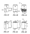
- FIGS. 4A-C provide a schematic representation of an electrical component having capacitor-path inductance cancellation in accordance with the present invention
- FIGS. 4D-F provide a further schematic representation of an electrical component having capacitor-path inductance cancellation in accordance with the present invention
- FIG. 5 is a schematic representation of an exemplary coupled magnetic winding circuit that can form a part of a filter element having inductance cancellation in accordance with the present invention
- FIG. 6 is a schematic representation of another exemplary coupled magnetic winding circuit that can form a part of a filter element having inductance cancellation in accordance with the present invention
- FIG. 7 is a circuit diagram of an exemplary equivalent circuit model for the circuit of FIG. 5 ;
- FIG. 8 is a circuit diagram of an exemplary physically-based circuit model for coupled magnetic windings that can form a part of a electrical component having inductance cancellation in accordance with the present invention
- FIG. 9 is a circuit diagram of the circuit model of FIG. 7 applied to a capacitor
- FIG. 10A is a histogram of Equivalent Series Inductance for an exemplary capacitor
- FIG. 10B is a histogram of Equivalent Series Resistance for an exemplary capacitor
- FIG. 11A is a schematic depiction of coupled windings on a former that can form part of a component having inductance cancellation in accordance with the present invention
- FIG. 11B is a schematic depiction of coupled windings on a former used in conjunction with a capacitor to form a component having capacitor-path inductance cancellation in accordance with the present invention
- FIGS. 12A-C are a pictorial representation of an exemplary implementation of a component having inductance cancellation in accordance with the present invention.
- FIG. 13A is schematic depiction of a component having inductance cancellation in accordance with the present invention and an adaptive inductance cancellation circuit;
- FIG. 13B is a cross-sectional schematic depiction of a cross-field reactor that can form a part of a component having inductance cancellation in accordance with the present invention
- FIG. 13C is a schematic depiction of a component having inductance cancellation and an adaptive inductance cancellation circuit in accordance with the present invention.
- FIG. 14 is a pictorial representation of an integrated component having inductance cancellation in accordance with the present invention.
- FIGS. 15A-C show an integrated filter element having inductance cancellation in accordance with the present invention
- FIG. 16 is a schematic depiction of an exemplary circuit for evaluating a component having inductance cancellation in accordance with the present invention
- FIG. 16A is a graphical representation of power over frequency for a conventional capacitor
- FIG. 16B is a graphical representation of power over frequency for a component having inductance cancellation in accordance with the present invention.
- FIG. 17A is an illustration of a test setup useful for evaluating the attenuation performance of capacitors, components, and filters;
- FIG. 17B is a graphical depiction of power over frequency for a conventional capacitor and a component having inductance cancellation in accordance with the present invention.
- FIG. 17C is a graphical depiction of power over frequency for a conventional capacitor and a component having inductance cancellation in accordance with the present invention.
- FIG. 18 is a schematic depiction of a delta model of the capacitance of an electrode network
- FIG. 19A is a schematic depiction of a prior art model of a filter inductor
- FIG. 19B is a schematic depiction of the connection of a coupled electrode network with an inductor to form a component having capacitance cancellation in accordance with the present invention.
- FIG. 20 is a pictorial representation of a coupled electrode network in accordance with the present invention.
- FIG. 4A shows an electrical component 100 having a capacitor 102 and coupled magnetic windings 104 A,B to cancel the equivalent series inductance of the capacitor and also to provide series filter impedance in the other filter branch.
- a first winding 104 B which can be provided as foil, is wound about the capacitor 102 (FIGS. 4 C and 4 B).
- a second winding 104 A which can be provided as a wire winding, is placed over the first winding 104 B such that the windings are coupled.
- the coupled magnetic windings 104 effectively nullify the inductance of the capacitor 102 and can provide series filter impedance in the other filter path, as described in detail below. It is understood that inductance cancellation refers to cancellation of an inductive characteristic component of capacitors or other components.
- FIG. 4D shows an electrical component 105 having a capacitor 106 and coupled magnetic windings 107 to cancel the equivalent series inductance in the electrical path of the capacitor, and also to provide series impedance in the other electrical path.
- the magnetic windings are formed from a single conductor and insulating layer wound about the capacitor 106 ( FIGS. 4F and 4E ) with the conductor tapped at an appropriate point 109 .
- the coupled magnetic windings 107 formed from the wound and tapped conductor effectively cancel the inductance in the electrical path of the capacitor 106 , and can provide inductive impedance in another electrical path, as described in detail below.
- FIG. 5 shows one exemplary embodiment of a coupled magnetic winding circuit 200 , which can correspond to the coupled magnetic windings 104 of FIG. 4 A.
- the circuit 200 includes inductively coupled first and second windings W 1 , W 2 .
- a first terminal T 1 is coupled to a first end 202 of the first winding W 1 and to a first end 204 of the second winding W 2 .
- a second terminal T 2 is coupled to the second end 206 of the second winding W 2 and a third terminal T 3 is coupled to the second end 208 of the first winding W 1 .
- Current flow is indicated by arrows i 1 , i 2 .
- the first winding W 1 generates a first flux ⁇ 1 and the second winding W 2 generates a second flux ⁇ 2 .
- the first and second windings W 1 ,W 2 are magnetically coupled, and together produce a mutual flux ⁇ M .
- FIG. 6 shows an alternative exemplary embodiment of a three-terminal coupled magnetic winding circuit 200 ′ that can correspond to the coupled magnetic windings 107 of FIG. 4 D.
- the circuit 200 ′ includes magnetically-coupled first and second windings W 1 ′ and W 2 ′, which may optionally be formed from a single winding tapped at an appropriate point.
- a first terminal T 1 is coupled to a first end 212 of the first winding W 1 ′.
- a second terminal T 2 is coupled to a second end 218 of the second winding W 2 ′.
- a third terminal T 3 is coupled to a second end 214 of the first winding W 1 ′ and a first end 216 of the second winding W 2 ′.
- the first winding W 1 ′ generates a first flux ⁇ 1 and the second winding W 2 ′ generates a second flux ⁇ 2 .
- the first and second windings W 1 ′,W 2 ′ are magnetically coupled, and together produce a mutual flux ⁇ M .
- ⁇ 1 where the flux linkages ⁇ 1 and ⁇ 2 are the integrals of the individual coil voltages, i 1 and i 2 are the individual coil currents, N 1 and N 2 represent the number of turns on the respective coils W 1 , W 2 , and , represent the reluctances of the respective magnetic flux paths.
- the self inductances L 11 and L 22 and mutual inductance L M are functions of the numbers of coil turns N 1 , N 2 and the reluctances , of the magnetic flux paths. It is understood that where no magnetic material is present, the behavior of the coupled windings is determined principally by the geometry of the windings.
- FIG. 7 shows an equivalent circuit model 300 for the coupled magnetic winding circuit 200 of FIG. 5 and circuit 200 ′ of FIG. 6 .
- the circuit model 300 can be referred to as a “T-circuit.”
- the circuit model 300 represents a circuit analysis tool and is not intended to provide a physical model of the actual circuit.
- the circuit model 300 includes three inductors L A , L B , and L C . In representing the coupled magnetic winding circuit 200 of FIG.
- inductance L A equals a mutual inductance L M , which represents a mutual inductance of first and second windings W 1 , W 2 ;
- the inductance of the inductor L C corresponds to the self inductance L 11 of the first winding W 1 minus the mutual inductance L M , i.e., L 11 ⁇ L M ;
- the inductance of the inductor L B corresponds to the self inductance L 22 of the second winding W 2 minus the mutual inductance L M , i.e., L 22 ⁇ L M .
- Equation 2 L M ⁇ square root over (L 11 L 22 ) ⁇ Eq. 2
- Equation 3 L 11 ⁇ L M ⁇ square root over (L 11 L 22 ) ⁇ L 22 Eq. 3
- FIG. 9 shows the application of the coupled magnetic windings of FIG. 5 to a capacitor C F whose equivalent series inductance L ESL is to be cancelled or nullified.
- the coupled windings are modeled with the T network 300 of FIG. 7 , while the capacitor C F is shown as an ideal capacitor in series with parasitic resistance R ESR and parasitic inductance L ESL . It is understood that any interconnect parasitics can be lumped into these elements.
- the combined network is advantageous as a filter since a near-zero capacitor-path impedance (limited only by ESR) is maintained out to significantly higher frequencies than is possible with the capacitor alone. Furthermore, when L 22 is much greater than L M , the inductance L 22 ⁇ L M appearing in the other branch serves to increase the order of the filter network, further improving filter performance.
- FIG. 6 another exemplary embodiment of a three-terminal coupled magnetic winding circuit 200 ′ is shown that can be used for inductance cancellation. This embodiment is advantageous in that it can be formed from a single winding tapped at an appropriate point, as suggested by FIGS. 4D-F .
- one branch of the T model has a negative inductance (in this case equal in magnitude to the mutual inductance L M ).
- L M is chosen to be close in magnitude to the equivalent series inductance L ESL of an electrical circuit path (e.g., through a capacitor) connected to terminal T 3
- coupled magnetic windings are used to cancel inductance in the capacitor branch path (e.g., due to capacitor and interconnect parasitics) and provide filter inductance in the other branch path.
- this corresponds to a cancellation of the filter shunt-path inductance, and an addition of series path inductance. It is understood that the inductances to be cancelled can be quite small (e.g., on the order of tens of nanohenries).
- FIGS. 10A and 10B show the distribution of ESL and ESR, respectively, for an electrolytic capacitor identified as United Chemi-Con U767D 2200 ⁇ F 35 V, which is widely used in filters.
- ESL values fall in the range of 17.29 nH to 18.13 nH with a standard deviation of about 44.6 pH.
- the ESR ranges from about 14.2 m ⁇ to about 60.9 m ⁇ (note that worst-case 60 m ⁇ outlier not illustrated in FIG. 10 B). Coupled magnetic windings appropriate to inductance cancellation in accordance with the present invention should accurately generate a negative effective shunt inductance in this range.
- capacitor ESL is typically highly consistent.
- the ESL of all units measured is within ⁇ 2.4% of the mean, with a standard deviation of only 44.6 pH.
- the absence of magnetic materials means that the inductance of the structure depends primarily on geometry, while capacitance and resistance depend on material and interface properties.
- the parasitic inductance can be repeatably cancelled to within a few percent of its original value. This can translate into orders of magnitude improvement in filter attenuation performance.
- a capacitive component having parasitic inductance cancellation in accordance with the present invention can be achieved in a variety of structures.
- discrete capacitors and coupled magnetic windings can be used to create high-performance filters and filter stages.
- magnetic windings can be incorporated on, in, and/or as part of the capacitor structure itself.
- An integrated filter element can be provided as a three terminal device providing both capacitance (with very low effective inductance) in one electrical path and inductance in another electrical path.
- One approach is to construct filters or filter stages in which discrete coupled windings are used to cancel capacitor and interconnect inductance in the capacitive path of the filter.
- the discrete coupled windings realize the effective negative shunt inductance accurately and repeatably.
- Illustrative fabrication techniques include using foil and/or wire windings and using windings printed or metallized on a flexible material.
- Nonmagnetic formers which provide “air-core” magnetics, can be used for the relatively small inductances needed and for repeatability and insensitivity to operating conditions. Magnetic materials can be utilized depending upon the requirements of a particular application.
- FIG. 11 a shows exemplary coupled magnetics 400 , comprising windings 402 A,B wound on a former 401 .
- the former 401 can be mountable on a printed circuit board, for example, though this is not necessary.
- the windings 402 A and 402 B are electrically configured and magnetically coupled as illustrated in FIG. 5 to provide the desired characteristics.
- FIG. 11 b illustrates the coupled magnetics 400 electrically connected to a capacitor 403 to form a filter component. It will be readily apparent to one of ordinary skill in the art that the that the capacitor and coupled magnetics can be physically configured in a wide variety of ways, and that electrical connections can be provided in a number of configurations, including as part of a printed circuit board.
- FIGS. 12A-C the coupled windings are “printed” as part of a filter printed circuit board (PCB).
- FIG. 12A shows first and second capacitors 450 a , 450 b mounted on a two-sided printed circuit board 451 with printed windings that realize inductance cancellation for each capacitor.
- the first capacitor 450 a is connected to a pair of rectangular coupled windings 452 a , 453 a that are printed in the circuit board underneath the capacitor 450 a .
- the second capacitor 450 b is similarly connected to a pair of circular (spiral) coupled windings 452 b , 453 b .
- the pairs of coupled magnetic windings are each configured as illustrated in FIG. 5 to realize inductance cancellation.
- FIG. 12B shows the top (component) side of printed circuit board 451 without the capacitors mounted so that the top side windings 452 a , 452 b (each corresponding to coil W 1 in FIG. 5 ) can be seen.
- FIG. 12C shows the bottom side of printed circuit board 451 so that the bottom side windings 453 a , 453 b (each corresponding to coil W 2 in FIG. 5 ) can be seen.
- printing the magnetic windings on the PCB results in repeatable magnetic structures and interconnects. Again, an air-core structure is advantageous, though magnetic materials may be used.
- a filter circuit 500 having inductance cancellation can include magnetic materials in the cancellation windings and an adaptive inductance cancellation feature.
- adaptive inductance cancellation can be applicable for components having cancellation windings integrated into part of another filter or power converter component.
- the circuit 500 includes a capacitor C coupled to a cross-field magnetic structure 502 , which includes a toroidal control coil 504 and coupled annular coils 506 a and 506 b wound on a magnetic core 508 , as shown in FIG. 13B.
- a feedback circuit 510 adjusts the current in the toroidal coil 504 to optimize the inductance cancellation provided by the annular coils 506 a , 506 b .
- the magnetic field generated by the winding 504 does not substantially link the windings 506 a and 506 b and vice versa, so there is no “transformer” action between the annular winding and the two toroidal windings.
- the coupled annular windings 506 a and 506 b can be referred to as the cancellation windings, which serve to realize the inductance cancellation technique.
- the toroidal winding 504 which can be referred to as the control winding, carries a low frequency control current that modulates the effective permeability of the magnetic material by driving it a controlled amount into saturation.
- the control winding 504 can thus control the effective magnetic coupling seen by the cancellation windings 506 a and 506 b .
- the magnetic coupling can be adaptively controlled to maximize filter performance.
- FIG. 13C illustrates a further illustrative embodiment having adaptive inductance cancellation.
- a filter circuit 550 includes coupled magnetics 551 , a cross-field reactor 552 , a feedback control circuit 553 , and a capacitor 554 .
- coupled magnetics 551 implement the coupled windings for inductance cancellation (and for inductance in the other filter path), and may have other functions as well, depending on the application. Such other functions may include, for example, acting as power stage or filter magnetics in a power converter, or providing electrical isolation.
- the cross-field reactor 552 has an annular winding 555 in the electrical path between the coupled magnetics 550 and the capacitor 554 .
- the annular winding 555 provides inductance in the capacitor path of the filter, which is electrically adjustable from a toroidal control winding 556 .
- the total capacitor path inductance can be adaptively controlled to maximize filter performance.
- the adaptive inductance cancellation feature of FIGS. 13A and 13C includes the coupling of the magnetic circuit under closed-loop control with feedback based on the characteristics of the filter waveforms. For example, techniques such as ripple correlation control may be employed to adapt for maximum filter performance.
- This adaptive inductance cancellation approach can achieve high filter performance while providing a high tolerance to manufacturing and environmental variations in both the magnetic elements and the shunt capacitor.
- coupled magnetic windings are combined with a capacitor to form an integrated filter element having inductance cancellation in accordance with the present invention.
- the integrated element can be provided as a single three-terminal device having a T model with one low-inductance branch, one capacitive branch (with extremely low inductance) and one high-inductance branch.
- the integrated element can be provided as a single three-terminal device having a T model with two moderately inductive branches, and a capacitive branch with extremely low inductance.
- the coupled magnetics can be wound on, within, or as part of the capacitor.
- FIG. 14 shows an exemplary component 600 having a capacitor 602 integrated with coupled first and second windings 604 a,b .
- the component 600 includes a wound (tubular) capacitor 602 with coupled magnetics 604 a,b wound directly on top of the capacitor winding.
- the other end of the magnetic winding 604 b is brought out as a terminal 604 c .
- One side of the capacitor plate structure is connected internally to the internal end of winding 604 a , and the other side of the capacitor plate structure is brought out externally as terminal 604 d .
- the magnetic windings can be made by extending the patterning of the capacitor foil or metallization. This arrangement minimizes the volume of the overall structure since the same volume is used for the capacitive and magnetic energy storage.
- FIGS. 15A-C show various fabrication stages of an illustrative prototype filter element 700 having inductance cancellation in accordance with the present invention.
- Inductance cancellation magnetics 702 a,b were wound on the outside of a United Chemi-Con U767D 2200 ⁇ F, 35 V electrolytic capacitor 704 .
- a first (capacitor-path) winding 702 a which is shown as a foil winding, is added about the capacitor package.
- a second (inductive-path) winding 702 b which is shown as a wire winding, is placed over the first winding 702 a .
- Use of the capacitor body as the winding form minimizes the overall volume of the filter element and illustrates the possibility of incorporating the coupled windings inside the capacitor package.
- the capacitor-path winding 702 a is wound with 1 inch wide, 1 mil thick copper tape, insulated with 1 mil mylar tape. One and three fourths turns on the capacitor body (circumference of 7.1 cm) were found to be sufficient to achieve a desired level of coupling.
- the inductive-path winding 702 b is composed of several turns of 18 gauge magnet wire coiled tightly over the ac winding and glued in place. The two windings are soldered together at one end (forming one terminal), and the other end of the capacitor-path winding is soldered to the positive terminal of the capacitor.
- the prototype demonstrates significant performance improvement over known capacitors.
- the three-terminal filter element is only marginally larger than the original capacitor.
- the action of the coupled windings was found to cancel the effective capacitor-path inductance down to approximately 15-25% of its original value, while providing over 700 nH of series-path filter inductance.
- EMI Electromagnetic Interference
- a device under test DUT i.e., the integrated filter 700 of FIG. 15C and a conventional capacitor, were used as the principle low-pass filter element at the input of a buck converter 750 .
- small high-frequency capacitors C 1 , C 2 were added in parallel with the device under test DUT.
- Attenuation performance was evaluated using conventional EMI measurement techniques.
- Ripple was evaluated at the measurement port of a Line Impedance Stabilization Network (LISN) 752 in A-B comparisons between a capacitor and the prototype filter element.
- LISN Line Impedance Stabilization Network
- the attenuation of the prototype filter element 700 exceeds that of the capacitor alone by over 25 dB (a factor of 17) across the entire measured spectrum (100 kHz-2 MHz). This represents a significant improvement in filtration capability without a significant increase in component volume. Furthermore, further performance improvements are expected when the invention is refined over the prototype.
- FIG. 17A illustrates a measurement system suitable for evaluating the attenuation performance of capacitors, filter components, and filters.
- a drive signal is injected from the 50 Ohm output of a network analyzer 832 a into the device under test (DUT) (i.e. a capacitor and a capacitor plus cancellation windings), and the resulting filter output is measured at the 50 Ohm network analyzer input 832 b via the line impedance stabilization network (LISN) 834 .
- the response thus measures the ability of the DUT to attenuate an input signal.
- FIG. 17B shows the performance of a capacitor alone 800 and a component 802 having inductance cancellation in accordance with the present invention, such as the device shown in FIG. 12A implemented with Cornell Dubilier 935C4W10K capacitors (10 ⁇ F, 400 V).
- a first curve 800 shows the signal power measured with the capacitor alone. The minimum of the curve (between 100 and 200 kHz) illustrates where the filter capacitor reaches its self resonance; at higher frequencies it appears inductive and does not attenuate the input as well.
- a second curve 802 shows the performance with the cancellation windings. As can be seen, the attenuation remains high out to significantly higher frequencies, and performs at least a factor of 10 (20 dB) better for all frequencies above about 600 kHz.
- FIG. 17C a third example serves to demonstrate the present invention with the coupled winding configuration of FIG. 6.
- a prototype filter element was constructed in a manner similar to the fashion illustrated in FIGS. 4D-F .
- a Cornell-Dubilier 935C4W10K capacitor (10 ⁇ F, 400 V) having a diameter of 1.5 inches was wound with 2 turns of 1 mil thick 550 mil wide copper foil insulated on one side with 1 mil thick mylar tape. The winding was tapped at the 2-turn point and connected to one terminal of the capacitor. The winding was then continued for an additional 1.5 turns. The end point of the winding was selected to provide good inductance cancellation based on the ability of the circuit to attenuate an input signal.
- FIG. 17C shows the measured performance of the prototype device and a capacitor alone using the test setup of FIG. 17A.
- a first curve 840 (in FIG. 17C ) shows the signal power measured with the capacitor alone. The minimum of the curve 840 illustrates where the filter capacitor reaches its self resonance; at higher frequencies it appears inductive and does not attenuate the input as well.
- a second curve 842 shows the performance with the cancellation windings. With the cancellation windings the attenuation is substantially better (>20 dB) at high frequencies.
- a resonant peaking appears around 1.4 MHz, where the secondary resonance peculiar to this capacitor occurs (and where its effective ESL changes slightly).
- the parasitic capacitance of magnetic elements can be effectively cancelled through proper capacitive coupling of a network of electrodes. It is understood that conservation of energy laws prohibit passive realization of a two-terminal negative capacitance. However, a multi-electrode network may exhibit an apparent negative capacitance in a single branch of a delta network model, which is shown in FIG. 18 , as long as certain physical constraints are met.
- a multi-electrode network may exhibit an apparent negative capacitance in a single branch of a delta network model, which is shown in FIG. 18 , as long as certain physical constraints are met.
- One of ordinary skill in the art will recognize that such an arrangement is the dual of the coupled magnetic embodiments described above. Proper application of such coupled electrodes may be effective in addressing the high-frequency limitations of inductors, thereby further improving achievable filter performance.
- FIG. 19A shows a prior-art model for a conventional filter inductor L, including parasitic resistances R P1 and R P2 , and parasitic capacitance C P .
- the parasitic capacitance arises from interwinding capacitance of the inductor and other effects. It is of particular significance in filter applications because it limits the component's ability to attenuate voltage ripple at high frequencies: the magnitude of the impedance falls off above the self resonance of the inductance and the parasitic capacitance.
- interconnection of the inductor L which can be modeled using the model 900 of FIG. 19A , with an electrode network 902 having an appropriate characteristic (e.g. having a delta model in which one branch of the delta appears as a negative capacitance) provides a component 904 with improved performance.
- the component 904 has relatively low effective capacitance across the nodes to which the inductor is connected (due to capacitance cancellation), and provides additional filter capacitance from each of those nodes to the third node.
- An exemplary structure having a plurality of electrodes ELa-d is illustrated in FIG. 20 .
- the present invention provides a novel filtering technique that overcomes the high-frequency limitations of known filter capacitors. Coupled magnetic windings are used to cancel filter capacitor-path inductance (e.g., due to capacitor and interconnect parasitics) and provide filter inductance in another filter path. This arrangement is advantageous since the amount of attenuation provided by a filter stage depends directly on the mismatch between the impedances of the two paths.
- the invention is useful in the design of filters and in the design of integrated filter elements.
- discrete coupled windings are used to cancel capacitor and interconnect inductance in the filter capacitive path.
- the coupled windings may be wound or printed, and may also incorporate adaptive control of the inductance cancellation.
- the magnetic windings are incorporated with the capacitor to form an integrated filter component.
- the integrated element utilizes the inventive inductance cancellation technique to realize both a capacitive path having extremely low effective ESL and an inductive path.
Abstract
Description
where the flux linkages λ1 and λ2 are the integrals of the individual coil voltages, i1 and i2 are the individual coil currents, N1 and N2 represent the number of turns on the respective coils W1, W2, and
L M ≦√{square root over (L 11 L 22 )} Eq. 2
Thus, the inductance matrix of
L 11 <L M <√{square root over (L 11 L 22 )}< L 22 Eq. 3
where the flux linkages λ1 and λ2 are the integrals of the individual coil voltages, i1 and i2 are the individual coil currents, N1 and N2 represent the number of turns on the respective coils W1′, W2′, and
Claims (43)
Priority Applications (4)
| Application Number | Priority Date | Filing Date | Title |
|---|---|---|---|
| US10/082,616 US6937115B2 (en) | 2002-02-25 | 2002-02-25 | Filter having parasitic inductance cancellation |
| PCT/US2002/037961 WO2003073608A1 (en) | 2002-02-25 | 2002-11-27 | Filter having parasitic inductance cancellation |
| AU2002348253A AU2002348253A1 (en) | 2002-02-25 | 2002-11-27 | Filter having parasitic inductance cancellation |
| US11/119,659 US7242269B2 (en) | 2002-02-25 | 2005-05-02 | Filter having parasitic inductance cancellation |
Applications Claiming Priority (1)
| Application Number | Priority Date | Filing Date | Title |
|---|---|---|---|
| US10/082,616 US6937115B2 (en) | 2002-02-25 | 2002-02-25 | Filter having parasitic inductance cancellation |
Related Child Applications (1)
| Application Number | Title | Priority Date | Filing Date |
|---|---|---|---|
| US11/119,659 Continuation-In-Part US7242269B2 (en) | 2002-02-25 | 2005-05-02 | Filter having parasitic inductance cancellation |
Publications (2)
| Publication Number | Publication Date |
|---|---|
| US20030210110A1 US20030210110A1 (en) | 2003-11-13 |
| US6937115B2 true US6937115B2 (en) | 2005-08-30 |
Family
ID=27765283
Family Applications (2)
| Application Number | Title | Priority Date | Filing Date |
|---|---|---|---|
| US10/082,616 Expired - Lifetime US6937115B2 (en) | 2002-02-25 | 2002-02-25 | Filter having parasitic inductance cancellation |
| US11/119,659 Expired - Fee Related US7242269B2 (en) | 2002-02-25 | 2005-05-02 | Filter having parasitic inductance cancellation |
Family Applications After (1)
| Application Number | Title | Priority Date | Filing Date |
|---|---|---|---|
| US11/119,659 Expired - Fee Related US7242269B2 (en) | 2002-02-25 | 2005-05-02 | Filter having parasitic inductance cancellation |
Country Status (3)
| Country | Link |
|---|---|
| US (2) | US6937115B2 (en) |
| AU (1) | AU2002348253A1 (en) |
| WO (1) | WO2003073608A1 (en) |
Cited By (14)
| Publication number | Priority date | Publication date | Assignee | Title |
|---|---|---|---|---|
| US20060114634A1 (en) * | 2004-11-30 | 2006-06-01 | Tdk Corporation | Surge absorption circuit |
| US20070025043A1 (en) * | 2005-07-29 | 2007-02-01 | Tdk Corporation | Surge absorption element and surge absorption circuit |
| US20070076343A1 (en) * | 2005-09-30 | 2007-04-05 | Tdk Corporation | Connector |
| US20070233408A1 (en) * | 2006-03-31 | 2007-10-04 | Hon Hai Precision Industry Co., Ltd. | System and method for calculating a voltage spike value |
| US20080228415A1 (en) * | 2002-10-11 | 2008-09-18 | Peter Ladbrooke | Semiconductor testing instrument to determine safe operating area |
| US20090096068A1 (en) * | 2007-10-12 | 2009-04-16 | Johan Sjoestroem | System and Method for Stabilizing an Amplifier |
| US20100283438A1 (en) * | 2009-05-05 | 2010-11-11 | City University Of Hong Kong | Output compensator for a regulator |
| US20100283437A1 (en) * | 2009-05-05 | 2010-11-11 | City University Of Hong Kong | Method and apparatus for suppressing noise caused by parasitic inductance and/or resistance in an electronic circuit or system |
| US20100283436A1 (en) * | 2009-05-05 | 2010-11-11 | City University Of Hong Kong | Method and apparatus for suppressing noise caused by parasitic capacitance and/or resistance in an electronic circuit or system |
| US20150214611A1 (en) * | 2010-01-19 | 2015-07-30 | Murata Manufacturing Co., Ltd. | Antenna device and communication terminal apparatus |
| US9825522B2 (en) | 2015-04-09 | 2017-11-21 | Ford Global Technologies, Llc | Method and apparatus for coupling cancellation |
| US20180083539A1 (en) * | 2016-09-21 | 2018-03-22 | Express Imaging Systems, Llc | Output ripple reduction for power converters |
| WO2020017368A1 (en) | 2018-07-17 | 2020-01-23 | 株式会社豊田中央研究所 | Noise filter |
| US10790784B2 (en) | 2014-12-19 | 2020-09-29 | Massachusetts Institute Of Technology | Generation and synchronization of pulse-width modulated (PWM) waveforms for radio-frequency (RF) applications |
Families Citing this family (15)
| Publication number | Priority date | Publication date | Assignee | Title |
|---|---|---|---|---|
| US7228119B2 (en) * | 2002-12-30 | 2007-06-05 | Motorola, Inc. | Apparatus and method for a radio frequency (RF) receiver front end pre-selector tuning for improving the reduction in intermodulation distortion (IMD) |
| US7180389B2 (en) | 2004-12-17 | 2007-02-20 | Virginia Tech Intellectual Properties, Inc. | EMI filter and frequency filters having capacitor with inductance cancellation loop |
| US20090040001A1 (en) * | 2005-10-10 | 2009-02-12 | George Young | Power converter |
| US7589605B2 (en) * | 2006-02-15 | 2009-09-15 | Massachusetts Institute Of Technology | Method and apparatus to provide compensation for parasitic inductance of multiple capacitors |
| US7535125B2 (en) * | 2006-05-09 | 2009-05-19 | Mte Corporation | Single-phase filter for reducing harmonics |
| TWI449066B (en) * | 2010-01-19 | 2014-08-11 | Murata Manufacturing Co | High coupling degree transformers, electronic circuits and electronic machines |
| US8242626B1 (en) * | 2010-05-17 | 2012-08-14 | The United States Of America As Represented By The Secretary Of The Navy | Magneto-electric method and apparatus for remote powering on the hull of an underwater vehicle |
| WO2012114983A1 (en) * | 2011-02-23 | 2012-08-30 | 株式会社村田製作所 | Impedance conversion circuit and transmission terminal apparatus |
| DE102011007833A1 (en) * | 2011-04-21 | 2012-10-25 | Robert Bosch Gmbh | Extinguishing parasitic inductances in filter capacitors connected in parallel to electrical converters in a vehicle electrical system for a vehicle |
| WO2013044918A2 (en) * | 2011-09-30 | 2013-04-04 | Vestas Wind Systems A/S | A harmonic filter arrangement |
| US20160182001A1 (en) * | 2014-12-19 | 2016-06-23 | Hitachi, Ltd | Common mode noise filter |
| US20160285360A1 (en) * | 2015-03-24 | 2016-09-29 | Ford Global Technologies, Llc | Method and apparatus for electromagnetic interference reduction |
| JP6472344B2 (en) * | 2015-06-30 | 2019-02-20 | 三菱電機株式会社 | Noise filter and printed circuit board |
| US10862521B1 (en) * | 2019-01-30 | 2020-12-08 | Inphi Corporation | Techniques for programmable gain attenuation in wideband matching networks with enhanced bandwidth |
| CN113795898A (en) | 2019-03-27 | 2021-12-14 | 恩纽尔有限公司 | Multiphase switching regulator |
Citations (15)
| Publication number | Priority date | Publication date | Assignee | Title |
|---|---|---|---|---|
| US1920948A (en) | 1928-01-27 | 1933-08-01 | Byrnes Townsend & Potter | Electrical filter |
| US3465267A (en) | 1966-03-04 | 1969-09-02 | Ernest H Carlson Jr | Circuit component |
| US4422059A (en) * | 1981-04-08 | 1983-12-20 | Matsushita Electric Industrial Co., Ltd. | Band-pass filter having multilayered coil structures |
| US4451804A (en) * | 1981-09-01 | 1984-05-29 | Veisz Gyoergy | Four-terminal network |
| US4577145A (en) * | 1984-10-11 | 1986-03-18 | General Electric Company | Charging system having electromagnetic field means for distinguishing between primary and secondary batteries |
| US5038263A (en) | 1990-01-03 | 1991-08-06 | Eg&G Power Systems, Inc. | Ripple current reduction circuit |
| US5148360A (en) * | 1992-01-29 | 1992-09-15 | Gte Products Corporation | Fourth order damped lowpass filter for obtaining high power factor and low total harmonic distortion |
| JPH06224045A (en) | 1993-01-28 | 1994-08-12 | Soshin Denki Kk | Lc composite element |
| US5495405A (en) * | 1993-08-30 | 1996-02-27 | Masakazu Ushijima | Inverter circuit for use with discharge tube |
| US5694297A (en) * | 1995-09-05 | 1997-12-02 | Astec International Limited | Integrated circuit mounting structure including a switching power supply |
| US5761049A (en) | 1994-09-19 | 1998-06-02 | Hitachi, Ltd. | Inductance cancelled condenser implemented apparatus |
| US6239557B1 (en) * | 2000-03-14 | 2001-05-29 | Philips Electronics North America Corporation | Transformer winding technique with reduced parasitic capacitance effects |
| JP2001160728A (en) | 1999-09-21 | 2001-06-12 | Murata Mfg Co Ltd | Lc filter |
| US6476689B1 (en) | 1999-09-21 | 2002-11-05 | Murata Manufacturing Co., Ltd. | LC filter with capacitor electrode plate not interfering with flux of two coils |
| US6529363B2 (en) * | 2000-06-21 | 2003-03-04 | Koninklijke Philips Electronics N.V. | Capacitor integrated into transformer by multi-layer foil winding |
Family Cites Families (2)
| Publication number | Priority date | Publication date | Assignee | Title |
|---|---|---|---|---|
| US1920947A (en) * | 1930-07-25 | 1933-08-01 | Jeffrey Mfg Co | Rotary material reducing machine |
| US5148804A (en) | 1990-06-28 | 1992-09-22 | Hill Dennis M | Device, system, and methods for applying cryotherapy |
-
2002
- 2002-02-25 US US10/082,616 patent/US6937115B2/en not_active Expired - Lifetime
- 2002-11-27 AU AU2002348253A patent/AU2002348253A1/en not_active Abandoned
- 2002-11-27 WO PCT/US2002/037961 patent/WO2003073608A1/en not_active Application Discontinuation
-
2005
- 2005-05-02 US US11/119,659 patent/US7242269B2/en not_active Expired - Fee Related
Patent Citations (15)
| Publication number | Priority date | Publication date | Assignee | Title |
|---|---|---|---|---|
| US1920948A (en) | 1928-01-27 | 1933-08-01 | Byrnes Townsend & Potter | Electrical filter |
| US3465267A (en) | 1966-03-04 | 1969-09-02 | Ernest H Carlson Jr | Circuit component |
| US4422059A (en) * | 1981-04-08 | 1983-12-20 | Matsushita Electric Industrial Co., Ltd. | Band-pass filter having multilayered coil structures |
| US4451804A (en) * | 1981-09-01 | 1984-05-29 | Veisz Gyoergy | Four-terminal network |
| US4577145A (en) * | 1984-10-11 | 1986-03-18 | General Electric Company | Charging system having electromagnetic field means for distinguishing between primary and secondary batteries |
| US5038263A (en) | 1990-01-03 | 1991-08-06 | Eg&G Power Systems, Inc. | Ripple current reduction circuit |
| US5148360A (en) * | 1992-01-29 | 1992-09-15 | Gte Products Corporation | Fourth order damped lowpass filter for obtaining high power factor and low total harmonic distortion |
| JPH06224045A (en) | 1993-01-28 | 1994-08-12 | Soshin Denki Kk | Lc composite element |
| US5495405A (en) * | 1993-08-30 | 1996-02-27 | Masakazu Ushijima | Inverter circuit for use with discharge tube |
| US5761049A (en) | 1994-09-19 | 1998-06-02 | Hitachi, Ltd. | Inductance cancelled condenser implemented apparatus |
| US5694297A (en) * | 1995-09-05 | 1997-12-02 | Astec International Limited | Integrated circuit mounting structure including a switching power supply |
| JP2001160728A (en) | 1999-09-21 | 2001-06-12 | Murata Mfg Co Ltd | Lc filter |
| US6476689B1 (en) | 1999-09-21 | 2002-11-05 | Murata Manufacturing Co., Ltd. | LC filter with capacitor electrode plate not interfering with flux of two coils |
| US6239557B1 (en) * | 2000-03-14 | 2001-05-29 | Philips Electronics North America Corporation | Transformer winding technique with reduced parasitic capacitance effects |
| US6529363B2 (en) * | 2000-06-21 | 2003-03-04 | Koninklijke Philips Electronics N.V. | Capacitor integrated into transformer by multi-layer foil winding |
Non-Patent Citations (12)
| Title |
|---|
| D.L. Logue and P.T. Krein, Optimization of Power Electronic Systems Using Ripple Correlation Control: A Dynamioc Programming Approach, 2001 IEEE Power Electronics Specialists Conference, pp. 459-464. |
| David C. Hamill, Philip T. Krein, A Zero Ripple Technique Applicable To Any DC Converter, , 1999 IEEE Power Electronics Specialists Conference, pp. 1165-1171. |
| H. J. McCreary, The Magnetic Cross Valve, AIEE Transactions, vol. 70, Pt. II, pp. 1868-1875. |
| Johann W. Kolar, Hari Sree, Ned Mohan, Franz C. Zach, Novel Aspects of an Application of 'Zero '-Ripple Techniques to Basic Converter Topologies, 1997 IEEE Power Electronics Specialists Conference, pp. 796-803. |
| Joshua W. Phinney, Filters with Active Tuning for Power Applications, May 30, 2002, pp. 1-133. |
| PCT International Search Report PCT/US 02/37961, Filed on Nov. 27, 2002. |
| Powering the Future: New Opportunities in Power Electronics, MIT Laboratory for Electromagnetic and Electronic Systems, Apr. 10, 2001, pp. 1-42. |
| Robert A. Heartz, Herbert Buelteman, Jr., The Application of Perpendicularly Superposed Magnetic Fields, AIEE Trans. Pt. 1, Nov. 1955, vol. 74, pp. 655-660. |
| Sam Y. M. Feng, William A. Sander, III and Thomas G. Wilson, Small-Capacitance Nondissipative Ripple Filters for DC Supplies, IEEE Transactions on Magnetics, Mar. 1970, pp. 137-142. |
| Slobodan CUK, A New Sero-Ripple Switching DC-to-DC Converter and Integrated Magnetics, IEEE Transactions on Magnetics on Magnetics, vol. MAG-19, No. 2, Mar. 1983, pp. 57-75. |
| Steven Senini, Peter J. Wolfs, The Coupled Inductor Filter: Analysis and Design for AC Systems, IEEE Transactions on Idustrial Electronics, vol. 45, No. 4, Aug. 1998, pp. 574-578. |
| T.K. Phelps and W.S. Tate, Optimizing Passive Input Filter Design, Process of the 6<SUP>th </SUP>National Solid State Power Conversion Conference Powercon 6), May 1979, pp. G1-1-G1-10. |
Cited By (29)
| Publication number | Priority date | Publication date | Assignee | Title |
|---|---|---|---|---|
| US20080228415A1 (en) * | 2002-10-11 | 2008-09-18 | Peter Ladbrooke | Semiconductor testing instrument to determine safe operating area |
| US20080192401A1 (en) * | 2004-11-30 | 2008-08-14 | Tdk Corporation | Surge absorption circuit |
| US7821759B2 (en) | 2004-11-30 | 2010-10-26 | Tdk Corporation | Surge absorption circuit |
| US20060114634A1 (en) * | 2004-11-30 | 2006-06-01 | Tdk Corporation | Surge absorption circuit |
| US7397646B2 (en) | 2004-11-30 | 2008-07-08 | Tdk Corporation | Surge absorption circuit |
| US7576965B2 (en) | 2005-07-29 | 2009-08-18 | Tdk Corporation | Surge absorption element and surge absorption circuit |
| US20070025043A1 (en) * | 2005-07-29 | 2007-02-01 | Tdk Corporation | Surge absorption element and surge absorption circuit |
| US7446992B2 (en) * | 2005-09-30 | 2008-11-04 | Tdk Corporation | Connector |
| US20070076343A1 (en) * | 2005-09-30 | 2007-04-05 | Tdk Corporation | Connector |
| US20070233408A1 (en) * | 2006-03-31 | 2007-10-04 | Hon Hai Precision Industry Co., Ltd. | System and method for calculating a voltage spike value |
| US7596460B2 (en) | 2006-03-31 | 2009-09-29 | Hon Hai Precision Industry Co., Ltd. | System and method for calculating a voltage spike value |
| US20090096068A1 (en) * | 2007-10-12 | 2009-04-16 | Johan Sjoestroem | System and Method for Stabilizing an Amplifier |
| US8110932B2 (en) | 2007-10-12 | 2012-02-07 | Infineon Technologies Ag | Semiconductor circuit with amplifier, bond wires and inductance compensating bond wire |
| US20100283436A1 (en) * | 2009-05-05 | 2010-11-11 | City University Of Hong Kong | Method and apparatus for suppressing noise caused by parasitic capacitance and/or resistance in an electronic circuit or system |
| US20100283437A1 (en) * | 2009-05-05 | 2010-11-11 | City University Of Hong Kong | Method and apparatus for suppressing noise caused by parasitic inductance and/or resistance in an electronic circuit or system |
| US20100283438A1 (en) * | 2009-05-05 | 2010-11-11 | City University Of Hong Kong | Output compensator for a regulator |
| US8115537B2 (en) | 2009-05-05 | 2012-02-14 | City University Of Hong Kong | Method and apparatus for suppressing noise caused by parasitic capacitance and/or resistance in an electronic circuit or system |
| US8169201B2 (en) | 2009-05-05 | 2012-05-01 | City University Of Hong Kong | Output compensator for a regulator |
| US8264270B2 (en) | 2009-05-05 | 2012-09-11 | City University Of Hong Kong | Method and apparatus to provide active cancellation of the effects of the parasitic elements in capacitors |
| US9711848B2 (en) * | 2010-01-19 | 2017-07-18 | Murata Manufacturing Co., Ltd. | Antenna device and communication terminal apparatus |
| US20150214611A1 (en) * | 2010-01-19 | 2015-07-30 | Murata Manufacturing Co., Ltd. | Antenna device and communication terminal apparatus |
| US10790784B2 (en) | 2014-12-19 | 2020-09-29 | Massachusetts Institute Of Technology | Generation and synchronization of pulse-width modulated (PWM) waveforms for radio-frequency (RF) applications |
| US11316477B2 (en) | 2014-12-19 | 2022-04-26 | Massachusetts Institute Of Technology | Generation and synchronization of pulse-width modulated (PWM) waveforms for radio-frequency (RF) applications |
| US11942898B2 (en) | 2014-12-19 | 2024-03-26 | Massachusetts Institute Of Technology | Generation and synchronization of pulse-width modulated (PWM) waveforms for radio-frequency (RF) applications |
| US9825522B2 (en) | 2015-04-09 | 2017-11-21 | Ford Global Technologies, Llc | Method and apparatus for coupling cancellation |
| US20180083539A1 (en) * | 2016-09-21 | 2018-03-22 | Express Imaging Systems, Llc | Output ripple reduction for power converters |
| US10230296B2 (en) * | 2016-09-21 | 2019-03-12 | Express Imaging Systems, Llc | Output ripple reduction for power converters |
| WO2020017368A1 (en) | 2018-07-17 | 2020-01-23 | 株式会社豊田中央研究所 | Noise filter |
| US11309859B2 (en) | 2018-07-17 | 2022-04-19 | Kabushiki Kaisha Toyota Chuo Kenkyusho | Noise filter |
Also Published As
| Publication number | Publication date |
|---|---|
| US20060077018A1 (en) | 2006-04-13 |
| US20030210110A1 (en) | 2003-11-13 |
| US7242269B2 (en) | 2007-07-10 |
| WO2003073608A1 (en) | 2003-09-04 |
| AU2002348253A1 (en) | 2003-09-09 |
Similar Documents
| Publication | Publication Date | Title |
|---|---|---|
| US6937115B2 (en) | Filter having parasitic inductance cancellation | |
| US7432793B2 (en) | Amplifier output filter having planar inductor | |
| Neugebauer et al. | Filters and components with inductance cancellation | |
| KR100673347B1 (en) | Noise canceling circuit | |
| US5495213A (en) | LC noise filter | |
| US7548137B2 (en) | Generalized cancellation of inductor winding capacitance | |
| US7199692B2 (en) | Noise suppressor | |
| US20080094153A1 (en) | Cancellation of Inductor Winding Capacitance | |
| KR0145183B1 (en) | Lc noise filter | |
| JP2006100465A (en) | Coil and filter circuit using it | |
| JP3280019B2 (en) | LC noise filter | |
| Neugebauer et al. | Filters and components with inductance cancellation | |
| JP2006287577A (en) | Noise suppressing circuit | |
| JPH0786863A (en) | Noise eliminating parts | |
| CN110945784B (en) | Inductor-capacitor filter and associated systems and methods | |
| JP2006186620A (en) | Line filter | |
| Kuisma et al. | Air-cored common mode filter with integrated capacitors | |
| JP3142060B2 (en) | Noise filter | |
| JP2001211048A (en) | Lc noise filter | |
| JPH0720895Y2 (en) | Inductance element | |
| CN111614094A (en) | Electromagnetic interference filter circuit | |
| JPH0832394A (en) | Noise filter | |
| Gong et al. | Three-dimensional parasitics cancellation in EMI filters with Power Sandwich construction | |
| JP7425727B2 (en) | LC filter arrangements and electrical or electronic devices comprising such LC filter arrangements | |
| WO2023032732A1 (en) | Switching power supply device |
Legal Events
| Date | Code | Title | Description |
|---|---|---|---|
| AS | Assignment |
Owner name: MASSACHUSETTS INSTITUTE OF TECHNOLOGY, MASSACHUSET Free format text: ASSIGNMENT OF ASSIGNORS INTEREST;ASSIGNORS:PERREAULT, DAVID J.;PHINNEY, JOSHUA W.;NEUGEBAUER, TIMOTHY C.;REEL/FRAME:012634/0671 Effective date: 20020221 |
|
| STCF | Information on status: patent grant |
Free format text: PATENTED CASE |
|
| CC | Certificate of correction | ||
| AS | Assignment |
Owner name: NAVY, SECRETARY OF THE, UNITED STATES OF AMERICA O Free format text: CONFIRMATORY LICENSE;ASSIGNOR:MASSACHUSETTS INSTITUTE OF TECHNOLOGY;REEL/FRAME:018249/0259 Effective date: 20050921 |
|
| FPAY | Fee payment |
Year of fee payment: 4 |
|
| FEPP | Fee payment procedure |
Free format text: PAYOR NUMBER ASSIGNED (ORIGINAL EVENT CODE: ASPN); ENTITY STATUS OF PATENT OWNER: LARGE ENTITY |
|
| FEPP | Fee payment procedure |
Free format text: PAT HOLDER NO LONGER CLAIMS SMALL ENTITY STATUS, ENTITY STATUS SET TO UNDISCOUNTED (ORIGINAL EVENT CODE: STOL); ENTITY STATUS OF PATENT OWNER: LARGE ENTITY |
|
| FPAY | Fee payment |
Year of fee payment: 8 |
|
| FPAY | Fee payment |
Year of fee payment: 12 |