US6933752B2 - Method and apparatus for interface signaling using single-ended and differential data signals - Google Patents
Method and apparatus for interface signaling using single-ended and differential data signals Download PDFInfo
- Publication number
- US6933752B2 US6933752B2 US09/870,623 US87062301A US6933752B2 US 6933752 B2 US6933752 B2 US 6933752B2 US 87062301 A US87062301 A US 87062301A US 6933752 B2 US6933752 B2 US 6933752B2
- Authority
- US
- United States
- Prior art keywords
- input
- differential
- data signal
- output
- coupled
- Prior art date
- Legal status (The legal status is an assumption and is not a legal conclusion. Google has not performed a legal analysis and makes no representation as to the accuracy of the status listed.)
- Expired - Lifetime, expires
Links
Images


Classifications
-
- H—ELECTRICITY
- H03—ELECTRONIC CIRCUITRY
- H03K—PULSE TECHNIQUE
- H03K19/00—Logic circuits, i.e. having at least two inputs acting on one output; Inverting circuits
- H03K19/0175—Coupling arrangements; Interface arrangements
- H03K19/0185—Coupling arrangements; Interface arrangements using field effect transistors only
- H03K19/018507—Interface arrangements
- H03K19/018514—Interface arrangements with at least one differential stage
Definitions
- the present invention relates generally to interface signaling, and more particularly, to an interface using both differential and single-ended signals.
- Interfaces between present-day integrated circuits have increased in operating frequency and width.
- microprocessor systems components require both wide and fast connection.
- Data width directly affects the speed of data transmission between systems components, as does the data rate, which is limited by the maximum frequency that can be supported by an interface.
- a differential signaling scheme provides a significant improvement over single-ended signaling, as a differential interface is far less susceptible to common mode noise, produces a more uniform load on the interface power supplies and has a reduced bit error rate (BER).
- BER bit error rate
- an exclusively differential interface requires twice the number of interconnects and associated drivers, as well as a differential receiver for each data signal. Due to the large data widths required in present-day systems, it is not practical to implement a completely differential interface. Interfaces have been developed to improve the detection of single-ended signals, but these require transmission of separate clock signals or other reference signals that provide improved performance, but require interconnects for the reference signals. Additionally, the fan-out requirements of the reference signals complicate the scalability of the designs. When interface width is increased, the number of receivers is also increased, increasing the load on the reference signal, compromising interface performance or requiring additional signal paths and drivers to provide more reference interconnects.
- the objective of interface signaling using single-ended and differential data signals without requiring separate reference signals is accomplished in a method and apparatus for interface signaling using single-ended and differential data signals.
- At least one single-ended data signal and a differential pair of data signals are transmitted across an interface and a receiver receives the differential pair of data signals along with the single-ended signals.
- the single-ended data signals are detected using the differential pair of data signals as a reference so that the detection of the single-ended data signals is enhanced.
- the single-ended data signals may be detected with singlential comparators having a differential data signal input and a single-ended data signal input.
- FIG. 1 is a block diagram of an interface in accordance with a preferred embodiment of the invention.
- FIG. 2 is a schematic diagram of a receiver in accordance with a preferred embodiment of the invention.
- FIG. 3A is a schematic diagram of the differential comparator of FIG. 2 in accordance with a preferred embodiment of the invention.
- FIG. 3B is a schematic diagram of the singlential comparator of FIG. 2 in accordance with a preferred embodiment of the invention.
- FIG. 4 is a timing diagram depicting signals within the receiver of FIG. 2 .
- FIG. 5 is a schematic diagram of a receiver in accordance with an alternative embodiment of the invention.
- FIG. 1 there is depicted a block diagram of an interface 10 in accordance with a preferred embodiment of the invention.
- Integrated circuit 12 is coupled to a second integrated circuit 14 by a data bus 16 , a data bus 18 , a data bus 19 and an optional clock signal 17 .
- bus 16 is illustrated as a unidirectional bus coupling signals transmitted from integrated circuit 12 to integrated circuit 14 and while bus 16 will be the focus of the illustrative description, it should be understood that the techniques and circuits of the present invention apply to bidirectional buses and the integrated circuit 12 may include circuitry as illustrated in integrated circuit 14 to receive signals transmitted from integrated circuit 14 to integrated circuit 12 via bus 18 .
- the signals transmitted from integrated circuit 12 to integrated circuit 14 by bus 16 are detected with special circuits. As the signal swing is reduced or the signaling frequency is increased, receivers are employed to reduce interface error.
- the present invention uses a novel combination of single-ended signals (illustrated as signals B-H) and a differential signal (illustrated as signal A and /A) to achieve the above-mentioned objectives.
- Existing interface techniques use separate voltage reference signals or combined clock/voltage reference signals to provide a reference for receivers, permitting rejection of common-mode noise and common-mode voltage variations.
- the present invention uses a differential data signal to provide such voltage reference. Advantages of the present invention include reduction of signals required (as a separate reference signal is not required) and scalability of the design. When bus width is increased, the fan-out of a separate reference signal is consequently increased and at some point it will be necessary to add more reference signals to detect the added data signals, due to the loading of the reference signal by the receiver circuits.
- I/O blocks are generally large with respect to other circuits due to the drive requirement of the transmitters and power dissipation in the receivers, so it may not be possible to co-locate all of the I/O blocks associated with a given interface. In this case, it would not be desirable to route a single reference signal between I/O blocks that are far apart on an actual integrated circuit die. Common-mode noise and voltage levels will vary between distant blocks. Therefore it is more desirable to use a differential data pair associated in common I/O blocks for detection of single-ended data signals in order to provide the best tracking and common-mode noise rejection for that group of signals.
- the present invention uses a differential data signal to detect multiple other single-ended data signals. While the illustrative embodiment of FIG. 1 depicts a grouping of eight data signals where one of the signals is differential, the actual ratio of differential to single ended signals within a given bus is a design choice made by the characteristics desired and an implementation of the present invention may use a single differential pair to detect larger or smaller number of single-ended signals.
- the circuits used to detect the data signals within bus 16 are “singlential” receivers 15 included within integrated circuit 14 .
- Singlential receivers 15 receive data signals A-H from bus 16 and produce data outputs OA-OH for connection to other circuits within integrated circuit 14 .
- a clock circuit 13 provides an IOCLK signal to clock latches within singlential receivers 15 .
- the IOCLK signal may be derived in a variety of manners.
- Optional interface clock signal 17 (which may be a single-ended signal or a differential pair) may be detected to provide an interface clock that is synchronous with data signals A-H.
- clock circuit 13 may be coupled to one or more of data signals A-H and include clock reconstruction circuits to generate a clock from one or more of data signals A-H.
- the IOCLK signal provides a timing reference for the detection of data signals A-H, but the voltage reference is provided by the differential data signal pair A and /A.
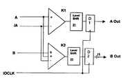
- a differential comparator K 1 compares signals A and /A to produce an output signal that is latched by a latch D 1 to produce an output data signal A Out.
- a level shift 21 is coupled to the output of comparator K 1 to remove shift in the logic low output level of the comparator due to the presence of common mode voltage on the input signals.
- Latch D 1 latches the output of level shift 21 on the rising edge of IOCLK (IOCLK is a clock signal derived such that data will be stable at the outputs of comparator K 1 when IOCLK rises).
- a novel singlential comparator K 2 receives the differential pair comprising signals A and /A as well as single-ended data signal B.
- Singlential comparator K 2 detects data signal B such that a common-mode voltage appearing on signals B, A, and /A is rejected.
- a level shift 23 couples the output of singlential comparator K 2 to a latch D 2 .
- Level shift 23 removes variations in the logic low voltage level on the output of singlential comparator K 2 due to the presence of common mode voltage on the input signals.
- level shift 23 is latched by latch D 2 which is clocked by the IOCLK signal and inverted by inverter II to produce a data output signal B Out. If data signal B is at a low logic level (corresponding to a lower voltage level), the output of singlential comparator K 2 will be at a high logic level, causing latch D 2 to latch a high logic level at its output and coupling a high logic level input to inverter I 1 .
- the result of the operation of the circuit of FIG. 2 is an A Out signal and a B Out signal that are very closely time-aligned, are representative of their corresponding A and B data input signals and have common mode error removed.
- N-channel transistor N 1 and N-channel transistor N 2 form a differential pair.
- N-channel transistor N 1 When the voltage of data signal A is higher than the voltage of complementary data signal /A, N-channel transistor N 1 will provide the majority of the current sourced into constant-current sink I 1 , causing the voltage at Out A to assume a high logic level.
- N-channel transistor N 2 Conversely when the voltage of data signal A is lower than the voltage of complementary data signal /A, N-channel transistor N 2 will provide the majority of the current sourced into constant-current sink I 1 , causing the voltage at Out A to assume a low logic level by drawing current through resistor R 1 which has a resistance value of R.
- the logic low output level of differential comparator K 1 is Vdd ⁇ IR where I is the current source magnitude and Vdd is the positive power supply voltage.
- I is the current source magnitude
- Vdd is the positive power supply voltage.
- N-channel transistors N 11 and N 12 form one side of a quasi-differential pair.
- N-channel transistor N 13 provides the other side of the quasi-differential pair.
- N-channel transistor N 13 will share current sourced into constant-current sink I 11 with the differential input transistor (N 11 or N 12 ) coupled to the differential input signal that is also at a high logic level.
- the current sourced through transistor N 13 causes the voltage at Out B to assume a low logic level by drawing current through resistor R 11 which has a resistance value of 2R.
- the transistor (N 11 or N 12 ) coupled to the differential input signal that is at a high logic level will conduct the majority of the current sourced into constant-current sink I 11 , causing the voltage at Out B to assume a high logic level.
- the logic low output level of singlential comparator K 2 is Vdd ⁇ IR where I is the current source magnitude and Vdd is the positive power supply voltage.
- Resistor R 11 is twice the value of the differential comparator K 1 output resistor R 1 , but transistor N 13 will only conduct approximately half of the current source I 11 current.
- the variation in logic low output level of comparator K 2 can be compensated for by using a level shifting circuit or by using a negative power supply rail that is below the desired logic low output voltage.
- resistor R 11 in raising the impedance of the current path through transistor N 13 over that of the transistor (N 11 or N 12 ) that is receiving a logic high gate input may be adjusted by sizing transistor N 13 slightly larger than transistors N 11 and N 12 .
- the singlential comparator thus removes common mode error by sharing current equally with a single-ended input stage when the single-ended input signal is in a high logic state and shunting current away from the single-ended input state when the single-ended input signal is in a low logic state. Since the sharing or shunting action of the differential input transistors is controlled by constant-current sink I 11 , common mode error is cancelled, since the shared current and the shunted current are substantially constant within a useable range of input signals.
- signals within the receiver of FIG. 2 are depicted in a timing diagram, and further illustrating the operation of the singlential comparator depicted in FIG. 3 B.
- data signal B and complementary data signal /A from the differential data signal pair are at a high voltage level with respect to data signal A from the differential data signal pair.
- Transistors N 13 and N 11 therefore share the current sourced into constant-current sink I 11 and the voltage drop across resistor R 11 will produce a logic low level at the output of singlential comparator K 2 .
- the output of singlential comparator K 2 is latched and inverted, resulting in a high logic level at B Out when IOCLK transitions to a high logic state at time T 1 .
- transistor N 12 When the differential data signal pair transitions to the opposite logic state just prior to time T 2 , transistor N 12 will share the current sourced into constant-current sink I 11 with transistor N 13 , maintaining the low logic level at the drain of transistor N 13 producing a logic low level at the output of singlential comparator K 2 , resulting in a high logic level output at B Out when IOCLK transitions again to a high logic level.
- transistor N 13 When single-ended signal B transitions to a logic low level and the differential data signal pair also transistions prior to time T 3 , transistor N 13 is turned off and the majority of the current sourced into constant-current sink I 11 is sourced by transistor N 11 .
- data signal B is depicted as returning to a high logic level, which will cause transistor N 13 to share current with transistor Nil producing a voltage drop across resistor R 11 and producing a logic low output from singlential comparator K 2 .
- time T 5 a drop in common-mode voltage is illustrated. Transistor N 13 will continue to share current equally with transistor N 11 and transistor N 12 will be turned more fully off due to the drop in common-mode voltage.
- Common-mode rejection is provided within the singlential comparator by the action of N-channel transistors N 11 and N 12 . Since the sum of the currents through transistors N 11 and N 12 represents the sum of the voltages at their inputs, it represents an average voltage, which is the common-mode voltage. As signal swing is reduced, the operation of singlential comparator K 2 becomes less effective in shunting current versus sharing current, but the averaging effect can maintain detection for lowered signal swings if the gain of singlential comparator K 2 is set at a high level by resistor R 11 and constant-current sink I 1 is operational for the low logic level input voltage.
- Other circuits may be implemented that derive an effective reference from a differential data signal and compare it to a single-ended data signal and thus constitute equivalent circuits for use within alternative embodiments of the present invention.
- the gain of the singlential comparator is set in part by resistor R 11 which has a value twice that of resistor R 1 within the differential comparator of FIG. 3 A. Since transistors N 11 and N 12 will effectively conduct twice the average current that a single transistor N 1 or N 2 of FIG. 3A would conduct, the doubled resistance of resistor R 11 over the resistance of R 1 raises the gain of the singlential comparator so that it is equal to the gain of the differential comparator of FIG. 3 A.
- the size of transistors N 1 and N 2 of FIG. 3 A and transistors N 11 , N 12 , and N 13 should be equal, so that the gain of the differential comparator and the singlential comparator are balanced.
- Differential comparator K 11 compares signals A and /A to produce data output signal A Out.
- a latch D 11 latches output of differential comparator K 11 on the rising edge of IOCLK (IOCLK is a clock signal derived such that data will be stable at the outputs of comparator K 11 when IOCLK rises).
- a second differential comparator K 12 compares data signal A with single-ended data signal B and a third differential comparator K 13 compares complementary data signal /A with single-ended data signal B.
- a latch D 12 latches output of differential comparator K 12 on the rising edge of IOCLK and a latch D 13 latches output of differential comparator K 13 on the rising edge of IOCLK.
- Data output B Out is provided by a multiplexer 42 that selects between the output of latch D 12 or latch D 13 .
- the selection is made by the output of a latch D 14 , which latches the output of an exclusive-OR gate XOR 14 .
- common-mode rejection is provided. For example, when data signals A and B are both in the same logic state, the output of comparator K 13 has the best common-mode rejection and therefore the output of latch D 13 should be selected by multiplexer 42 .
- the output of comparator K 12 has the best common-mode rejection and therefore the output of latch D 12 should be selected by multiplexer 42 .
- the circuit shown in FIG. 5 is designed for use with data signals that start the data cycle always in a logic low state. Thus prior to IOCLK rising, data signals A and B will be in a logic low state and complementary data signal /A will be in a logic high state.
- the logic network composed of exclusive-OR gates XOR 11 , XOR 12 , XOR 13 and XOR 14 create the selection signal latched by latch D 14 .
- Exclusive-OR gate XOR 11 detects the difference between the prior state of data signal A and the present state of data signal A, providing a change detect signal.
- exclusive-OR gate XOR 12 detects the difference between the prior state of the output of comparator K 12 and the present state of the output of comparator K 12 and exclusive-OR gate XOR 12 detects the difference between the prior state of the output of comparator K 13 and the present state of the output of comparator K 13 .
- the result of the operation of the circuit of FIG. 5 is an A Out signal and a B Out signal that are very closely time-aligned, are representative of their corresponding A and B data input signals and have common mode error removed.
Landscapes
- Engineering & Computer Science (AREA)
- Computer Hardware Design (AREA)
- Physics & Mathematics (AREA)
- Computing Systems (AREA)
- General Engineering & Computer Science (AREA)
- Mathematical Physics (AREA)
- Manipulation Of Pulses (AREA)
- Dc Digital Transmission (AREA)
Abstract
Description
Claims (17)
Priority Applications (2)
| Application Number | Priority Date | Filing Date | Title |
|---|---|---|---|
| US09/870,623 US6933752B2 (en) | 2001-05-31 | 2001-05-31 | Method and apparatus for interface signaling using single-ended and differential data signals |
| US10/616,012 US6922085B2 (en) | 2001-05-31 | 2003-07-08 | Comparator and method for detecting a signal using a reference derived from a differential data signal pair |
Applications Claiming Priority (1)
| Application Number | Priority Date | Filing Date | Title |
|---|---|---|---|
| US09/870,623 US6933752B2 (en) | 2001-05-31 | 2001-05-31 | Method and apparatus for interface signaling using single-ended and differential data signals |
Related Child Applications (1)
| Application Number | Title | Priority Date | Filing Date |
|---|---|---|---|
| US10/616,012 Division US6922085B2 (en) | 2001-05-31 | 2003-07-08 | Comparator and method for detecting a signal using a reference derived from a differential data signal pair |
Publications (2)
| Publication Number | Publication Date |
|---|---|
| US20020180480A1 US20020180480A1 (en) | 2002-12-05 |
| US6933752B2 true US6933752B2 (en) | 2005-08-23 |
Family
ID=25355799
Family Applications (2)
| Application Number | Title | Priority Date | Filing Date |
|---|---|---|---|
| US09/870,623 Expired - Lifetime US6933752B2 (en) | 2001-05-31 | 2001-05-31 | Method and apparatus for interface signaling using single-ended and differential data signals |
| US10/616,012 Expired - Fee Related US6922085B2 (en) | 2001-05-31 | 2003-07-08 | Comparator and method for detecting a signal using a reference derived from a differential data signal pair |
Family Applications After (1)
| Application Number | Title | Priority Date | Filing Date |
|---|---|---|---|
| US10/616,012 Expired - Fee Related US6922085B2 (en) | 2001-05-31 | 2003-07-08 | Comparator and method for detecting a signal using a reference derived from a differential data signal pair |
Country Status (1)
| Country | Link |
|---|---|
| US (2) | US6933752B2 (en) |
Cited By (9)
| Publication number | Priority date | Publication date | Assignee | Title |
|---|---|---|---|---|
| US20050213646A1 (en) * | 2004-01-27 | 2005-09-29 | Infineon Technologies Ag | xDSL-line-interface-circuit |
| US20060033535A1 (en) * | 2004-08-13 | 2006-02-16 | Nec Electronics Corporation | Signal detecting circuit |
| US7061277B1 (en) * | 2003-07-30 | 2006-06-13 | National Semiconductor Corporation | Low power differential-to-single-ended converter with good duty cycle performance |
| US7256652B1 (en) | 2005-09-08 | 2007-08-14 | Advanced Micro Devices, Inc. | Differential input receiver having over-voltage protection |
| US7656216B1 (en) * | 2008-02-13 | 2010-02-02 | Linear Technology Corporation | Method and system for determining a clock input mode |
| US10128906B2 (en) | 2016-07-11 | 2018-11-13 | Esker Technologies, LLC | Power line signal coupler |
| US10348418B1 (en) | 2014-07-22 | 2019-07-09 | Esker Technologies, LLC | Transient and spurious signal filter |
| US10417143B2 (en) * | 2015-10-08 | 2019-09-17 | Esker Technologies, LLC | Apparatus and method for sending power over synchronous serial communication wiring |
| US10560154B2 (en) | 2016-07-11 | 2020-02-11 | Esker Technologies, LLC | Power line signal coupler |
Families Citing this family (12)
| Publication number | Priority date | Publication date | Assignee | Title |
|---|---|---|---|---|
| US7243176B2 (en) * | 2004-11-05 | 2007-07-10 | Intel Corporation | Method and apparatus for power efficient and scalable memory interface |
| US7522670B2 (en) | 2005-02-03 | 2009-04-21 | International Business Machines Corporation | Digital transmission circuit and method providing selectable power consumption via single-ended or differential operation |
| US7353007B2 (en) * | 2005-02-03 | 2008-04-01 | International Business Machines Corporation | Digital transmission circuit and method providing selectable power consumption via multiple weighted drive slices |
| US7930492B2 (en) * | 2005-09-12 | 2011-04-19 | Samsung Electronics Co., Ltd. | Memory system having low power consumption |
| US7966446B2 (en) * | 2005-09-12 | 2011-06-21 | Samsung Electronics Co., Ltd. | Memory system and method having point-to-point link |
| US7245172B2 (en) * | 2005-11-08 | 2007-07-17 | International Business Machines Corporation | Level shifter apparatus and method for minimizing duty cycle distortion |
| US20080061842A1 (en) * | 2006-09-07 | 2008-03-13 | Micron Technology, Inc. | Circuit and method for detecting timed amplitude reduction of a signal relative to a threshold voltage |
| US7560959B2 (en) * | 2006-09-18 | 2009-07-14 | Micron Technology, Inc. | Absolute value peak differential voltage detector circuit and method |
| US7953162B2 (en) * | 2006-11-17 | 2011-05-31 | Intersil Americas Inc. | Use of differential pair as single-ended data paths to transport low speed data |
| FR2952488B1 (en) * | 2009-11-10 | 2011-12-09 | St Microelectronics Tours Sas | SENSOR CONNECTION CIRCUIT |
| US9270277B2 (en) * | 2012-06-28 | 2016-02-23 | Northwestern University | Emitter-coupled spin-transistor logic |
| US11190378B2 (en) * | 2018-04-09 | 2021-11-30 | Clearone, Inc. | Sending information signals on a differential signal pair |
Citations (6)
| Publication number | Priority date | Publication date | Assignee | Title |
|---|---|---|---|---|
| US3743856A (en) * | 1971-07-06 | 1973-07-03 | Signetics Corp | Exclusive-or ecl logic circuit |
| US4167727A (en) * | 1977-07-08 | 1979-09-11 | Motorola, Inc. | Logic circuits incorporating a dual function input |
| US4649301A (en) * | 1985-01-07 | 1987-03-10 | Thomson Components-Mostek Corp. | Multiple-input sense amplifier with two CMOS differential stages driving a high-gain stage |
| US4670673A (en) * | 1985-02-19 | 1987-06-02 | Advanced Micro Devices, Inc. | Multilevel differential ECL/CML gate circuit |
| US5936469A (en) * | 1997-08-04 | 1999-08-10 | Motorola, Inc. | Amplifier with input referred common-mode adjustment |
| US5936466A (en) * | 1997-08-04 | 1999-08-10 | International Business Machines Corporation | Differential operational transconductance amplifier |
-
2001
- 2001-05-31 US US09/870,623 patent/US6933752B2/en not_active Expired - Lifetime
-
2003
- 2003-07-08 US US10/616,012 patent/US6922085B2/en not_active Expired - Fee Related
Patent Citations (6)
| Publication number | Priority date | Publication date | Assignee | Title |
|---|---|---|---|---|
| US3743856A (en) * | 1971-07-06 | 1973-07-03 | Signetics Corp | Exclusive-or ecl logic circuit |
| US4167727A (en) * | 1977-07-08 | 1979-09-11 | Motorola, Inc. | Logic circuits incorporating a dual function input |
| US4649301A (en) * | 1985-01-07 | 1987-03-10 | Thomson Components-Mostek Corp. | Multiple-input sense amplifier with two CMOS differential stages driving a high-gain stage |
| US4670673A (en) * | 1985-02-19 | 1987-06-02 | Advanced Micro Devices, Inc. | Multilevel differential ECL/CML gate circuit |
| US5936469A (en) * | 1997-08-04 | 1999-08-10 | Motorola, Inc. | Amplifier with input referred common-mode adjustment |
| US5936466A (en) * | 1997-08-04 | 1999-08-10 | International Business Machines Corporation | Differential operational transconductance amplifier |
Cited By (11)
| Publication number | Priority date | Publication date | Assignee | Title |
|---|---|---|---|---|
| US7061277B1 (en) * | 2003-07-30 | 2006-06-13 | National Semiconductor Corporation | Low power differential-to-single-ended converter with good duty cycle performance |
| US20050213646A1 (en) * | 2004-01-27 | 2005-09-29 | Infineon Technologies Ag | xDSL-line-interface-circuit |
| US7801296B2 (en) * | 2004-01-27 | 2010-09-21 | Infineon Technologies Ag | xDSL-line-interface-circuit |
| US20060033535A1 (en) * | 2004-08-13 | 2006-02-16 | Nec Electronics Corporation | Signal detecting circuit |
| US7199620B2 (en) * | 2004-08-13 | 2007-04-03 | Nec Electronics Corporation | Signal detecting circuit |
| US7256652B1 (en) | 2005-09-08 | 2007-08-14 | Advanced Micro Devices, Inc. | Differential input receiver having over-voltage protection |
| US7656216B1 (en) * | 2008-02-13 | 2010-02-02 | Linear Technology Corporation | Method and system for determining a clock input mode |
| US10348418B1 (en) | 2014-07-22 | 2019-07-09 | Esker Technologies, LLC | Transient and spurious signal filter |
| US10417143B2 (en) * | 2015-10-08 | 2019-09-17 | Esker Technologies, LLC | Apparatus and method for sending power over synchronous serial communication wiring |
| US10128906B2 (en) | 2016-07-11 | 2018-11-13 | Esker Technologies, LLC | Power line signal coupler |
| US10560154B2 (en) | 2016-07-11 | 2020-02-11 | Esker Technologies, LLC | Power line signal coupler |
Also Published As
| Publication number | Publication date |
|---|---|
| US6922085B2 (en) | 2005-07-26 |
| US20020180480A1 (en) | 2002-12-05 |
| US20040051565A1 (en) | 2004-03-18 |
Similar Documents
| Publication | Publication Date | Title |
|---|---|---|
| US6933752B2 (en) | Method and apparatus for interface signaling using single-ended and differential data signals | |
| US7486112B2 (en) | Output buffer circuit with de-emphasis function | |
| US10200025B2 (en) | Pulse-amplitude modulated hybrid comparator circuit | |
| US7656321B2 (en) | Signaling system | |
| JP4578316B2 (en) | Transmitter | |
| US5504782A (en) | Current mode transmitter and receiver for reduced RFI | |
| US7411421B1 (en) | Apparatus and method for generating differential signal using single-ended drivers | |
| US20070099564A1 (en) | Current mode interface for off-chip high speed communication | |
| US8461882B2 (en) | Driver supporting multiple signaling modes | |
| US20120049897A1 (en) | Output buffer circuit and semiconductor device | |
| US7119600B2 (en) | Wide common mode high-speed differential receiver using thin and thick gate oxide MOSFETS in deep-submicron technology | |
| US7944252B1 (en) | High performance LVDS driver for scalable supply | |
| US8634500B2 (en) | Direct feedback equalization with dynamic referencing | |
| US7920014B2 (en) | Semiconductor integrated circuit device | |
| US6531896B1 (en) | Dual mode transmitter | |
| US6195397B1 (en) | Signal transmission and reception device for new wiring system | |
| US6690196B1 (en) | Simultaneous bi-directional I/O system | |
| US20160087817A1 (en) | Decision feedback equalizer summation circuit | |
| US6642748B2 (en) | Input circuit | |
| US20090232248A1 (en) | Data receiving device and semiconductor integrated circuit including such data receiving device | |
| US6771131B2 (en) | CMOS Amplifier for optoelectronic receivers | |
| US9455846B2 (en) | Decision feedback equalization | |
| JP2006148389A (en) | Signal transmission system | |
| KR100763603B1 (en) | improved low-voltage differential signaling circuit | |
| US6535032B2 (en) | Data receiver technology |
Legal Events
| Date | Code | Title | Description |
|---|---|---|---|
| AS | Assignment |
Owner name: INTERNATIONAL BUSINESS MACHINES CORPORATION, NEW Y Free format text: ASSIGNMENT OF ASSIGNORS INTEREST;ASSIGNORS:DREPS, DANIEL MARK;FERRAIOLO, FRANK DAVID;REEL/FRAME:011888/0540;SIGNING DATES FROM 20010530 TO 20010531 |
|
| FEPP | Fee payment procedure |
Free format text: PAYOR NUMBER ASSIGNED (ORIGINAL EVENT CODE: ASPN); ENTITY STATUS OF PATENT OWNER: LARGE ENTITY |
|
| STCF | Information on status: patent grant |
Free format text: PATENTED CASE |
|
| FPAY | Fee payment |
Year of fee payment: 4 |
|
| REMI | Maintenance fee reminder mailed | ||
| FPAY | Fee payment |
Year of fee payment: 8 |
|
| SULP | Surcharge for late payment |
Year of fee payment: 7 |
|
| AS | Assignment |
Owner name: GLOBALFOUNDRIES U.S. 2 LLC, NEW YORK Free format text: ASSIGNMENT OF ASSIGNORS INTEREST;ASSIGNOR:INTERNATIONAL BUSINESS MACHINES CORPORATION;REEL/FRAME:036550/0001 Effective date: 20150629 |
|
| AS | Assignment |
Owner name: GLOBALFOUNDRIES INC., CAYMAN ISLANDS Free format text: ASSIGNMENT OF ASSIGNORS INTEREST;ASSIGNORS:GLOBALFOUNDRIES U.S. 2 LLC;GLOBALFOUNDRIES U.S. INC.;REEL/FRAME:036779/0001 Effective date: 20150910 |
|
| FPAY | Fee payment |
Year of fee payment: 12 |
|
| AS | Assignment |
Owner name: WILMINGTON TRUST, NATIONAL ASSOCIATION, DELAWARE Free format text: SECURITY AGREEMENT;ASSIGNOR:GLOBALFOUNDRIES INC.;REEL/FRAME:049490/0001 Effective date: 20181127 |
|
| AS | Assignment |
Owner name: GLOBALFOUNDRIES U.S. INC., CALIFORNIA Free format text: ASSIGNMENT OF ASSIGNORS INTEREST;ASSIGNOR:GLOBALFOUNDRIES INC.;REEL/FRAME:050122/0001 Effective date: 20190821 |
|
| AS | Assignment |
Owner name: MARVELL INTERNATIONAL LTD., BERMUDA Free format text: ASSIGNMENT OF ASSIGNORS INTEREST;ASSIGNOR:GLOBALFOUNDRIES U.S. INC.;REEL/FRAME:051070/0625 Effective date: 20191105 |
|
| AS | Assignment |
Owner name: CAVIUM INTERNATIONAL, CAYMAN ISLANDS Free format text: ASSIGNMENT OF ASSIGNORS INTEREST;ASSIGNOR:MARVELL INTERNATIONAL LTD.;REEL/FRAME:052918/0001 Effective date: 20191231 |
|
| AS | Assignment |
Owner name: MARVELL ASIA PTE, LTD., SINGAPORE Free format text: ASSIGNMENT OF ASSIGNORS INTEREST;ASSIGNOR:CAVIUM INTERNATIONAL;REEL/FRAME:053475/0001 Effective date: 20191231 |
|
| AS | Assignment |
Owner name: GLOBALFOUNDRIES INC., CAYMAN ISLANDS Free format text: RELEASE BY SECURED PARTY;ASSIGNOR:WILMINGTON TRUST, NATIONAL ASSOCIATION;REEL/FRAME:054636/0001 Effective date: 20201117 |