US6462521B1 - High-speed charge-mode controller for a multi-phase switched-mode power converter - Google Patents
High-speed charge-mode controller for a multi-phase switched-mode power converter Download PDFInfo
- Publication number
- US6462521B1 US6462521B1 US09/908,007 US90800701A US6462521B1 US 6462521 B1 US6462521 B1 US 6462521B1 US 90800701 A US90800701 A US 90800701A US 6462521 B1 US6462521 B1 US 6462521B1
- Authority
- US
- United States
- Prior art keywords
- current
- phase
- accordance
- converter
- signal
- Prior art date
- Legal status (The legal status is an assumption and is not a legal conclusion. Google has not performed a legal analysis and makes no representation as to the accuracy of the status listed.)
- Expired - Fee Related
Links
Images


Classifications
-
- H—ELECTRICITY
- H02—GENERATION; CONVERSION OR DISTRIBUTION OF ELECTRIC POWER
- H02M—APPARATUS FOR CONVERSION BETWEEN AC AND AC, BETWEEN AC AND DC, OR BETWEEN DC AND DC, AND FOR USE WITH MAINS OR SIMILAR POWER SUPPLY SYSTEMS; CONVERSION OF DC OR AC INPUT POWER INTO SURGE OUTPUT POWER; CONTROL OR REGULATION THEREOF
- H02M3/00—Conversion of dc power input into dc power output
- H02M3/02—Conversion of dc power input into dc power output without intermediate conversion into ac
- H02M3/04—Conversion of dc power input into dc power output without intermediate conversion into ac by static converters
- H02M3/10—Conversion of dc power input into dc power output without intermediate conversion into ac by static converters using discharge tubes with control electrode or semiconductor devices with control electrode
- H02M3/145—Conversion of dc power input into dc power output without intermediate conversion into ac by static converters using discharge tubes with control electrode or semiconductor devices with control electrode using devices of a triode or transistor type requiring continuous application of a control signal
- H02M3/155—Conversion of dc power input into dc power output without intermediate conversion into ac by static converters using discharge tubes with control electrode or semiconductor devices with control electrode using devices of a triode or transistor type requiring continuous application of a control signal using semiconductor devices only
- H02M3/156—Conversion of dc power input into dc power output without intermediate conversion into ac by static converters using discharge tubes with control electrode or semiconductor devices with control electrode using devices of a triode or transistor type requiring continuous application of a control signal using semiconductor devices only with automatic control of output voltage or current, e.g. switching regulators
- H02M3/158—Conversion of dc power input into dc power output without intermediate conversion into ac by static converters using discharge tubes with control electrode or semiconductor devices with control electrode using devices of a triode or transistor type requiring continuous application of a control signal using semiconductor devices only with automatic control of output voltage or current, e.g. switching regulators including plural semiconductor devices as final control devices for a single load
- H02M3/1584—Conversion of dc power input into dc power output without intermediate conversion into ac by static converters using discharge tubes with control electrode or semiconductor devices with control electrode using devices of a triode or transistor type requiring continuous application of a control signal using semiconductor devices only with automatic control of output voltage or current, e.g. switching regulators including plural semiconductor devices as final control devices for a single load with a plurality of power processing stages connected in parallel
Definitions
- the present invention is directed to a high-speed charge-mode controller for use with a switched-mode power converter.
- Power converters are used in modem electronic equipment to convert relatively poorly regulated direct current (DC) power supply voltages to highly regulated DC power supply voltages. Such devices are used, for example, to power microprocessors and similar devices. Current technology microprocessors can require 1.5 volts or less of supply voltage at peak levels exceeding 80 amperes (A). Because such devices are often switched at rates exceeding 1.5 GHz, they routinely experience current slew rates of 400 A/microsecond ( ⁇ Sec) or more. As a result, it has become necessary in recent years to provide such devices with power from a multi-phase voltage regulator. The multi-phase voltage regulator typically obtains its power from a single relatively poorly regulated power supply and provides a number of sources (phases) of highly regulated voltage for use by the device.
- phase currents are automatically balanced; (2) active voltage positioning is easily implemented with very good precision; (3) the wide control bandwidth settles the output to its correct position very quickly; and (4) module current sharing can be implemented.
- PICM has these merits, it also has some shortcomings. These are: (1) the leading edge spike of the MOSFET (metal oxide semiconductor field effect transistor) current needs to be filtered out; (2) parasitics in the layout tend to interact with the sensing filter to cause ringing and limit operational frequencies to about 500 KHz per phase at 5 volts input and 250 KHz per phase at 12 volts input; (3) in order to avoid overlapping of the current pulses coming from different phases (a requirement of this approach) multiple sensing resistors and current amplifiers are required. This last shortcoming adds to system cost and IC (integrated circuit) pin count.
- MOSFET metal oxide semiconductor field effect transistor
- the maximum duty cycle of the PWM (pulse with modulation) pulses is also limited depending on the configuration to less than 50% for a two-phase controller, less than 33% for a three-phase controller, etc. This limits the applications in which such a controller may be used.
- a multiphase controller for a PWM power converter employs a single current sense device to measure input current, I, and an integrator at each phase to accurately measure power delivered during a pulse.
- the integrator monitors current delivered through a circuit which delivers a current signal scaled to I/N where N is the number of active phases. Thus where there are three overlapping phases, one-third of I is delivered to the integrator for each phase that is on or active.
- the integrator provides a Charge Ramp signal to an input of a Pulse Width Modulation (PWM) comparator associated with each phase.
- PWM Pulse Width Modulation
- the other input of the PWM comparator is tied to an error control signal common to all of the phases. When the Charge Ramp signal and the error control signal match, the corresponding phase is turned off for the duration of the cycle.
- FIG. 1 is an electrical schematic diagram of a typical application circuit employing a high-speed charge-mode, multi-phase power converter in accordance with an embodiment of the present invention.
- FIG. 2 is a simulation circuit illustrating the operation of an IICM (integrated input current mode) power converter circuit. This circuit is implemented as a 250 KHz three-phase five-volt input 1.6 ⁇ 80 mv output 45A buck-type voltage converter.
- FIG. 3 is an electrical schematic diagram of the charge mode controller in accordance with one embodiment of the present invention.
- FIG. 4 is an electrical schematic diagram of one instantiation of the charge storing generation block of the charge mode controller of FIG. 3 .
- FIG. 5A is a plot of current vs. time for the instantaneous current in the top MOSFET of one phase of a PWM power converter in accordance with the embodiment of FIG. 2 .
- FIG. 5B is a plot of current vs. time for the current in the sensing resistor R 12 of FIG. 2 .
- FIG. 5C is a plot of voltage vs. time for the voltage across the current sensing input pins IS+, IS ⁇ of FIG. 2 .
- FIG. 5D is a plot of voltage vs. time for the filtered voltage of the Charge Ramp signal used in accordance with the embodiment of FIG. 2 as filtered by C 9 and R 15 .
- FIG. 6A is a plot of current vs. time for the current passing through MOSFETs MPL 2 ( 82 ), MPL 3 ( 84 ) and MPL 4 ( 86 ) of FIG. 4 for one phase in a no-phase-overlap case. Note that the current through MPL 3 and MPL 4 is always zero in this case.
- FIG. 6B is a plot of voltage vs. time for the voltages 88 , 90 , 92 ,across the drain to source of the low side MOSFETs (or “phase nodes”) 138 , 140 , 142 of the three phases 88 , 90 , 92 .
- FIG. 7A is a plot of current vs. time for the current passing through MOSFETs MPL 2 ( 94 ), MPL 3 ( 96 ) and MPL 4 ( 98 ) of FIG. 4 for a two-phase-overlap case. Note that the current through MPL 4 is always zero in this case.
- FIG. 7B is a plot of voltage vs. time for the voltage across the phase nodes 138 , 140 , 142 of the three phases 100 , 102 104 .
- FIG. 8A is a plot of current vs. time for the current passing through MOSFETs MPL 2 ( 106 ), MPL 3 ( 108 ) and MPL 4 ( 110 ) of FIG. 4 in a three-phase overlap case.
- FIG. 8B is a plot of voltage vs. time for the voltage across the phase nodes 138 , 140 , 142 of the three phases 112 , 114 and 116 and also illustrating the Charge Ramp signal for phase 1 ( 118 ).
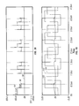
- FIG. 9A is a plot of voltage vs. time for the three Charge Ramp signals 120 , 122 , 124 which are the outputs of the integrators.
- FIG. 9B is a plot of current vs. time for the current flow through the input sensing resistor R 12 .
- FIG. 9C is a plot of current vs. time for the output inductor currents taken at nodes 126 , 128 and 130 of FIG. 2 .
- the corresponding traces are 132 , 134 and 136 .
- FIG. 9D is a plot of voltage vs. time for the three phase nodes 138 , 140 , 142 of FIG. 2 .
- FIG. 9E is a plot of voltage vs. time for the overall voltage output of the power converter. Note that the converter transitions from no load at 80 ⁇ S-100 ⁇ S to full load at 100 ⁇ S-200 ⁇ S and back to no load at 200 ⁇ S-220 ⁇ S.
- Embodiments of the present invention are described herein in the context of a high-speed charge-mode controller for a multi-phase switched mode power converter. Those of ordinary skill in the art will realize that the following detailed description of the present invention is illustrative only and is not intended to be in any way limiting. Other embodiments of the present invention will readily suggest themselves to such skilled persons having the benefit of this disclosure. Reference will now be made in detail to implementations of the present invention as illustrated in the accompanying drawings. The same reference indicators will be used throughout the drawings and the following detailed description to refer to the same or like parts.
- FIG. 1 is an electrical schematic diagram of a typical application circuit 10 employing a high-speed charge mode controller 12 for a multi-phase switched mode power converter.
- the example circuit 10 includes a number of inputs 14 , a current sense resistor R 19 ( 16 ), driver circuits H 51 , H 52 , H 53 and H 54 for the four phases shown, and pulse width modulation (PWM) MOSFET pairs 18 , 20 , 22 and 24 corresponding to each driver circuit.
- Example circuit 10 also includes conventional filter circuitry 26 and provides a highly regulated output voltage at pin 28 .
- FIG. 2 is a simulation circuit 50 illustrating the operation of an IICM (integrated input current mode) power converter circuit in accordance with one embodiment of the present invention.
- This circuit is implemented as a 250 KHz three-phase five-volt input 1.6 ⁇ 80 mV output 45A buck-type voltage converter.
- Total input current is sensed at R 12 ( 52 ) and delivered to controller 54 via pins designated IS+ and IS ⁇ .
- R 12 has a resistance in a range of about 0.002 ohms to about 0.005 ohms.
- Controller 54 may be a single integrated circuit but is not required to be. Controller 54 may provide output pins for each desired phase or may have extra unused output pins. Voltage reference is provided by a highly precise conventional band gap source.
- FIG. 3 is an electrical schematic diagram of the charge mode controller 54 of FIG. 2 is accordance with one embodiment of the present invention. This diagram is also shown as a simulation circuit.
- a conventional band gap reference plus error amplifier circuit 56 provides an error voltage signal which is used to turn off the various phases when they have achieved a desired phase during a particular cycle of operation.
- Charge steering circuits 58 a , 58 b and 58 c each have inputs P 1 , P 2 and P 3 which correspond to the turn-on logic signal of phases 1 , 2 and 3 , respectively. They. also receive Vdd (the input voltage signal), I_sense (a signal proportional to the sensed current) and produce a Charge Ramp signal.
- This charge ramp signal is applied at each phase to a comparator ( 60 a , 60 b , 60 c ) with the error signal and the comparator turns off the phase when the error signal and the Charge Ramp signal are equal.
- Flip flops U 1 , U 2 and U 2 (or equivalent circuitry well known to those of ordinary skill in the art) hold the OUT 1 , OUT 2 and OUT 3 signals high until cleared by comparators 60 a , 60 b and 60 c , respectively.
- Clock signals V_CLK 1 , V_CLK 2 and V_CLK 3 turn on flip flops U 1 , U 2 and U 3 at the beginning of each respective cycle in a conventional manner.
- FIG. 4 is an electrical schematic diagram (also in simulation form) of one instantiation of the charge steering generation block for phase P 1 of the charge-mode controller of FIG. 3 .
- each of the other phases has a similar, though not identical, block, i.e., substitute P 1 for P 2 , P 2 for P 3 , P 3 for P 1 for the P 2 block, etc.
- This circuit includes four main blocks.
- the first block is a current level decoder 62 which takes logic inputs P 1 , P 2 and P 3 , any of which may be “on” or “off” and provides outputs G 11 , G 12 and G 13 where G 11 is asserted if only one of the three phases P 1 , P 2 and P 3 is “on”, G 12 is asserted if two of the three phases are “on”, G 13 is asserted if all three phases are “on”, and none of G 11 , G 12 and G 13 are asserted if all three phases are “off”.
- the logic circuit of decoder 62 is one example of how to perform this function. Many other ways of performing this function are available and more or fewer phases may be implemented as will now be apparent to those of ordinary skill in the art.
- the second block is a current mirror block 64 which generates a current I at node 66 which is proportional to I_sense; The same current I is generated at node 68 .
- a current I/2 is generated at node 70 and a current I/3 is generated at node 72 .
- the third block is a current selector block 74 .
- Current selector block receives I from node 68 , I/2 from node 70 and I/3 from node 72 . It gates each of these current sources with the signals G 11 , G 12 and G 13 , respectively, from current level decoder block 62 .
- G 11 is asserted and turns on MOSFET MPL 2 allowing current I to pass to node 76
- G 12 is asserted and turns on MOSFET MPL 3 allowing I/2 to pass to node 76 .
- MOSFET MPL 4 is turned on and I/3 passes to node 76 . In this way, the current passed to node 76 at any moment is scaled with the number of phases in use at that moment.
- the fourth block is a Charge Ramp block 78 which provides a charge ramp signal representing an integration via capacitor C 2 of the charge received at node 76 .
- P 1 is deasserted by comparator 60 a (FIG. 4)
- switch MNL 1 is turned on to discharge C 2 until the next cycle.
- the accumulated voltage on C 2 appears at output “Ramp”.
- an appropriate filter as well known to those of ordinary skill in the art should also be included as shown, for example, in FIG. 2 .
- FIGS. 5A-11E illustrate operational characteristics of a power converter built in accordance with the principles shown herein.
- FIG. 5A is a plot of current vs. time for the instantaneous current in the top MOSFET of one phase of a PWM power converter in accordance with the embodiment of FIG. 2 .
- a leading edge spike 80 is typically present due to MOSFET switching transients. This needs to be filtered out in PICM-type voltage regulators to avoid erroneous operation. In the present approach there is no requirement that it be filtered out.
- FIG. 5B is a plot of current vs. time for the current in the sensing resistor R 12 of FIG. 2 . Due to circuit parasitics, a switching frequency noise is superimposed on the high-side MOSFET current signal which provides a very distorted signal for PICM-type voltage regulation. The present invention avoids this problem.
- FIG. 5C is a plot of voltage vs. time for the voltage across the current sensing input pins IS+, IS ⁇ of FIG. 2 .
- FIG. 5D is a plot of voltage vs. time for the voltage of the Charge Ramp signal used in accordance with the embodiment of FIG. 2 as filtered by C 9 and R 15 .
- This Charge Ramp signal is based on charge integration and greatly reduces the noise caused by the leading edge spike and switching.
- the Charge Ramp signal can therefore be used as a good quality PWM carrier signal. As a result, one can operate the PWM converter at a much higher switching frequency than before, e.g., in excess of 500 KHz.
- FIG. 6A is a plot of current vs. time for the current passing through MOSFETs MPL 2 ( 82 ), MPL 3 ( 84 ) and MPL 4 ( 86 ) of FIG. 4 for one phase in a no-phase-overlap case. Note that the current through MPL 3 and MPL 4 is always zero in this case.
- FIG. 6B is a plot of voltage vs. time for the voltages 88 , 90 , 92 across the phase nodes 138 , 140 and 142 of FIG. 2 for the case of FIG. 6 A.
- FIG. 7A is a plot of current vs. time for the current passing through MOSFETs MPL 2 ( 94 ), MPL 3 ( 96 ) and MPL 4 ( 98 ) of FIG. 4 for a two-phase-overlap case. Note current through MPL 4 is always zero in this case.
- FIG. 7B is a plot of voltage vs. time for the voltage across the phase nodes 138 , 140 and 142 of FIG. 2 for the case of FIG. 7 A.
- FIG. 8A is a plot of current vs. time for the current passing through MOSFETs MPL 29 ( 106 ), MPL 3 ( 108 ) and MPL 4 ( 10 ) of FIG. 4 in a three-phase overlap case.
- FIG. 8B is a plot of voltage vs. time for the voltage across the phase nodes 138 , 140 and 142 of FIG. 2 for the case of FIG. 8 A.
- FIG. 9A is a plot of voltage vs. time for the Charge Ramp signals which are outputs of the integrators.
- FIG. 9B is a plot of current vs. time for the current through sensing resistor R 12 .
- FIG. 9C is a plot of current vs. time for the output inductor currents taken at nodes 126 , 128 and 130 of FIG. 2 .
- the corresponding traces are 132 , 134 and 136 .
- FIG. 9D is a plot of voltage vs. time for the phase nodes 138 , 140 and 142 of FIG. 2 .
- FIG. 9E is a plot of voltage vs. time for the overall voltage output of the power converter. Note that the converter transitions from no load at 80 ⁇ S-100 ⁇ S to full load at 100 ⁇ S-200 ⁇ S and-back to no load at 200 ⁇ S-220 ⁇ S.
- the present invention is not limited to use in buck converter circuits and will find use in many types of power converter circuits. While the present invention is primarily intended for use in multi-phase converters, it will operate in a single phase environment, a two-phase environment, etc., as desired by the circuit designer.
Abstract
Description
Claims (32)
Priority Applications (1)
| Application Number | Priority Date | Filing Date | Title |
|---|---|---|---|
| US09/908,007 US6462521B1 (en) | 2001-07-17 | 2001-07-17 | High-speed charge-mode controller for a multi-phase switched-mode power converter |
Applications Claiming Priority (1)
| Application Number | Priority Date | Filing Date | Title |
|---|---|---|---|
| US09/908,007 US6462521B1 (en) | 2001-07-17 | 2001-07-17 | High-speed charge-mode controller for a multi-phase switched-mode power converter |
Publications (1)
| Publication Number | Publication Date |
|---|---|
| US6462521B1 true US6462521B1 (en) | 2002-10-08 |
Family
ID=25425007
Family Applications (1)
| Application Number | Title | Priority Date | Filing Date |
|---|---|---|---|
| US09/908,007 Expired - Fee Related US6462521B1 (en) | 2001-07-17 | 2001-07-17 | High-speed charge-mode controller for a multi-phase switched-mode power converter |
Country Status (1)
| Country | Link |
|---|---|
| US (1) | US6462521B1 (en) |
Cited By (13)
| Publication number | Priority date | Publication date | Assignee | Title |
|---|---|---|---|---|
| US20020105009A1 (en) * | 2000-07-13 | 2002-08-08 | Eden Richard C. | Power semiconductor switching devices, power converters, integrated circuit assemblies, integrated circuitry, power current switching methods, methods of forming a power semiconductor switching device, power conversion methods, power semiconductor switching device packaging methods, and methods of forming a power transistor |
| US20030178975A1 (en) * | 2002-03-22 | 2003-09-25 | George Schuellein | Multi-phase buck converter |
| US20030201761A1 (en) * | 2002-03-29 | 2003-10-30 | Intersil Americas Inc., State Of Incorporation: Delaware | Method and circuit for scaling and balancing input and output currents in a multi-phase DC-DC converter using different input voltages |
| US20040151010A1 (en) * | 2001-06-25 | 2004-08-05 | Ragnar Jonsson | Multiple stage switch circuit |
| US20050184717A1 (en) * | 2004-02-19 | 2005-08-25 | Mike Walters | DC-DC regulator with switching frequency responsive to load |
| US20060091869A1 (en) * | 2004-11-01 | 2006-05-04 | Linear Technology Corporation | Method of and system for regulating a power supply |
| US7075346B1 (en) | 2004-11-12 | 2006-07-11 | National Semiconductor Corporation | Synchronized frequency multiplier for multiple phase PWM control switching regulator without using a phase locked loop |
| US7109689B2 (en) * | 2003-04-04 | 2006-09-19 | Intersil Americas Inc. | Transient-phase PWM power supply and method |
| WO2007064694A2 (en) * | 2005-11-30 | 2007-06-07 | Semtech Corporation | High efficiency power supply for led lighting applications |
| US7265522B2 (en) | 2003-09-04 | 2007-09-04 | Marvell World Trade Ltd. | Dynamic multiphase operation |
| US20070236205A1 (en) * | 2006-02-28 | 2007-10-11 | Stmicroelectronics S.R.I. | Method for controlling a multiphase interleaving converter and corresponding controller |
| US20120286769A1 (en) * | 2011-05-12 | 2012-11-15 | Stmicroelectronics S.R.L. | Current sensing device for a multi-phase switched voltage regulator |
| US9431838B2 (en) | 2013-03-15 | 2016-08-30 | Integrated Device Technology, Inc. | Apparatuses and related methods for charging control of a switching voltage regulator |
Citations (10)
| Publication number | Priority date | Publication date | Assignee | Title |
|---|---|---|---|---|
| US4821297A (en) * | 1987-11-19 | 1989-04-11 | American Telephone And Telegraph Company, At&T Bell Laboratories | Digital phase locked loop clock recovery scheme |
| US5278489A (en) * | 1992-05-29 | 1994-01-11 | Scitex Digital Printing, Inc. | Multi-phase switching power supply |
| US5477132A (en) * | 1992-01-10 | 1995-12-19 | Space Systems/Loral, Inc. | Multi-sectioned power converter having current-sharing controller |
| US5712540A (en) * | 1994-07-26 | 1998-01-27 | Fujitsu General Limited | Control method and apparatus for controlling motors of air conditioner |
| US5831837A (en) * | 1995-02-28 | 1998-11-03 | International Business Machines Corporation | Switch mode power supply |
| US6137274A (en) * | 2000-02-02 | 2000-10-24 | National Semiconductor Corporation | Switching DC-to-DC converter and conversion method with current sharing between paralleled channels |
| US6198261B1 (en) * | 1998-10-30 | 2001-03-06 | Volterra Semiconductor Corporation | Method and apparatus for control of a power transistor in a digital voltage regulator |
| US6215290B1 (en) * | 1999-11-15 | 2001-04-10 | Semtech Corporation | Multi-phase and multi-module power supplies with balanced current between phases and modules |
| US6278263B1 (en) * | 1999-09-01 | 2001-08-21 | Intersil Corporation | Multi-phase converter with balanced currents |
| US6362608B1 (en) * | 2001-02-01 | 2002-03-26 | Maxim Integrated Products, Inc. | Multi-phase switching converters and methods |
-
2001
- 2001-07-17 US US09/908,007 patent/US6462521B1/en not_active Expired - Fee Related
Patent Citations (10)
| Publication number | Priority date | Publication date | Assignee | Title |
|---|---|---|---|---|
| US4821297A (en) * | 1987-11-19 | 1989-04-11 | American Telephone And Telegraph Company, At&T Bell Laboratories | Digital phase locked loop clock recovery scheme |
| US5477132A (en) * | 1992-01-10 | 1995-12-19 | Space Systems/Loral, Inc. | Multi-sectioned power converter having current-sharing controller |
| US5278489A (en) * | 1992-05-29 | 1994-01-11 | Scitex Digital Printing, Inc. | Multi-phase switching power supply |
| US5712540A (en) * | 1994-07-26 | 1998-01-27 | Fujitsu General Limited | Control method and apparatus for controlling motors of air conditioner |
| US5831837A (en) * | 1995-02-28 | 1998-11-03 | International Business Machines Corporation | Switch mode power supply |
| US6198261B1 (en) * | 1998-10-30 | 2001-03-06 | Volterra Semiconductor Corporation | Method and apparatus for control of a power transistor in a digital voltage regulator |
| US6278263B1 (en) * | 1999-09-01 | 2001-08-21 | Intersil Corporation | Multi-phase converter with balanced currents |
| US6215290B1 (en) * | 1999-11-15 | 2001-04-10 | Semtech Corporation | Multi-phase and multi-module power supplies with balanced current between phases and modules |
| US6137274A (en) * | 2000-02-02 | 2000-10-24 | National Semiconductor Corporation | Switching DC-to-DC converter and conversion method with current sharing between paralleled channels |
| US6362608B1 (en) * | 2001-02-01 | 2002-03-26 | Maxim Integrated Products, Inc. | Multi-phase switching converters and methods |
Cited By (30)
| Publication number | Priority date | Publication date | Assignee | Title |
|---|---|---|---|---|
| US6737301B2 (en) | 2000-07-13 | 2004-05-18 | Isothermal Systems Research, Inc. | Power semiconductor switching devices, power converters, integrated circuit assemblies, integrated circuitry, power current switching methods, methods of forming a power semiconductor switching device, power conversion methods, power semiconductor switching device packaging methods, and methods of forming a power transistor |
| US7019337B2 (en) | 2000-07-13 | 2006-03-28 | Isothermal Systems Research, Inc. | Power semiconductor switching devices, power converters, integrated circuit assemblies, integrated circuitry, power current switching methods, methods of forming a power semiconductor switching device, power conversion methods, power semiconductor switching device packaging methods, and methods of forming a power transistor |
| US20050230746A1 (en) * | 2000-07-13 | 2005-10-20 | Eden Richard C | Power semiconductor switching devices and power semiconductor devices |
| US20020105009A1 (en) * | 2000-07-13 | 2002-08-08 | Eden Richard C. | Power semiconductor switching devices, power converters, integrated circuit assemblies, integrated circuitry, power current switching methods, methods of forming a power semiconductor switching device, power conversion methods, power semiconductor switching device packaging methods, and methods of forming a power transistor |
| US6710441B2 (en) | 2000-07-13 | 2004-03-23 | Isothermal Research Systems, Inc. | Power semiconductor switching devices, power converters, integrated circuit assemblies, integrated circuitry, power current switching methods, methods of forming a power semiconductor switching device, power conversion methods, power semiconductor switching device packaging methods, and methods of forming a power transistor |
| US20040151010A1 (en) * | 2001-06-25 | 2004-08-05 | Ragnar Jonsson | Multiple stage switch circuit |
| US6940736B2 (en) * | 2001-06-25 | 2005-09-06 | Joensson Ragnar | Multiple switch circuit with limited switch frequency |
| US6806689B2 (en) | 2002-03-22 | 2004-10-19 | International Rectifier Corporation | Multi-phase buck converter |
| WO2003083596A1 (en) * | 2002-03-22 | 2003-10-09 | International Rectifier Corporation | Multi-phase buck converter |
| US20030178975A1 (en) * | 2002-03-22 | 2003-09-25 | George Schuellein | Multi-phase buck converter |
| US6897636B2 (en) | 2002-03-29 | 2005-05-24 | Intersil Americas Inc. | Method and circuit for scaling and balancing input and output currents in a multi-phase DC-DC converter using different input voltages |
| US20030201761A1 (en) * | 2002-03-29 | 2003-10-30 | Intersil Americas Inc., State Of Incorporation: Delaware | Method and circuit for scaling and balancing input and output currents in a multi-phase DC-DC converter using different input voltages |
| US7109689B2 (en) * | 2003-04-04 | 2006-09-19 | Intersil Americas Inc. | Transient-phase PWM power supply and method |
| US7479766B2 (en) | 2003-09-04 | 2009-01-20 | Marvell World Trade Ltd. | Dynamic multiphase operation |
| US7696732B2 (en) | 2003-09-04 | 2010-04-13 | Marvell World Trade Ltd. | Dynamic multiphase operation |
| US7265522B2 (en) | 2003-09-04 | 2007-09-04 | Marvell World Trade Ltd. | Dynamic multiphase operation |
| US20090174374A1 (en) * | 2003-09-04 | 2009-07-09 | Sehat Sutardja | Dynamic multiphase operation |
| US20070296382A1 (en) * | 2003-09-04 | 2007-12-27 | Sehat Sutardja | Dynamic multiphase operation |
| US7208921B2 (en) | 2004-02-19 | 2007-04-24 | International Rectifier Corporation | DC-DC regulator with switching frequency responsive to load |
| US20050184717A1 (en) * | 2004-02-19 | 2005-08-25 | Mike Walters | DC-DC regulator with switching frequency responsive to load |
| US20060091869A1 (en) * | 2004-11-01 | 2006-05-04 | Linear Technology Corporation | Method of and system for regulating a power supply |
| US7075346B1 (en) | 2004-11-12 | 2006-07-11 | National Semiconductor Corporation | Synchronized frequency multiplier for multiple phase PWM control switching regulator without using a phase locked loop |
| WO2007064694A3 (en) * | 2005-11-30 | 2009-05-14 | Semtech Corp | High efficiency power supply for led lighting applications |
| WO2007064694A2 (en) * | 2005-11-30 | 2007-06-07 | Semtech Corporation | High efficiency power supply for led lighting applications |
| US20070236205A1 (en) * | 2006-02-28 | 2007-10-11 | Stmicroelectronics S.R.I. | Method for controlling a multiphase interleaving converter and corresponding controller |
| US9467042B2 (en) | 2006-02-28 | 2016-10-11 | Stmicroelectronics S.R.1. | Method for controlling a multiphase interleaving converter and corresponding controller |
| US9780649B2 (en) | 2006-02-28 | 2017-10-03 | Stmicroelectronics S.R.L. | Method for controlling a multiphase interleaving converter and corresponding controller |
| US20120286769A1 (en) * | 2011-05-12 | 2012-11-15 | Stmicroelectronics S.R.L. | Current sensing device for a multi-phase switched voltage regulator |
| US9203315B2 (en) * | 2011-05-12 | 2015-12-01 | Stmicroelectronics S.R.L. | Current sensing device for a multi-phase switched voltage regulator |
| US9431838B2 (en) | 2013-03-15 | 2016-08-30 | Integrated Device Technology, Inc. | Apparatuses and related methods for charging control of a switching voltage regulator |
Similar Documents
| Publication | Publication Date | Title |
|---|---|---|
| US6912144B1 (en) | Method and apparatus for adjusting current amongst phases of a multi-phase converter | |
| US7209371B2 (en) | Method and apparatus for extending the operating range of a flyforward converter | |
| US7109691B2 (en) | Systems for auto-interleaving synchronization in a multiphase switching power converter | |
| US7936540B2 (en) | DC-DC converters having improved current sensing and related methods | |
| US7005835B2 (en) | Method and apparatus for load sharing in a multiphase switching power converter | |
| US7339361B2 (en) | Multi-phase DC-DC converter using auxiliary resistor network to feed back multiple single-ended sensed currents to supervisory controller for balanced current-sharing among plural channels | |
| US6462521B1 (en) | High-speed charge-mode controller for a multi-phase switched-mode power converter | |
| US7615982B1 (en) | Power converter able to rapidly respond to fast changes in load current | |
| US20070085523A1 (en) | Dc-dc converter | |
| US7589509B2 (en) | Switching regulator | |
| US6836103B2 (en) | Method and apparatus for dithering auto-synchronization of a multiphase switching power converter | |
| US20030214274A1 (en) | Multiple-phase power converter having current sharing and high frequency filtering | |
| CN110620574A (en) | System and method for driving a power switch in combination with a regulated DI/DT and/or DV/DT | |
| US10193449B2 (en) | Buck voltage converter | |
| US20030035260A1 (en) | Integrated circuit for generating a plurality of direct current (DC) output voltages | |
| JP4251021B2 (en) | Power supply device and hard disk device and IC using the same | |
| JP2018521622A (en) | Circuit and method for controlling a boost switching regulator based on inductor current | |
| JP2004078332A (en) | Switching regulator and slope correction circuit | |
| KR100886231B1 (en) | Asymmetric multi-converter power supply and a method for operating thereof | |
| US11139731B2 (en) | Output adjustment circuit for power converters, corresponding device, and method | |
| US10992230B1 (en) | Multi-phase switching mode power supply with adaptive synchronous drivers | |
| US20080157597A1 (en) | Multiple output isolated converter circuit | |
| Dening | A buck-or-boost converter module with embedded inductor and fast current limit | |
| Lee | TI TPS5602 for powering TI’s DSP |
Legal Events
| Date | Code | Title | Description |
|---|---|---|---|
| AS | Assignment |
Owner name: SEMTECH CORPORATION, CALIFORNIA Free format text: ASSIGNMENT OF ASSIGNORS INTEREST;ASSIGNORS:YANG, ERIC X.;NEWLIN, TREVOR M.;REEL/FRAME:013180/0740 Effective date: 20011030 |
|
| CC | Certificate of correction | ||
| FPAY | Fee payment |
Year of fee payment: 4 |
|
| FPAY | Fee payment |
Year of fee payment: 8 |
|
| AS | Assignment |
Owner name: JEFFERIES FINANCE LLC, NEW YORK Free format text: GRANT OF SECURITY INTEREST;ASSIGNORS:SEMTECH CORPORATION;SEMTECH NEW YORK CORPORATION;SIERRA MONOLITHICS, INC.;REEL/FRAME:027897/0141 Effective date: 20120320 |
|
| AS | Assignment |
Owner name: HSBC BANK USA, NATIONAL ASSOCIATION, NEW YORK Free format text: SECURITY AGREEMENT;ASSIGNORS:SEMTECH CORPORATION;SEMTECH NEW YORK CORPORATION;SIERRA MONOLITHICS, INC.;REEL/FRAME:030341/0099 Effective date: 20130502 Owner name: SEMTECH CORPORATION, CALIFORNIA Free format text: RELEASE BY SECURED PARTY;ASSIGNOR:JEFFERIES FINANCE LLC;REEL/FRAME:030341/0059 Effective date: 20130502 Owner name: SIERRA MONOLITHICS, INC., CALIFORNIA Free format text: RELEASE BY SECURED PARTY;ASSIGNOR:JEFFERIES FINANCE LLC;REEL/FRAME:030341/0059 Effective date: 20130502 Owner name: SEMTECH NEW YORK CORPORATION, CALIFORNIA Free format text: RELEASE BY SECURED PARTY;ASSIGNOR:JEFFERIES FINANCE LLC;REEL/FRAME:030341/0059 Effective date: 20130502 |
|
| REMI | Maintenance fee reminder mailed | ||
| LAPS | Lapse for failure to pay maintenance fees | ||
| STCH | Information on status: patent discontinuation |
Free format text: PATENT EXPIRED DUE TO NONPAYMENT OF MAINTENANCE FEES UNDER 37 CFR 1.362 |
|
| FP | Lapsed due to failure to pay maintenance fee |
Effective date: 20141008 |
|
| AS | Assignment |
Owner name: HSBC BANK USA, NATIONAL ASSOCIATION, AS ADMINISTRATIVE AGENT, CALIFORNIA Free format text: SECURITY INTEREST;ASSIGNORS:SEMTECH CORPORATION;SEMTECH NEW YORK CORPORATION;SIERRA MONOLITHICS, INC.;AND OTHERS;SIGNING DATES FROM 20151115 TO 20161115;REEL/FRAME:040646/0799 Owner name: HSBC BANK USA, NATIONAL ASSOCIATION, AS ADMINISTRA Free format text: SECURITY INTEREST;ASSIGNORS:SEMTECH CORPORATION;SEMTECH NEW YORK CORPORATION;SIERRA MONOLITHICS, INC.;AND OTHERS;SIGNING DATES FROM 20151115 TO 20161115;REEL/FRAME:040646/0799 |
|
| AS | Assignment |
Owner name: JPMORGAN CHASE BANK, N.A., AS SUCCESSOR AGENT, ILLINOIS Free format text: ASSIGNMENT OF PATENT SECURITY INTEREST PREVIOUSLY RECORDED AT REEL/FRAME (040646/0799);ASSIGNOR:HSBC BANK USA, NATIONAL ASSOCIATION, AS RESIGNING AGENT;REEL/FRAME:062781/0544 Effective date: 20230210 |