US6064580A - Switching power supply - Google Patents

Switching power supply Download PDF

Info

Publication number
US6064580A
US6064580A US09/262,917 US26291799A US6064580A US 6064580 A US6064580 A US 6064580A US 26291799 A US26291799 A US 26291799A US 6064580 A US6064580 A US 6064580A
Authority
US
United States
Prior art keywords
power supply
primary winding
circuit
terminal
choke coil
Prior art date
Legal status (The legal status is an assumption and is not a legal conclusion. Google has not performed a legal analysis and makes no representation as to the accuracy of the status listed.)
Expired - Lifetime
Application number
US09/262,917
Inventor
Haruo Watanabe
Haruhiko Hatakeyama
Current Assignee (The listed assignees may be inaccurate. Google has not performed a legal analysis and makes no representation or warranty as to the accuracy of the list.)
Shindengen Electric Manufacturing Co Ltd
Original Assignee
Shindengen Electric Manufacturing Co Ltd
Priority date (The priority date is an assumption and is not a legal conclusion. Google has not performed a legal analysis and makes no representation as to the accuracy of the date listed.)
Filing date
Publication date
Application filed by Shindengen Electric Manufacturing Co Ltd filed Critical Shindengen Electric Manufacturing Co Ltd
Assigned to SHINDENGEN ELECTRIC MANUFACTURING CO., LTD. reassignment SHINDENGEN ELECTRIC MANUFACTURING CO., LTD. ASSIGNMENT OF ASSIGNORS INTEREST (SEE DOCUMENT FOR DETAILS). Assignors: HATAKEYAMA, HARUHIKO, WATANABE, HARUO
Application granted granted Critical
Publication of US6064580A publication Critical patent/US6064580A/en
Anticipated expiration legal-status Critical
Expired - Lifetime legal-status Critical Current

Links

Images

Classifications

    • HELECTRICITY
    • H02GENERATION; CONVERSION OR DISTRIBUTION OF ELECTRIC POWER
    • H02MAPPARATUS FOR CONVERSION BETWEEN AC AND AC, BETWEEN AC AND DC, OR BETWEEN DC AND DC, AND FOR USE WITH MAINS OR SIMILAR POWER SUPPLY SYSTEMS; CONVERSION OF DC OR AC INPUT POWER INTO SURGE OUTPUT POWER; CONTROL OR REGULATION THEREOF
    • H02M3/00Conversion of dc power input into dc power output
    • H02M3/22Conversion of dc power input into dc power output with intermediate conversion into ac
    • H02M3/24Conversion of dc power input into dc power output with intermediate conversion into ac by static converters
    • H02M3/28Conversion of dc power input into dc power output with intermediate conversion into ac by static converters using discharge tubes with control electrode or semiconductor devices with control electrode to produce the intermediate ac
    • H02M3/325Conversion of dc power input into dc power output with intermediate conversion into ac by static converters using discharge tubes with control electrode or semiconductor devices with control electrode to produce the intermediate ac using devices of a triode or a transistor type requiring continuous application of a control signal
    • H02M3/335Conversion of dc power input into dc power output with intermediate conversion into ac by static converters using discharge tubes with control electrode or semiconductor devices with control electrode to produce the intermediate ac using devices of a triode or a transistor type requiring continuous application of a control signal using semiconductor devices only
    • H02M3/33569Conversion of dc power input into dc power output with intermediate conversion into ac by static converters using discharge tubes with control electrode or semiconductor devices with control electrode to produce the intermediate ac using devices of a triode or a transistor type requiring continuous application of a control signal using semiconductor devices only having several active switching elements
    • H02M3/33576Conversion of dc power input into dc power output with intermediate conversion into ac by static converters using discharge tubes with control electrode or semiconductor devices with control electrode to produce the intermediate ac using devices of a triode or a transistor type requiring continuous application of a control signal using semiconductor devices only having several active switching elements having at least one active switching element at the secondary side of an isolation transformer
    • H02M3/33592Conversion of dc power input into dc power output with intermediate conversion into ac by static converters using discharge tubes with control electrode or semiconductor devices with control electrode to produce the intermediate ac using devices of a triode or a transistor type requiring continuous application of a control signal using semiconductor devices only having several active switching elements having at least one active switching element at the secondary side of an isolation transformer having a synchronous rectifier circuit or a synchronous freewheeling circuit at the secondary side of an isolation transformer
    • YGENERAL TAGGING OF NEW TECHNOLOGICAL DEVELOPMENTS; GENERAL TAGGING OF CROSS-SECTIONAL TECHNOLOGIES SPANNING OVER SEVERAL SECTIONS OF THE IPC; TECHNICAL SUBJECTS COVERED BY FORMER USPC CROSS-REFERENCE ART COLLECTIONS [XRACs] AND DIGESTS
    • Y02TECHNOLOGIES OR APPLICATIONS FOR MITIGATION OR ADAPTATION AGAINST CLIMATE CHANGE
    • Y02BCLIMATE CHANGE MITIGATION TECHNOLOGIES RELATED TO BUILDINGS, e.g. HOUSING, HOUSE APPLIANCES OR RELATED END-USER APPLICATIONS
    • Y02B70/00Technologies for an efficient end-user side electric power management and consumption
    • Y02B70/10Technologies improving the efficiency by using switched-mode power supplies [SMPS], i.e. efficient power electronics conversion e.g. power factor correction or reduction of losses in power supplies or efficient standby modes

Definitions

  • the present invention relates to a switching power supply which is highly efficient in operation.
  • FIGS. 1 and 2 of the accompanying drawings show conventional switching power supplies.
  • the conventional switching power supply shown in FIG. 1 is of the general forward type.
  • a highly efficient switching power supply particularly a switching power supply with a low-voltage (e.g., 5 V or 3.3 V), high-current output capability
  • a switching power supply with a low-voltage e.g., 5 V or 3.3 V
  • synchronous rectifying MOSFETs in place of the rectifying diodes D 101 , D 102 . It is of importance to consider how these synchronous rectifying MOSFETs (also referred to as synchronous rectifying transistors) are to be driven to achieve a highly efficient switching power supply.
  • the conventional switching power supply shown in FIG. 2 employs synchronous rectifying transistors Q 102 , Q 103 instead of the rectifying diodes.
  • the conventional switching power supply shown in FIG. 1 which employs the rectifying diodes suffers the same problems as those of the conventional switching power supply shown in FIG. 2 which employs the synchronous rectifying transistors, except that the synchronous rectifying transistors are driven in the conventional switching power supply shown in FIG. 2. Therefore, the conventional switching power supply shown in FIG. 2 will be described below.
  • FIG. 3 of the accompanying drawings shows the waveforms of voltages and currents in various parts of the conventional switching power supply shown in FIG. 2.
  • FIG. 4 of the accompanying drawings shows an output voltage of the conventional switching power supply shown in FIG. 2 with respect to a duty cycle (the ratio of an on-time to an operating period of a switching element Q 101 ) thereof.
  • T 1 represents an operating period of the switching element Q 101
  • T ON1 represents an on-time thereof
  • T off1 , T off2 represent an off-time thereof.
  • V gs (Q 101 ), I d (Q 101 ), and V ds (Q 101 ) represent agate voltage, a drain current, and a drain-to-source voltage, respectively, of the switching element Q 101
  • V(N 11 ) represents a voltage across the primary winding N 11 of the transformer T 101 .
  • a voltage V( 1 ) in the off-time T off1 of the switching element Q 101 is generated to reset the transformer T 101 , after it has been excited in the on-time T ON1 of the switching element Q 101 .
  • the voltage V(h 1 ) is generated such that an integral of the voltage with respect to time in the on-time will be equal to an integral of the voltage with respect to time in the off-time.
  • the waveform of the voltage V(N 11 ) in the off-time T off1 is determined depending on the magnetizing inductance and the capacitance between output terminals of the switching element Q 101 .
  • the duty cycle of the switching element Q 101 varies to keep the output voltage constant, and the voltage V(h 1 ) and the off-times T off1 , T off2 also vary.
  • V ds (Q 102 ) represents a drain-to-source voltage of the synchronous rectifying transistor Q 102
  • V ds (Q 103 ) represents a drain-to-source voltage of the synchronous rectifying transistor Q 103 .
  • These voltages are voltages converted from the voltage V(N 11 ), in the respective off-and on-times T off1 , T ON1 , across the primary winding N 11 of the transformer T 101 with the turns ratio of the primary and secondary windings N 11 , N 12 of the transformer T 101 .
  • MOSFETs have such a general tendency that their on-state resistance is higher as the drain-source breakdown voltage is higher.
  • the voltage V(N 11 ) in the off-time T off1 across the primary winding N 11 of the transformer T 101 is of a sine wave because it resonates with the magnetizing inductance and the capacitance between the drain and source of the switching element Q 101 , and hence has a large maximum level. Furthermore, since the voltage V(N 11 ) varies greatly depending on the input and output conditions, the synchronous rectifying transistor Q 102 is required to have a large dielectric strength between the drain and source thereof and hence a large on-state resistance.
  • the problem of the dielectric strength of the synchronous rectifying transistor Q 102 is also the problem of the dielectric strength of the switching element Q 101 .
  • One conventional way of limiting the dielectric strength to a certain voltage is to use a clamping circuit, which comprises a diode, a capacitor, and a resistor, between the terminals of the primary winding N 11 of the transformer T 101 .
  • the clamping circuit is capable of clamping the voltage to a certain level, however, the efficiency is lowered because the magnetization energy of the transformer T 101 is consumed by the resistance of the clamping circuit.
  • a tertiary winding is added to the transformer T 101 , and connected to the input power supply V in via a diode, thus providing a clamping circuit.
  • the synchronous rectifying transistor Q 102 is turned off and the synchronous rectifying transistor Q 103 is turned on, and a current through a choke coil L 10 flows through the synchronous rectifying transistor Q 103 .
  • the gate terminals of the synchronous rectifying transistors Q 102 , Q 103 are energized by the voltage across the secondary winding N 12 of the transformer T 101 .
  • the gate voltage thereof comes from the drain-to-source voltage of the other synchronous rectifying transistor which is turned off.
  • the switching element Q 101 has the off-times T off1 , T off2 .
  • the synchronous rectifying transistor Q 103 can be energized in the off-time T off1 .
  • the synchronous rectifying transistor Q103 cannot be energized because the drain-to-source voltage V ds (Q 102 ) is nil. Therefore, the synchronous rectifying transistor Q 103 is turned off in the off-time T off2 .
  • a current through the choke coil L 10 flows through a body diode of the synchronous rectifying transistor Q 103 , i.e., a parasitic diode inserted from the source terminal to the drain terminal thereof because of the MOSFET structure.
  • a voltage drop across the body diode is much greater than a voltage drop caused when the synchronous rectifying transistor Q 103 is turned on, the power loss in the off-time T off2 is increased, reducing the switching power supply efficiency.
  • Still another shortcoming is that the choke coil of the output filter is large because an output ripple voltage is high. Stated otherwise, if a chock coil of a certain size is used to keep the output ripple voltage to a prescribed level, then the iron loss and copper loss of the chock coil are increased, indirectly lowering the efficiency of the switching power supply.
  • the drain-to-source voltage V ds (Q 103 ) of the synchronous rectifying transistor Q 103 is the same as a voltage V(P) at a point P shown in FIG. 2.
  • the voltage V(P) is averaged by an output filter, which comprises the choke coil L 10 and a capacitor C 10 , into an output voltage V out free of alternating current components.
  • the output voltage V out is indicated in relation to the drain-to-source voltage V ds (Q 103 ) in FIG. 3.
  • the drain-to-source voltage V ds (Q 103 ) and the output voltage V out across the capacitor C 10 are applied respectively to the terminals of the choke coil L 10 .
  • the difference between the drain-to-source voltage V ds (Q 103 ) and the output voltage V out determines a ripple current I(L 10 ) flowing through the choke coil L 10 .
  • the product of the ripple current I(L 10 ) and the equivalent series resistance of the capacitor C 10 approximately determines the value of an output ripple voltage.
  • FIG. 4 shows an output voltage of the conventional switching power supply shown in FIG. 2 with respect to a duty cycle thereof, as described above.
  • the duty cycle is set to nearly 0.5 generally when the input and output conditions are rated conditions.
  • the waveform of the drain-to-source voltage V ds (Q 103 ) the ratio of the period in which the drain-to-source voltage V ds (Q 103 ) is nil, i.e., the sum of the off-times T off1 , T off2 , to the entire time, i.e., the operating period T 1 , is about 50%, so that the output ripple voltage is large.
  • a chock coil of a certain size is used to keep the output ripple voltage to a prescribed level, then the iron loss and copper loss of the chock coil are increased, indirectly lowering the efficiency of the switching power supply.
  • a power supply circuit comprising first and second choke coils, first and second capacitors, first and second switching elements each comprising a MOSFET, first and second synchronous rectifying transistors each comprising a MOSFET, a transformer having a primary winding and first and second secondary windings which are magnetically coupled to the primary winding, the first and second switching elements being connected in series with each other at a junction, jointly making up a series-connected circuit, the primary winding and the first choke coil having respective terminals connected to the junction between the first and second switching elements, the first and second capacitors being connected in series with each other at a junction, jointly making up a series-connected circuit, the primary winding having another terminal connected to the junction between the first and second capacitors, the series-connected circuit of the first and second switching elements and the series-connected circuit of the first and second capacitors being connected parallel to each other, jointly making up a parallel-connected circuit, and a power supply for applying a voltage between a terminal of the parallel-connected circuit and
  • a power supply circuit comprising first and second choke coils, first and second capacitors, first and second switching elements each comprising a MOSFET, first and second synchronous rectifying transistors each comprising a MOSFET, a transformer having a primary winding and first and second secondary windings which are magnetically coupled to the primary winding, the first and second switching elements being connected in series with each other at a junction, jointly making up a series-connected circuit, the primary winding and the first choke coil having respective terminals connected to the junction between the first and second switching elements, the second capacitor being connected parallel to the series-connected circuit of the first and second switching elements, jointly making up a parallel-connected circuit, the parallel-connected circuit having a terminal connected by the first capacitor to another terminal of the primary winding, and a power supply for applying a voltage between a junction between the parallel-connected circuit and the first capacitor, and another terminal of the first choke coil, the arrangement being such that when the first and second switching elements are alternately turned on, an alternating current
  • a power supply circuit comprising first and second choke coils, first and second capacitors, first and second switching elements each comprising a MOSFET, first and second synchronous rectifying transistors each comprising a MOSFET, a transformer having a primary winding, first and second secondary windings which are magnetically coupled to the primary winding, and a tertiary winding which is magnetically coupled to the primary winding and the first and second secondary windings, the primary winding and the first capacitor being connected in series with each other, jointly making up a series-connected circuit, the first switching element being connected parallel to the series-connected circuit of the primary winding and the first capacitor, jointly making up a parallel-connected circuit, the parallel-connected circuit having a terminal connected to a terminal of the first choke coil, and a power supply for applying a voltage between another terminal of the parallel-connected circuit and another terminal of the first choke coil, the tertiary winding and the second capacitor being connected in series with each other, jointly making up
  • the first and second secondary windings have respective terminals connected to each other at a junction
  • the second choke coil having a terminal connected to the junction between the first and second secondary windings
  • the first and second secondary windings have respective other terminals connected to each other by the first or second synchronous rectifying transistor at a junction, with an output voltage being extracted between the junction between the other terminals of the first and second secondary windings and another terminal of the second choke coil, the arrangement being such that a voltage at the other terminal of the second secondary winding is applied to a gate terminal of one of the first and second synchronous rectifying transistors which is connected to the first secondary winding, and a voltage at the other terminal of the first secondary winding is applied to a gate terminal of one of the first and second synchronous rectifying transistors which is connected to the second secondary winding.
  • Either one of the first and second switching elements is turned on for an on-time except for a relatively short off-time in which both of the first and second switching elements are prevented from being turned on at the same time, the on-time being variable to keep constant the output voltage extracted from the second choke coil.
  • the power supply circuit further comprises an output capacitor for smoothing the output voltage.
  • FIG. 1 is a circuit diagram of a conventional switching power supply
  • FIG. 2 is a circuit diagram of another conventional switching power supply
  • FIG. 3 is a diagram showing the waveforms of voltages and currents in various parts of the conventional switching power supply shown in FIG. 2;
  • FIG. 4 is a diagram showing an output voltage of the conventional switching power supply shown in FIG. 2 with respect to a duty cycle (the ratio of on-time to operating period of a switching element Q 101 ) thereof;
  • FIG. 5 is a circuit diagram of a switching power supply according to a first embodiment of the present invention.
  • FIG. 6 is a circuit diagram showing a current path in the switching power supply according to the first embodiment of the present invention.
  • FIG. 7 is a circuit diagram showing another current path in the switching power supply according to the first embodiment of the present invention.
  • FIG. 8 is a circuit diagram showing other current paths in the switching power supply according to the first embodiment of the present invention.
  • FIG. 9 is a circuit diagram showing other current paths in the switching power supply according to the first embodiment of the present invention.
  • FIG. 10 is a diagram showing the waveforms of voltages and currents in various parts of the switching power supply according to the first embodiment of the present invention.
  • FIG. 11 is a diagram showing an output voltage of the switching power supply according to the first embodiment of the present invention with respect to a duty cycle (the ratio of on-time to operating period of a switching element Q 1 ) thereof;
  • FIGS. 12a through 12c are circuit diagrams illustrative of the manner in which the switching power supply according to the first embodiment of the present invention operates;
  • FIG. 13 is a circuit diagram illustrative of another process of driving synchronous rectifying MOSFETs
  • FIG. 14 is a circuit diagram of a switching power supply according to a second embodiment of the present invention.
  • FIGS. 15a and 15b are circuit diagrams illustrative of the manner in which the switching power supply according to the second embodiment of the present invention operates;
  • FIG. 16 is a circuit diagram of a switching power supply according to a third embodiment of the present invention.
  • FIG. 17 is a circuit diagram showing a current path in the switching power supply according to the third embodiment of the present invention.
  • FIG. 18 is a circuit diagram showing current paths in the switching power supply according to the third embodiment of the present invention.
  • FIG. 19 is a circuit diagram showing current paths in the switching power supply according to the third embodiment of the present invention.
  • a switching power supply has an input power supply V in , a pair of input terminals 2 a , 2 b , a first choke coil L 1 , a pair of first and second switching elements Q 1 , Q 2 , a pair of first and second capacitors C 1 , C 2 , a transformer T having a primary winding N 1 and a pair of first and second secondary windings N a , N b , a pair of first and second synchronous rectifying transistors Q 3 , Q 4 , an output filter comprising a second choke coil L 2 and an output capacitor C out , a pair of output terminals 16 a , 16 b , a load 17, and a control circuit 18.
  • the input power supply V in has a positive terminal connected to the input terminal 2 a and a negative terminal connected to the input terminal 2 b which is kept at ground potential.
  • Each of the first and second switching elements Q 1 , Q 2 comprises an n-channel MOSFET.
  • the first switching element Q 1 has a drain terminal connected to the source terminal of the second switching element Q 2 and a source terminal connected to ground.
  • the first and second switching elements Q 1 , Q 2 jointly make up a series-connected circuit 41. Diodes which are shown connected respectively across the first and second switching elements Q 1 , Q 2 are parasitic diodes in their MOSFETS.
  • the first and second capacitors C 1 , C 2 are connected in series with other and jointly make up a series-connected circuit 42 which has a terminal connected to the drain terminal of the second switching element Q 2 and an opposite terminal connected to ground.
  • the series-connected circuit 42 is connected parallel to the series-connected circuit 41, jointly making up a parallel-connected circuit 43.
  • the first choke coil L 1 has a terminal connected to the input terminal 2a connected to the positive terminal of the input power supply V in .
  • the other terminal of the first choke coil L 1 is connected to the junction between the first and second switching elements Q 1 , Q 2 .
  • the junction between the first and second switching elements Q 1 , Q 2 is connected to a terminal of the primary winding N 1 of the transformer T.
  • the other terminal of the primary winding N 1 is connected to the junction between the first and second capacitors C 1 , C 2 .
  • Each of the first and second synchronous rectifying transistors Q 3 , Q 4 comprises an n-channel MOSFET.
  • the first and second secondary windings N a , N b have terminals connected to each other and other terminals connected to the gate terminals of the first and second synchronous rectifying transistors Q 3 , Q 4 .
  • the junction between the first secondary winding N a and the gate terminal of the first synchronous rectifying transistor Q 3 is connected to the drain terminal of the second synchronous rectifying transistor Q 4 .
  • the junction between the second secondary winding N b and the gate terminal of the second synchronous rectifying transistor Q 4 is connected to the drain terminal of the first synchronous rectifying transistor Q 3 .
  • the first and second synchronous rectifying transistors Q 3 , Q 4 have respective source terminals connected to each other, and the output terminal 16 b which is held at ground potential is connected to the junction between the source terminals of the first and second synchronous rectifying transistors Q 3 , Q 4 .
  • the first and second secondary windings N a , N b are magnetically coupled to the primary winding N 1 of the transformer T.
  • the terminal of the primary winding N 1 which is connected to the first and second switching elements Q 1 , Q 2 is of the same polarity as that of the terminal of the first secondary winding N a which is connected to the second synchronous rectifying transistor Q 4 , and also of the same polarity as that of the terminal of the second secondary winding N b which is connected to the first secondary winding N a .
  • the junction between the first and second secondary windings N a , N b is connected to a terminal of the second choke coil L 2 , whose other terminal is connected to the output terminal 16 a which is kept at a positive potential.
  • the output capacitor C out is connected between the output terminals 16 a , 16 b .
  • the load 17 is also connected between the output terminals 16 a , 16 b parallel to the output capacitor C out .
  • the state in which the first and second capacitors C 1 , C 2 are charged is referred to as a steady state.
  • the second capacitor C 2 is discharged, causing a current to flow from the drain terminal of the second switching element Q 2 to the source terminal thereof to the primary winding N 1 along a path indicated by J 3 in FIG. 8.
  • the first capacitor C 1 When the first switching element Q 1 is turned on and the second switching element Q 2 is turned off in the steady state, the first capacitor C 1 is discharged, causing a current to flow from the drain terminal of the first switching element Q 1 to the source terminal thereof to the primary winding N 1 along a path indicated by J 4 in FIG. 9. At this time, the current flows through the primary winding N 1 in the direction opposite to the direction in which it flows when the second switching element Q 2 is turned on.
  • T 31 represents an operating period of the switching elements
  • T ON31 represents an on-time of the first switching element Q 1
  • T ON32 represents an on-time of the second switching element Q 2
  • T off31 , T off32 represent off-times in which both the first and second switching elements Q 1 , Q 2 are turned off.
  • the off-times T off31 , T off32 are a period in which both the first and second switching elements Q 1 , Q 2 are prevented from being turned on at the same time, so that series-connected circuit of the first and second capacitors C 1 , C 2 is prevented from being short-circuited.
  • the off-times T off31 , T off32 may be of a minimum required period in view of delay times of the first and second switching elements Q 1 , Q 2 upon switching thereof.
  • V gs (Q 1 ), V gs (Q 2 ) represent gate drive voltages of the first and second switching elements Q 1 , Q 2 , respectively.
  • the first and second switching elements Q 1 , Q 2 are controlled by the control circuit 18 such that when one of the first and second switching elements Q 1 , Q 2 is turned on, the other is turned off, and vice versa except for the short off-times T off31 , T off32 , and that the ratio of the on-time of one of the first and second switching elements Q 1 , Q 2 to the operating period T 31 , i.e., the duty cycle, is varied to produce a constant output voltage V out .
  • I(L 1 ) represents a current flowing through the first choke coil L 1
  • I(N 1 ) and V(N 1 ) represent a current flowing through and a voltage developed across the primary winding N 1 of the transformer T, respectively
  • I(Q 1 ) and I(Q 2 ) represent currents flowing through the first and second switching elements Q 1 , Q 2 , respectively
  • V ds (Q 3 ), V ds (Q 4 ) represent drain-to-source voltages of the first and second synchronous rectifying transistors Q 3 , Q 4 , respectively
  • V(R) represents a voltage at the junction (point R in FIG. 5) between the first and second secondary windings N a , N b of the transformer T
  • I(L 2 ) represents a current flowing through the second choke coil L 2 .
  • Operation of the switching power supply shown in FIG. 5 may be considered as a combination of operation of the circuits shown in FIGS. 12a, 12b.
  • the second switching element Q 2 is turned off in the on-time of the first switching element Q 1 , and turned on in the off-time of the first switching element Q 1 . Therefore, the second switching element Q 2 operates in the same manner as a commutating diode D 21 in a booster chopper circuit shown in FIG. 12c. Therefore, the circuit shown in FIG. 12a may be replaced with the circuit shown in FIG. 12c, and hence may be regarded as a booster chopper circuit.
  • the series-connected circuit of the first and second capacitors C 1 , C 2 shown in FIG. 12b is charged to the single polarity as described above with reference to FIG. 7, it is possible for the first and second capacitors C 1 , C 2 to maintain a certain DC voltage if the first and second capacitors C 1 , C 2 have a sufficiently large capacitance. Consequently, the series-connected circuit of the first and second switching elements Q 1 , Q 2 may be considered as a half-bridge circuit with the series-connected circuit of the first and second capacitors C 1 , C 2 serving as its input power supply.
  • the operation of the switching power supply shown in FIG. 5 may be considered as a combination of the operation of the booster chopper circuit shown in FIG. 12a in which the input power supply V in supplies electric energy to the series-connected circuit of the first and second capacitors C 1 , C 2 and the operation of the half-bridge circuit shown in FIG. 12b in which the series-connected circuit of the first and second capacitors C 1 , C 2 supplies electric energy to the load 17 (a quantitative analysis of the above operation will be described later on).
  • the first and second capacitors C 1 , C 2 operate with a certain DC voltage because of the operation of the booster chopper circuit shown in FIG. 12a.
  • the ratio of the on-time of one of the first switching element Q 1 to the operating period T 31 is varied.
  • the current I(L 1 ) flows from the input power supply V in through the first choke coil L 1 to the first switching element Q 1 .
  • the current I(L 1 ) flows along the path indicated by J 1 in FIG. 6, and has a waveform those gradient is indicated by V a /L a where V a represents the voltage of the input power supply V in and L a represents the inductance of the first choke coil L 1 .
  • the current I(N 1 ) flows from the positive-voltage terminal of the first capacitor C 1 through the primary winding N 1 of the transformer T and the first switching element Q 1 back to the negative-voltage terminal (ground terminal) of the first capacitor C 1 , along the path indicated by J 4 in FIG. 9.
  • the current I(N 1 ) flows through the primary winding N 1 , it induces a voltage across the second secondary winding N b , turning on the second synchronous rectifying transistor Q 4 .
  • a voltage is then induced across the first secondary winding N a , causing a current to flow along a path indicated by J 6 in FIG. 9.
  • the current supplies electric energy to the load 17, and charges the output capacitor C out . It is assumed that at this time the current flows through the primary winding N 1 in a positive direction.
  • the current flowing through the primary winding N 1 is equal to the sum of a current converted from the current flowing through the second choke current L 2 with the turns ratio of the transformer T and an magnetizing current of the transformer T.
  • the current which is equal to the sum of the current flowing through the first choke coil L 1 along the path indicated by J 1 in FIG. 6 and the current flowing through the primary winding N 1 along the path indicated by J 4 in FIG. 9 flows through the first switching element Q 1 .
  • This current has a waveform I(Q 1 ) as shown in FIG. 10.
  • the current I (L 1 ) flows through the first choke coil L 1 .
  • the current I(L 1 ) is generated by an electromotive force induced across the first choke coil L 1 , and flows from the positive-voltage terminal of the first choke coil L 1 through the second switching element Q 2 , the second capacitor C 2 , the first capacitor C 1 , and the input power supply V in back to the negative-voltage terminal of the first choke coil L 1 , along the path indicated by J 2 in FIG. 7, charging the series-connected circuit of the first and second capacitors C 1 , C 2 .
  • This current corresponds to the current flowing through the first choke coil L 1 and the diode D 21 with the first switching element Q 1 being turned off, in the booster chopper circuit shown in FIG. 12c.
  • the current has a wavef orm whose gradient is indicated by (V a -V b )/L a where V a represents the voltage of the input power supply V in , L a represents the inductance of the first choke coil L 1 , and V b represents the voltage across the series-connected circuit of the first and second capacitors C 1 , C 2 .
  • the second capacitor C 2 is discharged, causing the current I(N 1 ) to flow through the primary winding N 1 of the transformer T, along the path indicated by J 3 in FIG. 8. This current flows from the positive-voltage terminal of the second capacitor C 2 through the second switching element Q 2 and the primary winding N 1 back to the negative-voltage terminal of the second capacitor C 2 .
  • the current flowing through the primary winding N 1 is equal to the sum of a current converted from the current flowing through the second choke current L 2 with the turns ratio of the transformer T and an magnetizing current of the transformer T.
  • the electromotive force developed across the first choke coil L 1 causes a current to flow through the second switching element Q 2 in the direction to charge the first and second capacitors C 1 , C 2 along the path indicated by J 2 in FIG. 7.
  • the current flows from the drain terminal to the source terminal of the second switching element Q 2 along the path indicated by J 3 in FIG. 8 because of the discharging of the second capacitor C 2 , and the current flows from the source terminal to the drain terminal of the second switching element Q 2 along the path indicated by J 2 in FIG. 7 because of the electromotive force developed across the first choke coil L 1 .
  • V(N 1 ) represents a voltage developed across the primary winding N 1 of the transformer T.
  • This voltage in the on-time T ON31 corresponds to the voltage across the first capacitor C 1 because the first switching element Q 1 is turned on, and in the on-time T ON32 corresponds to the voltage across the second capacitor C 2 because the second switching element Q 2 is turned on.
  • V ds (Q 3 ), V ds (Q 4 ) represent, respectively, drain-to-source voltages of the first and second synchronous rectifying transistors Q 3 , Q 4 in FIG. 5. These drain-to-source voltages serve as respective gate drive voltages of the second and first synchronous rectifying transistors Q 4 , Q 3 .
  • V(R) represents a voltage at the point R in FIG. 5 between the first and second secondary windings N a , N b of the transformer T, and I(L 2 ) represents a current flowing through the second choke coil L 2 .
  • the drain-to-source voltages V ds (Q 3 ), V ds (Q 4 ) are voltages converted from the voltage V(N 1 ) across the primary winding N 1 respectively in the on-times T ON31 , T ON32 with the turns ratio between the primary winding N 1 and the first secondary winding N a (or the second secondary winding N b ).
  • the voltage V(R) at the point R is equal to the sum of the drain-to-source voltages V ds (Q 3 ), V ds (Q 4 ).
  • V out represents the output voltage between the output terminals 16 a , 16 b .
  • the voltage V(R) at the point R and the output voltage V out are applied across the second choke coil L 2 , causing a ripple current I(L 2 ) to flow through the second choke coil L 2 .
  • a ripple voltage whose value is substantially determined by the product of the ripple current I(L 2 ) and an equivalent series resistance of the output capacitor C out is generated in the output voltage.
  • either one of the drain-to-source voltages V ds (Q 3 ), V ds (Q 4 ) of the first and second synchronous rectifying transistors Q 3 , Q 4 is generated at all times except for the short off-times T off31 , T off32 .
  • the switching power supply according to the present invention may thus employ synchronous rectifying transistors having a low dielectric strength and a low on-state resistance.
  • V a the voltage of the input power supply V in is represented by V a
  • the duty cycles of the respective first and second switching elements Q 1 , Q 2 are represented by D, 1-D, respectively
  • the voltages across the first and second capacitors C 1 , C 2 are represented by V(C 1 ), V(C 2 ), respectively
  • the turns ratio between the primary winding N 1 and the first secondary winding N a (or the second secondary winding N b ) is represented by n: 1
  • the drain-to-source voltages of the first and second synchronous rectifying transistors Q 3 , Q 4 are represented by V ds (Q 3 ), V ds (Q 4 ), respectively
  • the output voltage between the output terminals 16 a , 16 b is represented by V out .
  • the output voltage between the output terminals 16 a , 16 b is of a value produced by averaging the voltage at the point R with the output filter, and the voltage at the point R is equal to the sum of the drain-to-source voltages V ds (Q 3 ), V ds (Q 4 ) of the first and second synchronous rectifying transistors Q 3 , Q 4 . Therefore, if the switching period is represented by T 0 , then the following equation (7) is satisfied: ##EQU1##
  • V ds (Q 3 ), V ds (Q 4 ) are variable about the value V a /n while keeping the rectangular waveform even when the input and output conditions are varied, the first and second synchronous rectifying transistors Q 3 , Q 4 are not required to be of large dielectric strength and large on-state resistance unlike those of the conventional switching power supply.
  • V ds (Q 3 ), V ds (Q 4 ) are equal to each other (actually, they are slightly different from each other as the numbers of turns of the transformer T are integers) means that any changes in the voltage V(R) at the point R are very small.
  • the second choke coil L 2 may be small, and any power loss caused by the second choke coil L 2 may be small, so that the switching power supply may be highly efficient.
  • the output filter is designed taking into account variations in the input and output conditions, but the second choke coil L 2 may still be small.
  • I(N 1 ) represents a current flowing through the primary winding N 1 of the transformer T. Since the transformer T has a leakage inductance, the off-times T off31 , T off31 in which both the first and second switching elements Q 1 , Q 2 are turned off may be adjusted appropriately such that after one of the first and second switching elements Q 1 , Q 2 is turned off and before the other of the first and second switching elements Q 1 , Q 2 is turned on, a current due to the leakage inductance discharges the parasitic capacitor between the drain and source of the other switching element. As a result, the switching power supply can operate as a ZVS (Zero Voltage Switching) power supply.
  • ZVS Zero Voltage Switching
  • either one of the first and second synchronous rectifying transistors Q 3 , Q 4 is energized at all times except for the short off-times T off31 , T off32 , i.e., the synchronous rectifying transistor through which the current flowing through the second choke coil L 2 flows is energized, and their applied drain-to-source voltage is low. Therefore, the first and second synchronous rectifying transistors Q 3 , Q 4 may be of small dielectric strength and small on-state resistance, and at the same time the output filter may be small and any power loss caused by the output filter may be small.
  • the switching power supply is highly efficient in operation.
  • each of the first and second switching elements Q 1 , Q 2 comprises an n-channel MOSFET.
  • one or both of the first and second switching elements Q 1 , Q 2 may comprise a p-channel MOSFET.
  • each of the first and second switching elements Q 1 , Q 2 is not limited to a MOSFET, but may comprise an IGBT.
  • the series-connected circuit of the input power supply V in and the first choke coil L 1 may be connected between the drain and source of the second switching element Q 2 rather than between the drain and source of the first switching element Q 1 .
  • the switching power supply thus modified operates in the same manner as described above except that the first and second switching elements Q 1 , Q 2 are switched around.
  • the full-wave rectifier circuit comprising two rectifiers is connected to the secondary windings N a , N b of the transformer T.
  • a half-wave rectifier circuit with one of the two rectifiers used as a freewheeling rectifier may be connected to the secondary windings N a , N b of the transformer T, or a full-wave rectifier circuit comprising a bridge of four rectifiers may be connected to the secondary windings N a , N b of the transformer T.
  • each of the first and second synchronous rectifying transistors Q 3 , Q 4 in the switching power supply shown in FIG. 5 is turned on by the drain-to-source voltage of the other first and second synchronous rectifying transistors Q 3 , Q 4 .
  • the gate terminal of each of the first and second synchronous rectifying transistors Q 3 , Q 4 may be turned on by a voltage obtained from the windings of the transformer T.
  • FIG. 13 Another process of driving the first and second synchronous rectifying transistors Q 3 , Q 4 is shown in FIG. 13.
  • a switching power supply shown in FIG. 13 operates in a manner equivalent to the switching power supply shown in FIG. 5.
  • the source terminal of a second switching element Q 52 is connected to the drain terminal of the first switching element Q 1 , and the first and second switching element Q 1 , Q 52 are connected in series with each other, thus jointly making up a series-connected circuit 44.
  • a second capacitor C 52 is connected parallel to the series-connected circuit 44, jointly making up a parallel-connected circuit 45.
  • the switching power supply shown in FIG. 14 is equivalent to the switching power supply shown in FIG. 5, and operates in the same manner as the switching power supply shown in FIG. 5.
  • the switching power supply shown in FIG. 14 is equivalent to the switching power supply shown in FIG. 5 for the reasons which will be described below with reference to FIGS. 15a and 15b.
  • FIGS. 15a and 15b show half-bridge circuits which correspond to the switching power supplies according to the first and second embodiments, respectively.
  • the second switching element Q 2 and the second capacitor C 2 are connected in series with each other.
  • the second switching element Q 52 and the second capacitor C 52 are connected in series with each other. If the capacitor C 52 shown in FIG. 15b has a capacitance equivalent to the combined capacitance of the series-connected capacitors C 1 , C 2 , then the capacitor C 52 shown in FIG. 15b may be replaced with a capacitor C 100 shown in FIG. 15b which has the same capacitance as the capacitance of the capacitor C 2 .
  • the switching power supply shown in FIG. 14 offers the same advantages as those of the switching power supply according to the second embodiment shown in FIG. 5.
  • FIG. 16 shows a switching power supply according to a third embodiment of the present invention.
  • the first choke coil L 1 has a terminal connected to the input terminal 2 a which is connected to the positive-voltage terminal of the input power supply V in .
  • the other terminal of the first choke coil L 1 is connected to a terminal of the primary winding N 1 of a transformer T.
  • the other terminal of the primary winding N 1 is connected by the first capacitor C 1 to the input terminal 2 b which is kept at ground potential.
  • the primary winding N 1 and the first capacitor C 1 jointly make up a series-connected circuit 47.
  • the first switching element Q 1 which comprises an n-channel MOSFET is connected parallel to the series-connected circuit 47.
  • the first switching element Q 1 has a source terminal connected to ground and a drain terminal connected to the junction between the first choke coil L 1 and the primary winding N 1 .
  • the parts connected to the first and second secondary windings N a , N b of the transformer T are identical to those of the switching power supply according to the first embodiment.
  • the first and second secondary windings N a , N b are magnetically coupled to the primary winding N 1 of the transformer T.
  • the switching power supply shown in FIG. 16 additionally has a tertiary winding N 3 magnetically coupled to the primary winding N 1 and the first and second secondary windings N a , N b .
  • the tertiary winding N 3 has a terminal connected by a second capacitor C 62 to the drain terminal of a second switching element Q 62 which comprises an n-channel MOSFET.
  • the other terminal of the tertiary winding N 3 is connected to the source terminal of the second switching element Q 62 .
  • the tertiary winding N 3 and the second capacitor C 62 jointly make up a series-connected circuit 48.
  • the second switching element Q 62 is connected parallel to the series-connected circuit 48.
  • the terminal of the tertiary winding N 3 which is connected to the second switching element Q 62 is of the same polarity as that of the terminal of the primary winding N 1 which is connected to the drain terminal of the first switching element Q 1 .
  • the current starts to flow from the terminal of the first choke coil L 1 where a positive voltage is induced, and flows through the primary winding N 1 , thereby inducing voltages across the respective first and second secondary windings N a , N b .
  • the current flowing through the primary winding N 1 flows into the first capacitor C 1 , thus charging first capacitor C 1 .
  • the current thus passes through the input power supply V in , and flows back to the terminal of the first choke coil L 1 where a negative voltage is induced.
  • the first and second capacitors C 1 , C 62 are thus charged when the first and second switching element Q 1 , Q 62 are alternately rendered conductive.
  • the state in which the first and second capacitors C 1 , C 62 are charged is referred to as a steady state.
  • a current flows along a path indicated by J 15 in FIG. 18 due to the discharging of the second capacitor C 62 at the same time that the current flows along the path indicated by J 14 .
  • the current flowing along the path indicated by J 15 is opposite in direction to the current flowing along the path indicated by J 14 , and these current cancel out each other.
  • the induced voltages are of such polarity that the second synchronous rectifying transistor Q 4 is turned on, and a current flows from the terminal of the first secondary windings N a where a positive voltage is induced, through the second choke coil L 2 , the output capacitor C out (or the load), the source terminal of the second synchronous rectifying transistor Q 4 , and the drain terminal thereof, to the terminal of the first secondary windings N a where a negative voltage is induced, along a path indicated by J 13 in FIG. 18.
  • the first and second synchronous rectifying transistors Q 3 , Q 4 are also alternately rendered conductive, supplying electric energy to the output capacitor C out and the load. While voltages are being induced across the first and second secondary windings N a , N b , the first synchronous rectifying transistor Q 3 or the second synchronous rectifying transistor Q 4 is rendered conductive, with no current flowing through the internal parasitic diode. This operation is the same as the operation of the switching power supplies according to the first and second embodiments.
  • the switching power supply according to the third embodiment shown in FIG. 16 voltages can be converted from the secondary side to the primary side of the transformer T with the turns ratio of the transformer T.
  • the switching power supply according to the third embodiment has an equivalent circuit which is the same as the equivalent circuit of the switching power supply according to the first embodiment shown in FIG. 5.
  • the switching power supply according to the third embodiment shown in FIG. 16 offers the same advantages as those of the switching power supply according to the first embodiment shown in FIG. 5.
  • either one of the first and second synchronous rectifying transistors Q 3 , Q 4 is energized at all times except for the short off-times T off31 , T off32 . Therefore, the first and second synchronous rectifying transistors Q 3 , Q 4 may be of small dielectric strength and small on-state resistance, and at the same time the output filter may be small. Consequently, the switching power supply may be highly efficient in operation.

Landscapes

  • Engineering & Computer Science (AREA)
  • Power Engineering (AREA)
  • Dc-Dc Converters (AREA)
  • Rectifiers (AREA)

Abstract

A switching power supply has first and second switching elements that are alternately turned on to cause an alternating current to flow through a primary winding of a transformer. The alternating current flowing through the primary winding induces voltages respectively across first and second secondary windings of the transformer. Synchronous rectifying transistors are turned on by the voltages induced across the first and second secondary windings, causing a current to flow alternately through the first and second secondary windings. Either one of the first and second switching elements is turned on while the other is being turned off, except for short off-times in which both the first and second switching elements are prevented from being turned on. As a result, when currents flow through the first and second secondary windings, the synchronous rectifying transistors are turned on. Therefore, no current flows through internal parasitic diodes of the synchronous rectifying transistors, and hence any loss caused thereby is very small.

Description

BACKGROUND OF THE INVENTION
1. Field of the Invention
The present invention relates to a switching power supply which is highly efficient in operation.
2. Description of the Related Art
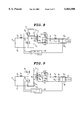
FIGS. 1 and 2 of the accompanying drawings show conventional switching power supplies. The conventional switching power supply shown in FIG. 1 is of the general forward type. For making a highly efficient switching power supply, particularly a switching power supply with a low-voltage (e.g., 5 V or 3.3 V), high-current output capability, using the circuit shown in FIG. 1, since rectifying diodes D101, D102 connected to the secondary winding N12 of a transformer T101 cause a large power loss, it is often customary to employ synchronous rectifying MOSFETs in place of the rectifying diodes D101, D102. It is of importance to consider how these synchronous rectifying MOSFETs (also referred to as synchronous rectifying transistors) are to be driven to achieve a highly efficient switching power supply.
The conventional switching power supply shown in FIG. 2 employs synchronous rectifying transistors Q102, Q103 instead of the rectifying diodes.
The conventional switching power supply shown in FIG. 1 which employs the rectifying diodes suffers the same problems as those of the conventional switching power supply shown in FIG. 2 which employs the synchronous rectifying transistors, except that the synchronous rectifying transistors are driven in the conventional switching power supply shown in FIG. 2. Therefore, the conventional switching power supply shown in FIG. 2 will be described below.
FIG. 3 of the accompanying drawings shows the waveforms of voltages and currents in various parts of the conventional switching power supply shown in FIG. 2. FIG. 4 of the accompanying drawings shows an output voltage of the conventional switching power supply shown in FIG. 2 with respect to a duty cycle (the ratio of an on-time to an operating period of a switching element Q101) thereof.
In FIG. 3, T1 represents an operating period of the switching element Q101, TON1 represents an on-time thereof, and Toff1, Toff2 represent an off-time thereof.
Vgs (Q101), Id (Q101), and Vds (Q101) represent agate voltage, a drain current, and a drain-to-source voltage, respectively, of the switching element Q101, and V(N11) represents a voltage across the primary winding N11 of the transformer T101.
Of the voltage V(N11) across the primary winding of the transformer T101, a voltage V(1) in the off-time Toff1 of the switching element Q101 is generated to reset the transformer T101, after it has been excited in the on-time TON1 of the switching element Q101. The voltage V(h1) is generated such that an integral of the voltage with respect to time in the on-time will be equal to an integral of the voltage with respect to time in the off-time.
The waveform of the voltage V(N11) in the off-time Toff1 is determined depending on the magnetizing inductance and the capacitance between output terminals of the switching element Q101. When the voltage of an input power supply Vin and an output current supplied to a load vary, the duty cycle of the switching element Q101 varies to keep the output voltage constant, and the voltage V(h1) and the off-times Toff1, Toff2 also vary.
In order to reset the transformer T101 in the off-time Toff1 by exactly the same quantity as it has been excited in the on-time TON1 under any input and output conditions, it is necessary to sufficiently provide the off-time Toff2 in which no voltage is induced across the primary winding N11, after the resetting of the transformer T101. As described later on, the need to increase the off-time Toff2 poses a serious problem.
In FIG. 3, Vds (Q102) represents a drain-to-source voltage of the synchronous rectifying transistor Q102 , and Vds (Q103) represents a drain-to-source voltage of the synchronous rectifying transistor Q103. These voltages are voltages converted from the voltage V(N11), in the respective off-and on-times Toff1, TON1, across the primary winding N11 of the transformer T101 with the turns ratio of the primary and secondary windings N11, N12 of the transformer T101.
One major problem encountered in making a highly efficient switching power supply using the circuit shown in FIG. 2 is that since the drain-to-source voltage Vds (Q102) of the synchronous rectifying transistor Q102 is large as shown in FIG. 3, the synchronous rectifying transistor Q102 has a large on-state resistance and causes a large power loss, resulting in a reduction in the switching power supply efficiency.
Specifically, though the synchronous rectifying transistor Q102 should have a smaller on-state resistance for higher switching power supply efficiency, MOSFETs have such a general tendency that their on-state resistance is higher as the drain-source breakdown voltage is higher.
The voltage V(N11) in the off-time Toff1 across the primary winding N11 of the transformer T101 is of a sine wave because it resonates with the magnetizing inductance and the capacitance between the drain and source of the switching element Q101, and hence has a large maximum level. Furthermore, since the voltage V(N11) varies greatly depending on the input and output conditions, the synchronous rectifying transistor Q102 is required to have a large dielectric strength between the drain and source thereof and hence a large on-state resistance.
The above problem holds true for the conventional switching power supply shown in FIG. 1 where the rectifying diode D101, is used in place of the synchronous rectifying transistor Q102.
The problem of the dielectric strength of the synchronous rectifying transistor Q102 is also the problem of the dielectric strength of the switching element Q101. One conventional way of limiting the dielectric strength to a certain voltage is to use a clamping circuit, which comprises a diode, a capacitor, and a resistor, between the terminals of the primary winding N11 of the transformer T101. Though the clamping circuit is capable of clamping the voltage to a certain level, however, the efficiency is lowered because the magnetization energy of the transformer T101 is consumed by the resistance of the clamping circuit. According to another conventional way of clamping the voltage, a tertiary winding is added to the transformer T101, and connected to the input power supply Vin via a diode, thus providing a clamping circuit.
With the latter conventional clamping circuit, most of the excitation energy of the transformer T101 flows to the input power supply Vin. When this current flows through the diode of the clamping circuit, the diode develops a voltage drop which causes a power consumption resulting in a reduction in the efficiency. In addition, the transformer T101 is large in size and complex in structure because of the added tertiary winding, and the tertiary winding suffers an increased conduction loss.
Another drawback which results from making a highly efficient switching power supply using the circuit shown in FIG. 2 is that because of the off-time Toff2 shown in FIG. 3, the synchronous rectifying transistor Q103 cannot be energized for the entire period in which the switching element Q101 is turned off, resulting in a reduction in the switching power supply efficiency. This drawback is inherent in using synchronous rectifying transistors, and is the most serious in the manufacture of highly efficient switching power supplies. In the on-time TON1 of the switching element Q101, the synchronous rectifying transistor Q103 is turned off and the synchronous rectifying transistor Q102 is turned on, and a current through a choke coil L10 flows through the synchronous rectifying transistor Q102. In the off-time Toff1 of the switching element Q101, the synchronous rectifying transistor Q102 is turned off and the synchronous rectifying transistor Q103 is turned on, and a current through a choke coil L10 flows through the synchronous rectifying transistor Q103.
The gate terminals of the synchronous rectifying transistors Q102, Q103 are energized by the voltage across the secondary winding N12 of the transformer T101. When one of the synchronous rectifying transistors Q102, Q103 is turned on, the gate voltage thereof comes from the drain-to-source voltage of the other synchronous rectifying transistor which is turned off.
The switching element Q101 has the off-times Toff1, Toff2. As can be seen from FIG. 3, since the drain-to-source voltage Vds (Q102) of the synchronous rectifying transistor Q102 has a certain level in the off-time Toff1, the synchronous rectifying transistor Q103 can be energized in the off-time Toff1. However, in the off-time Toff2, the synchronous rectifying transistor Q103 cannot be energized because the drain-to-source voltage Vds (Q102) is nil. Therefore, the synchronous rectifying transistor Q103 is turned off in the off-time Toff2. During this time, a current through the choke coil L10 flows through a body diode of the synchronous rectifying transistor Q103, i.e., a parasitic diode inserted from the source terminal to the drain terminal thereof because of the MOSFET structure. Inasmuch as a voltage drop across the body diode is much greater than a voltage drop caused when the synchronous rectifying transistor Q103 is turned on, the power loss in the off-time Toff2 is increased, reducing the switching power supply efficiency.
Still another shortcoming is that the choke coil of the output filter is large because an output ripple voltage is high. Stated otherwise, if a chock coil of a certain size is used to keep the output ripple voltage to a prescribed level, then the iron loss and copper loss of the chock coil are increased, indirectly lowering the efficiency of the switching power supply.
In FIG. 3, the drain-to-source voltage Vds (Q103) of the synchronous rectifying transistor Q103 is the same as a voltage V(P) at a point P shown in FIG. 2. The voltage V(P) is averaged by an output filter, which comprises the choke coil L10 and a capacitor C10, into an output voltage Vout free of alternating current components. The output voltage Vout is indicated in relation to the drain-to-source voltage Vds (Q103) in FIG. 3. The drain-to-source voltage Vds (Q103) and the output voltage Vout across the capacitor C10 are applied respectively to the terminals of the choke coil L10. The difference between the drain-to-source voltage Vds (Q103) and the output voltage Vout determines a ripple current I(L10) flowing through the choke coil L10. The product of the ripple current I(L10) and the equivalent series resistance of the capacitor C10 approximately determines the value of an output ripple voltage.
FIG. 4 shows an output voltage of the conventional switching power supply shown in FIG. 2 with respect to a duty cycle thereof, as described above. As can be understood from FIG. 4, since the output voltage is proportional to the duty cycle, the duty cycle is set to nearly 0.5 generally when the input and output conditions are rated conditions. According to the waveform of the drain-to-source voltage Vds (Q103), the ratio of the period in which the drain-to-source voltage Vds (Q103) is nil, i.e., the sum of the off-times Toff1, Toff2, to the entire time, i.e., the operating period T1, is about 50%, so that the output ripple voltage is large. Stated otherwise, if a chock coil of a certain size is used to keep the output ripple voltage to a prescribed level, then the iron loss and copper loss of the chock coil are increased, indirectly lowering the efficiency of the switching power supply.
As described above, when a highly efficient switching power supply is to be constructed using the circuit shown in FIG. 2, the rectifying elements of the rectifying circuit connected to the secondary winding of the transformer cause a large power loss, and it is important to consider how the power loss can be reduced. Recently, efforts have been made to use synchronous rectifying transistors in place of the rectifying elements for there by reducing their conduction loss. It is also important to pay attention to effective energization of the synchronous rectifying transistors.
SUMMARY OF THE INVENTION
It is an object of the present invention to provide a switching power supply which employs rectifying elements of low dielectric strength that suffer a relatively small power loss, and allows synchronous rectifying transistors used as such rectifying elements to be energized for an entire period, so that the switching power supply can operate highly efficiently.
According to an aspect of the present invention, there is provided a power supply circuit comprising first and second choke coils, first and second capacitors, first and second switching elements each comprising a MOSFET, first and second synchronous rectifying transistors each comprising a MOSFET, a transformer having a primary winding and first and second secondary windings which are magnetically coupled to the primary winding, the first and second switching elements being connected in series with each other at a junction, jointly making up a series-connected circuit, the primary winding and the first choke coil having respective terminals connected to the junction between the first and second switching elements, the first and second capacitors being connected in series with each other at a junction, jointly making up a series-connected circuit, the primary winding having another terminal connected to the junction between the first and second capacitors, the series-connected circuit of the first and second switching elements and the series-connected circuit of the first and second capacitors being connected parallel to each other, jointly making up a parallel-connected circuit, and a power supply for applying a voltage between a terminal of the parallel-connected circuit and another terminal of the first choke coil, the arrangement being such that when the first and second switching elements are alternately turned on, an alternating current flows through the primary winding to induce alternating-current voltages respectively across the first and second secondary windings for thereby alternately turning on the first and second synchronous rectifying transistors to cause a current to flow alternatively through the first and second secondary windings for supplying a current to the second choke coil.
According to another aspect of the present invention, there is also provided a power supply circuit comprising first and second choke coils, first and second capacitors, first and second switching elements each comprising a MOSFET, first and second synchronous rectifying transistors each comprising a MOSFET, a transformer having a primary winding and first and second secondary windings which are magnetically coupled to the primary winding, the first and second switching elements being connected in series with each other at a junction, jointly making up a series-connected circuit, the primary winding and the first choke coil having respective terminals connected to the junction between the first and second switching elements, the second capacitor being connected parallel to the series-connected circuit of the first and second switching elements, jointly making up a parallel-connected circuit, the parallel-connected circuit having a terminal connected by the first capacitor to another terminal of the primary winding, and a power supply for applying a voltage between a junction between the parallel-connected circuit and the first capacitor, and another terminal of the first choke coil, the arrangement being such that when the first and second switching elements are alternately turned on, an alternating current flows through the primary winding to induce alternating-current voltages respectively across the first and second secondary windings for thereby alternately turning on the first and second synchronous rectifying transistors to cause a current to flow alternatively through the first and second secondary windings for supplying a current to the second choke coil.
According to still another aspect of the present invention, there is further provided a power supply circuit comprising first and second choke coils, first and second capacitors, first and second switching elements each comprising a MOSFET, first and second synchronous rectifying transistors each comprising a MOSFET, a transformer having a primary winding, first and second secondary windings which are magnetically coupled to the primary winding, and a tertiary winding which is magnetically coupled to the primary winding and the first and second secondary windings, the primary winding and the first capacitor being connected in series with each other, jointly making up a series-connected circuit, the first switching element being connected parallel to the series-connected circuit of the primary winding and the first capacitor, jointly making up a parallel-connected circuit, the parallel-connected circuit having a terminal connected to a terminal of the first choke coil, and a power supply for applying a voltage between another terminal of the parallel-connected circuit and another terminal of the first choke coil, the tertiary winding and the second capacitor being connected in series with each other, jointly making up a series-connected circuit, the second switching element being connected parallel to the series-connected circuit of the tertiary winding and the second capacitor, the arrangement being such that when the first and second switching elements are alternately turned on, an alternating current flows through the primary winding to induce alternating-current voltages respectively across the first and second secondary windings for thereby alternately turning on the first and second synchronous rectifying transistors to cause a current to flow alternatively through the first and second secondary windings for supplying a current to the second choke coil.
In each of the above power supply circuits, the first and second secondary windings have respective terminals connected to each other at a junction, the second choke coil having a terminal connected to the junction between the first and second secondary windings, and the first and second secondary windings have respective other terminals connected to each other by the first or second synchronous rectifying transistor at a junction, with an output voltage being extracted between the junction between the other terminals of the first and second secondary windings and another terminal of the second choke coil, the arrangement being such that a voltage at the other terminal of the second secondary winding is applied to a gate terminal of one of the first and second synchronous rectifying transistors which is connected to the first secondary winding, and a voltage at the other terminal of the first secondary winding is applied to a gate terminal of one of the first and second synchronous rectifying transistors which is connected to the second secondary winding.
Either one of the first and second switching elements is turned on for an on-time except for a relatively short off-time in which both of the first and second switching elements are prevented from being turned on at the same time, the on-time being variable to keep constant the output voltage extracted from the second choke coil.
The power supply circuit further comprises an output capacitor for smoothing the output voltage.
The above and other objects, features, and advantages of the present invention will become more apparent from the following description when taken in conjunction with the accompanying drawings in which preferred embodiments of the present invention are shown by way of illustrative example.
BRIEF DESCRIPTION OF THE DRAWINGS
FIG. 1 is a circuit diagram of a conventional switching power supply;
FIG. 2 is a circuit diagram of another conventional switching power supply;
FIG. 3 is a diagram showing the waveforms of voltages and currents in various parts of the conventional switching power supply shown in FIG. 2;
FIG. 4 is a diagram showing an output voltage of the conventional switching power supply shown in FIG. 2 with respect to a duty cycle (the ratio of on-time to operating period of a switching element Q101) thereof;
FIG. 5 is a circuit diagram of a switching power supply according to a first embodiment of the present invention;
FIG. 6 is a circuit diagram showing a current path in the switching power supply according to the first embodiment of the present invention;
FIG. 7 is a circuit diagram showing another current path in the switching power supply according to the first embodiment of the present invention;
FIG. 8 is a circuit diagram showing other current paths in the switching power supply according to the first embodiment of the present invention;
FIG. 9 is a circuit diagram showing other current paths in the switching power supply according to the first embodiment of the present invention;
FIG. 10 is a diagram showing the waveforms of voltages and currents in various parts of the switching power supply according to the first embodiment of the present invention;
FIG. 11 is a diagram showing an output voltage of the switching power supply according to the first embodiment of the present invention with respect to a duty cycle (the ratio of on-time to operating period of a switching element Q1) thereof;
FIGS. 12a through 12c are circuit diagrams illustrative of the manner in which the switching power supply according to the first embodiment of the present invention operates;
FIG. 13 is a circuit diagram illustrative of another process of driving synchronous rectifying MOSFETs;
FIG. 14 is a circuit diagram of a switching power supply according to a second embodiment of the present invention;
FIGS. 15a and 15b are circuit diagrams illustrative of the manner in which the switching power supply according to the second embodiment of the present invention operates;
FIG. 16 is a circuit diagram of a switching power supply according to a third embodiment of the present invention;
FIG. 17 is a circuit diagram showing a current path in the switching power supply according to the third embodiment of the present invention;
FIG. 18 is a circuit diagram showing current paths in the switching power supply according to the third embodiment of the present invention; and
FIG. 19 is a circuit diagram showing current paths in the switching power supply according to the third embodiment of the present invention.
DETAILED DESCRIPTION OF THE PREFERRED EMBODIMENTS
As shown in FIG. 5, a switching power supply according to a first embodiment of the present invention has an input power supply Vin, a pair of input terminals 2a, 2b, a first choke coil L1, a pair of first and second switching elements Q1, Q2, a pair of first and second capacitors C1, C2, a transformer T having a primary winding N1 and a pair of first and second secondary windings Na, Nb, a pair of first and second synchronous rectifying transistors Q3, Q4, an output filter comprising a second choke coil L2 and an output capacitor Cout, a pair of output terminals 16a, 16b, a load 17, and a control circuit 18.
The parts connected to the primary winding N1 of the transformer T will be described in detail below.
The input power supply Vin has a positive terminal connected to the input terminal 2a and a negative terminal connected to the input terminal 2b which is kept at ground potential.
Each of the first and second switching elements Q1, Q2 comprises an n-channel MOSFET. The first switching element Q1 has a drain terminal connected to the source terminal of the second switching element Q2 and a source terminal connected to ground. The first and second switching elements Q1, Q2 jointly make up a series-connected circuit 41. Diodes which are shown connected respectively across the first and second switching elements Q1, Q2 are parasitic diodes in their MOSFETS.
The first and second capacitors C1, C2 are connected in series with other and jointly make up a series-connected circuit 42 which has a terminal connected to the drain terminal of the second switching element Q2 and an opposite terminal connected to ground. The series-connected circuit 42 is connected parallel to the series-connected circuit 41, jointly making up a parallel-connected circuit 43.
The first choke coil L1 has a terminal connected to the input terminal 2a connected to the positive terminal of the input power supply Vin. The other terminal of the first choke coil L1 is connected to the junction between the first and second switching elements Q1, Q2.
The junction between the first and second switching elements Q1, Q2 is connected to a terminal of the primary winding N1 of the transformer T. The other terminal of the primary winding N1 is connected to the junction between the first and second capacitors C1, C2.
The parts connected to the first and second secondary windings Na, Nb of the transformer T will be described in detail below. Each of the first and second synchronous rectifying transistors Q3, Q4 comprises an n-channel MOSFET. The first and second secondary windings Na, Nb have terminals connected to each other and other terminals connected to the gate terminals of the first and second synchronous rectifying transistors Q3, Q4. The junction between the first secondary winding Na and the gate terminal of the first synchronous rectifying transistor Q3 is connected to the drain terminal of the second synchronous rectifying transistor Q4. Similarly, the junction between the second secondary winding Nb and the gate terminal of the second synchronous rectifying transistor Q4 is connected to the drain terminal of the first synchronous rectifying transistor Q3.
The first and second synchronous rectifying transistors Q3, Q4 have respective source terminals connected to each other, and the output terminal 16b which is held at ground potential is connected to the junction between the source terminals of the first and second synchronous rectifying transistors Q3, Q4.
The first and second secondary windings Na, Nb are magnetically coupled to the primary winding N1 of the transformer T. The terminal of the primary winding N1 which is connected to the first and second switching elements Q1, Q2 is of the same polarity as that of the terminal of the first secondary winding Na which is connected to the second synchronous rectifying transistor Q4, and also of the same polarity as that of the terminal of the second secondary winding Nb which is connected to the first secondary winding Na.
The junction between the first and second secondary windings Na, Nb is connected to a terminal of the second choke coil L2, whose other terminal is connected to the output terminal 16a which is kept at a positive potential.
The output capacitor Cout is connected between the output terminals 16a, 16b. The load 17 is also connected between the output terminals 16a, 16b parallel to the output capacitor Cout.
After a voltage from the input power supply Vin is applied, when the first switching element Q1 is turned on with the second switching element Q2 being turned off, a current flows along a path indicated by J1 in FIG. 6, storing energy in the first choke coil L1.
Then, when the first switching element Q1 is turned off and the second switching element Q2 is turned on, an electromotive force is induced across the choke coil L1 by the energy stored in the choke coil L1, rendering the second switching element Q2 conductive in the reverse direction. A current flows in a path indicated by J2 in FIG. 7 from the source terminal to the drain terminal of the second switching element Q2, charging the first and second capacitors C1, C2.
The state in which the first and second capacitors C1, C2 are charged is referred to as a steady state. When the first switching element Q1 is turned off and the second switching element Q2 is turned on in the steady state, the second capacitor C2 is discharged, causing a current to flow from the drain terminal of the second switching element Q2 to the source terminal thereof to the primary winding N1 along a path indicated by J3 in FIG. 8.
When the first switching element Q1 is turned on and the second switching element Q2 is turned off in the steady state, the first capacitor C1 is discharged, causing a current to flow from the drain terminal of the first switching element Q1 to the source terminal thereof to the primary winding N1 along a path indicated by J4 in FIG. 9. At this time, the current flows through the primary winding N1 in the direction opposite to the direction in which it flows when the second switching element Q2 is turned on.
Operation of the switching power supply shown in FIG. 5 in the steady state will be described below with reference to FIG. 10.
In FIG. 10, T31 represents an operating period of the switching elements, TON31 represents an on-time of the first switching element Q1, TON32 represents an on-time of the second switching element Q2, and Toff31, Toff32 represent off-times in which both the first and second switching elements Q1, Q2 are turned off. The off-times Toff31, Toff32 are a period in which both the first and second switching elements Q1, Q2 are prevented from being turned on at the same time, so that series-connected circuit of the first and second capacitors C1, C2 is prevented from being short-circuited. The off-times Toff31, Toff32 may be of a minimum required period in view of delay times of the first and second switching elements Q1, Q2 upon switching thereof.
In FIG. 10, Vgs (Q1), Vgs (Q2) represent gate drive voltages of the first and second switching elements Q1, Q2, respectively.
It can be seen from FIG. 10 that the first and second switching elements Q1, Q2 are controlled by the control circuit 18 such that when one of the first and second switching elements Q1, Q2 is turned on, the other is turned off, and vice versa except for the short off-times Toff31, Toff32, and that the ratio of the on-time of one of the first and second switching elements Q1, Q2 to the operating period T31, i.e., the duty cycle, is varied to produce a constant output voltage Vout.
In FIG. 10, I(L1) represents a current flowing through the first choke coil L1, I(N1) and V(N1) represent a current flowing through and a voltage developed across the primary winding N1 of the transformer T, respectively, I(Q1) and I(Q2) represent currents flowing through the first and second switching elements Q1, Q2, respectively, Vds (Q3), Vds (Q4) represent drain-to-source voltages of the first and second synchronous rectifying transistors Q3, Q4, respectively, V(R) represents a voltage at the junction (point R in FIG. 5) between the first and second secondary windings Na, Nb of the transformer T, and I(L2) represents a current flowing through the second choke coil L2.
Prior to describing the waveforms of voltages and currents shown in FIG. 10, operation in the steady state of the switching power supply shown in FIG. 5 will be described below with reference to FIGS. 12a, 12b, and 12c.
Operation of the switching power supply shown in FIG. 5 may be considered as a combination of operation of the circuits shown in FIGS. 12a, 12b. In the switching power supply shown in FIG. 5, the second switching element Q2 is turned off in the on-time of the first switching element Q1, and turned on in the off-time of the first switching element Q1. Therefore, the second switching element Q2 operates in the same manner as a commutating diode D21 in a booster chopper circuit shown in FIG. 12c. Therefore, the circuit shown in FIG. 12a may be replaced with the circuit shown in FIG. 12c, and hence may be regarded as a booster chopper circuit.
Since the series-connected circuit of the first and second capacitors C1, C2 shown in FIG. 12b is charged to the single polarity as described above with reference to FIG. 7, it is possible for the first and second capacitors C1, C2 to maintain a certain DC voltage if the first and second capacitors C1, C2 have a sufficiently large capacitance. Consequently, the series-connected circuit of the first and second switching elements Q1, Q2 may be considered as a half-bridge circuit with the series-connected circuit of the first and second capacitors C1, C2 serving as its input power supply.
The operation of the switching power supply shown in FIG. 5 may be considered as a combination of the operation of the booster chopper circuit shown in FIG. 12a in which the input power supply Vin supplies electric energy to the series-connected circuit of the first and second capacitors C1, C2 and the operation of the half-bridge circuit shown in FIG. 12b in which the series-connected circuit of the first and second capacitors C1, C2 supplies electric energy to the load 17 (a quantitative analysis of the above operation will be described later on).
The first and second capacitors C1, C2 operate with a certain DC voltage because of the operation of the booster chopper circuit shown in FIG. 12a. In the half-bridge circuit shown in FIG. 12b, the ratio of the on-time of one of the first switching element Q1 to the operating period T31 is varied.
The waveforms of voltages and currents shown in FIG. 10 will be described in detail below.
In the on-time TON31 of the first switching element Q1, the current I(L1) flows from the input power supply Vin through the first choke coil L1 to the first switching element Q1. At this time, the current I(L1) flows along the path indicated by J1 in FIG. 6, and has a waveform those gradient is indicated by Va /La where Va represents the voltage of the input power supply Vin and La represents the inductance of the first choke coil L1.
When the first capacitor C1 is discharged, the current I(N1) flows from the positive-voltage terminal of the first capacitor C1 through the primary winding N1 of the transformer T and the first switching element Q1 back to the negative-voltage terminal (ground terminal) of the first capacitor C1, along the path indicated by J4 in FIG. 9. When the current I(N1) flows through the primary winding N1, it induces a voltage across the second secondary winding Nb, turning on the second synchronous rectifying transistor Q4. A voltage is then induced across the first secondary winding Na, causing a current to flow along a path indicated by J6 in FIG. 9. The current supplies electric energy to the load 17, and charges the output capacitor Cout. It is assumed that at this time the current flows through the primary winding N1 in a positive direction.
The current flowing through the primary winding N1 is equal to the sum of a current converted from the current flowing through the second choke current L2 with the turns ratio of the transformer T and an magnetizing current of the transformer T.
As described above, the current which is equal to the sum of the current flowing through the first choke coil L1 along the path indicated by J1 in FIG. 6 and the current flowing through the primary winding N1 along the path indicated by J4 in FIG. 9 flows through the first switching element Q1. This current has a waveform I(Q1) as shown in FIG. 10.
In the on-time TON32 in which the first switching element Q1 is turned off and the second switching element Q2 is turned on, the current I (L1) flows through the first choke coil L1. The current I(L1) is generated by an electromotive force induced across the first choke coil L1, and flows from the positive-voltage terminal of the first choke coil L1 through the second switching element Q2, the second capacitor C2, the first capacitor C1, and the input power supply Vin back to the negative-voltage terminal of the first choke coil L1, along the path indicated by J2 in FIG. 7, charging the series-connected circuit of the first and second capacitors C1, C2. This current corresponds to the current flowing through the first choke coil L1 and the diode D21 with the first switching element Q1 being turned off, in the booster chopper circuit shown in FIG. 12c.
The current has a wavef orm whose gradient is indicated by (Va -Vb)/La where Va represents the voltage of the input power supply Vin, La represents the inductance of the first choke coil L1, and Vb represents the voltage across the series-connected circuit of the first and second capacitors C1, C2.
In the on-time TON32 of the second switching element Q2, the second capacitor C2 is discharged, causing the current I(N1) to flow through the primary winding N1 of the transformer T, along the path indicated by J3 in FIG. 8. This current flows from the positive-voltage terminal of the second capacitor C2 through the second switching element Q2 and the primary winding N1 back to the negative-voltage terminal of the second capacitor C2.
At this time, the current flowing through the primary winding N1 is equal to the sum of a current converted from the current flowing through the second choke current L2 with the turns ratio of the transformer T and an magnetizing current of the transformer T.
Since the current flows through the primary winding N1 along the path indicated by J3 in FIG. 8, a positive voltage is applied to the gate terminal of the first synchronous rectifying transistor Q3 by an electromotive force induced across the first secondary winding Na, thus turning on the first synchronous rectifying transistor Q3.
As a result, due to the electromotive force developed across the second secondary winding Nb, a current flows along a path indicated by J5 in FIG. 8, supplying electric energy to the load 17 and charging the output capacitor Cout.
In the on-time TON32 of the second switching element Q2, the electromotive force developed across the first choke coil L1 causes a current to flow through the second switching element Q2 in the direction to charge the first and second capacitors C1, C2 along the path indicated by J2 in FIG. 7.
Therefore, in the on-time TON32 of the second switching element Q2, the current flows from the drain terminal to the source terminal of the second switching element Q2 along the path indicated by J3 in FIG. 8 because of the discharging of the second capacitor C2, and the current flows from the source terminal to the drain terminal of the second switching element Q2 along the path indicated by J2 in FIG. 7 because of the electromotive force developed across the first choke coil L1.
As a consequence, a current which is the difference between the current I(L1) flowing through the first choke coil L1 and the current I(N1) flowing through the primary winding N1 of the transformer T flows through the second switching element Q2. This current has a waveform indicated by I(Q2) in FIG. 10.
In FIG. 10, V(N1) represents a voltage developed across the primary winding N1 of the transformer T. This voltage in the on-time TON31 corresponds to the voltage across the first capacitor C1 because the first switching element Q1 is turned on, and in the on-time TON32 corresponds to the voltage across the second capacitor C2 because the second switching element Q2 is turned on.
In FIG. 10, Vds (Q3), Vds (Q4) represent, respectively, drain-to-source voltages of the first and second synchronous rectifying transistors Q3, Q4 in FIG. 5. These drain-to-source voltages serve as respective gate drive voltages of the second and first synchronous rectifying transistors Q4, Q3.
In FIG. 10, V(R) represents a voltage at the point R in FIG. 5 between the first and second secondary windings Na, Nb of the transformer T, and I(L2) represents a current flowing through the second choke coil L2.
The drain-to-source voltages Vds (Q3), Vds (Q4) are voltages converted from the voltage V(N1) across the primary winding N1 respectively in the on-times TON31, TON32 with the turns ratio between the primary winding N1 and the first secondary winding Na (or the second secondary winding Nb). The voltage V(R) at the point R is equal to the sum of the drain-to-source voltages Vds (Q3), Vds (Q4).
Of the voltage V(R), Vout represents the output voltage between the output terminals 16a, 16b. The voltage V(R) at the point R and the output voltage Vout are applied across the second choke coil L2, causing a ripple current I(L2) to flow through the second choke coil L2. A ripple voltage whose value is substantially determined by the product of the ripple current I(L2) and an equivalent series resistance of the output capacitor Cout is generated in the output voltage.
As can be seen from the above description, according to the first embodiment shown in FIG. 5, either one of the drain-to-source voltages Vds (Q3), Vds (Q4) of the first and second synchronous rectifying transistors Q3, Q4 is generated at all times except for the short off-times Toff31, Toff32.
Therefore, when a voltage is induced across the first secondary winding Na or the second secondary winding Nb, applying a higher voltage to the source terminal of the second synchronous rectifying transistor Q4 or the second synchronous rectifying transistor Q3 than to the drain terminal thereof, a positive voltage is applied to the gate terminal of the synchronous rectifying transistor, turning on the synchronous rectifying transistor. Therefore, the synchronous rectifying transistor is prevented from being turned off, preventing a current from flowing from the source terminal to the drain terminal thereof through the internal parasitic diode, so that no large loss will be caused. The switching power supply according to the present invention is therefore free of "the problem of a large loss because of a long period of time in which the synchronous rectifying transistor could not be energized."
As can be understood from the waveforms of the drain-to-source voltages Vds (Q3), Vds (Q4), since the voltages applied to the first and second synchronous rectifying transistors Q3, Q4 are of rectangular waveforms, these voltages are prevented from being unduly increased whereas they posed a problem in the conventional circuit arrangement because they are of a resonating waveform. The switching power supply according to the present invention may thus employ synchronous rectifying transistors having a low dielectric strength and a low on-state resistance.
An output voltage of the switching power supply shown in FIG. 5 with respect to a duty cycle (the ratio of the on-time to the operating period of the switching element Q1) thereof will be described with reference to FIG. 11.
It is assumed that the voltage of the input power supply Vin is represented by Va, the duty cycles of the respective first and second switching elements Q1, Q2 are represented by D, 1-D, respectively, the voltages across the first and second capacitors C1, C2 are represented by V(C1), V(C2), respectively, the turns ratio between the primary winding N1 and the first secondary winding Na (or the second secondary winding Nb) is represented by n: 1, the drain-to-source voltages of the first and second synchronous rectifying transistors Q3, Q4 are represented by Vds (Q3), Vds (Q4), respectively, and the output voltage between the output terminals 16a, 16b is represented by Vout. From the circuit arrangement of the booster chopper circuit shown in FIG. 12a, the following equation (1) is satisfied (it is also assumed that, in the following numerical analysis, voltage drops developed across the first and second switching elements Q1, Q2 and the first and second synchronous rectifying transistors Q3, Q4 when they are rendered conductive are negligibly small, and the off-times Toff31, Toff32 in which both the first and second switching elements Q1, Q2 are turned off are also negligibly small):
V(C.sub.1)+V(C.sub.2)=V.sub.a /(1-D)                       (1)
With respect to the operation of the core (magnetic material) of the transformer T, the quantity by which the core is excited in the on-time of the first switching element Q1 is equal to the quantity by which the core is reset in the on-time of the second switching element Q2. Therefore, the following equation (2) is satisfied:
V(C.sub.1)×D=V(C.sub.2)×(1-D)                  (2)
From the equations (1), (2), the following equations (3), (4) are derived:
V(C.sub.1)=V.sub.a                                         (3)
V(C.sub.2)=V.sub.a ×D/(1-D)                          (4)
Since the drain-to-source voltages of the first and second synchronous rectifying transistors Q3, Q4, at the time they are turned off are voltages converted from the voltages across the first and second capacitors C1, C2 with the turns ratio of the transformer T, the following equations (5), (6) are satisfied:
V.sub.ds (Q.sub.3)=V(C.sub.1)/n=V.sub.a /n                 (5)
V.sub.ds (Q.sub.4)=V(C.sub.2)/n=V.sub.a ×D/{(1-D)×n}(6)
The output voltage between the output terminals 16a, 16b is of a value produced by averaging the voltage at the point R with the output filter, and the voltage at the point R is equal to the sum of the drain-to-source voltages Vds (Q3), Vds (Q4) of the first and second synchronous rectifying transistors Q3, Q4. Therefore, if the switching period is represented by T0, then the following equation (7) is satisfied: ##EQU1##
From the equation (7), it can be seen that the output voltage Vout of the switching power supply shown in FIG. 5 is proportional to the duty cycle D of the switching element Q1, as shown in FIG. 11.
Since the output voltage Vout is proportional to the duty cycle D of the switching element Q1, as shown in FIG. 11, it is possible to set the duty cycle D to 0.5 provided the input and output conditions are rated conditions. At this time, both the drain-to-source voltages Vds (Q3), Vds (Q4) of the first and second synchronous rectifying transistors Q3, Q4 are represented by Va /n as can be understood from the equations (5), (6). Inasmuch as the drain-to-source voltages Vds (Q3), Vds (Q4) are variable about the value Va /n while keeping the rectangular waveform even when the input and output conditions are varied, the first and second synchronous rectifying transistors Q3, Q4 are not required to be of large dielectric strength and large on-state resistance unlike those of the conventional switching power supply.
The fact that the drain-to-source voltages Vds (Q3), Vds (Q4) are equal to each other (actually, they are slightly different from each other as the numbers of turns of the transformer T are integers) means that any changes in the voltage V(R) at the point R are very small. Because the voltage in the on-time TON31 and the voltage in the on-time TON32 are equal to each other or different from each other very slightly, the second choke coil L2 may be small, and any power loss caused by the second choke coil L2 may be small, so that the switching power supply may be highly efficient. Actually, the output filter is designed taking into account variations in the input and output conditions, but the second choke coil L2 may still be small.
The above analytical results have experimentally been verified.
In FIG. 10, I(N1) represents a current flowing through the primary winding N1 of the transformer T. Since the transformer T has a leakage inductance, the off-times Toff31, Toff31 in which both the first and second switching elements Q1, Q2 are turned off may be adjusted appropriately such that after one of the first and second switching elements Q1, Q2 is turned off and before the other of the first and second switching elements Q1, Q2 is turned on, a current due to the leakage inductance discharges the parasitic capacitor between the drain and source of the other switching element. As a result, the switching power supply can operate as a ZVS (Zero Voltage Switching) power supply.
Since the energy stored in the parasitic capacitor between the drain and source of the other switching element can be recovered, the efficiency of the switching power supply is increased.
As described above, with the switching power supply shown in FIG. 5, either one of the first and second synchronous rectifying transistors Q3, Q4 is energized at all times except for the short off-times Toff31, Toff32, i.e., the synchronous rectifying transistor through which the current flowing through the second choke coil L2 flows is energized, and their applied drain-to-source voltage is low. Therefore, the first and second synchronous rectifying transistors Q3, Q4 may be of small dielectric strength and small on-state resistance, and at the same time the output filter may be small and any power loss caused by the output filter may be small.
As a consequence, the switching power supply is highly efficient in operation.
In the switching power supply according to the second embodiment shown in FIG. 5, each of the first and second switching elements Q1, Q2 comprises an n-channel MOSFET. However, one or both of the first and second switching elements Q1, Q2 may comprise a p-channel MOSFET.
Furthermore, each of the first and second switching elements Q1, Q2 is not limited to a MOSFET, but may comprise an IGBT.
In the switching power supply shown in FIG. 5, since the first and second switching elements Q1, Q2 are symmetrically positioned, the series-connected circuit of the input power supply Vin and the first choke coil L1 may be connected between the drain and source of the second switching element Q2 rather than between the drain and source of the first switching element Q1. The switching power supply thus modified operates in the same manner as described above except that the first and second switching elements Q1, Q2 are switched around.
In the switching power supply shown in FIG. 5, the full-wave rectifier circuit comprising two rectifiers is connected to the secondary windings Na, Nb of the transformer T. However, a half-wave rectifier circuit with one of the two rectifiers used as a freewheeling rectifier may be connected to the secondary windings Na, Nb of the transformer T, or a full-wave rectifier circuit comprising a bridge of four rectifiers may be connected to the secondary windings Na, Nb of the transformer T.
A process of driving the first and second synchronous rectifying transistors Q3, Q4 in the switching power supply shown in FIG. 5 will be described below.
The gate terminal of each of the first and second synchronous rectifying transistors Q3, Q4 in the switching power supply shown in FIG. 5 is turned on by the drain-to-source voltage of the other first and second synchronous rectifying transistors Q3, Q4. However, the gate terminal of each of the first and second synchronous rectifying transistors Q3, Q4 may be turned on by a voltage obtained from the windings of the transformer T.
Another process of driving the first and second synchronous rectifying transistors Q3, Q4 is shown in FIG. 13. A switching power supply shown in FIG. 13 operates in a manner equivalent to the switching power supply shown in FIG. 5.
In the switching power supply according to the second embodiment shown in FIG. 14, the source terminal of a second switching element Q52 is connected to the drain terminal of the first switching element Q1, and the first and second switching element Q1, Q52 are connected in series with each other, thus jointly making up a series-connected circuit 44. A second capacitor C52 is connected parallel to the series-connected circuit 44, jointly making up a parallel-connected circuit 45.
The switching power supply shown in FIG. 14 is equivalent to the switching power supply shown in FIG. 5, and operates in the same manner as the switching power supply shown in FIG. 5. The switching power supply shown in FIG. 14 is equivalent to the switching power supply shown in FIG. 5 for the reasons which will be described below with reference to FIGS. 15a and 15b.
FIGS. 15a and 15b show half-bridge circuits which correspond to the switching power supplies according to the first and second embodiments, respectively. In FIG. 15a, the second switching element Q2 and the second capacitor C2 are connected in series with each other. In FIG. 15b, the second switching element Q52 and the second capacitor C52 are connected in series with each other. If the capacitor C52 shown in FIG. 15b has a capacitance equivalent to the combined capacitance of the series-connected capacitors C1, C2, then the capacitor C52 shown in FIG. 15b may be replaced with a capacitor C100 shown in FIG. 15b which has the same capacitance as the capacitance of the capacitor C2.
Therefore, the switching power supply shown in FIG. 14 offers the same advantages as those of the switching power supply according to the second embodiment shown in FIG. 5.
FIG. 16 shows a switching power supply according to a third embodiment of the present invention. In the switching power supply shown in FIG. 16, the first choke coil L1 has a terminal connected to the input terminal 2a which is connected to the positive-voltage terminal of the input power supply Vin. The other terminal of the first choke coil L1 is connected to a terminal of the primary winding N1 of a transformer T. The other terminal of the primary winding N1 is connected by the first capacitor C1 to the input terminal 2b which is kept at ground potential.
The primary winding N1 and the first capacitor C1 jointly make up a series-connected circuit 47. The first switching element Q1 which comprises an n-channel MOSFET is connected parallel to the series-connected circuit 47. The first switching element Q1 has a source terminal connected to ground and a drain terminal connected to the junction between the first choke coil L1 and the primary winding N1.
The parts connected to the first and second secondary windings Na, Nb of the transformer T are identical to those of the switching power supply according to the first embodiment. The first and second secondary windings Na, Nb are magnetically coupled to the primary winding N1 of the transformer T. The switching power supply shown in FIG. 16 additionally has a tertiary winding N3 magnetically coupled to the primary winding N1 and the first and second secondary windings Na, Nb.
The tertiary winding N3 has a terminal connected by a second capacitor C62 to the drain terminal of a second switching element Q62 which comprises an n-channel MOSFET. The other terminal of the tertiary winding N3 is connected to the source terminal of the second switching element Q62.
The tertiary winding N3 and the second capacitor C62 jointly make up a series-connected circuit 48. The second switching element Q62 is connected parallel to the series-connected circuit 48.
The terminal of the tertiary winding N3 which is connected to the second switching element Q62 is of the same polarity as that of the terminal of the primary winding N1 which is connected to the drain terminal of the first switching element Q1.
Operation of the switching power supply shown in FIG. 16 will be described below. After a voltage from the input power supply Vin is applied between the input terminals 2a, 2b, when the first switching element Q1 is turned on with the second switching element Q62 being turned off, electric energy is supplied from the input power supply Vin, causing a current to flow through the first choke coil L1 to the first switching element Q1 along a path indicated by J11 in FIG. 17.
When the first switching element Q1 is then turned off, a current flows along a path indicated by J12 in FIG. 18 due to an electromotive force developed across the first choke coil L1.
The current starts to flow from the terminal of the first choke coil L1 where a positive voltage is induced, and flows through the primary winding N1, thereby inducing voltages across the respective first and second secondary windings Na, Nb. The current flowing through the primary winding N1 flows into the first capacitor C1, thus charging first capacitor C1. The current thus passes through the input power supply Vin, and flows back to the terminal of the first choke coil L1 where a negative voltage is induced.
After the current has started to flow along the path indicated by J12 in FIG. 18 (at this time, the first switching element Q1 has changed from the on-state to the off-state), when the second switching element Q62 is turned on, a current flows from the source terminal to drain terminal of the second switching element Q62 along a path indicated by J14 in FIG. 18 due to an electromotive force developed across the tertiary winding N3, charging the second capacitor C62.
The first and second capacitors C1, C62 are thus charged when the first and second switching element Q1, Q62 are alternately rendered conductive.
The state in which the first and second capacitors C1, C62 are charged is referred to as a steady state. When the second switching element Q62 is rendered conductive with the second capacitor C62 being charged, a current flows along a path indicated by J15 in FIG. 18 due to the discharging of the second capacitor C62 at the same time that the current flows along the path indicated by J14 . The current flowing along the path indicated by J15 is opposite in direction to the current flowing along the path indicated by J14, and these current cancel out each other.
At this time, voltages are induced respective across the first and second secondary windings Na, Nb by the current flowing through the primary winding N1. The induced voltages are of such polarity that the second synchronous rectifying transistor Q4 is turned on, and a current flows from the terminal of the first secondary windings Na where a positive voltage is induced, through the second choke coil L2, the output capacitor Cout (or the load), the source terminal of the second synchronous rectifying transistor Q4, and the drain terminal thereof, to the terminal of the first secondary windings Na where a negative voltage is induced, along a path indicated by J13 in FIG. 18.
When the second switching element Q62 is turned off and the first switching element Q1 is turned on, a current is supplied from the input power supply Vin along the path indicated by J11 in FIG. 17, and the first capacitor C1 is discharged along a path indicated by J16 in FIG. 19.
Because of the discharging of the first capacitor C1, a current flows through the primary winding N1, turning on the first synchronous rectifying transistor Q3, and a current flows along a path indicated by J17 in FIG. 19.
When the first and second switching elements Q1, Q62 are thus alternately rendered conductive, the first and second synchronous rectifying transistors Q3, Q4 are also alternately rendered conductive, supplying electric energy to the output capacitor Cout and the load. While voltages are being induced across the first and second secondary windings Na, Nb, the first synchronous rectifying transistor Q3 or the second synchronous rectifying transistor Q4 is rendered conductive, with no current flowing through the internal parasitic diode. This operation is the same as the operation of the switching power supplies according to the first and second embodiments.
In the switching power supply according to the third embodiment shown in FIG. 16, voltages can be converted from the secondary side to the primary side of the transformer T with the turns ratio of the transformer T. The switching power supply according to the third embodiment has an equivalent circuit which is the same as the equivalent circuit of the switching power supply according to the first embodiment shown in FIG. 5. The switching power supply according to the third embodiment shown in FIG. 16 offers the same advantages as those of the switching power supply according to the first embodiment shown in FIG. 5.
According to the present invention, either one of the first and second synchronous rectifying transistors Q3, Q4 is energized at all times except for the short off-times Toff31, Toff32. Therefore, the first and second synchronous rectifying transistors Q3, Q4 may be of small dielectric strength and small on-state resistance, and at the same time the output filter may be small. Consequently, the switching power supply may be highly efficient in operation.
It is thus possible according to the present invention to make a highly efficient switching power supply with a low-voltage (e.g., 5 V or 3.3 V), high-current output capability for use in the field of communications or the like.
Although certain preferred embodiments of the present invention have been shown and described in detail, it should be understood that various changes and modifications may be made therein without departing from the scope of the appended claims.

Claims (6)

What is claimed is:
1. A power supply circuit comprising:
first and second choke coils;
first and second capacitors;
first and second switching elements each comprising a MOSFET;
first and second synchronous rectifying transistors each comprising a MOSFET;
a transformer having a primary winding and first and second secondary windings which are magnetically coupled to said primary winding;
said first and second switching elements being connected in series with each other at a junction, jointly making up a series-connected circuit, said primary winding and said first choke coil having respective terminals connected to said junction between the first and second switching elements;
said first and second capacitors being connected in series with each other at a junction, jointly making up a series-connected circuit, said primary winding having another terminal connected to said junction between the first and second capacitors;
said series-connected circuit of the first and second switching elements and said series-connected circuit of the first and second capacitors being connected parallel to each other, jointly making up a parallel-connected circuit; and
a power supply, operably connected to a terminal of said parallel-connected circuit and another terminal of said first choke coil, for applying a voltage between said terminal of said parallel-connected circuit and said another terminal of said first choke coil
wherein when said first and second switching elements are alternately tuned on, an alternating current flows through said primary winding to induce alternating-current voltages respectively across said first and second secondary windings for thereby alternately turning on said first and second synchronous rectifying transistors to cause a current to flow alternatively through said first and second secondary windings for supplying a current to said second choke coil.
2. A power supply circuit comprising:
first and second choke coils;
first and second capacitors;
first and second switching elements each comprising a MOSFET;
first and second synchronous rectifying transistors each comprising a MOSFET;
a transformer having a primary winding and first and second secondary windings which are magnetically coupled to said primary winding;
said first and second switching elements being connected in series with each other at a junction, jointly making up a series-connected circuit, said primary winding and said first choke coil having respective terminals connected to said junction between the first and second switching elements;
said second capacitor being connected parallel to said series-connected circuit of the first and second switching elements, jointly making up a parallel-connected circuit;
said parallel-connected circuit having a terminal connected by said first capacitor to another terminal of said primary winding; and
a power supply, operably connected to said parallel-connected circuit, said first capacitor, and another terminal of said first choke coil, for applying a voltage between a junction between said parallel-connected circuit and said first capacitor, and said another terminal of said first choke coil,
wherein when said first and second switching elements are alternately turned on, an alternating current flows through said primary winding to induce alternating-current voltages respectively across said first and second secondary windings for thereby alternately turning on said first and second synchronous rectifying transistors to cause a current to flow alternatively through said first and second secondary windings for supplying a current to said second choke coil.
3. A power supply circuit comprising:
first and second choke coils;
first and second capacitors;
first and second switching elements each comprising a MOSFET;
first and second synchronous rectifying transistors each comprising a MOSFET;
a transformer having a primary winding, first and second secondary windings which are magnetically coupled to said primary winding, and a tertiary winding which is magnetically coupled to said primary winding and said first and second secondary windings;
said primary winding and said first capacitor being connected in series with each other, jointly making up a series-connected circuit, said first switching element being connected parallel to said series-connected circuit of the primary winding and the first capacitor, jointly making up a parallel-connected circuit;
said parallel-connected circuit having a terminal connected to a terminal of said first choke coil; and
a power supply, operably connected to another terminal of said parallel-connected circuit and another terminal of said first choke coil, for applying a voltage between said another terminal of said parallel-connected circuit and said another terminal of said first choke coil;
said tertiary winding and said second capacitor being connected in series with each other, jointly making up a series-connected circuit, said second switching element being connected parallel to said series-connected circuit of the tertiary winding and the second capacitor,
wherein when said first and second switching elements are alternately turned on, an alternating current flows through said primary winding to induce alternating-current voltages respectively across said first and second secondary windings for thereby alternately turning on said first and second synchronous rectifying transistors to cause a current to flow alternately through said first and second secondary windings for supplying a current to said second choke coil.
4. A power supply circuit according to any one of claims 1 through 3, wherein said first and second secondary windings have respective terminals connected to each other at a junction, said second choke coil having a terminal connected to said junction between said first and second secondary windings, and wherein said first and second secondary windings have respective other terminals connected to each other by said first or second synchronous rectifying transistor at a junction, with an output voltage being extracted between the junction between the other terminals of the first and second secondary windings and another terminal of said second choke coil, the arrangement being such that a voltage at the other terminal of the second secondary winding is applied to a gate terminal of one of said first and second synchronous rectifying transistors which is connected to said first secondary winding, and a voltage at the other terminal of the first secondary winding is applied to a gate terminal of one of said first and second synchronous rectifying transistors which is connected to said second secondary winding.
5. A power supply circuit according to claim 4, wherein either one of said first and second switching elements is turned on for an on-time except for a relatively short off-time in which both of said first and second switching elements are prevented from being turned on at the same time, said on-time being variable to keep constant the output voltage extracted from said second choke coil.
6. A power supply circuit according to claim 5, further comprising an output capacitor for smoothing said output voltage.
US09/262,917 1998-03-09 1999-03-05 Switching power supply Expired - Lifetime US6064580A (en)

Applications Claiming Priority (2)

Application Number Priority Date Filing Date Title
JP07493098A JP3673075B2 (en) 1998-03-09 1998-03-09 Switching power supply
JP10-074930 1998-03-09

Publications (1)

Publication Number Publication Date
US6064580A true US6064580A (en) 2000-05-16

Family

ID=13561576

Family Applications (1)

Application Number Title Priority Date Filing Date
US09/262,917 Expired - Lifetime US6064580A (en) 1998-03-09 1999-03-05 Switching power supply

Country Status (6)

Country Link
US (1) US6064580A (en)
EP (1) EP0942519B1 (en)
JP (1) JP3673075B2 (en)
CA (1) CA2264443C (en)
DE (1) DE69901918T2 (en)
HK (1) HK1022218A1 (en)

Cited By (49)

* Cited by examiner, † Cited by third party
Publication number Priority date Publication date Assignee Title
US6188586B1 (en) * 2000-04-21 2001-02-13 Lucent Technologies Inc. Asymmetrical half-bridge power converter having reduced input ripple and method of manufacturing the same
US6198644B1 (en) * 1998-09-03 2001-03-06 Nagano Japan Radio Co., Ltd. Rectifying/smoothing circuit and double-ended converter
US6246598B1 (en) * 2000-08-02 2001-06-12 Polarity, Inc. High-voltage modulator system
US6288919B1 (en) * 1999-12-16 2001-09-11 Chippower.Com, Inc. Single stage AC/DC converter high frequency AC distribution systems
US6349044B1 (en) * 1999-09-09 2002-02-19 Virginia Tech Intellectual Properties, Inc. Zero voltage zero current three level dc-dc converter
US6353544B1 (en) * 2000-07-27 2002-03-05 Hua-In Co., Ltd. Flyback converter with synchronous rectifier
US20020122321A1 (en) * 2001-03-01 2002-09-05 Alain Chapuis Voltage converter
US6483722B2 (en) * 2000-11-10 2002-11-19 Fuji Electric Co., Ltd. DC/DC converter and control method thereof
US6483205B1 (en) * 2000-07-28 2002-11-19 Ricky Martin Distributed transformer control
US6545883B2 (en) * 2001-05-07 2003-04-08 Artesyn Technologies, Inc. Integrated boost-asymmetrical half-bridge converter
US20030086282A1 (en) * 2001-11-02 2003-05-08 Jianhong Zeng DC-to-DC converter
US6621722B1 (en) * 1998-12-07 2003-09-16 Lovoltech, Inc. Rectifier circuits with low forward voltage JFET device
US6650552B2 (en) * 2001-05-25 2003-11-18 Tdk Corporation Switching power supply unit with series connected converter circuits
US6696706B1 (en) 2002-10-22 2004-02-24 Lovoltech, Inc. Structure and method for a junction field effect transistor with reduced gate capacitance
US6734715B1 (en) 1999-11-29 2004-05-11 Lovoltech, Inc. Two terminal rectifier using normally off JFET
US20040145930A1 (en) * 2002-12-27 2004-07-29 Yamaha Corporation Power supply circuit
US6777722B1 (en) 2002-07-02 2004-08-17 Lovoltech, Inc. Method and structure for double dose gate in a JFET
US20040179378A1 (en) * 2003-03-11 2004-09-16 Denso Corporation Insulating switching DC/DC converter
US6807073B1 (en) 2001-05-02 2004-10-19 Oltronics, Inc. Switching type power converter circuit and method for use therein
US20050068792A1 (en) * 2003-09-30 2005-03-31 Masayuki Yasumura Switching power supply circuit
US6900506B1 (en) 2002-04-04 2005-05-31 Lovoltech, Inc. Method and structure for a high voltage junction field effect transistor
US6921932B1 (en) 2002-05-20 2005-07-26 Lovoltech, Inc. JFET and MESFET structures for low voltage, high current and high frequency applications
US20050237771A1 (en) * 2004-04-22 2005-10-27 Patent-Treuhand-Gesellschaft Fur Elektrisch Gluhlampen Mbh Circuit for converting an AC voltage to a DC voltage
US7038260B1 (en) 2003-03-04 2006-05-02 Lovoltech, Incorporated Dual gate structure for a FET and method for fabricating same
US7075132B1 (en) 2002-12-30 2006-07-11 Lovoltech, Inc. Programmable junction field effect transistor and method for programming the same
US20060226819A1 (en) * 2005-03-31 2006-10-12 Ming Xu Self-driven scheme for synchronous rectifier
US20070103005A1 (en) * 2005-11-08 2007-05-10 Toshio Nagasawa Switching power supply device, semiconductor integrated circuit device and power supply device
US7262461B1 (en) 2002-05-20 2007-08-28 Qspeed Semiconductor Inc. JFET and MESFET structures for low voltage, high current and high frequency applications
US7268378B1 (en) 2002-05-29 2007-09-11 Qspeed Semiconductor Inc. Structure for reduced gate capacitance in a JFET
US20070247123A1 (en) * 2006-04-19 2007-10-25 International Rectifier Corporation Single stage integrated boost inverter motor drive circuit
US20080049456A1 (en) * 2005-10-19 2008-02-28 Murata Manufacturing Co., Ltd. Synchronous rectifying forward converter
US20080049455A1 (en) * 2006-02-09 2008-02-28 Murata Manufacturing Co., Ltd. Forward converter with synchronous rectification
US20080285311A1 (en) * 2007-05-18 2008-11-20 Sanken Electric Co., Ltd. Dc-dc converter
US20090219006A1 (en) * 2008-02-28 2009-09-03 Fuji Electric Device Technology Co., Ltd. Electric power converter
US20100232189A1 (en) * 2009-03-13 2010-09-16 American Power Conversion Corporation Method for portioning output current of a dc-dc converter
US20110058396A1 (en) * 2006-01-19 2011-03-10 Conergy Ag Flyback-type inverter circuit for network supply or for network-independent operation
US20110188269A1 (en) * 2010-01-29 2011-08-04 Murata Manufacturing Co., Ltd. Switching power-supply apparatus
US20120033453A1 (en) * 2010-04-30 2012-02-09 Infineon Technologies Ag Controller for a Resonant Switched-Mode Power Converter
US20130294114A1 (en) * 2012-05-07 2013-11-07 Sanken Electric Co., Ltd. Direct-Current Converter
US20140268908A1 (en) * 2013-03-15 2014-09-18 Solarbridge Technologies, Inc. Converter topologies
CN104094378A (en) * 2012-02-29 2014-10-08 英福康有限责任公司 Device for supplying voltage to the cathode of a mass spectrometer
US20150043263A1 (en) * 2013-08-11 2015-02-12 Anatoly Diber Dc-ac inverter having controlled magnetization reversal of isolation transformer core
US20150333640A1 (en) * 2013-02-28 2015-11-19 Telefonaktiebolaget L M Ericsson (Publ) Forward-Flyback Topology Switched Mode Power Supply
US20160036337A1 (en) * 2013-05-21 2016-02-04 Murata Manufacturing Co Switching power supply apparatus
US9973073B2 (en) * 2016-08-24 2018-05-15 Omron Automotive Electronics Co., Ltd. Voltage conversion device that ensures supply of power to a controller even if the input voltage decreases
US20180191260A1 (en) * 2017-01-05 2018-07-05 Rohm Co., Ltd. Rectifier ic and isolated switching power supply using same
US20180198373A1 (en) * 2016-07-07 2018-07-12 Huawei Technologies Co., Ltd. Four-switch three phase dc-dc resonant converter
US10103638B1 (en) * 2017-08-09 2018-10-16 Infineon Technologies Austria Ag Flyback converter with capacitor module and switching module
US11139746B2 (en) * 2019-01-31 2021-10-05 Rockwell Automation Technologies, Inc. Power converter with reduced switch mode power supply EMI

Families Citing this family (15)

* Cited by examiner, † Cited by third party
Publication number Priority date Publication date Assignee Title
US6169683B1 (en) * 1999-10-07 2001-01-02 Ericsson Inc. Resonant gate drive for synchronous rectifiers
US6188592B1 (en) * 1999-11-05 2001-02-13 Ericsson Inc. Externally-driven scheme for synchronous rectification
DE50009885D1 (en) 1999-12-17 2005-04-28 Fleck Carl M CONTROLLABLE IGNITION SWITCHING
US7733069B2 (en) * 2000-09-29 2010-06-08 Canon Kabushiki Kaisha Power converting apparatus and power generating apparatus
JP2003009530A (en) * 2001-06-21 2003-01-10 Shindengen Electric Mfg Co Ltd Switching power stabilizing circuit
EP1646122A1 (en) * 2004-10-06 2006-04-12 Nokia Corporation Multilayer printed circuit board comprising a battery charging circuitry and an induction coil
JP4335871B2 (en) * 2005-12-27 2009-09-30 新電元工業株式会社 Switching power supply device and surge absorption circuit
JP4812433B2 (en) * 2006-01-13 2011-11-09 新電元工業株式会社 Switching power supply
JP4689648B2 (en) * 2007-08-31 2011-05-25 新電元工業株式会社 Switching power supply
JP5103671B2 (en) * 2008-02-06 2012-12-19 新電元工業株式会社 Transformer and switching power supply device including the transformer
JP5012715B2 (en) * 2008-07-25 2012-08-29 株式会社デンソー DC-DC converter
JP5284188B2 (en) * 2009-06-16 2013-09-11 株式会社東芝 Switching power supply
JP5831275B2 (en) * 2012-02-10 2015-12-09 日産自動車株式会社 Power converter and driving method thereof
JP6245372B2 (en) * 2014-07-31 2017-12-13 株式会社村田製作所 Power conversion apparatus and wireless power transmission system
DE102018218367A1 (en) * 2018-10-26 2020-04-30 Conti Temic Microelectronic Gmbh DC converter

Citations (6)

* Cited by examiner, † Cited by third party
Publication number Priority date Publication date Assignee Title
US4441146A (en) * 1982-02-04 1984-04-03 Vicor Corporation Optimal resetting of the transformer's core in single ended forward converters
EP0165087A1 (en) * 1984-04-16 1985-12-18 Alcatel N.V. Switching mode power supply
US5243509A (en) * 1990-08-14 1993-09-07 General Electric Cgr S.A. Variable frequency resonant converter
EP0670624A1 (en) * 1994-03-03 1995-09-06 Alcatel Converters Switching power supply adapted for allowing reduced voltage commutations
US5822198A (en) * 1996-06-21 1998-10-13 Lucent Technologies Inc. Single stage power converter and method of operation thereof
US5907481A (en) * 1997-10-31 1999-05-25 Telefonaktiebolaget Lm Ericsson Double ended isolated D.C.--D.C. converter

Patent Citations (6)

* Cited by examiner, † Cited by third party
Publication number Priority date Publication date Assignee Title
US4441146A (en) * 1982-02-04 1984-04-03 Vicor Corporation Optimal resetting of the transformer's core in single ended forward converters
EP0165087A1 (en) * 1984-04-16 1985-12-18 Alcatel N.V. Switching mode power supply
US5243509A (en) * 1990-08-14 1993-09-07 General Electric Cgr S.A. Variable frequency resonant converter
EP0670624A1 (en) * 1994-03-03 1995-09-06 Alcatel Converters Switching power supply adapted for allowing reduced voltage commutations
US5822198A (en) * 1996-06-21 1998-10-13 Lucent Technologies Inc. Single stage power converter and method of operation thereof
US5907481A (en) * 1997-10-31 1999-05-25 Telefonaktiebolaget Lm Ericsson Double ended isolated D.C.--D.C. converter

Non-Patent Citations (6)

* Cited by examiner, † Cited by third party
Title
Eiji Sakai et al.; "synchronous Rectifier for Low Voltage Switching Converter"; Technical Report of IEICE; PE95-14 (1995-07); p9-p16.(with translation of relevant passages).
Eiji Sakai et al.; synchronous Rectifier for Low Voltage Switching Converter ; Technical Report of IEICE; PE95 14 (1995 07); p9 p16.(with translation of relevant passages). *
Ionel Dan Jitaru et al.; "Increasing the Utilization of the Transformer's Magnetic Core by Using Quasi-integrated Magnetics"; HFPC Power Conversion (Sep. 1996); p238-p908.
Ionel Dan Jitaru et al.; Increasing the Utilization of the Transformer s Magnetic Core by Using Quasi integrated Magnetics ; HFPC Power Conversion (Sep. 1996); p238 p908. *
J.A. Cobos, et al.; "Optimized Synchronous Rectification Stage for Low Output voltage (3.3V) DC/DC Conversion"; IEEE Power Electronics Specialists Conference (PESC) (1994); p902-p908, May 1994.
J.A. Cobos, et al.; Optimized Synchronous Rectification Stage for Low Output voltage (3.3V) DC/DC Conversion ; IEEE Power Electronics Specialists Conference (PESC) (1994); p902 p908, May 1994. *

Cited By (79)

* Cited by examiner, † Cited by third party
Publication number Priority date Publication date Assignee Title
US6198644B1 (en) * 1998-09-03 2001-03-06 Nagano Japan Radio Co., Ltd. Rectifying/smoothing circuit and double-ended converter
US6621722B1 (en) * 1998-12-07 2003-09-16 Lovoltech, Inc. Rectifier circuits with low forward voltage JFET device
US6349044B1 (en) * 1999-09-09 2002-02-19 Virginia Tech Intellectual Properties, Inc. Zero voltage zero current three level dc-dc converter
US6734715B1 (en) 1999-11-29 2004-05-11 Lovoltech, Inc. Two terminal rectifier using normally off JFET
US6288919B1 (en) * 1999-12-16 2001-09-11 Chippower.Com, Inc. Single stage AC/DC converter high frequency AC distribution systems
US6188586B1 (en) * 2000-04-21 2001-02-13 Lucent Technologies Inc. Asymmetrical half-bridge power converter having reduced input ripple and method of manufacturing the same
US6353544B1 (en) * 2000-07-27 2002-03-05 Hua-In Co., Ltd. Flyback converter with synchronous rectifier
US6483205B1 (en) * 2000-07-28 2002-11-19 Ricky Martin Distributed transformer control
US6246598B1 (en) * 2000-08-02 2001-06-12 Polarity, Inc. High-voltage modulator system
US6483722B2 (en) * 2000-11-10 2002-11-19 Fuji Electric Co., Ltd. DC/DC converter and control method thereof
US20020122321A1 (en) * 2001-03-01 2002-09-05 Alain Chapuis Voltage converter
US6657872B2 (en) * 2001-03-01 2003-12-02 Power-One Ag Voltage converter
US20050036340A1 (en) * 2001-05-02 2005-02-17 Oltronics Switching type power converter circuit and method for use therein
US7002815B2 (en) 2001-05-02 2006-02-21 Oltronics, Inc. Switching type power converter circuit and method for use therein
US6807073B1 (en) 2001-05-02 2004-10-19 Oltronics, Inc. Switching type power converter circuit and method for use therein
US6545883B2 (en) * 2001-05-07 2003-04-08 Artesyn Technologies, Inc. Integrated boost-asymmetrical half-bridge converter
US6650552B2 (en) * 2001-05-25 2003-11-18 Tdk Corporation Switching power supply unit with series connected converter circuits
US20040070994A1 (en) * 2001-05-25 2004-04-15 Tdk Corp. Switching power supply unit
US6888728B2 (en) 2001-05-25 2005-05-03 Tdk Corporation Switching power supply unit
US20030086282A1 (en) * 2001-11-02 2003-05-08 Jianhong Zeng DC-to-DC converter
US6778410B2 (en) * 2001-11-02 2004-08-17 Delta Electronics, Inc. DC-to-DC converter
US6900506B1 (en) 2002-04-04 2005-05-31 Lovoltech, Inc. Method and structure for a high voltage junction field effect transistor
US7262461B1 (en) 2002-05-20 2007-08-28 Qspeed Semiconductor Inc. JFET and MESFET structures for low voltage, high current and high frequency applications
US6921932B1 (en) 2002-05-20 2005-07-26 Lovoltech, Inc. JFET and MESFET structures for low voltage, high current and high frequency applications
US7268378B1 (en) 2002-05-29 2007-09-11 Qspeed Semiconductor Inc. Structure for reduced gate capacitance in a JFET
US6777722B1 (en) 2002-07-02 2004-08-17 Lovoltech, Inc. Method and structure for double dose gate in a JFET
US6696706B1 (en) 2002-10-22 2004-02-24 Lovoltech, Inc. Structure and method for a junction field effect transistor with reduced gate capacitance
US7209374B2 (en) * 2002-12-27 2007-04-24 Yamaha Corporation Capacitor-input positive and negative power supply circuit
US20040145930A1 (en) * 2002-12-27 2004-07-29 Yamaha Corporation Power supply circuit
US7075132B1 (en) 2002-12-30 2006-07-11 Lovoltech, Inc. Programmable junction field effect transistor and method for programming the same
US7655964B1 (en) 2002-12-30 2010-02-02 Qspeed Semiconductor Inc. Programmable junction field effect transistor and method for programming same
US7038260B1 (en) 2003-03-04 2006-05-02 Lovoltech, Incorporated Dual gate structure for a FET and method for fabricating same
US6961254B2 (en) 2003-03-11 2005-11-01 Denso Corporation Insulating switching DC/DC converter
US20040179378A1 (en) * 2003-03-11 2004-09-16 Denso Corporation Insulating switching DC/DC converter
US20050068792A1 (en) * 2003-09-30 2005-03-31 Masayuki Yasumura Switching power supply circuit
US7218534B2 (en) * 2003-09-30 2007-05-15 Sony Corporation Switching power supply circuit
US20050237771A1 (en) * 2004-04-22 2005-10-27 Patent-Treuhand-Gesellschaft Fur Elektrisch Gluhlampen Mbh Circuit for converting an AC voltage to a DC voltage
US7265525B2 (en) * 2005-03-31 2007-09-04 Virginia Tech Intellectual Properties, Inc. Self-driven scheme for synchronous rectifier having no body diode
US20060226819A1 (en) * 2005-03-31 2006-10-12 Ming Xu Self-driven scheme for synchronous rectifier
US20080049456A1 (en) * 2005-10-19 2008-02-28 Murata Manufacturing Co., Ltd. Synchronous rectifying forward converter
US7480158B2 (en) * 2005-10-19 2009-01-20 Murata Manufacturing Co., Ltd. Synchronous rectifying forward converter
US7408388B2 (en) * 2005-11-08 2008-08-05 Renesas Technology Corp. Switching power supply device, semiconductor integrated circuit device and power supply device
US20070103005A1 (en) * 2005-11-08 2007-05-10 Toshio Nagasawa Switching power supply device, semiconductor integrated circuit device and power supply device
US20110058396A1 (en) * 2006-01-19 2011-03-10 Conergy Ag Flyback-type inverter circuit for network supply or for network-independent operation
US20080049455A1 (en) * 2006-02-09 2008-02-28 Murata Manufacturing Co., Ltd. Forward converter with synchronous rectification
US7423889B2 (en) * 2006-02-09 2008-09-09 Murata Manufacturing Co., Ltd. Forward converter with synchronous rectification
US20070247123A1 (en) * 2006-04-19 2007-10-25 International Rectifier Corporation Single stage integrated boost inverter motor drive circuit
US7589986B2 (en) * 2006-04-19 2009-09-15 International Rectifier Corporation Single stage integrated boost inverter motor drive circuit
US20080285311A1 (en) * 2007-05-18 2008-11-20 Sanken Electric Co., Ltd. Dc-dc converter
US7589980B2 (en) * 2007-05-18 2009-09-15 Sanken Electric Co., Ltd. DC-DC converter
US20090219006A1 (en) * 2008-02-28 2009-09-03 Fuji Electric Device Technology Co., Ltd. Electric power converter
US20100232189A1 (en) * 2009-03-13 2010-09-16 American Power Conversion Corporation Method for portioning output current of a dc-dc converter
US20110188269A1 (en) * 2010-01-29 2011-08-04 Murata Manufacturing Co., Ltd. Switching power-supply apparatus
US8837174B2 (en) * 2010-01-29 2014-09-16 Murata Manufacturing Co., Ltd. Switching power-supply apparatus including switching elements having a low threshold voltage
US20120033453A1 (en) * 2010-04-30 2012-02-09 Infineon Technologies Ag Controller for a Resonant Switched-Mode Power Converter
US8665611B2 (en) * 2010-04-30 2014-03-04 Infineon Technologies Ag Controller for a resonant switched-mode power converter
CN104094378A (en) * 2012-02-29 2014-10-08 英福康有限责任公司 Device for supplying voltage to the cathode of a mass spectrometer
CN104094378B (en) * 2012-02-29 2016-08-17 英福康有限责任公司 The voltage supply device of mass spectrograph negative electrode
US20150028743A1 (en) * 2012-02-29 2015-01-29 Inficon Gmbh Device for supplying voltage to the cathode of a mass spectrometer
RU2638303C2 (en) * 2012-02-29 2017-12-13 Инфикон Гмбх Device for supplying voltage to mass-spectrometer cathode
US9530634B2 (en) * 2012-02-29 2016-12-27 Inficon Gmbh Device for supplying voltage to the cathode of a mass spectrometer
US20130294114A1 (en) * 2012-05-07 2013-11-07 Sanken Electric Co., Ltd. Direct-Current Converter
US9246393B2 (en) * 2012-05-07 2016-01-26 Sanken Electric Co., Ltd. Direct-current converter capable of increasing operating frequency
US9559601B2 (en) * 2013-02-28 2017-01-31 Telefonaktiebolaget Lm Ericsson (Publ) Forward-flyback topology switched mode power supply
US20150333640A1 (en) * 2013-02-28 2015-11-19 Telefonaktiebolaget L M Ericsson (Publ) Forward-Flyback Topology Switched Mode Power Supply
US20140268908A1 (en) * 2013-03-15 2014-09-18 Solarbridge Technologies, Inc. Converter topologies
US9584044B2 (en) * 2013-03-15 2017-02-28 Sunpower Corporation Technologies for converter topologies
US9748851B2 (en) * 2013-05-21 2017-08-29 Murata Manufacturing Co., Ltd. Switching power supply apparatus with snubber circuit
US20160036337A1 (en) * 2013-05-21 2016-02-04 Murata Manufacturing Co Switching power supply apparatus
US20150043263A1 (en) * 2013-08-11 2015-02-12 Anatoly Diber Dc-ac inverter having controlled magnetization reversal of isolation transformer core
US9407170B2 (en) * 2013-08-11 2016-08-02 Anatoly Diber DC-AC inverter having controlled magnetization reversal of isolation transformer core
US20180198373A1 (en) * 2016-07-07 2018-07-12 Huawei Technologies Co., Ltd. Four-switch three phase dc-dc resonant converter
CN109874380A (en) * 2016-07-07 2019-06-11 华为技术有限公司 Four Switch Three-Phase DC-DC resonance converters
US10715050B2 (en) * 2016-07-07 2020-07-14 Huawei Technologies Co., Ltd. Four-switch three phase DC-DC resonant converter
US9973073B2 (en) * 2016-08-24 2018-05-15 Omron Automotive Electronics Co., Ltd. Voltage conversion device that ensures supply of power to a controller even if the input voltage decreases
US20180191260A1 (en) * 2017-01-05 2018-07-05 Rohm Co., Ltd. Rectifier ic and isolated switching power supply using same
US10381940B2 (en) * 2017-01-05 2019-08-13 Rohm Co., Ltd. Rectifier IC and isolated switching power supply using same
US10103638B1 (en) * 2017-08-09 2018-10-16 Infineon Technologies Austria Ag Flyback converter with capacitor module and switching module
US11139746B2 (en) * 2019-01-31 2021-10-05 Rockwell Automation Technologies, Inc. Power converter with reduced switch mode power supply EMI

Also Published As

Publication number Publication date
HK1022218A1 (en) 2000-07-28
JP3673075B2 (en) 2005-07-20
CA2264443C (en) 2006-02-14
EP0942519A1 (en) 1999-09-15
EP0942519B1 (en) 2002-06-26
JPH11262263A (en) 1999-09-24
DE69901918T2 (en) 2003-02-06
CA2264443A1 (en) 1999-09-09
DE69901918D1 (en) 2002-08-01

Similar Documents

Publication Publication Date Title
US6064580A (en) Switching power supply
US5907481A (en) Double ended isolated D.C.--D.C. converter
US7825765B2 (en) DC-DC converter
US5726869A (en) Synchronous rectifier type DC-to-DC converter in which a saturable inductive device is connected in series with a secondary-side switching device
US6757184B2 (en) Step-down buck converter with full bridge circuit
JP2005503099A (en) Power converter with two regulated outputs
JPS59178970A (en) Regulated dc/dc converter
US20060104097A1 (en) DC converter
US6504735B2 (en) Regulated voltage reducing high-voltage isolated DC/DC converter system
US6181578B1 (en) Synchronous rectifier drive mechanism for resonant reset forward converters
JP4123231B2 (en) DC converter
JP3790256B2 (en) Control method of switching power supply
US11641165B2 (en) Flyback converter and method of operating the same
JP4337376B2 (en) DC converter
JP4013952B2 (en) DC-DC converter
JP4329450B2 (en) DC converter
JP2000125560A (en) Switching power supply device
JPH10136646A (en) Synchronous rectifier
US11632051B2 (en) Flyback converter and method of operating the same
JP4265199B2 (en) DC converter
JP2002199726A (en) Switching power supply
JP2005020948A (en) Dc-dc converter
JP2004320916A (en) Dc-dc converter
JP2002017085A (en) Switching power supply apparatus
JP2001086747A (en) Power-supply unit

Legal Events

Date Code Title Description
AS Assignment

Owner name: SHINDENGEN ELECTRIC MANUFACTURING CO., LTD., JAPAN

Free format text: ASSIGNMENT OF ASSIGNORS INTEREST;ASSIGNORS:WATANABE, HARUO;HATAKEYAMA, HARUHIKO;REEL/FRAME:009814/0765

Effective date: 19990127

STCF Information on status: patent grant

Free format text: PATENTED CASE

FEPP Fee payment procedure

Free format text: PAT HOLDER NO LONGER CLAIMS SMALL ENTITY STATUS, ENTITY STATUS SET TO UNDISCOUNTED (ORIGINAL EVENT CODE: STOL); ENTITY STATUS OF PATENT OWNER: LARGE ENTITY

REFU Refund

Free format text: REFUND - SURCHARGE, PETITION TO ACCEPT PYMT AFTER EXP, UNINTENTIONAL (ORIGINAL EVENT CODE: R2551); ENTITY STATUS OF PATENT OWNER: LARGE ENTITY

FPAY Fee payment

Year of fee payment: 4

FEPP Fee payment procedure

Free format text: ENTITY STATUS SET TO UNDISCOUNTED (ORIGINAL EVENT CODE: BIG.); ENTITY STATUS OF PATENT OWNER: LARGE ENTITY

FPAY Fee payment

Year of fee payment: 8

REMI Maintenance fee reminder mailed
FPAY Fee payment

Year of fee payment: 12