US5999433A - Half-bridge DC to DC converter with low output current ripple - Google Patents
Half-bridge DC to DC converter with low output current ripple Download PDFInfo
- Publication number
- US5999433A US5999433A US09/005,669 US566998A US5999433A US 5999433 A US5999433 A US 5999433A US 566998 A US566998 A US 566998A US 5999433 A US5999433 A US 5999433A
- Authority
- US
- United States
- Prior art keywords
- converter
- voltage
- load
- coupled
- output
- Prior art date
- Legal status (The legal status is an assumption and is not a legal conclusion. Google has not performed a legal analysis and makes no representation as to the accuracy of the status listed.)
- Expired - Lifetime
Links
Images


Classifications
-
- H—ELECTRICITY
- H02—GENERATION; CONVERSION OR DISTRIBUTION OF ELECTRIC POWER
- H02M—APPARATUS FOR CONVERSION BETWEEN AC AND AC, BETWEEN AC AND DC, OR BETWEEN DC AND DC, AND FOR USE WITH MAINS OR SIMILAR POWER SUPPLY SYSTEMS; CONVERSION OF DC OR AC INPUT POWER INTO SURGE OUTPUT POWER; CONTROL OR REGULATION THEREOF
- H02M3/00—Conversion of dc power input into dc power output
- H02M3/22—Conversion of dc power input into dc power output with intermediate conversion into ac
- H02M3/24—Conversion of dc power input into dc power output with intermediate conversion into ac by static converters
- H02M3/28—Conversion of dc power input into dc power output with intermediate conversion into ac by static converters using discharge tubes with control electrode or semiconductor devices with control electrode to produce the intermediate ac
- H02M3/325—Conversion of dc power input into dc power output with intermediate conversion into ac by static converters using discharge tubes with control electrode or semiconductor devices with control electrode to produce the intermediate ac using devices of a triode or a transistor type requiring continuous application of a control signal
- H02M3/335—Conversion of dc power input into dc power output with intermediate conversion into ac by static converters using discharge tubes with control electrode or semiconductor devices with control electrode to produce the intermediate ac using devices of a triode or a transistor type requiring continuous application of a control signal using semiconductor devices only
- H02M3/33569—Conversion of dc power input into dc power output with intermediate conversion into ac by static converters using discharge tubes with control electrode or semiconductor devices with control electrode to produce the intermediate ac using devices of a triode or a transistor type requiring continuous application of a control signal using semiconductor devices only having several active switching elements
- H02M3/33571—Half-bridge at primary side of an isolation transformer
-
- H—ELECTRICITY
- H02—GENERATION; CONVERSION OR DISTRIBUTION OF ELECTRIC POWER
- H02M—APPARATUS FOR CONVERSION BETWEEN AC AND AC, BETWEEN AC AND DC, OR BETWEEN DC AND DC, AND FOR USE WITH MAINS OR SIMILAR POWER SUPPLY SYSTEMS; CONVERSION OF DC OR AC INPUT POWER INTO SURGE OUTPUT POWER; CONTROL OR REGULATION THEREOF
- H02M3/00—Conversion of dc power input into dc power output
- H02M3/01—Resonant DC/DC converters
-
- H—ELECTRICITY
- H02—GENERATION; CONVERSION OR DISTRIBUTION OF ELECTRIC POWER
- H02M—APPARATUS FOR CONVERSION BETWEEN AC AND AC, BETWEEN AC AND DC, OR BETWEEN DC AND DC, AND FOR USE WITH MAINS OR SIMILAR POWER SUPPLY SYSTEMS; CONVERSION OF DC OR AC INPUT POWER INTO SURGE OUTPUT POWER; CONTROL OR REGULATION THEREOF
- H02M1/00—Details of apparatus for conversion
- H02M1/0003—Details of control, feedback or regulation circuits
- H02M1/0032—Control circuits allowing low power mode operation, e.g. in standby mode
-
- Y—GENERAL TAGGING OF NEW TECHNOLOGICAL DEVELOPMENTS; GENERAL TAGGING OF CROSS-SECTIONAL TECHNOLOGIES SPANNING OVER SEVERAL SECTIONS OF THE IPC; TECHNICAL SUBJECTS COVERED BY FORMER USPC CROSS-REFERENCE ART COLLECTIONS [XRACs] AND DIGESTS
- Y02—TECHNOLOGIES OR APPLICATIONS FOR MITIGATION OR ADAPTATION AGAINST CLIMATE CHANGE
- Y02B—CLIMATE CHANGE MITIGATION TECHNOLOGIES RELATED TO BUILDINGS, e.g. HOUSING, HOUSE APPLIANCES OR RELATED END-USER APPLICATIONS
- Y02B70/00—Technologies for an efficient end-user side electric power management and consumption
- Y02B70/10—Technologies improving the efficiency by using switched-mode power supplies [SMPS], i.e. efficient power electronics conversion e.g. power factor correction or reduction of losses in power supplies or efficient standby modes
Definitions
- This invention relates to dc-dc power converters and, more particularly, to half-bridge, pulse-width modulated dc-to-dc converters.
- the conventional half-bridge (HB) pulse-width modulated (PWM) converter is well known and is frequently used for low-to-medium dc-dc power conversion applications.
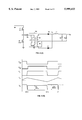
- An exemplary form of such converter is shown in FIG. 1 at 10.
- the electronic power switches S1 and S2 may be MOSFET or other well known types of electronically controllable, high speed switches and are serially connected across a source 12 of dc power (battery or rectifier coupled to ac source).
- a junction intermediate the switches S1, S2 is connected to one terminal of primary winding N p of a power transformer TR through a series capacitor Cb.
- Transformer TR has a pair of substantially identical windings NS, and NS 2 having a common terminal at 14 connected to a relatively negative dc output terminal 16. Opposite winding end terminals 18 and 20 are connected through respective diode rectifiers D1 and D2 to one end of an output filter inductor Lf. Another end of inductor Lf connects to a relatively positive output terminal 22. A resistive load R 0 and output filter capacitor C 0 connect in parallel to the dc output terminals.
- the converter 10 operates by gating switch S1 into conduction for a controlled time interval, gating switch S1 out of conduction and then gating switch S2 into conduction. Power is transferred into the converter while S1 conducts.
- the reactive components allow resonant action to occur so that current continues to the load. Due to the high switching loss and high switching noise problems associated with hard-switching operation of the devices S1, S2, the conventional HB PWM converter is not suited for high-frequency operation. In order to reduce the switching loss and noise of the converter, several zero voltage switching (ZVS) techniques have been developed.
- ZVS zero voltage switching
- Ninomiya, Matsumoto, Nakahara and Harada disclose a HB converter using magnetizing energy and asymmetrical duty cycle to achieve ZVS. Its major limitation is in requiring the use of a large output filter inductor when it operates at low duty cycles. This significantly increases the size of the converter and also results in a decrease in conversion efficiency. In addition, this converter exhibits an inherent control stability problem at light load which necessitates the use of a large pre-load for very light load or no load operation.
- Imbertson in U.S. Pat. No. 5,245,520 "Asymmetrical Duty Cycle Power Converter” discloses a HB converter which uses asymmetrical duty cycle control and a commutating inductor in series with the power transformer to achieve ZVS. Similar to the Ninomiya converter, Imbertson also requires the use of a large output filter inductor when operating at low duty cycles and exhibits an inherent control stability problem at light load. With the help of a series commutating inductor, the switch conduction loss is somewhat reduced, but ZVS can be easily lost as load current decreases.
- FIGS. 2A and 2B show the circuit schematic and switching waveforms respectively of the ZVS HB converter disclosed in the Ninomiya article.
- Two primary switches S1 and S2 are turned on and off complementary with certain dead times (t0-t1 and t2-t3) in between to allow ZVS to occur.
- the power transformer TR has one primary winding N P and two identical secondary windings NS1 and NS2.
- the transformer is designed to have a fairly low magnetizing inductance so that the peak magnetizing current at either switch S1 or S2 turn-off is greater than the reflected output filter inductor Lf current. In this way, ZVS operation can be maintained even at light load.
- V B the voltage, appearing in front of the output filter inductor L f is equal to DV in /(Np/Ns) and (1-D)V in /(Np/Ns), respectively, where D is the duty cycle of switch S1 in percent on-time and NP and NS are the number of turns in the primary and each secondary winding, respectively.
- D the duty cycle of switch S1 in percent on-time
- NP and NS are the number of turns in the primary and each secondary winding, respectively.
- the Ninomiya HB converter shown in FIG. 2A has a voltage conversion-ratio characteristic as shown in FIG. 3. It can be seen that the converter has a maximum gain at 50% duty cycle. In order to accommodate certain load or line transient response requirements as well as component tolerances, the converter is typically operated at around 35% duty cycle even if the steady-state input voltage V IN is fixed. Considering that in most applications the input voltage has a certain variation range, the steady-state duty cycle is often less than 30%. With such a low duty cycle, V B will be much high than Vo during S1 ON period and much lower than Vo during S1 OFF period. As a result, the converter requires the use of a large L f to meet adequate efficiency and filtering requirement. This significantly increases the size and cost of the converter and also results in higher power losses.
- Ninomiya converter shown in FIG. 2A Another drawback of the Ninomiya converter shown in FIG. 2A is that it has an inherent control stability problem at very light load or no load. As a result, the converter requires the use of either a pre-load resistor which is simple but very lossy or an active pre-load which is very complicated and expensive to implement.
- This invention discloses an improved HB converter that overcomes the above-mentioned drawbacks of the prior art HB converters.
- the present invention is illustrated in a variety of half-bridge, dc-to-dc converter circuits such as a zero-voltage switching, half-bridge, pulse width modulated dc-to-dc converter comprising a transformer having a primary winding and first and second secondary windings.
- the first secondary winding has a greater number of winding turns than the second secondary winding.
- First and second controllable switching devices are connected for alternately coupling one terminal of the primary winding to one of a pair of relatively positive and relatively negative dc input terminals.
- First and second rectifiers are coupled in series circuit with one terminal of a respective one of the first and second secondary windings and a first dc output terminal.
- each of the first and second secondary windings is connected to a second dc output terminal.
- capacitance coupled with reactance of the primary winding is used to establish a resonant circuit to effect zero voltage switching of the first and second switching devices.
- the invention further discloses a pre-load circuit for use with the dc-to-dc converter in order to maintain minimum current for a broad range of output loading.
- FIG. 1 illustrates an exemplary form of half-bridge, pulse-width modulated, dc-dc converter
- FIG. 2A is a simplified schematic of another form of zero voltage switching, half-bridge, pulse-width modulated, dc-dc converter;
- FIG. 2B illustrates the switching waveforms occurring in the converter of FIG. 2A
- FIG. 3 is a graph illustrating the voltage conversion characteristics of the converter of FIG. 2A;
- FIG. 4A is a simplified schematic representation of one form of half-bridge, zero voltage switching, pulse-width modulated, dc-dc converter incorporating at least some of the teachings of the present invention
- FIG. 4B illustrates various voltage and current waveforms occurring in the converter of FIG. 4A
- FIG. 5 is a graph comparing the value of ripple current in a converter output as a function of switching duty cycle for the converter of FIG. 2A and FIG. 4A;
- FIG. 6 is a simplified schematic representation of a zero voltage switching, pulse width modulated dc-dc converter incorporating an active pre-load circuit in accordance with at least some of the teachings of the present invention
- FIG. 7 is a graph comparing pre-load control voltage to converter feedback control voltage as a function of converter output current
- FIG. 8 illustrates an application of the active pre-load circuit of FIG. 6 applied to a multiple output flyback converter
- FIG. 9A illustrates another form of active pre-load circuit as applied to a converter of the type illustrated in FIGS. 2A and 4A;
- FIG. 9B illustrates voltage and current waveforms occurring in the converter circuit of FIG. 9A.
- FIG. 4A is a simplified circuit diagram of one form of an HB-ZVS-PWM converter 20 incorporating at least some of the teachings of the present invention.
- the converter 20 includes two power switches S1 and S2, a dc-blocking capacitor Cb, a power transformer TR, two rectifying diodes D1 and D2, an output filter inductor L f , and an output filter capacitor Co.
- the power transformer TR' differs from the transformer TR of FIG. 2A by having two secondary windings N S1 , N S2 with different numbers of turns.
- FIG. 4B illustrates the switching waveforms for the converter 20.
- the converter 20 also uses the energy stored in the transformer TR' magnetizing inductance to achieve ZVS.
- V B at the diode side of inductor L f is given by: ##EQU1## where D is the ON time of switch S1 in percent duty cycle, 1-D is the ON time of switch S2 in percent duty cycle, N P is the number of primary winding turns of transformer TR', N S1 is the number of turns of winding N S1 and N S2 is the number of turns of winding N S2 .
- the converter 20 shown in FIG. 4A requires a much smaller inductor L f than the prior art HB converters.
- the converter of FIG. 4A may receive an input voltage varying from 320 to 380 volts and produce an output voltage of 18 volts with a maximum output power of about 65 watts.
- the switching devices S1 and S2 may be type IRF830 MOSFET devices, the dc blocking capacitor Cb is typically 0.1 ⁇ fd at 250 volts rated voltage, the transformer primary winding may have 56 turns while the two secondary windings NS1 and NS2 may have five turns and nine turns.
- the line filter Lf is selected to be 40 ⁇ H and the output capacitor Co is 390 ⁇ fd.
- FIG. 5 compares the typical L f current ripple between the converters 10 and 20, where line A represents converter 10 and line B represents converter 20. It is assumed that in both converters the duty cycle needs to vary from 20% to 50% in order to accommodate certain input voltage and load current variations, and the nominal steady-state duty cycle is 35% (0.35).
- the converter 20 has zero ⁇ I Lf , meaning the circuit has minimized AC conduction losses (which are associated with the amplitude of ⁇ I Lf ) and core loss in the output filter inductor L f . Therefore, the converter 20 of FIG. 4A provides size, efficiency, and cost advantages over the converter 10 of FIG. 2A.
- Another aspect of this invention is associated with the light load operation of a ZVS HB converter using asymmetrical duty cycle control.
- the ZVS HB converter of the type shown in FIGS. 2A and 4A exhibit an inherent control stability problem which causes converter oscillations at very light load. This usually happens when the load current becomes so low that the L f current enters a discontinuous conduction mode (DCM) and the duty cycle D of the switching devices becomes very low.
- DCM discontinuous conduction mode
- a pre-load is required at very light load or no load in order to maintain a minimum continuous current. In order to avoid increasing the converter power losses at heavy load, this pre-load should only be activated under light load conditions.
- a conventional way of implementing such a pre-load requires secondary-side load current sensing by using either a current transformer or a current-sensing power resistor (which is less expensive but very lossy since it is used in the main power path).
- the sensed current signal is then compared with a reference signal in a comparator to control a switch to either turn on (at light load) or turn off (at heavy load) the pre-load.
- Such a way of implementing the active pre-load is expensive, complicated, and sometimes very lossy (especially for high output current applications).
- the present invention discloses a simple, reliable, and economical approach for implementing an active pre-load.
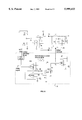
- FIG. 6 there is shown one embodiment of an active pre-load circuit 43 in accordance with the teaching of the present invention as applied to a converter 40 of the type shown in FIG. 4A.
- the inventive circuit uses only four components--a transistor Q, a pre-load resistor R P , a gate resistor R4, and a zener diode Dz--to form an active pre-load.
- the transistor Q is used as a switch to selectively couple the pre-load resistor R P across the converter output terminals.
- the zener diode D Z and gate resistor R4 are selected to gate transistor Q into conduction when the converter output voltage drops below a selected threshold.
- R1 and R2 form a resistive voltage divider to sense the converter output voltage and provide a signal representative of the converter output voltage.
- Operation of the converter 40 is established by a control circuit 45 which includes three integrated circuits IC1, IC2 and IC3, a gate driver circuit 48 and several passive components.
- the circuit IC1 is a secondary-side operational amplifier (Op-Amp) which compares the output voltage representative signal against a reference voltage V REF1 .
- Op-Amp secondary-side operational amplifier
- secondary-side refers to that portion of the converter 40 connected to the transformer TR secondary windings NS1 and NS2
- primary-side refers to that portion of the converter connected to the transformer primary winding N P .
- the output signal of Op-Amp IC1 V X is transferred to the transformer primary side through an opto-coupler IC2.
- the op-amp IC1 is a conventional operational amplifier having a feedback element Z f1 coupled between an inverting input terminal and an output terminal. As shown, the voltage representative signal is applied to the op-amp inverting input terminal and the reference voltage signal N ref1 is applied to a non-inverting input terminal.
- the reference voltage V ref1 is preferably developed by a separate electronic circuit (not shown) in a well known manner.
- the output signal V X is developed at the op-amp IC1 output terminal.
- the signal V X is coupled through series resistor R3 to an input terminal of opto-coupler IC2.
- Coupler IC2 develops an output signal at terminal 42 across the resistor R5 and this output signal is coupled to an inverting input terminal of a second op-amp 44 through a resistor R6.
- Op-amp 44 is part of an integrated pulse width modulation (PWM) signal generator IC3 which includes a comparator 46.
- PWM pulse width modulation
- the non-inverting input terminal of op-amp 44 is coupled to another voltage reference source V ref2 .
- a feedback element Z f2 couples the op-amp 44 inverting input to the op-amp output.
- the op-amp 44 output voltage V y1 is coupled to a non-inverting input terminal of comparator 46 while a sawtooth ramp signal is coupled to the inverting input terminal of comparator 46.
- the comparator 46 generates a conventional PWM signal whose characteristic is determined by the magnitude of the converter output voltage, i.e., the PWM signal is such as to gate the switches S1, S2 in a manner to regulate the converter output voltage to a desired value.
- a conventional gate driver circuit 48 converts the PWM signal into appropriate gate drive signals for application to the electronic switches S1, S2.
- Z 1 f and Z 2 f are selected in such a way that the secondary-side Op-Amp IC1 has an almost infinite DC gain but that the primary side op-amp 44 has a low DC gain.
- the high gain of op-amp IC1 assures that any small deviation of output voltage is transformed into an appropriate control signal so as to adjust the output voltage to the regulated value.
- the steady-state voltage V X of the secondary side Op-Amp IC1 is proportional to the voltage V y , as shown in FIG. 7. Consequently, control switch Q for the pre-load resistance R P can be turned on and off automatically if the zener diode D Z has an adequate threshold voltage.
- the threshold voltage of diode D Z should be selected approximately at:
- V eb is the emitter-to-base bias voltage of the transistor Q.
- V X is greater than V X crit , so the transistor Q is off and the pre-load is disabled.
- the load current is below I O crit , transistor Q is turned on and the pre-load resistor R P is connected across the converter output terminals.
- FIG. 8 shows a typical circuit diagram for a multiple-output flyback converter 50.
- the control circuit 45 senses and tightly regulates the main output voltage, Vo1, from main winding NS1.
- Vo1 main output voltage
- the duty cycle of the converter switch S also decreases.
- the output voltage Vo2 from auxiliary winding NS2 and the self-bias voltage Vc from the tertiary winding N P1 also decrease.
- the converter 50 If the main winding NS1 load current continues to decrease, the converter 50 often experiences two common problems. First, the converter 50 will experience a cross-regulation problem, i.e., the voltage Vo2 will fall below its specified minimum value as the main winding NS1 load current becomes too low. Second, the converter 50 will run into a hic-up mode during which the converter output voltage loses control and swings up and down irregularly. The second problem occurs when the control bias voltage Vc becomes too low to adequately support the control IC's, i.e., IC1, IC2 and IC3 in the control circuit 45. These two problems are in many applications. To solve these problems without increasing the converter power loss at heavy load it requires the use of an active pre-load.
- the active pre-load circuit illustrated in FIG. 6 can be directly applied here, as shown in FIG. 8. The operation of the pre-load circuit 43 in FIG. 8 is essentially identical to its operation as described with reference to FIG. 6.
- FIG. 9A shows another embodiment of an active pre-load circuit for solving the light load operation problem of the converter 40 (or converter 30) shown in FIG. 4A.
- a PNP transistor Q2 is connected in parallel circuit with diode D2 and arranged to conduct current oppositely of current through diode D2.
- a gate resistor 54 and parallel connected accelerating capacitor 56 connect a gate terminal of transistor Q2 to terminal 18 of winding NS1 where the anode terminal of diode D1 is connected.
- the current I Lf After the current I Lf reaches zero at time t a , it becomes negative and continues to ramp down at the same rate until switch S2 is turned off at time t2. Then the negative I Lf current will decay to zero quickly by charging the junction capacitances of the rectifying diodes D1 and D2. It can be seen that the use of the transistor Q2 enables the current I Lf to go negative during switch S1 OFF period. As a result, the duty cycle of the converter is extended, and the converter becomes able to operate at very light or no load without any stability problem.
- the accelerating capacitor 56 is used to expedite the turn on and turn off of transistor Q2 and thereby reduce its switching losses.
- a small snubber such as zener diode D Z2 could be used.
- the snubber can also be implemented with resistor-capacitor-diode clamp circuit at "B".
- another way to avoid the transistor Q2 turn-off voltage spike at "B” is to add another transistor (not shown) across the rectifying diode D1. After transistor Q2 is turned off at time t3, the negative IL f current will continue to flow through the transistor across the diode D1.
Abstract
Description
V.sub.DZ =V.sub.O -V.sub.X.sup.crit -V.sub.eb
Claims (17)
Priority Applications (1)
| Application Number | Priority Date | Filing Date | Title |
|---|---|---|---|
| US09/005,669 US5999433A (en) | 1998-01-12 | 1998-01-12 | Half-bridge DC to DC converter with low output current ripple |
Applications Claiming Priority (1)
| Application Number | Priority Date | Filing Date | Title |
|---|---|---|---|
| US09/005,669 US5999433A (en) | 1998-01-12 | 1998-01-12 | Half-bridge DC to DC converter with low output current ripple |
Publications (1)
| Publication Number | Publication Date |
|---|---|
| US5999433A true US5999433A (en) | 1999-12-07 |
Family
ID=21717088
Family Applications (1)
| Application Number | Title | Priority Date | Filing Date |
|---|---|---|---|
| US09/005,669 Expired - Lifetime US5999433A (en) | 1998-01-12 | 1998-01-12 | Half-bridge DC to DC converter with low output current ripple |
Country Status (1)
| Country | Link |
|---|---|
| US (1) | US5999433A (en) |
Cited By (45)
| Publication number | Priority date | Publication date | Assignee | Title |
|---|---|---|---|---|
| US6166528A (en) * | 1999-11-02 | 2000-12-26 | Fairchild Semiconductor Corporation | Lossless current sensing in buck converters working with low duty cycles and high clock frequencies |
| EP1128535A2 (en) * | 2000-02-11 | 2001-08-29 | Oxford Magnet Technology Limited | Power converter controll loop |
| US6301131B1 (en) * | 1999-05-18 | 2001-10-09 | Funai Electric Co., Ltd. | DC power supply circuit |
| US6320764B1 (en) * | 2000-03-31 | 2001-11-20 | Yimin Jiang | Regulation circuit for a power converter and method of operation thereof |
| US6381150B2 (en) * | 1999-11-19 | 2002-04-30 | Iwatt | Isolated dual converter having primary side internal feedback for output regulation |
| US6407603B2 (en) * | 1999-09-20 | 2002-06-18 | Lockheed Martin Corporation | Analog voltage isolation circuit |
| US6407935B1 (en) * | 2000-05-30 | 2002-06-18 | Koninklijke Philips Electronics N.V. | High frequency electronic ballast with reactive power compensation |
| US20030067791A1 (en) * | 2001-09-04 | 2003-04-10 | Reinhold Elferich | Regulating device for a resonant converter |
| US6567279B2 (en) * | 2001-07-05 | 2003-05-20 | Di/Dt, Inc. | Simple and efficient isolated switching regulator for fast transient loads |
| US6642696B2 (en) * | 2001-08-03 | 2003-11-04 | Texas Instruments Incorporated | DC-DC converter with a feedback controller |
| US6807073B1 (en) | 2001-05-02 | 2004-10-19 | Oltronics, Inc. | Switching type power converter circuit and method for use therein |
| US20050077910A1 (en) * | 2003-10-10 | 2005-04-14 | Encorp, Inc. | Voltage sensing device and associated method |
| EP1530282A1 (en) * | 2003-11-06 | 2005-05-11 | Bang & Olufsen A/S | Charge mode control of a serial resonance converter |
| US20070268729A1 (en) * | 2006-05-16 | 2007-11-22 | Hang-Seok Choi | Half-bridge power converter system and method of operation |
| US20070274107A1 (en) * | 2006-05-23 | 2007-11-29 | Garner David M | Switch mode power supply controllers |
| US20070297199A1 (en) * | 2004-11-29 | 2007-12-27 | Koninklijke Philips Electronics, N.V. | Multi-Resonance Converter |
| US7317305B1 (en) * | 2005-05-18 | 2008-01-08 | Volterra Semiconductor Corporation | Method and apparatus for multi-phase DC-DC converters using coupled inductors in discontinuous conduction mode |
| US7317306B2 (en) * | 1999-12-30 | 2008-01-08 | Intel Corporation | Nonlinear adaptive voltage positioning for DC-DC converters |
| US20080012547A1 (en) * | 2006-07-11 | 2008-01-17 | System General Corp. | Detection circuit for sensing the input voltage of transformer |
| US20080130326A1 (en) * | 2005-11-14 | 2008-06-05 | Kan Sheng Kuan | Zero voltage switch method for fly-back converter |
| US20090015227A1 (en) * | 2007-07-10 | 2009-01-15 | Kae Ann Wong | Load-Induced Voltage Overshoot Detection And Correction In Switching Power Supplies |
| US20090141519A1 (en) * | 2007-11-29 | 2009-06-04 | Samsung Electro-Mechanics Co., Ltd. | Dc/dc converter |
| US20090174263A1 (en) * | 2008-01-07 | 2009-07-09 | Access Business Group International Llc | Inductive power supply with duty cycle control |
| US20090273297A1 (en) * | 2008-04-30 | 2009-11-05 | Lsi Industries, Inc. | Power factor correction and driver circuits |
| US20100117545A1 (en) * | 2008-04-30 | 2010-05-13 | Lsi Industries, Inc. | Solid State Lighting, Driver Circuits, and Related Software |
| CN101710794A (en) * | 2009-12-17 | 2010-05-19 | 北京中星微电子有限公司 | Alternating current-direct current flyback converter and loop circuit compensation method under total energy conversion mode |
| US20100188870A1 (en) * | 2003-11-06 | 2010-07-29 | Bang & Olufsen A/S | Charge mode control |
| US20110080757A1 (en) * | 2007-09-12 | 2011-04-07 | George Young | power converter |
| CN102142776A (en) * | 2010-01-29 | 2011-08-03 | 株式会社村田制作所 | Switching power-supply apparatus |
| US20130147269A1 (en) * | 2010-04-09 | 2013-06-13 | Michael Zimmermann | Modular LED Lighting System Having Emergency Light Function |
| US8547076B1 (en) | 2011-03-10 | 2013-10-01 | Volterra Semiconductor Corporation | Multiphase control systems and associated methods |
| US20130301311A1 (en) * | 2012-05-08 | 2013-11-14 | Chengdu Monolithic Power Systems Co., Ltd. | Switching mode power supply and the method thereof |
| CN103916015A (en) * | 2013-01-08 | 2014-07-09 | 产晶积体电路股份有限公司 | Control device for dual-mode power supply switching |
| US8885363B2 (en) * | 2013-01-08 | 2014-11-11 | Inno-Tech Co., Ltd. | Dual-mode switching power control device |
| CN104883065A (en) * | 2015-05-29 | 2015-09-02 | 西安交通大学 | High-frequency isolation circuit, control method thereof and solid-state transformer |
| CN104953839A (en) * | 2014-03-31 | 2015-09-30 | 上海鸣志自动控制设备有限公司 | Stable power supply circuit |
| US20150311809A1 (en) * | 2013-11-11 | 2015-10-29 | Lg Innotek Co., Ltd. | Current regulation apparatus |
| US20150357922A1 (en) * | 2014-06-05 | 2015-12-10 | Lite-On Electronics (Guangzhou) Limited | Direct current voltage conversion device |
| EP3012956A1 (en) * | 2010-03-26 | 2016-04-27 | Russell Jacques | Controller for controlling a power converter |
| CN107425724A (en) * | 2017-08-14 | 2017-12-01 | 杭州可靠性仪器厂 | Flyback sourse preloading device |
| US9966837B1 (en) | 2016-07-08 | 2018-05-08 | Vpt, Inc. | Power converter with circuits for providing gate driving |
| US10073474B2 (en) * | 2016-02-11 | 2018-09-11 | STMicroelectronics (Alps) SAS | Device for controlling a current in a load having an unknown current-vs.-voltage characteristic |
| US10813385B2 (en) * | 2018-03-09 | 2020-10-27 | Rai Strategic Holdings, Inc. | Buck regulator with operational amplifier feedback for an aerosol delivery device |
| US10814806B1 (en) * | 2014-07-22 | 2020-10-27 | Richard H. Sherratt and Susan B. Sherratt Revocable Trust Fund | DC energy transfer apparatus, applications, components, and methods |
| US11258289B2 (en) * | 2017-09-22 | 2022-02-22 | Guangdong Oppo Mobile Telecommunications Corp., Ltd. | Power supply circuit and adaptor |
Citations (4)
| Publication number | Priority date | Publication date | Assignee | Title |
|---|---|---|---|---|
| US4387418A (en) * | 1977-08-01 | 1983-06-07 | Toko, Inc. | Switching regulator |
| US4860184A (en) * | 1987-09-23 | 1989-08-22 | Virginia Tech Intellectual Properties, Inc. | Half-bridge zero-voltage switched multi-resonant converters |
| US5245520A (en) * | 1991-10-10 | 1993-09-14 | Paul Imbertson | Asymmetrical duty cycle power converter |
| US5325283A (en) * | 1992-06-08 | 1994-06-28 | Center For Innovative Technology | Novel zero-voltage-switching family of isolated converters |
-
1998
- 1998-01-12 US US09/005,669 patent/US5999433A/en not_active Expired - Lifetime
Patent Citations (4)
| Publication number | Priority date | Publication date | Assignee | Title |
|---|---|---|---|---|
| US4387418A (en) * | 1977-08-01 | 1983-06-07 | Toko, Inc. | Switching regulator |
| US4860184A (en) * | 1987-09-23 | 1989-08-22 | Virginia Tech Intellectual Properties, Inc. | Half-bridge zero-voltage switched multi-resonant converters |
| US5245520A (en) * | 1991-10-10 | 1993-09-14 | Paul Imbertson | Asymmetrical duty cycle power converter |
| US5325283A (en) * | 1992-06-08 | 1994-06-28 | Center For Innovative Technology | Novel zero-voltage-switching family of isolated converters |
Non-Patent Citations (2)
| Title |
|---|
| Static And Dynamic Analysis of Zero Voltage Switched Half Bridge Converter with PWM Control Tamotsu Ninomiya, Norio Matsumoto, Masatoshi Nakahara, Koosuke Harada 4/91/0700 0230 1991 IEEE, pp. 230 237. * |
| Static And Dynamic Analysis of Zero-Voltage-Switched Half-Bridge Converter with PWM Control Tamotsu Ninomiya, Norio Matsumoto, Masatoshi Nakahara, Koosuke Harada 4/91/0700-0230 1991 IEEE, pp. 230-237. |
Cited By (88)
| Publication number | Priority date | Publication date | Assignee | Title |
|---|---|---|---|---|
| US6301131B1 (en) * | 1999-05-18 | 2001-10-09 | Funai Electric Co., Ltd. | DC power supply circuit |
| US6407603B2 (en) * | 1999-09-20 | 2002-06-18 | Lockheed Martin Corporation | Analog voltage isolation circuit |
| US6166528A (en) * | 1999-11-02 | 2000-12-26 | Fairchild Semiconductor Corporation | Lossless current sensing in buck converters working with low duty cycles and high clock frequencies |
| US6381150B2 (en) * | 1999-11-19 | 2002-04-30 | Iwatt | Isolated dual converter having primary side internal feedback for output regulation |
| US7317306B2 (en) * | 1999-12-30 | 2008-01-08 | Intel Corporation | Nonlinear adaptive voltage positioning for DC-DC converters |
| US6421257B2 (en) | 2000-02-11 | 2002-07-16 | Oxford Magnet Technology Limited | Power converter control loop |
| EP1128535A3 (en) * | 2000-02-11 | 2002-04-03 | Oxford Magnet Technology Limited | Power converter controll loop |
| EP1128535A2 (en) * | 2000-02-11 | 2001-08-29 | Oxford Magnet Technology Limited | Power converter controll loop |
| US6320764B1 (en) * | 2000-03-31 | 2001-11-20 | Yimin Jiang | Regulation circuit for a power converter and method of operation thereof |
| US6407935B1 (en) * | 2000-05-30 | 2002-06-18 | Koninklijke Philips Electronics N.V. | High frequency electronic ballast with reactive power compensation |
| US7002815B2 (en) | 2001-05-02 | 2006-02-21 | Oltronics, Inc. | Switching type power converter circuit and method for use therein |
| US6807073B1 (en) | 2001-05-02 | 2004-10-19 | Oltronics, Inc. | Switching type power converter circuit and method for use therein |
| US20050036340A1 (en) * | 2001-05-02 | 2005-02-17 | Oltronics | Switching type power converter circuit and method for use therein |
| US6567279B2 (en) * | 2001-07-05 | 2003-05-20 | Di/Dt, Inc. | Simple and efficient isolated switching regulator for fast transient loads |
| US6642696B2 (en) * | 2001-08-03 | 2003-11-04 | Texas Instruments Incorporated | DC-DC converter with a feedback controller |
| US20030067791A1 (en) * | 2001-09-04 | 2003-04-10 | Reinhold Elferich | Regulating device for a resonant converter |
| US6829151B2 (en) * | 2001-09-04 | 2004-12-07 | Koninklijke Philips Electronics N.V. | Regulating device for a resonant converter |
| US20070096718A1 (en) * | 2003-10-10 | 2007-05-03 | Primary Integration, Llc | Voltage sensing device and associated method |
| US7759959B2 (en) | 2003-10-10 | 2010-07-20 | Primary Integration, Inc. | Voltage sensing device and associated method |
| US7176698B2 (en) * | 2003-10-10 | 2007-02-13 | Primary Integration, Llc | Voltage sensing device and associated method |
| US20050077910A1 (en) * | 2003-10-10 | 2005-04-14 | Encorp, Inc. | Voltage sensing device and associated method |
| US20070171679A1 (en) * | 2003-11-06 | 2007-07-26 | Bang & Olufsen A/S | Charge mode control of a serial resonance converter |
| US7656691B2 (en) | 2003-11-06 | 2010-02-02 | Bang & Olufsen A/S | Charge mode control of a serial resonance converter |
| WO2005046037A1 (en) * | 2003-11-06 | 2005-05-19 | Bang & Olufsen A/S | Charge mode control of a serial resonance converter |
| EP1530282A1 (en) * | 2003-11-06 | 2005-05-11 | Bang & Olufsen A/S | Charge mode control of a serial resonance converter |
| US20100188870A1 (en) * | 2003-11-06 | 2010-07-29 | Bang & Olufsen A/S | Charge mode control |
| US8411476B2 (en) | 2003-11-06 | 2013-04-02 | Bang & Olufsen A/S | Charge mode control |
| US20070297199A1 (en) * | 2004-11-29 | 2007-12-27 | Koninklijke Philips Electronics, N.V. | Multi-Resonance Converter |
| US7688600B2 (en) * | 2004-11-29 | 2010-03-30 | Nxp B.V. | Multi-Resonance converter |
| US7317305B1 (en) * | 2005-05-18 | 2008-01-08 | Volterra Semiconductor Corporation | Method and apparatus for multi-phase DC-DC converters using coupled inductors in discontinuous conduction mode |
| US7859238B1 (en) | 2005-05-18 | 2010-12-28 | Volterra Semiconductor Corporation | Method and apparatus for multi-phase DC-DC converters using coupled inductors in discontinuous conduction mode |
| US7548046B1 (en) | 2005-05-18 | 2009-06-16 | Volterra Semiconductor Corporation | Method and apparatus for multi-phase DC-DC converters using coupled inductors in discontinuous conduction mode |
| US20080130326A1 (en) * | 2005-11-14 | 2008-06-05 | Kan Sheng Kuan | Zero voltage switch method for fly-back converter |
| US20070268729A1 (en) * | 2006-05-16 | 2007-11-22 | Hang-Seok Choi | Half-bridge power converter system and method of operation |
| US7889518B2 (en) * | 2006-05-16 | 2011-02-15 | Fairchild Korea Semiconductor, Ltd. | Half-bridge power converter system and method of operation |
| US20070274107A1 (en) * | 2006-05-23 | 2007-11-29 | Garner David M | Switch mode power supply controllers |
| US7447049B2 (en) * | 2006-05-23 | 2008-11-04 | Cambridge Semiconductor Limited | Single ended flyback power supply controllers with integrator to integrate the difference between feedback signal a reference signal |
| US7671578B2 (en) * | 2006-07-11 | 2010-03-02 | System General Corp. | Detection circuit for sensing the input voltage of transformer |
| US20080012547A1 (en) * | 2006-07-11 | 2008-01-17 | System General Corp. | Detection circuit for sensing the input voltage of transformer |
| US7928714B2 (en) * | 2007-07-10 | 2011-04-19 | Texas Instruments Incorporated | Load-induced voltage overshoot detection and correction in switching power supplies |
| US20090015227A1 (en) * | 2007-07-10 | 2009-01-15 | Kae Ann Wong | Load-Induced Voltage Overshoot Detection And Correction In Switching Power Supplies |
| US20110080757A1 (en) * | 2007-09-12 | 2011-04-07 | George Young | power converter |
| US8923017B2 (en) * | 2007-09-12 | 2014-12-30 | Texas Instruments (Cork) Limited | Power converter implementing frequency smearing |
| US8395915B2 (en) * | 2007-11-29 | 2013-03-12 | Samsung Electro-Mechanics Co., Ltd. | DC/DC converter |
| US20090141519A1 (en) * | 2007-11-29 | 2009-06-04 | Samsung Electro-Mechanics Co., Ltd. | Dc/dc converter |
| US20090174263A1 (en) * | 2008-01-07 | 2009-07-09 | Access Business Group International Llc | Inductive power supply with duty cycle control |
| US10170935B2 (en) | 2008-01-07 | 2019-01-01 | Philips Ip Ventures B.V. | Inductive power supply with duty cycle control |
| US9257851B2 (en) | 2008-01-07 | 2016-02-09 | Access Business Group International Llc | Inductive power supply with duty cycle control |
| US8129864B2 (en) | 2008-01-07 | 2012-03-06 | Access Business Group International Llc | Inductive power supply with duty cycle control |
| US20110012526A1 (en) * | 2008-04-30 | 2011-01-20 | Lsi Industries, Inc. | Power factor correction and driver circuits |
| US20100117545A1 (en) * | 2008-04-30 | 2010-05-13 | Lsi Industries, Inc. | Solid State Lighting, Driver Circuits, and Related Software |
| US20090273297A1 (en) * | 2008-04-30 | 2009-11-05 | Lsi Industries, Inc. | Power factor correction and driver circuits |
| US7952293B2 (en) * | 2008-04-30 | 2011-05-31 | Lsi Industries, Inc. | Power factor correction and driver circuits |
| US8432108B2 (en) | 2008-04-30 | 2013-04-30 | Lsi Industries, Inc. | Solid state lighting, driver circuits, and related software |
| CN101710794B (en) * | 2009-12-17 | 2015-09-02 | 北京中星微电子有限公司 | AC-DC flyback converter under total energy translative mode and loop circuit compensation method thereof |
| US20130148388A1 (en) * | 2009-12-17 | 2013-06-13 | Vimicro Corporation | AC-DC flyback converter and loop compensation method thereof |
| US9236803B2 (en) * | 2009-12-17 | 2016-01-12 | Wuxi Vimicro Corporation | AC-DC flyback converter and loop compensation method thereof |
| CN101710794A (en) * | 2009-12-17 | 2010-05-19 | 北京中星微电子有限公司 | Alternating current-direct current flyback converter and loop circuit compensation method under total energy conversion mode |
| US20110188269A1 (en) * | 2010-01-29 | 2011-08-04 | Murata Manufacturing Co., Ltd. | Switching power-supply apparatus |
| CN102142776B (en) * | 2010-01-29 | 2015-08-12 | 株式会社村田制作所 | Switching power unit |
| CN102142776A (en) * | 2010-01-29 | 2011-08-03 | 株式会社村田制作所 | Switching power-supply apparatus |
| US8837174B2 (en) | 2010-01-29 | 2014-09-16 | Murata Manufacturing Co., Ltd. | Switching power-supply apparatus including switching elements having a low threshold voltage |
| US10396669B2 (en) | 2010-03-26 | 2019-08-27 | Russell Jacques | Power converter measuring the average rectified primary current |
| EP3012956A1 (en) * | 2010-03-26 | 2016-04-27 | Russell Jacques | Controller for controlling a power converter |
| US20130147269A1 (en) * | 2010-04-09 | 2013-06-13 | Michael Zimmermann | Modular LED Lighting System Having Emergency Light Function |
| US10143064B2 (en) * | 2010-04-09 | 2018-11-27 | Tridonic Ag | Modular LED lighting system having emergency light function |
| US8547076B1 (en) | 2011-03-10 | 2013-10-01 | Volterra Semiconductor Corporation | Multiphase control systems and associated methods |
| US9093909B2 (en) * | 2012-05-08 | 2015-07-28 | Chengdu Monolithic Power Systems Co., Ltd. | Switching mode power supply and the method thereof |
| US20130301311A1 (en) * | 2012-05-08 | 2013-11-14 | Chengdu Monolithic Power Systems Co., Ltd. | Switching mode power supply and the method thereof |
| CN103916015A (en) * | 2013-01-08 | 2014-07-09 | 产晶积体电路股份有限公司 | Control device for dual-mode power supply switching |
| CN103916015B (en) * | 2013-01-08 | 2018-07-03 | 产晶积体电路股份有限公司 | Bimodulus power switch control device |
| US8885363B2 (en) * | 2013-01-08 | 2014-11-11 | Inno-Tech Co., Ltd. | Dual-mode switching power control device |
| US20150311809A1 (en) * | 2013-11-11 | 2015-10-29 | Lg Innotek Co., Ltd. | Current regulation apparatus |
| US9407152B2 (en) * | 2013-11-11 | 2016-08-02 | Lg Innotek Co., Ltd. | Current regulation apparatus |
| CN104953839A (en) * | 2014-03-31 | 2015-09-30 | 上海鸣志自动控制设备有限公司 | Stable power supply circuit |
| CN104953839B (en) * | 2014-03-31 | 2017-11-28 | 上海鸣志自动控制设备有限公司 | A kind of power supply circuit of stabilization |
| US9473036B2 (en) * | 2014-06-05 | 2016-10-18 | Lite-On Electronics (Guangzhou) Limited | Direct current voltage conversion device |
| CN105226950A (en) * | 2014-06-05 | 2016-01-06 | 光宝电子(广州)有限公司 | Direct-current voltage conversion device |
| US20150357922A1 (en) * | 2014-06-05 | 2015-12-10 | Lite-On Electronics (Guangzhou) Limited | Direct current voltage conversion device |
| US10814806B1 (en) * | 2014-07-22 | 2020-10-27 | Richard H. Sherratt and Susan B. Sherratt Revocable Trust Fund | DC energy transfer apparatus, applications, components, and methods |
| CN104883065A (en) * | 2015-05-29 | 2015-09-02 | 西安交通大学 | High-frequency isolation circuit, control method thereof and solid-state transformer |
| CN104883065B (en) * | 2015-05-29 | 2017-06-06 | 西安交通大学 | A kind of high-frequency isolation circuit, its control method and solid-state transformer |
| US10073474B2 (en) * | 2016-02-11 | 2018-09-11 | STMicroelectronics (Alps) SAS | Device for controlling a current in a load having an unknown current-vs.-voltage characteristic |
| US9966837B1 (en) | 2016-07-08 | 2018-05-08 | Vpt, Inc. | Power converter with circuits for providing gate driving |
| CN107425724B (en) * | 2017-08-14 | 2023-09-01 | 浙江杭可仪器有限公司 | Flyback power supply preloading device |
| CN107425724A (en) * | 2017-08-14 | 2017-12-01 | 杭州可靠性仪器厂 | Flyback sourse preloading device |
| US11258289B2 (en) * | 2017-09-22 | 2022-02-22 | Guangdong Oppo Mobile Telecommunications Corp., Ltd. | Power supply circuit and adaptor |
| US10813385B2 (en) * | 2018-03-09 | 2020-10-27 | Rai Strategic Holdings, Inc. | Buck regulator with operational amplifier feedback for an aerosol delivery device |
Similar Documents
| Publication | Publication Date | Title |
|---|---|---|
| US5999433A (en) | Half-bridge DC to DC converter with low output current ripple | |
| Huber et al. | Single-stage, single-switch, isolated power supply technique with input-current shaping and fast output-voltage regulation for universal input-voltage-range applications | |
| EP0851566B1 (en) | Half-bridge zero-voltage-switched PWM flyback DC/DC converter | |
| US7023186B2 (en) | Two stage boost converter topology | |
| US5654880A (en) | Single-stage AC-to-DC full-bridge converter with magnetic amplifiers for input current shaping independent of output voltage regulation | |
| US5539630A (en) | Soft-switching converter DC-to-DC isolated with voltage bidirectional switches on the secondary side of an isolation transformer | |
| US6069798A (en) | Asymmetrical power converter and method of operation thereof | |
| US8009448B2 (en) | Forward-flyback converter with active-clamp circuit | |
| US4720668A (en) | Zero-voltage switching quasi-resonant converters | |
| US5541828A (en) | Multiple output converter with continuous power transfer to an output and with multiple output regulation | |
| Oruganti et al. | Soft-switched DC/DC converter with PWM control | |
| US5434768A (en) | Fixed frequency converter switching at zero voltage | |
| US4841220A (en) | Dc-to-Dc converters using multi-resonant switches | |
| Yang et al. | Isolated boost circuit for power factor correction | |
| US7518895B2 (en) | High-efficiency power converter system | |
| US5991171A (en) | DC-to-DC converters | |
| US5132888A (en) | Interleaved bridge converter | |
| US5663635A (en) | Reverse energy transfer in zero-current switching power conversion | |
| US6452814B1 (en) | Zero voltage switching cells for power converters | |
| US5448465A (en) | Switching power supply without switching induced spike voltages | |
| US20020196006A1 (en) | Volt-second balanced PFCPWM power converter | |
| US4845605A (en) | High-frequency DC-DC power converter with zero-voltage switching of single primary-side power device | |
| US20120106206A1 (en) | Power supply with single stage converter for performing power factor correction and resonant conversion | |
| US5060130A (en) | High-efficiency, high-density, power supply including an input boost power supply | |
| GB2314431A (en) | Voltage regulated isolated power supply |
Legal Events
| Date | Code | Title | Description |
|---|---|---|---|
| AS | Assignment |
Owner name: VIRGINIA POWER TECHNOLOGIES, INC., VIRGINIA Free format text: ASSIGNMENT OF ASSIGNORS INTEREST;ASSIGNORS:GUICHAO, HUA;ZHUANG, XINFU;SABLE, DANIEL M.;REEL/FRAME:008962/0627 Effective date: 19980105 |
|
| FPAY | Fee payment |
Year of fee payment: 4 |
|
| REMI | Maintenance fee reminder mailed | ||
| FEPP | Fee payment procedure |
Free format text: PETITION RELATED TO MAINTENANCE FEES GRANTED (ORIGINAL EVENT CODE: PMFG); ENTITY STATUS OF PATENT OWNER: LARGE ENTITY Free format text: PETITION RELATED TO MAINTENANCE FEES FILED (ORIGINAL EVENT CODE: PMFP); ENTITY STATUS OF PATENT OWNER: LARGE ENTITY |
|
| REIN | Reinstatement after maintenance fee payment confirmed | ||
| FP | Lapsed due to failure to pay maintenance fee |
Effective date: 20071207 |
|
| AS | Assignment |
Owner name: VPT, INC., VIRGINIA Free format text: CHANGE OF NAME;ASSIGNOR:VIRGINIA POWER TECHNOLOGIES, INC.;REEL/FRAME:020930/0746 Effective date: 19990503 |
|
| PRDP | Patent reinstated due to the acceptance of a late maintenance fee |
Effective date: 20080530 |
|
| FPAY | Fee payment |
Year of fee payment: 8 |
|
| STCF | Information on status: patent grant |
Free format text: PATENTED CASE |
|
| SULP | Surcharge for late payment | ||
| FEPP | Fee payment procedure |
Free format text: PAT HOLDER NO LONGER CLAIMS SMALL ENTITY STATUS, ENTITY STATUS SET TO UNDISCOUNTED (ORIGINAL EVENT CODE: STOL); ENTITY STATUS OF PATENT OWNER: LARGE ENTITY |
|
| REFU | Refund |
Free format text: REFUND - PAYMENT OF MAINTENANCE FEE, 12TH YR, SMALL ENTITY (ORIGINAL EVENT CODE: R2553); ENTITY STATUS OF PATENT OWNER: LARGE ENTITY |
|
| FPAY | Fee payment |
Year of fee payment: 12 |