US4969079A - Corrective device for inverter output voltage error - Google Patents
Corrective device for inverter output voltage error Download PDFInfo
- Publication number
- US4969079A US4969079A US07/472,297 US47229790A US4969079A US 4969079 A US4969079 A US 4969079A US 47229790 A US47229790 A US 47229790A US 4969079 A US4969079 A US 4969079A
- Authority
- US
- United States
- Prior art keywords
- inverter
- voltage
- circuit
- polarity
- output
- Prior art date
- Legal status (The legal status is an assumption and is not a legal conclusion. Google has not performed a legal analysis and makes no representation as to the accuracy of the status listed.)
- Expired - Lifetime
Links
Images


Classifications
-
- H—ELECTRICITY
- H02—GENERATION; CONVERSION OR DISTRIBUTION OF ELECTRIC POWER
- H02M—APPARATUS FOR CONVERSION BETWEEN AC AND AC, BETWEEN AC AND DC, OR BETWEEN DC AND DC, AND FOR USE WITH MAINS OR SIMILAR POWER SUPPLY SYSTEMS; CONVERSION OF DC OR AC INPUT POWER INTO SURGE OUTPUT POWER; CONTROL OR REGULATION THEREOF
- H02M7/00—Conversion of ac power input into dc power output; Conversion of dc power input into ac power output
- H02M7/42—Conversion of dc power input into ac power output without possibility of reversal
- H02M7/44—Conversion of dc power input into ac power output without possibility of reversal by static converters
- H02M7/48—Conversion of dc power input into ac power output without possibility of reversal by static converters using discharge tubes with control electrode or semiconductor devices with control electrode
- H02M7/53—Conversion of dc power input into ac power output without possibility of reversal by static converters using discharge tubes with control electrode or semiconductor devices with control electrode using devices of a triode or transistor type requiring continuous application of a control signal
- H02M7/537—Conversion of dc power input into ac power output without possibility of reversal by static converters using discharge tubes with control electrode or semiconductor devices with control electrode using devices of a triode or transistor type requiring continuous application of a control signal using semiconductor devices only, e.g. single switched pulse inverters
- H02M7/539—Conversion of dc power input into ac power output without possibility of reversal by static converters using discharge tubes with control electrode or semiconductor devices with control electrode using devices of a triode or transistor type requiring continuous application of a control signal using semiconductor devices only, e.g. single switched pulse inverters with automatic control of output wave form or frequency
- H02M7/5395—Conversion of dc power input into ac power output without possibility of reversal by static converters using discharge tubes with control electrode or semiconductor devices with control electrode using devices of a triode or transistor type requiring continuous application of a control signal using semiconductor devices only, e.g. single switched pulse inverters with automatic control of output wave form or frequency by pulse-width modulation
Definitions
- This invention relates to a corrective device for an inverter output voltage error wherein the error of an inverter output voltage attributed to a short-circuit preventive period is detected and is corrected so as to become smaller.
- FIG. 1 is a block connection diagram in which a prior-art inverter control circuit shown in, for example, Collection of Papers of ⁇ Intelec 83 ⁇ (Oct. 18-21, Tokyo), pp. 205-212, Sekino et al.; Inverter Output Voltage Waveform Closed Loop Control Technique, is redrafted.
- numeral 1 designates an inverter main circuit.
- Numerals 2 and 3 designate a reactor and a capacitor, respectively, which constitute an A.C. filter.
- Numeral 4 indicates a D.C. power source, numeral 5 a load, numeral 7 a drive circuit for the inverter main circuit 1, numeral 8 an A.C.
- reference voltage generator circuit for generating a reference voltage having the shape of a sinusoidal wave, and numeral 9 an amplifier.
- Shown at numeral 10 is a PWM (pulse-width modulation) circuit, which is configured of a comparator circuit 10a and a carrier wave generator circuit 10b.
- FIG. 2 shows a diagram of the conventional arrangement of the inverter main circuit 1.
- This circuit has transistors 17, 18, 19 and 20, and feedback diodes 17a, 18a, 19a and 20a.
- the load 5, and the reactor 2 and capacitor 3 of the A.C. filter are incorporated as illustrated in the figure.
- Numeral 14 indicates a D.C. supply voltage V D .
- a sinusoidal output voltage 15 corresponding to the control output of the PWM circuit 10 is produced across the terminals of the capacitor 3. Meanwhile, the amplifier 9 and the PWM circuit 10 control the switching of the inverter main circuit 1 so that the output voltage may agree with the sinusoidal wave reference of the A.C. reference voltage generator circuit 8.
- the PWM circuit 10 is constructed of the comparator circuit 10a and the circuit 10b for generating a triangular carrier wave, and it determines the switching point of time of PWM on the basis of a substantially sinusoidal signal from the amplifier 9 as has been obtained by amplifying the deviation of the output voltage.
- the amplifier 9 has only a finite gain from the standpoint of stability. Therefore, the inverter operates in such a manner that the output voltage thereof follows up the reference voltage of the A.C. reference voltage generator circuit 8 with some deviation from the reference voltage.
- Waveforms in FIG. 3 represent the ideal values (in a solid line) and actual values (in a broken line) of a potential which is applied to a point a at one end of the load 5, under the assumption that the middle point of the D.C. power source V D in FIG. 2 is at the ground potential. Further, a sinusoidal wave represents a load current I.
- the transistors 17 and 20 are "on", and hence, a voltage of +V D /2 is applied to the point a of the load 5.
- a voltage of -V D /2 is applied to a point b at the other end of the load 5, so that a voltage of +V D is eventually applied across the load 5.
- the potentials of the points a and b are actually influenced by the reactor 2 and the capacitor 3.
- the transistors 19 and 18 are "on", and hence, the voltage of -V D /2 is applied to the point a of the load 5.
- the voltage of +V D /2 is applied to the point b, so that a voltage of -V D is eventually applied across the load 5.
- the solid-line rectangular wave in FIG. 3 is a waveform at the point a in the case where the above two statuses are alternately repeated under the condition of a null transition time.
- a short-circuit preventive period T d is set at the transition between the two statuses in order to avoid the overcurrent breakdown of the transistors attributed to the "on” and “off” delays of the individual transistors.
- the overcurrent breakdown is elucidated as follows: By way of example, in the course of the transition from the status under which the transistors 17 and 20 are “on” with the transistors 18 and 19 being “off”, to the status under which the transistors 17 and 20 are “off” with the transistors 18 and 19 being “on”, the turn-off of the transistor 17 or 20 is assumed to be delayed with respect to the turn-on of the transistor 18 or 19.
- the short-circuit preventive period T d is so selected that the turn-on of the transistor to change-over from the "off" state to the "on” state is retarded, thereby to prevent the occurrence of the moment at which the transistor 17 or 19 connected to the plus side of the D.C. power source 4 and the transistor 18 or 20 connected to the minus side thereof are both turned "on".
- the rectangular wave indicated by the broken line in FIG. 3 is the actual voltage which is applied to the point a in the case of setting the short-circuit preventive period T d .
- the transistors 17 and 20 change from the “on” states into the “off” states at the point of time of a transition 22, whereupon the transistors 18 and 19 turn “on” from the “off” states with the delay T d .
- T d the short-circuit preventive period
- all the transistors are "off", but the load current I continues to flow from the point a to the point b on the basis of the reactor 2 for the filter and the inductance of the load 5.
- the path of this load current I extends along the minus side of the D.C. power source 4 ⁇ the diode 18a ⁇ the load 5 ⁇ the diode 19a ⁇ the plus side of the D.C. power source 4.
- the transistors 18 and 19 change from the “on” states into the “off” states in a period of time 24, whereupon the transistors 17 and 20 turn “on” from the “off” states with the delay of the short-circuit preventive period T d . Also during this short-circuit preventive period T d , all the transistors are “off", and the direction of the current is the same as in the foregoing, so that the potential of the point a becomes -V D /2 similarly to the above. The transistors 17 and 20 turn “on” after the short-circuit preventive period T d , so that the potential of the point a becomes +V D /2.
- the potential of the point a delays for the short-circuit preventive period T d relative to the ideal value.
- an error voltage ascribable to this delay has a minus value and develops every cycle of the rectangular wave.
- the average of such minus values corresponds to the first half of the waveform of a mean error voltage (V TD ) 26.
- the prior-art corrective device for the inverter output voltage error is constructed as described above, all the transistors across both the poles of individual arms are turned “off” for the predetermined short-circuit preventive period (T d ) so as to cease the inverter output voltage for the purpose of preventing the arms from short-circuiting during the commutations of the transistors.
- T d predetermined short-circuit preventive period
- This invention has been made in order to eliminate the problem as mentioned above, and has for its object to provide a corrective device for an inverter output voltage error which can correct the error of an inverter output voltage attributed to a short-circuit preventive period T d .
- the corrective device for an inverter output voltage error consists in that a current sensor is connected in series with the output of an inverter, that the polarity of a current detected by the current sensor is discriminated by polarity decision means, while a value corresponding to an input D.C. voltage is found by a D.C. voltage sensor, that a signal with the polarity of the value inverted according to the discriminated result delivered from the polarity decision means is generated by a polarity inverter circuit, and that the signal is applied as a correction signal to the PWM (pulse-width modulation) circuit of the inverter so as to correct the output voltage error.
- PWM pulse-width modulation
- the inverter output current is detected by the current sensor, the correction voltage required for correcting the error of the inverter output voltage is generated on the basis of the voltage level of a D.C. power source and a polarity change command obtained by deciding the polarity of the detected current by means of the polarity decision circuit, and this correction voltage is applied to the PWM circuit of the inverter so as to correct the output voltage error.
- FIG. 1 is a block diagram of a prior-art inverter control circuit
- FIG. 2 is a diagram of the conventional arrangement of an inverter main circuit
- FIG. 3 is a diagram of the waveforms of essential portions for explaining the prior art and this invention.
- FIG. 4 is a block diagram of an inverter control circuit showing an embodiment of this invention.
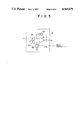
- FIG. 5 is a detailed circuit diagram of a polarity inverter circuit shown in FIG. 4.
- FIG. 4 in which the same portions as in FIG. 1 are denoted by the same symbols, numeral 6 designates a CT (current transformer) being a current sensor which is connected in series with the output circuit of an inverter, numeral 11 a comparator circuit being polarity decision means for deciding the polarity of an output current detected by the CT 6, numeral 12 a D.C. voltage sensor which detects the voltage level of the D.C. power source 4, and numeral 13 a polarity inverter circuit which inverts the polarity of the output of the D.C. voltage sensor 12 in accordance with the output state of the comparator circuit 11.
- FIG. 5 shows an embodiment of the polarity inverter circuit 13, which comprises an operational amplifier 51, fixed resistors 52-54 and an analog switch 55.
- the mean error voltage V TD at numeral 26 attributed to the short-circuit preventive period T d at numeral 25 becomes identical in phase and opposite in polarity to the inverter output current I at numeral 16 as illustrated in FIG. 3, the polarity of the current is discriminated by the comparator circuit 11.
- the mean error voltage V TD 26 corresponds to the average with respect to time, of the difference between the area of the actual inverter voltage waveform V UR at numeral 28 and that of the ideal inverter voltage waveform V UI at numeral 27, and the following relationship holds:
- V TD mean error voltage.
- the total area of hatched parts G being the differences between both the waveforms is equal to the area of the hatched part of the mean error voltage V TD 26.
- the mean error voltage V TD 26 becomes proportional to the D.C. supply voltage V D at numeral 14 in FIG. 2. Therefore, when the voltage level of the D.C. power source 4 is detected and then applied to the polarity inverter circuit 13 by the D.C. voltage sensor 12, the detected D.C. input voltage e i has its polarity inverted according to the output of the comparator circuit 11. Subsequently, as illustrated in FIG. 5, when the polarity inverter circuit 13 is supplied with a polarity change command CHG from the comparator circuit 11, the analog switch 55 turns "on".
- the analog switch 55 turns "off"
- the signal which is opposite in polarity to the mean error voltage V TD 26 is obtained at the output of the polarity inverter circuit 13.
- the embodiments have referred to an example adopting a single-phase circuit as the inverter main circuit 1, a multiphase circuit may well be used.
- a multiphase circuit may well be used.
- the same effects as those of the embodiments can be achieved even with different self-extinguishing type elements such as FETs (field-effect transistors) or BIMOS (bipolar transistors/metal-oxide-semiconductor FETs).
- a corrective device for an inverter output voltage error is so constructed that a current sensor is connected in series with the output side of an inverter, that the polarity of a current flowing through the current sensor is discriminated by a comparator circuit, and that a correction signal is applied to the PWM circuit of the inverter via a polarity inverter circuit in accordance with the discriminated polarity of the current and the voltage level of a D.C. power source detected by a D.C. voltage sensor. Therefore, the invention brings forth the effects that the inverter output voltage error is permitted to be automatically corrected, and that an inverter output voltage of high efficiency can be produced.
Landscapes
- Engineering & Computer Science (AREA)
- Power Engineering (AREA)
- Inverter Devices (AREA)
Abstract
A corrective device for an inverter output voltage error in which a current sensor is connected in series with the output of an inverter, the polarity of current detected by the current sensor is discriminated by a polarity decision current, a value corresponding to an input D.C. voltage is found by a D.C. voltage sensor, a signal with the polarity of the value inverted according to the discriminated result delivered from the polarity decision current is generted by a polarity inverter circuit, and the signal is applied as a correction signal to the PWM (pulse-width modulation) circuit of the inverter so as to correct the output voltage error.
Description
This invention relates to a corrective device for an inverter output voltage error wherein the error of an inverter output voltage attributed to a short-circuit preventive period is detected and is corrected so as to become smaller.
FIG. 1 is a block connection diagram in which a prior-art inverter control circuit shown in, for example, Collection of Papers of `Intelec 83` (Oct. 18-21, Tokyo), pp. 205-212, Sekino et al.; Inverter Output Voltage Waveform Closed Loop Control Technique, is redrafted. Referring to the figure, numeral 1 designates an inverter main circuit. Numerals 2 and 3 designate a reactor and a capacitor, respectively, which constitute an A.C. filter. Numeral 4 indicates a D.C. power source, numeral 5 a load, numeral 7 a drive circuit for the inverter main circuit 1, numeral 8 an A.C. reference voltage generator circuit for generating a reference voltage having the shape of a sinusoidal wave, and numeral 9 an amplifier. Shown at numeral 10 is a PWM (pulse-width modulation) circuit, which is configured of a comparator circuit 10a and a carrier wave generator circuit 10b.
In addition, FIG. 2 shows a diagram of the conventional arrangement of the inverter main circuit 1. This circuit has transistors 17, 18, 19 and 20, and feedback diodes 17a, 18a, 19a and 20a. The load 5, and the reactor 2 and capacitor 3 of the A.C. filter are incorporated as illustrated in the figure. Numeral 14 indicates a D.C. supply voltage VD.
Next, the operation of the prior-art circuit will be described.
First, a sinusoidal output voltage 15 corresponding to the control output of the PWM circuit 10 is produced across the terminals of the capacitor 3. Meanwhile, the amplifier 9 and the PWM circuit 10 control the switching of the inverter main circuit 1 so that the output voltage may agree with the sinusoidal wave reference of the A.C. reference voltage generator circuit 8.
Besides, the PWM circuit 10 is constructed of the comparator circuit 10a and the circuit 10b for generating a triangular carrier wave, and it determines the switching point of time of PWM on the basis of a substantially sinusoidal signal from the amplifier 9 as has been obtained by amplifying the deviation of the output voltage. In actuality, the amplifier 9 has only a finite gain from the standpoint of stability. Therefore, the inverter operates in such a manner that the output voltage thereof follows up the reference voltage of the A.C. reference voltage generator circuit 8 with some deviation from the reference voltage.
Waveforms in FIG. 3 represent the ideal values (in a solid line) and actual values (in a broken line) of a potential which is applied to a point a at one end of the load 5, under the assumption that the middle point of the D.C. power source VD in FIG. 2 is at the ground potential. Further, a sinusoidal wave represents a load current I.
Referring also to FIG. 3, during a period of time 21, the transistors 17 and 20 are "on", and hence, a voltage of +VD /2 is applied to the point a of the load 5. On this occasion, a voltage of -VD /2 is applied to a point b at the other end of the load 5, so that a voltage of +VD is eventually applied across the load 5. Here, the potentials of the points a and b are actually influenced by the reactor 2 and the capacitor 3. During a period of time 23, the transistors 19 and 18 are "on", and hence, the voltage of -VD /2 is applied to the point a of the load 5. On this occasion, the voltage of +VD /2 is applied to the point b, so that a voltage of -VD is eventually applied across the load 5.
The solid-line rectangular wave in FIG. 3 is a waveform at the point a in the case where the above two statuses are alternately repeated under the condition of a null transition time.
In actuality, a short-circuit preventive period Td is set at the transition between the two statuses in order to avoid the overcurrent breakdown of the transistors attributed to the "on" and "off" delays of the individual transistors. (The overcurrent breakdown is elucidated as follows: By way of example, in the course of the transition from the status under which the transistors 17 and 20 are "on" with the transistors 18 and 19 being "off", to the status under which the transistors 17 and 20 are "off" with the transistors 18 and 19 being "on", the turn-off of the transistor 17 or 20 is assumed to be delayed with respect to the turn-on of the transistor 18 or 19. Then, the transistors 17 and 18 or the transistors 19 and 20 are simultaneously turned "on" during the period of the delay, and both the terminals of the D.C. power source 4 are short-circuited in the meantime. Consequently, the transistors 17 and 18, or 19 and 20 lead to the breakdown due to an overcurrent flowing therethrough.) The short-circuit preventive period Td is so selected that the turn-on of the transistor to change-over from the "off" state to the "on" state is retarded, thereby to prevent the occurrence of the moment at which the transistor 17 or 19 connected to the plus side of the D.C. power source 4 and the transistor 18 or 20 connected to the minus side thereof are both turned "on".
The rectangular wave indicated by the broken line in FIG. 3 is the actual voltage which is applied to the point a in the case of setting the short-circuit preventive period Td.
The transistors 17 and 20 change from the "on" states into the "off" states at the point of time of a transition 22, whereupon the transistors 18 and 19 turn "on" from the "off" states with the delay Td. During the short-circuit preventive period Td, all the transistors are "off", but the load current I continues to flow from the point a to the point b on the basis of the reactor 2 for the filter and the inductance of the load 5. As indicated by an arrow, the path of this load current I extends along the minus side of the D.C. power source 4 → the diode 18a → the load 5 → the diode 19a → the plus side of the D.C. power source 4. As a result, the potential of the point a becomes -VD /2, and that of the point b becomes +VD /2. At the point of time of the transition 22, accordingly, the same voltage waveform as the ideal value is established without the influence of the short-circuit preventive period Td.
The transistors 18 and 19 change from the "on" states into the "off" states in a period of time 24, whereupon the transistors 17 and 20 turn "on" from the "off" states with the delay of the short-circuit preventive period Td. Also during this short-circuit preventive period Td, all the transistors are "off", and the direction of the current is the same as in the foregoing, so that the potential of the point a becomes -VD /2 similarly to the above. The transistors 17 and 20 turn "on" after the short-circuit preventive period Td, so that the potential of the point a becomes +VD /2. As a result, the potential of the point a delays for the short-circuit preventive period Td relative to the ideal value. Insofar as the load current I is flowing in the same direction as in the foregoing, an error voltage ascribable to this delay has a minus value and develops every cycle of the rectangular wave. The average of such minus values corresponds to the first half of the waveform of a mean error voltage (VTD) 26.
Incidentally, in a case where the load current I is flowing in the direction opposite to the foregoing, such an error voltage arises in the period of time in which the transistors 17 and 20 change from the "on" states into the "off" states, followed by the turn-on of the transistors 18 and 19 with the delay of the short-circuit preventive period Td. Insofar as the load current I is flowing in the opposite direction, this error voltage has a plus value and develops every cycle of the rectangular wave. The average of such plus values corresponds to the latter half of the waveform of the mean error voltage VTD) 26.
Since the prior-art corrective device for the inverter output voltage error is constructed as described above, all the transistors across both the poles of individual arms are turned "off" for the predetermined short-circuit preventive period (Td) so as to cease the inverter output voltage for the purpose of preventing the arms from short-circuiting during the commutations of the transistors. As a result, the prior-art device has had such a problem that the output voltage involves the error which corresponds to the difference between the actual inverter voltage value indicated by the broken line and the ideal inverter voltage value indicated by the solid line.
This invention has been made in order to eliminate the problem as mentioned above, and has for its object to provide a corrective device for an inverter output voltage error which can correct the error of an inverter output voltage attributed to a short-circuit preventive period Td.
The corrective device for an inverter output voltage error according to this invention consists in that a current sensor is connected in series with the output of an inverter, that the polarity of a current detected by the current sensor is discriminated by polarity decision means, while a value corresponding to an input D.C. voltage is found by a D.C. voltage sensor, that a signal with the polarity of the value inverted according to the discriminated result delivered from the polarity decision means is generated by a polarity inverter circuit, and that the signal is applied as a correction signal to the PWM (pulse-width modulation) circuit of the inverter so as to correct the output voltage error.
With the corrective device for the inverter output voltage error in this invention, the inverter output current is detected by the current sensor, the correction voltage required for correcting the error of the inverter output voltage is generated on the basis of the voltage level of a D.C. power source and a polarity change command obtained by deciding the polarity of the detected current by means of the polarity decision circuit, and this correction voltage is applied to the PWM circuit of the inverter so as to correct the output voltage error.
FIG. 1 is a block diagram of a prior-art inverter control circuit;
FIG. 2 is a diagram of the conventional arrangement of an inverter main circuit;
FIG. 3 is a diagram of the waveforms of essential portions for explaining the prior art and this invention;
FIG. 4 is a block diagram of an inverter control circuit showing an embodiment of this invention; and
FIG. 5 is a detailed circuit diagram of a polarity inverter circuit shown in FIG. 4.
Throughout the drawings, the same symbols indicate identical or equivalent portions.
Now, embodiments of this invention will be described with reference to the drawings. Referring to FIG. 4 in which the same portions as in FIG. 1 are denoted by the same symbols, numeral 6 designates a CT (current transformer) being a current sensor which is connected in series with the output circuit of an inverter, numeral 11 a comparator circuit being polarity decision means for deciding the polarity of an output current detected by the CT 6, numeral 12 a D.C. voltage sensor which detects the voltage level of the D.C. power source 4, and numeral 13 a polarity inverter circuit which inverts the polarity of the output of the D.C. voltage sensor 12 in accordance with the output state of the comparator circuit 11. In addition, FIG. 5 shows an embodiment of the polarity inverter circuit 13, which comprises an operational amplifier 51, fixed resistors 52-54 and an analog switch 55.
Next, the operation of the corrective device of this invention will be described. Since the mean error voltage VTD at numeral 26 attributed to the short-circuit preventive period Td at numeral 25 becomes identical in phase and opposite in polarity to the inverter output current I at numeral 16 as illustrated in FIG. 3, the polarity of the current is discriminated by the comparator circuit 11. The mean error voltage V TD 26 corresponds to the average with respect to time, of the difference between the area of the actual inverter voltage waveform VUR at numeral 28 and that of the ideal inverter voltage waveform VUI at numeral 27, and the following relationship holds:
V.sub.UR =V.sub.UI +V.sub.TD
where
VUR ; actual inverter voltage waveform 28,
VUI ; ideal inverter voltage waveform 27,
VTD ; mean error voltage.
In other words, the total area of hatched parts G being the differences between both the waveforms is equal to the area of the hatched part of the mean error voltage V TD 26. In addition, the mean error voltage V TD 26 becomes proportional to the D.C. supply voltage VD at numeral 14 in FIG. 2. Therefore, when the voltage level of the D.C. power source 4 is detected and then applied to the polarity inverter circuit 13 by the D.C. voltage sensor 12, the detected D.C. input voltage ei has its polarity inverted according to the output of the comparator circuit 11. Subsequently, as illustrated in FIG. 5, when the polarity inverter circuit 13 is supplied with a polarity change command CHG from the comparator circuit 11, the analog switch 55 turns "on". Thus, the polarity inverter circuit 13 functions as an inverter and produces a D.C. output voltage eo =-ei. In a case where the polarity change command is not supplied, the analog switch 55 turns "off", and the polarity inverter circuit 13 functions as a noninverting circuit and produces an output voltage eo =-ei. That is, the polarity inverter circuit 13 delivers the plus polarity when the current polarity being the output signal of the comparator circuit 11 is plus, and it delivers the minus polarity when the current polarity is minus. As a result, the signal which is opposite in polarity to the mean error voltage V TD 26 is obtained at the output of the polarity inverter circuit 13.
Although the embodiments have referred to an example adopting a single-phase circuit as the inverter main circuit 1, a multiphase circuit may well be used. Besides, although an example employing the transistors 17, 18, 19 and 20 as the switching elements has been explained, the same effects as those of the embodiments can be achieved even with different self-extinguishing type elements such as FETs (field-effect transistors) or BIMOS (bipolar transistors/metal-oxide-semiconductor FETs).
As described above, according to this invention, a corrective device for an inverter output voltage error is so constructed that a current sensor is connected in series with the output side of an inverter, that the polarity of a current flowing through the current sensor is discriminated by a comparator circuit, and that a correction signal is applied to the PWM circuit of the inverter via a polarity inverter circuit in accordance with the discriminated polarity of the current and the voltage level of a D.C. power source detected by a D.C. voltage sensor. Therefore, the invention brings forth the effects that the inverter output voltage error is permitted to be automatically corrected, and that an inverter output voltage of high efficiency can be produced.
Claims (1)
1. In a corrective device for an inverter output voltage error wherein the error of an output voltage of an inverter for changing a D.C. voltage into an A.C. voltage, the error being ascribable to a short-circuit preventive period, is controlled; a corrective device for an inverter output voltage error comprising a current sensor which detects an output current of said inverter, polarity decision means for discriminating a polarity of the inverter output current detected by said current sensor, a D.C. voltage sensor which detects a D.C. voltage of said inverter, and a polarity inverter circuit which receives an output of said polarity decision means and an output of said D.C. voltage sensor and by which a signal with a polarity of the output of said D.C. voltage sensor inverted in accordance with the output state of said polarity decision means is supplied as a correction signal to a PWM (pulse-width modulation) circuit of said inverter.
Applications Claiming Priority (2)
| Application Number | Priority Date | Filing Date | Title |
|---|---|---|---|
| JP1140805A JPH0728537B2 (en) | 1989-06-02 | 1989-06-02 | Inverter output voltage error correction device |
| JP1-140805 | 1989-06-02 |
Publications (1)
| Publication Number | Publication Date |
|---|---|
| US4969079A true US4969079A (en) | 1990-11-06 |
Family
ID=15277153
Family Applications (1)
| Application Number | Title | Priority Date | Filing Date |
|---|---|---|---|
| US07/472,297 Expired - Lifetime US4969079A (en) | 1989-06-02 | 1990-01-30 | Corrective device for inverter output voltage error |
Country Status (4)
| Country | Link |
|---|---|
| US (1) | US4969079A (en) |
| JP (1) | JPH0728537B2 (en) |
| KR (1) | KR930009072B1 (en) |
| CA (1) | CA2016479C (en) |
Cited By (11)
| Publication number | Priority date | Publication date | Assignee | Title |
|---|---|---|---|---|
| US5105352A (en) * | 1989-11-07 | 1992-04-14 | Otis Elevator Company | Offset correction circuit of pwm inverter |
| US5191519A (en) * | 1991-03-27 | 1993-03-02 | Kabushiki Kaisha Toshiba | Current sharing control in a parallel inverter system |
| EP0533403A2 (en) * | 1991-09-17 | 1993-03-24 | Otis Elevator Company | Blanking interval voltage deviation compensator for inverters and converters |
| US5229929A (en) * | 1990-11-30 | 1993-07-20 | Honda Giken Kogyo Kabushiki Kaisha | Output peak current correction for PWM invertors |
| US5355299A (en) * | 1992-07-22 | 1994-10-11 | Ansaldo-Un'azienda Finmeccanica S.P.A. | Circuit device for preventing saturation of the transformer in a dc/ac converter having a feedback-regulated inverter |
| US5388041A (en) * | 1992-05-26 | 1995-02-07 | Ansaldo-Un'azienda Finmeccanica S.P.A. | Method and a circuit for controlling an inverter to switch in the sliding mode and by PWM with a three-level output voltage |
| US5436819A (en) * | 1991-07-25 | 1995-07-25 | Mitsubishi Denki Kabushiki Kaisha | Apparatus for and method of compensating for an output voltage error in an inverter output |
| US5490055A (en) * | 1993-03-03 | 1996-02-06 | At&T Corp. | Multiloop feedback control apparatus for DC/DC converters with frequency-shaping band pass current control |
| EP1696547A1 (en) * | 2003-12-17 | 2006-08-30 | Toshiba Lighting & Technology Corporation | Discharge lamp operation device and lighting fixture |
| CN106787725A (en) * | 2016-12-30 | 2017-05-31 | 成都芯源系统有限公司 | Multiphase parallel power supply system, single-chip switch integrated circuit and current sharing method |
| CN113890400A (en) * | 2021-10-18 | 2022-01-04 | 阳光电源股份有限公司 | Inverter, control method thereof and power generation system |
Families Citing this family (2)
| Publication number | Priority date | Publication date | Assignee | Title |
|---|---|---|---|---|
| JP2756049B2 (en) * | 1991-07-25 | 1998-05-25 | 三菱電機株式会社 | Inverter output voltage error correction device |
| JPH09149923A (en) * | 1995-11-29 | 1997-06-10 | Tsurukameya:Kk | Cinerary urn |
Citations (10)
| Publication number | Priority date | Publication date | Assignee | Title |
|---|---|---|---|---|
| US4133025A (en) * | 1977-09-28 | 1979-01-02 | Motorola, Inc. | Pulse width modulator symmetry correction circuit and method thereof |
| US4546422A (en) * | 1982-12-28 | 1985-10-08 | Tokyo Shibaura Denki Kabushiki Kaisha | Control system for a voltage-type inverter |
| US4562386A (en) * | 1984-01-26 | 1985-12-31 | Performance Controls Company | Current sense demodulator |
| US4600984A (en) * | 1984-03-02 | 1986-07-15 | Itzchak Cohen | Two quadrant power modulator |
| US4660137A (en) * | 1984-11-13 | 1987-04-21 | Shinaro Electric Co., Ltd. | Inverter system |
| US4692855A (en) * | 1985-09-09 | 1987-09-08 | Kabushiki Kaisha Toshiba | Constant voltage and frequency type PWM inverter with minimum output distortion |
| US4729082A (en) * | 1985-11-21 | 1988-03-01 | Kabushiki Kaisha Toshiba | Control device for power converter |
| US4729084A (en) * | 1986-05-19 | 1988-03-01 | Mitsubishi Denki Kabushiki Kaisha | Inverter apparatus |
| US4791546A (en) * | 1987-12-23 | 1988-12-13 | Dci Technology | Voltage regulator circuit |
| US4803611A (en) * | 1987-02-12 | 1989-02-07 | Mitsubishi Denki Kabushiki Kaisha | Apparatus for correcting DC component of output voltage in inverter |
-
1989
- 1989-06-02 JP JP1140805A patent/JPH0728537B2/en not_active Expired - Fee Related
-
1990
- 1990-01-30 US US07/472,297 patent/US4969079A/en not_active Expired - Lifetime
- 1990-05-10 CA CA002016479A patent/CA2016479C/en not_active Expired - Fee Related
- 1990-06-02 KR KR1019900008148A patent/KR930009072B1/en not_active IP Right Cessation
Patent Citations (10)
| Publication number | Priority date | Publication date | Assignee | Title |
|---|---|---|---|---|
| US4133025A (en) * | 1977-09-28 | 1979-01-02 | Motorola, Inc. | Pulse width modulator symmetry correction circuit and method thereof |
| US4546422A (en) * | 1982-12-28 | 1985-10-08 | Tokyo Shibaura Denki Kabushiki Kaisha | Control system for a voltage-type inverter |
| US4562386A (en) * | 1984-01-26 | 1985-12-31 | Performance Controls Company | Current sense demodulator |
| US4600984A (en) * | 1984-03-02 | 1986-07-15 | Itzchak Cohen | Two quadrant power modulator |
| US4660137A (en) * | 1984-11-13 | 1987-04-21 | Shinaro Electric Co., Ltd. | Inverter system |
| US4692855A (en) * | 1985-09-09 | 1987-09-08 | Kabushiki Kaisha Toshiba | Constant voltage and frequency type PWM inverter with minimum output distortion |
| US4729082A (en) * | 1985-11-21 | 1988-03-01 | Kabushiki Kaisha Toshiba | Control device for power converter |
| US4729084A (en) * | 1986-05-19 | 1988-03-01 | Mitsubishi Denki Kabushiki Kaisha | Inverter apparatus |
| US4803611A (en) * | 1987-02-12 | 1989-02-07 | Mitsubishi Denki Kabushiki Kaisha | Apparatus for correcting DC component of output voltage in inverter |
| US4791546A (en) * | 1987-12-23 | 1988-12-13 | Dci Technology | Voltage regulator circuit |
Non-Patent Citations (2)
| Title |
|---|
| Sekino et al, "Inverter Output Voltage Waveform Closed-Loop Control Technique", INTELEC 83, Oct., 1983. |
| Sekino et al, Inverter Output Voltage Waveform Closed Loop Control Technique , INTELEC 83, Oct., 1983. * |
Cited By (18)
| Publication number | Priority date | Publication date | Assignee | Title |
|---|---|---|---|---|
| US5105352A (en) * | 1989-11-07 | 1992-04-14 | Otis Elevator Company | Offset correction circuit of pwm inverter |
| US5229929A (en) * | 1990-11-30 | 1993-07-20 | Honda Giken Kogyo Kabushiki Kaisha | Output peak current correction for PWM invertors |
| US5191519A (en) * | 1991-03-27 | 1993-03-02 | Kabushiki Kaisha Toshiba | Current sharing control in a parallel inverter system |
| US5436819A (en) * | 1991-07-25 | 1995-07-25 | Mitsubishi Denki Kabushiki Kaisha | Apparatus for and method of compensating for an output voltage error in an inverter output |
| EP0533403A2 (en) * | 1991-09-17 | 1993-03-24 | Otis Elevator Company | Blanking interval voltage deviation compensator for inverters and converters |
| US5206802A (en) * | 1991-09-17 | 1993-04-27 | Otis Elevator Company | Blanking interval voltage deviation compensator for inverters and converters |
| EP0533403A3 (en) * | 1991-09-17 | 1993-08-25 | Otis Elevator Company | Blanking interval voltage deviation compensator for inverters and converters |
| AU650162B2 (en) * | 1991-09-17 | 1994-06-09 | Otis Elevator Company | Blanking interval voltage deviation compensator for inverters and converters |
| US5388041A (en) * | 1992-05-26 | 1995-02-07 | Ansaldo-Un'azienda Finmeccanica S.P.A. | Method and a circuit for controlling an inverter to switch in the sliding mode and by PWM with a three-level output voltage |
| US5355299A (en) * | 1992-07-22 | 1994-10-11 | Ansaldo-Un'azienda Finmeccanica S.P.A. | Circuit device for preventing saturation of the transformer in a dc/ac converter having a feedback-regulated inverter |
| US5490055A (en) * | 1993-03-03 | 1996-02-06 | At&T Corp. | Multiloop feedback control apparatus for DC/DC converters with frequency-shaping band pass current control |
| EP1696547A1 (en) * | 2003-12-17 | 2006-08-30 | Toshiba Lighting & Technology Corporation | Discharge lamp operation device and lighting fixture |
| EP1696547A4 (en) * | 2003-12-17 | 2010-01-20 | Toshiba Lighting & Technology | Discharge lamp operation device and lighting fixture |
| CN106787725A (en) * | 2016-12-30 | 2017-05-31 | 成都芯源系统有限公司 | Multiphase parallel power supply system, single-chip switch integrated circuit and current sharing method |
| US10256727B2 (en) * | 2016-12-30 | 2019-04-09 | Chengdu Monolithic Power Systems Co., Ltd. | Multi-phase power supply with DC-DC converter integrated circuits having current sharing function |
| CN106787725B (en) * | 2016-12-30 | 2019-06-18 | 成都芯源系统有限公司 | Multiphase parallel power supply system, single-chip switch integrated circuit and current sharing method |
| CN113890400A (en) * | 2021-10-18 | 2022-01-04 | 阳光电源股份有限公司 | Inverter, control method thereof and power generation system |
| CN113890400B (en) * | 2021-10-18 | 2024-05-14 | 阳光电源股份有限公司 | Inverter, control method thereof and power generation system |
Also Published As
| Publication number | Publication date |
|---|---|
| JPH0728537B2 (en) | 1995-03-29 |
| CA2016479A1 (en) | 1990-12-02 |
| KR930009072B1 (en) | 1993-09-22 |
| KR910002093A (en) | 1991-01-31 |
| CA2016479C (en) | 1995-08-01 |
| JPH037071A (en) | 1991-01-14 |
Similar Documents
| Publication | Publication Date | Title |
|---|---|---|
| EP0099918B1 (en) | Stepper motor control circuit | |
| US4969079A (en) | Corrective device for inverter output voltage error | |
| US5428522A (en) | Four quadrant unipolar pulse width modulated inverter | |
| EP0376726B1 (en) | Generator voltage regulator power circuit | |
| US6337804B1 (en) | Multilevel PWM voltage source inverter control at low output frequencies | |
| US10826380B2 (en) | Switching converter, circuit and method for controlling the same | |
| KR100233956B1 (en) | Voltage type inverter and that control method | |
| US5852557A (en) | Switching converter utilizing dual switch outputs | |
| US6853170B2 (en) | DC-DC converter and DC-DC converter drive circuit | |
| US6181087B1 (en) | Discharge lamp operating device | |
| JP2001037246A (en) | System incorporated inverter | |
| JP6908010B2 (en) | Switch drive | |
| JPH11235025A (en) | Switching regulator control circuit of pwm system and switching regulator | |
| JP6516182B2 (en) | Power converter circuit and power converter using the same | |
| JP3480718B2 (en) | Phase control circuit and switching regulator | |
| JPH09238481A (en) | Power converting equipment | |
| US6967852B2 (en) | Power converter with dynamic current limiting | |
| JP2760582B2 (en) | Constant voltage and constant frequency power supply | |
| JPH08103085A (en) | System interconnection type inverter controller | |
| SU1275707A1 (en) | Method of controlling stabilized inverter with choke in a.c.circuit | |
| JPH0974740A (en) | Dc power controlling device | |
| KR19980017940U (en) | Line Voltage and Current Control Device of Three-Phase Parallel Resonant Inverter | |
| SU1668975A1 (en) | Secondary electric power supply system | |
| JPH03183357A (en) | Chopper controller | |
| JP2004289946A (en) | Motor drive circuit |
Legal Events
| Date | Code | Title | Description |
|---|---|---|---|
| AS | Assignment |
Owner name: MITSUBISHI DENKI KABUSHIKI KAISHA, JAPAN Free format text: ASSIGNMENT OF ASSIGNORS INTEREST.;ASSIGNORS:KIRIYAMA, MITSUO;KAWAI, JOJI;REEL/FRAME:005239/0138 Effective date: 19900120 |
|
| STCF | Information on status: patent grant |
Free format text: PATENTED CASE |
|
| FEPP | Fee payment procedure |
Free format text: PAYOR NUMBER ASSIGNED (ORIGINAL EVENT CODE: ASPN); ENTITY STATUS OF PATENT OWNER: LARGE ENTITY |
|
| FPAY | Fee payment |
Year of fee payment: 4 |
|
| FPAY | Fee payment |
Year of fee payment: 8 |
|
| FPAY | Fee payment |
Year of fee payment: 12 |