US11429021B2 - DNA nanostructure patterned templates - Google Patents
DNA nanostructure patterned templates Download PDFInfo
- Publication number
- US11429021B2 US11429021B2 US15/993,579 US201815993579A US11429021B2 US 11429021 B2 US11429021 B2 US 11429021B2 US 201815993579 A US201815993579 A US 201815993579A US 11429021 B2 US11429021 B2 US 11429021B2
- Authority
- US
- United States
- Prior art keywords
- dna
- polymer
- layer
- template
- nanostructure
- Prior art date
- Legal status (The legal status is an assumption and is not a legal conclusion. Google has not performed a legal analysis and makes no representation as to the accuracy of the status listed.)
- Active, expires
Links
Images


Classifications
-
- G—PHYSICS
- G03—PHOTOGRAPHY; CINEMATOGRAPHY; ANALOGOUS TECHNIQUES USING WAVES OTHER THAN OPTICAL WAVES; ELECTROGRAPHY; HOLOGRAPHY
- G03F—PHOTOMECHANICAL PRODUCTION OF TEXTURED OR PATTERNED SURFACES, e.g. FOR PRINTING, FOR PROCESSING OF SEMICONDUCTOR DEVICES; MATERIALS THEREFOR; ORIGINALS THEREFOR; APPARATUS SPECIALLY ADAPTED THEREFOR
- G03F7/00—Photomechanical, e.g. photolithographic, production of textured or patterned surfaces, e.g. printing surfaces; Materials therefor, e.g. comprising photoresists; Apparatus specially adapted therefor
- G03F7/0002—Lithographic processes using patterning methods other than those involving the exposure to radiation, e.g. by stamping
-
- B—PERFORMING OPERATIONS; TRANSPORTING
- B29—WORKING OF PLASTICS; WORKING OF SUBSTANCES IN A PLASTIC STATE IN GENERAL
- B29C—SHAPING OR JOINING OF PLASTICS; SHAPING OF MATERIAL IN A PLASTIC STATE, NOT OTHERWISE PROVIDED FOR; AFTER-TREATMENT OF THE SHAPED PRODUCTS, e.g. REPAIRING
- B29C33/00—Moulds or cores; Details thereof or accessories therefor
- B29C33/38—Moulds or cores; Details thereof or accessories therefor characterised by the material or the manufacturing process
- B29C33/3842—Manufacturing moulds, e.g. shaping the mould surface by machining
-
- B—PERFORMING OPERATIONS; TRANSPORTING
- B05—SPRAYING OR ATOMISING IN GENERAL; APPLYING FLUENT MATERIALS TO SURFACES, IN GENERAL
- B05D—PROCESSES FOR APPLYING FLUENT MATERIALS TO SURFACES, IN GENERAL
- B05D1/00—Processes for applying liquids or other fluent materials
- B05D1/60—Deposition of organic layers from vapour phase
-
- B—PERFORMING OPERATIONS; TRANSPORTING
- B05—SPRAYING OR ATOMISING IN GENERAL; APPLYING FLUENT MATERIALS TO SURFACES, IN GENERAL
- B05D—PROCESSES FOR APPLYING FLUENT MATERIALS TO SURFACES, IN GENERAL
- B05D5/00—Processes for applying liquids or other fluent materials to surfaces to obtain special surface effects, finishes or structures
-
- B—PERFORMING OPERATIONS; TRANSPORTING
- B32—LAYERED PRODUCTS
- B32B—LAYERED PRODUCTS, i.e. PRODUCTS BUILT-UP OF STRATA OF FLAT OR NON-FLAT, e.g. CELLULAR OR HONEYCOMB, FORM
- B32B11/00—Layered products comprising a layer of bituminous or tarry substances
- B32B11/02—Layered products comprising a layer of bituminous or tarry substances with fibres or particles being present as additives in the layer
-
- B—PERFORMING OPERATIONS; TRANSPORTING
- B32—LAYERED PRODUCTS
- B32B—LAYERED PRODUCTS, i.e. PRODUCTS BUILT-UP OF STRATA OF FLAT OR NON-FLAT, e.g. CELLULAR OR HONEYCOMB, FORM
- B32B13/00—Layered products comprising a a layer of water-setting substance, e.g. concrete, plaster, asbestos cement, or like builders' material
-
- B—PERFORMING OPERATIONS; TRANSPORTING
- B32—LAYERED PRODUCTS
- B32B—LAYERED PRODUCTS, i.e. PRODUCTS BUILT-UP OF STRATA OF FLAT OR NON-FLAT, e.g. CELLULAR OR HONEYCOMB, FORM
- B32B3/00—Layered products comprising a layer with external or internal discontinuities or unevennesses, or a layer of non-planar form; Layered products having particular features of form
Definitions
- Soft lithography uses a stamp to transfer micro- and nano-scale patterns.
- the stamp is usually fabricated by casting a liquid precursor onto a master template with patterned structures.
- Soft lithography has been well developed and widely used for nanofabrication because of its simplicity, low cost, and compatibility with a wide range of substrates, especially soft materials and nonplanar surfaces.
- the application of soft lithography is fundamentally limited by the spatial resolution and diversity of the structures on the stamp.
- SWNTs single-walled carbon nanotubes
- high-modulus ⁇ 10 MPa
- polydimethylsiloxane or PDMS as well to an acryloxy perfluoropolyether.
- SWNTs were attached to the silicon wafer through relatively weak van der Waals interaction.
- An anti-adhesion silane layer was deposited on the template substrate (a silicon wafer) when PDMS was used to reduce adhesion of PDMS to the silicon wafer.
- programmable DNA self-assembly has produced a wide range of one-dimensional (1D), two-dimensional (2D) and three-dimensional (3D) nanostructures with diverse and complex features.
- Assembled DNA nanostructures can be rationally designed and reliably synthesized. The assembly process is fast and easily implemented.
- Self-assembled DNA nanostructures may be desirable for use as a nanofabrication template because of the ease of controlling their shapes with nanometer-scale spatial resolution. Indeed, a number of approaches have been developed to transfer the pattern of DNA nanostructures to a range of materials.
- DNA nanostructures have been employed as masks to transfer the pattern to evaporated noble metal films.
- Metallization has also been achieved through wet chemistry, and the resulting metal nanostructures have been used to pattern graphene.
- DNA nanostructures have been used to modulate the rate of HF vapor phase etching to achieve pattern transfer to the SiO 2 substrate.
- adsorption of water could control the rate of chemical vapor deposition of SiO 2 and TiO 2 on the DNA nanostructures and substrate to convert the pattern of DNA nanostructures into that of inorganic oxides.
- DNA 3D nanostructures have served as molds to synthesize inorganic nanostructures with prescribed 3D shapes.
- Al 2 O 3 protected DNA nanostructures have been converted to carbon nanostructures by thermal annealing.
- a dense layer of protective layer of Al 2 O 3 was provided to prevent escape of decomposition gases during a high-temperature carbonization and thereby maintain the original conformation/shape of the underlying DNA nanostructure in the final carbonized composition.
- No forces were applied to the Al 2 O 3 or other inorganic oxide protective layer in the process of carbonization. Mechanical strength of the protective layer was not relevant to the process.
- the Al 2 O 3 or other inorganic oxide protective layer was removed after carbonization (for example, via selective etching) to provide the carbonized composition product.
- DNA nanostructures are promising templates for materials as a result of their structural complexity and diversity in the nanoscale, nanofabrication based on DNA nanostructures faces several daunting challenges.
- a potential strategy to partially overcome these problems is to establish a method to transfer complex DNA patterns to a polymer substrate.
- the resulting polymer stamps can be used as templates for the following patterning process, which reduces the cost, simplifies the fabrication process and potentially overcomes the difficulties of scalable patterning.
- a linear DNA bundle with an average height of ca. 90 nm and an average width of ca. 879 nm was employed as a master template for the fabrication of a negative replica on an unsaturated polyester resin, which was further used to pattern a polyacrylamide gel.
- the lateral dimension of the DNA bundle was relatively large (approximately 1 ⁇ m).
- the DNA patterned stamp was used only a single time.
- a method of forming a patterned device includes depositing at least one nanostructure comprising self-assembled nucleic acids formed into a predetermined conformation upon a surface of a substrate, depositing a stabilizing layer of material mechanically stronger than the at least one nanostructure over the at least one nanostructure and the surface of the substrate to form a positive pattern template, depositing a layer of a first polymer over the positive pattern template, and removing the layer of the first polymer from connection with the positive pattern template, wherein the layer of the first polymer includes a surface having a negative imprint of the positive pattern template.
- the method may further include, after removal of the layer of the first polymer, depositing a layer of a second polymer over the surface of the layer of the first polymer having the negative imprint to create a positive copy of the negative imprint upon a surface of the layer of the second polymer.
- the method may, for example, further include depositing a layer of a third polymer over the layer of the first polymer before removing the layer of the first polymer from connection with the positive pattern.
- the nucleic acids comprise or consist of deoxyribonucleic acid or DNA.
- the stabilizing layer is deposited via a thin film technique.
- the stabilizing layer may, for example, be deposited via atomic layer deposition, vacuum deposition, sputtering, chemical vapor deposition or laser assisted deposition.
- the stabilizing layer may, for example, include a metal or an oxide (for example, a metal oxide or a nonmetallic, inorganic oxide—for example, a ceramic material).
- the stabilizing layer comprises metal oxide or an inorganic oxide.
- the stabilizing layer may include aluminum oxide (Al 2 O 3 ) or silicon oxide.
- the stabilizing layer includes aluminum oxide.
- the stabilizing layer of aluminum oxide may, for example, have a thickness in the range of 2 nm to 15 nm or in the range of 3 nm to 10 nm. Even though the thin stabilizing layers hereof are formed upon a relatively mechanically weak foundation of patterned nucleic acid, the stabilizing layers were found to provide sufficient mechanical stability to allow repeated used of pattern templates hereof.
- the layer of the first polymer is deposited upon the positive pattern in solution.
- the layer of the first polymer may, for example, be deposited upon the positive pattern template via spin casting.
- the at least one nanostructure has at least one dimension of no greater than 80 nm.
- the at least one nanostructure may, for example, have at least one dimension in the range of 1 nm to 80 nm.
- a method of forming a patterned device includes depositing at least one nanostructure comprising self-assembled nucleic acids formed into a predetermined conformation upon a surface of a substrate to form a positive pattern template, the at least one nanostructure having at least one dimension of no greater than 80 nm, depositing a layer of a first polymer over the positive pattern template, and removing the layer of the first polymer from connection with the positive pattern template, wherein the layer of the first polymer includes a surface having a negative imprint of the positive pattern template.
- the at least one nanostructure may, for example, at least one dimension in the range of 1 nm to 80 nm.
- the method further includes depositing a stabilizing layer of material mechanically stronger than the at least one nanostructure over the at least one nanostructure and the surface of the substrate in forming the positive pattern template.
- the method further includes, after removal of the layer of the first polymer, depositing a layer of a second polymer over the surface of the layer of the first polymer having the negative imprint to create a positive copy of the negative imprint upon a surface of the layer of the second polymer.
- the method may, for example, further include depositing a layer of a third polymer over the layer of the first polymer before removing the layer of the first polymer from connection with the positive pattern.
- the nucleic acids comprise or consist of deoxyribonucleic acid or DNA.
- the stabilizing layer may, for example, be deposited via a thin film technique.
- the stabilizing layer may, for example, be deposited via atomic layer deposition, vacuum deposition, sputtering, chemical vapor deposition or laser assisted deposition.
- the stabilizing layer may, for example, include a metal or an inorganic oxide.
- the stabilizing layer comprises a metal or a metal oxide.
- the stabilizing layer may, for example, include aluminum oxide (Al 2 O 3 ) or silicon oxide.
- the stabilizing layer includes aluminum oxide.
- the stabilizing layer of aluminum oxide may, for example, have a thickness in the range of 2 nm to 15 nm or in the range of 3 nm to 10 nm.
- the layer of the first polymer is deposited upon the positive pattern in solution.
- the layer of the first polymer may, for example, be deposited upon the positive pattern template via spin casting.
- a patterned device includes at least one nanostructure comprising self-assembled nucleic acids formed into a predetermined conformation upon a surface of a substrate, and a stabilizing layer of material mechanically stronger than the at least one nanostructure over the at least one template structure and the surface of the substrate to form a positive pattern template.
- the patterned device may be further formed as described above.
- the patterned device may, for example, further include a layer of a first polymer deposited over the positive pattern template, wherein the layer of the first polymer is removable from connection with the positive pattern template, and wherein a removed layer of the first polymer includes a surface having a negative imprint of the positive pattern template.
- a patterned device includes at least one nanostructure including self-assembled nucleic acids formed into a predetermined conformation immobilized upon a surface of a substrate to form a positive pattern template, the at least one nanostructure having at least one dimension of no greater than 80 nm.
- the patterned device may, for example, further include a layer of a first polymer deposited over the positive pattern template, wherein the layer of the first polymer is removable from connection with the positive pattern template, and wherein a removed layer of the first polymer includes a surface having a negative imprint of the positive pattern template.
- FIG. 1 Illustrates schematically representative embodiments of a methodology and device hereof.
- FIG. 2 Illustrates an embodiment of a fabrication technique for polymer stamps using DNA nanostructures as master templates wherein the process includes: (a) Supplying a substrate such as a silicon wafer. (b) DNA is deposited on the silicon wafer. (c) A polymer film (e.g., PMMA) is spin-coated on the silicon wafer. (d) Polymer film (ca. 1 mm wide) is removed from the four edges. (e) A polydimethylsiloxane (PDMS) film adheres to the polymer film as a flexible backing. (f) Drops of water are added to one edge of the exposed silicon wafer and the PDMS/polymer film is peeled off.
- a substrate such as a silicon wafer.
- DNA is deposited on the silicon wafer.
- a polymer film e.g., PMMA
- Polymer film e.g., PMMA
- Polymer film e. 1 mm wide
- PDMS polydimethylsiloxane
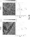
- FIG. 3A illustrates atomic force microscopy or AFM height (left) and phase (right) images of DNA nanotubes deposited on the silicon wafer in fabrication of PMMA stamps (top) by replication over DNA nanotubes wherein the scale bars represent 300 nm, corresponding cross-sections are shown at the bottom, and white lines in the top images indicated the position where the cross-section analyses were determined.
- FIG. 3B illustrates AFM height (left) and phase (right) images of the replica of nanotube patterns on PMMA stamps (top) wherein the scale bars represent 300 nm and corresponding cross-sections are shown at the bottom.
- FIG. 4A illustrates a model of 2D DNA brick crystal in the fabrication of PMMA stamps by replication over 2D DNA brick crystals wherein the repeating unit is labeled as the shaded region.
- FIG. 4B illustrates a side view of the model of the 2D DNA brick crystal of FIG. 4A .
- FIG. 4C illustrates a transmission electron microscopy (TEM) image of the 2D DNA brick crystal wherein the scale bar represents 500 nm.
- TEM transmission electron microscopy
- FIG. 4D illustrates AFM height (left) and phase (right) images of 2D DNA brick crystals deposited on a silicon wafer (top) and the corresponding cross-sections (bottom) wherein the scale bar represents 300 nm.
- FIG. 4E illustrates AFM height (left) and phase (right) images of the replica of 2D DNA brick crystals on PMMA stamps (top) and the corresponding cross-sections (bottom) wherein the scale bars represents 300 nm.
- FIG. 5A illustrates an embodiment of a scheme of hexagonal DNA 2D arrays assembled from 3-point-star motifs in the fabrication of PMMA stamps by replication over hexagonal DNA 2D arrays.
- FIG. 5B illustrates AFM height (left) and phase (right) images of DNA 2D arrays assembled on the silicon wafer (top) and the corresponding cross-sections (bottom) wherein the scale bar represents 400 nm.
- FIG. 5C illustrates a zoomed-in view of the area in the white dashed box in FIG. 5B wherein the inset is the Fourier transform pattern of the image of FIG. 5C and the scale bar represents 50 nm.
- FIG. 5D illustrates AFM height (left) and phase (right) images of the PMMA stamps (top) and the corresponding cross-sections (bottom) wherein the scale bar represents 400 nm, and wherein the white arrows indicate the replicated patterns on PMMA.
- FIG. 5E illustrates a zoomed-in view of the area in the white dashed box in FIG. 5D and the inset is the Fourier transform pattern of the image in FIG. 5E wherein the scale bar represents 50 nm.
- FIG. 6A illustrates AFM height (left) and phase (right) images of ⁇ -DNA deposited on the silicon wafer in the fabrication of PMMA stamps by replication over the ⁇ -DNA wherein the corresponding cross-sections are shown at the bottom and the scale bars represent 200 nm.
- FIG. 6B illustrates AFM height (left) and phase (right) images of the replica of ⁇ -DNA patterns on PMMA stamps wherein the corresponding cross-sections are shown at the bottom and the scale bars represents 200 nm.
- FIG. 7A illustrates a folding path of the DNA scaffold strand in a DNA triangle in the fabrication of PMMA stamps by replication over the triangular DNA origami wherein staple strands bridging the trapezoidal sides are labeled.
- FIG. 7B illustrates AFM height (left) and phase (right) images of the DNA triangles deposited on a silicon wafer (top) and the corresponding cross-sections (bottom), wherein zoomed-in images are on the left of the corresponding images, and scale bars represent 200 nm in the zoomed-out images and 50 nm in the zoomed-in images.
- FIG. 7C illustrates AFM height (left) and phase (right) images of triangular patterns on PMMA stamps (top) and the corresponding cross-sections (bottom), wherein zoomed-in images are on the left of the corresponding images, and scale bars represent 200 nm in the zoomed-out images and 50 nm in the zoomed-in images.
- FIG. 8A illustrates AFM height (left) and phase (right) images of DNA triangles deposited on a silicon wafer (top) and the corresponding cross-sections (bottom) in the fabrication of PLLA stamps by replication over the triangular DNA origami, wherein the scale bars represent 150 nm.
- FIG. 8B illustrates AFM height (left) and phase (right) images of DNA triangles deposited on a silicon wafer (top) and the corresponding cross-sections (bottom) of triangular patterns on the PLLA stamps, wherein the scale bars represent 150 nm.
- FIG. 9A illustrates AFM height images (top) and corresponding cross-section (bottom) of DNA nanotubes deposited on a silicon wafer before replication to PMMA stamps, wherein the scale bar represents 300 nm.
- FIG. 9B illustrates AFM height images (top) and corresponding cross-section (bottom) of the DNA of FIG. 9A at the same location on the DNA master template as FIG. 9A after the replication to PMMA stamps, wherein the scale bar represents 300 nm.
- FIG. 9C illustrates AFM height images (top) and corresponding cross-section (bottom) of a PMMA replica of the same area as illustrated in FIGS. 9A and 9B , wherein the scale bar represents 300 nm, and the image was flipped horizontally to match the orientation of the DNA master template.
- FIG. 9D illustrates a phase images (top) and corresponding cross-section (bottom) corresponding to FIG. 9A , wherein the scale bar represents 300 nm.
- FIG. 9E illustrates a phase images (top) and corresponding cross-section (bottom) corresponding to FIG. 9B , wherein the scale bar represents 300 nm.
- FIG. 9F illustrates a phase images (top) and corresponding cross-section (bottom) corresponding to FIG. 9C , wherein the scale bar represents 300 nm, and the image was flipped horizontally to match the orientation of the DNA master template.
- FIG. 10A illustrates AFM height images (top) and corresponding cross-section (bottom) of DNA nanotubes in a first location before the pattern transfer wherein the scale bars represents 300 nm
- FIG. 10B illustrates AFM height images (top) and corresponding cross-section (bottom) of DNA nanotubes in the first location of FIG. 10A after the fifth pattern transfer to the a-PFPE (acryloxy perfluoropolyether) stamp, wherein the scale bars represents 300 nm.
- a-PFPE acryloxy perfluoropolyether
- FIG. 10C illustrates AFM height images (top) and corresponding cross-section (bottom) of DNA nanotubes in the first location of FIG. 10A after the tenth pattern transfer to the a-PFPE (acryloxy perfluoropolyether) stamp, wherein the scale bars represents 300 nm.
- a-PFPE acryloxy perfluoropolyether
- FIG. 10D illustrates AFM height images (top) and corresponding cross-section (bottom) of DNA nanotubes in a second location, different from the first location of FIG. 10A , before the pattern transfer wherein the scale bars represents 300 nm
- FIG. 10E illustrates AFM height images (top) and corresponding cross-section (bottom) of DNA nanotubes in the second location of FIG. 10D after the fifth pattern transfer to the a-PFPE (acryloxy perfluoropolyether) stamp, wherein the scale bars represents 300 nm.
- a-PFPE acryloxy perfluoropolyether
- FIG. 10F illustrates AFM height images (top) and cross-section (bottom) of DNA nanotubes in the second location of FIG. 10D after the tenth pattern transfer to the a-PFPE (acryloxy perfluoropolyether) stamp, wherein the scale bars represents 300 nm.
- a-PFPE acryloxy perfluoropolyether
- FIG. 11A illustrates AFM height images (top) and corresponding cross-section (bottom) of DNA nanotubes on a silicon wafer, wherein the scale bar represents 300 nm (also shown in FIG. 3A ).
- FIG. 11B illustrates AFM height images (top) and corresponding cross-section (bottom) of DNA nanotube patterns on the PMMA stamp, wherein the scale bar represents 300 nm (also shown in FIG. 3B ).
- FIG. 11C illustrates AFM height images (top) and corresponding cross-section (bottom) of the DNA nanotube pattern on an a-PFPE substrate transferred from the PMMA stamp by the replica molding, wherein the scale bars represents 300 nm.
- FIG. 12A an AFM height image (top) and corresponding cross-sectional analysis (bottom) of DNA nanotubes after being deposited on a silicon wafer, wherein the scale bar represents 500 nm.
- FIG. 12B illustrates an AFM height image (top) and corresponding cross-sectional analysis (bottom) of the DNA nanotubes of FIG. 12A after 20 cycles of ALD of Al 2 O 3 (approximately 2 nm of Al 2 O 3 film), wherein the scale bar represents 500 nm.
- FIG. 12C illustrates a negative replica on a PLLA stamp formed from the template of FIG. 12B imaged 1 day after pattern transfer of the same area, wherein the scale bar represents 500 nm and is the image is mirror-flipped to match the orientations of the AFM images of FIGS. 12A and 12B .
- FIG. 12D illustrates a negative replica on a PLLA stamp formed from the template of FIG. 12B imaged 8 days after pattern transfer of the same area, wherein the scale bar represents 500 nm and is the image is mirror-flipped to match the orientations of the AFM images of FIGS. 12A and 12B .
- FIG. 12E illustrates a negative replica on a PLLA stamp formed from the template of FIG. 12B imaged 15 days after pattern transfer of the same area, wherein the scale bar represents 500 nm and is the image is mirror-flipped to match the orientations of the AFM images of FIGS. 12A and 12B .
- FIG. 12F illustrates height/depth of the DNA nanotubes and their replica trenches in four different locations of the AFM images from FIGS. 12A to 12E wherein locations 1, 2, 3, and 4 correspond to 1, 2, 3, and 4 in the cross-sections of the AFM images of FIGS. 12A and 12C .
- Scale bars represent 500 nm.
- FIG. 12G illustrates FWHM of the DNA nanotubes and their replica trenches in four different locations of the AFM images from FIGS. 12A to 12E wherein locations 1, 2, 3, and 4 correspond to 1, 2, 3, and 4 in the cross-sections of the AFM images of FIGS. 12A and 12C .
- FIG. 13A illustrates an AFM height image (top) and corresponding cross-sectional analysis (bottom) of DNA nanotubes after being deposited on a silicon wafer, wherein the scale bar represents 500 nm (this image is also illustrated in FIG. 12A and is set forth again for ease of comparison with subsequent images).
- FIG. 13B illustrates an AFM height image (top) and corresponding cross-sectional analysis (bottom) of the DNA nanotubes of FIG. 13A after 20 cycles of ALD of Al 2 O 3 (approximately 2 nm of Al 2 O 3 film), wherein the scale bar represents 500 nm (this image is also illustrated in FIG. 12B and is set forth again for ease of comparison with subsequent images).
- FIG. 13C illustrates an AFM height image (top) and corresponding cross-sectional analysis (bottom) of the DNA nanotubes of FIG. 13B after a first pattern transfer to a PLLA stamp, wherein the scale bar represents 500 nm.
- FIG. 13D illustrates an AFM height image (top) and corresponding cross-sectional analysis (bottom) of the DNA nanotubes of FIG. 13B after a second pattern transfer to a PLLA stamp, wherein the scale bar represents 500 nm.
- FIG. 13E illustrates an AFM height image (top) and corresponding cross-sectional analysis (bottom) of the DNA nanotubes of FIG. 13B after a third pattern transfer to a PLLA stamp, wherein the scale bar represents 500 nm.
- FIG. 13F illustrates an AFM height image (top) and corresponding cross-sectional analysis (bottom) of the DNA nanotubes of FIG. 13B after a fourth pattern transfer to a PLLA stamp, wherein the scale bar represents 500 nm.
- FIG. 13G illustrates an AFM height image (top) and corresponding cross-sectional analysis (bottom) of the DNA nanotubes of FIG. 13B after a fifth pattern transfer to a PLLA stamp, wherein the scale bar represents 500 nm (the DNA master template was contaminated before the fifth spin coating of PLLA in dichloromethane solution).
- FIG. 13H illustrates an AFM height image (top) and corresponding cross-sectional analysis (bottom) of the DNA nanotubes of FIG. 13B after UV/O 3 treatment for 1 h and washing with deionized water.
- FIG. 13I illustrates height of the DNA nanotubes and their replica trenches in three different locations of the AFM images from FIGS. 13A to 13E , wherein locations 1, 2, and 3 correspond to 1, 2, and 3 in the cross-sections of the AFM images.
- FIG. 13J illustrates FWHM of the DNA nanotubes and their replica trenches in three different locations of the AFM images from FIGS. 13A to 13E , wherein locations 1, 2, and 3 correspond to 1, 2, and 3 in the cross-sections of the AFM images.
- FIG. 14A an AFM height image (top) and corresponding cross-sectional analysis (bottom) of DNA nanotubes after being deposited on a silicon wafer, wherein the scale bar represents 500 nm.
- FIG. 14B illustrates an AFM height image (top) and corresponding cross-sectional analysis (bottom) of the DNA nanotubes of FIG. 14A after 50 cycles of ALD of Al 2 O 3 (approximately 5 nm of Al 2 O 3 film), wherein the scale bar represents 500 nm.
- FIG. 14C illustrates an AFM height image (top) and corresponding cross-sectional analysis (bottom) of the DNA nanotubes of FIG. 14B after a first pattern transfer to a PLLA stamp, wherein the scale bar represents 500 nm.
- FIG. 14D illustrates an AFM height image (top) and corresponding cross-sectional analysis (bottom) of the DNA nanotubes of FIG. 14B after a fifth pattern transfer to a PLLA stamp, wherein the scale bar represents 500 nm.
- FIG. 14E illustrates an AFM height image (top) and corresponding cross-sectional analysis (bottom) of the DNA nanotubes of FIG. 14B after UV/O 3 treatment for 1 h and washing with deionized water.
- FIG. 14F illustrates histograms of the AFM height images from FIGS. 14A to 14E .
- FIG. 14G illustrates height of the DNA nanotubes and their replica trenches in four different locations of the AFM images from FIGS. 14A to 14E wherein locations 1, 2, 3, and 4 correspond to 1, 2, 3, and 4 in the cross-sections of the AFM image of FIG. 14A .
- FIG. 14H illustrates FWHM of the DNA nanotubes and their replica trenches in four different locations of the AFM images from FIGS. 14A to 14E wherein locations 1, 2, 3, and 4 correspond to 1, 2, 3, and 4 in the cross-sections of the AFM image of FIG. 14A .
- FIG. 15 illustrates a comparison of the height differences between the maximum peaks for 20 cycles of ALD and 50 cycles of ALD.
- FIG. 16A illustrates an AFM height images an corresponding cross-sectional analysis of origami triangles after deposition on a silicon wafers, wherein the scale bars represent 200 nm.
- FIG. 16B illustrates an AFM height image (top) and corresponding cross-sectional analysis (bottom) of the DNA nanotubes after 20 cycles of ALD of Al 2 O 3 (approximately 2 nm of Al 2 O 3 film; upper) and after 50 cycles of ALD of Al 2 O 3 (approximately 5 nm of Al 2 O 3 film; lower), wherein the scale bars represent 200 nm.
- FIG. 16C illustrates negative replicas on the PLLA stamps from the master template including an approximately 2 nm film of Al 2 O 3 (upper) and from the master template including an approximately 5 nm film of Al 2 O 3 film (lower), wherein the scale bars represent 200 nm.
- FIG. 16D illustrates an AFM height image (top) and corresponding cross-sectional analysis (bottom) of the DNA nanotubes after 20 cycles of ALD of Al 2 O 3 (approximately 2 nm of Al 2 O 3 film; upper) and after 50 cycles of ALD of Al 2 O 3 (approximately 5 nm of Al 2 O 3 film; lower), wherein the scale bar represents 200 nm.
- the nanoscale features of the polymer may be rationally controlled by the design of the DNA nanostructures.
- a unlimited variety of DNA nanostructures for example, including DNA nanotubes, 1D ⁇ -DNA, 2D DNA brick crystals with 3D features, hexagonal DNA 2D arrays, triangular DNA origami etc.
- the resulting polymer stamp may, for example, serve as a mold to transfer the pattern (creating a positive pattern) to a wide variety of second polymers.
- the first polymer is poly(methyl methacrylate) (PMMA), poly(L-lactic acid) (PLLA) or an acryloxy perfluoropolyether (a-PFPE) polymer substrate.
- PMMA poly(methyl methacrylate)
- PLLA poly(L-lactic acid)
- a-PFPE acryloxy perfluoropolyether
- second polymers may be used. In general, the first polymer and the second polymer may be chosen such that the second polymer is readily separable from the first polymer. The second polymer may, for example, have a low surface energy.
- nucleic acid/DNA nanostructures having at least one dimension less than 90 nm or less than 80 nm which are deposited on a substrate provide suitable mechanical stability use as a template or master template for use in creating one or more negative patterns via application and subsequent removal of a first polymer layer.
- the stability of the DNA master template may be increased by application of a stabilizing layer of a material having a mechanical strength greater than the DNA nanostructures immobilized upon the substrate.
- the stabilizing layer may, for example, be deposited via a thin film depositions technique such as atomic layer deposition, vacuum deposition, sputtering, chemical vapor deposition or laser assisted deposition.
- the stabilizing layer material and the deposition technique for the deposition thereof are chosen such that the surface/outer surface of the stabilizing layer (that is, the surface opposite the DNA nanostructures) is generally conformational.
- the conformation, structure or outline, as well as the dimensions of the underlying DNA nanostructures are generally maintained in the outer surface of the stabilizing layer.
- FIG. 1 illustrates an embodiment of a methodology for forming positive patterned devices or stamp hereof.
- the structures of FIG. 1 are not necessarily drawn accurately to scale, but are set forth for clarity in describing embodiments hereof.
- a template or master template one or more DNA nanostructures, which each independently and in combination have a predetermined conformation (shape, dimensions, arrangement etc.) or surface morphology are first immobilized upon a substrate.
- Various substrates are suitable for use herein.
- the substrates can be generally flat or curved over a portion or the entirety thereof.
- the surface of the substrate may, for example, be relatively smooth.
- surface deviations or irregularities may, for example, be smaller than the dimension for the feature to be imprinted or smaller than the smallest dimension of the DNA nanostructure(s). In a number of embodiments, the surface roughness is below 250 pm or below 200 pm.
- the surface of the substrate upon which the DNA is to be immobilized interacts with the DNA such that the DNA nanostructures may be immobilized thereon.
- the surface may, for example, have an affinity for DNA (for example, through electrostatic or chemical interaction) so that the DNA may be absorbed thereon.
- the surface of the substrate may, for example, be hydrophilic and/or include charged moieties.
- the surface of the substrates may be intrinsically interactive with DNA or may be altered via surface modification to be interactive. Examples of suitable substrates materials include, but are not limited to, silicon oxide, mica, glass and polished metal.
- the first polymer may be any polymer that retains its shape in post-patterning processes after removal from connection with the master template.
- the first polymer should exhibit a glass transition temperature or T g that is above a temperature used in processing with the patterned first polymer.
- the T g need not be above a temperature used in making the patterned first polymer during application of the layer of the first polymer to the master template.
- One may, for example, create the pattern in the first polymer at high temperature (that is, above the T g of the first polymer) and subsequently cool that polymer.
- a preformed polymer thin film can be prepared on a rigid substrate and brought into contact with the DNA template under pressure and elevated temperature (for example, above the T g of the first polymer).
- a liquid photocurable polymer precursor can be drop casted on the DNA template and cured by UV light.
- the first polymer may be hydrophilic or hydrophobic.
- the first polymer must also be separable from the master template.
- One may, for example, use differences between the hydrophilic/hydrophobic nature of the first polymer and the substrate to limit the adhesion therebetween and facilitate separation.
- a hydrophobic polymer may be used in connection with a hydrophilic substrates and vice versa.
- the first polymer may, for example, exhibit low surface energy to facilitate removal from the master template. Additional steps may be desirable or required to manipulate adhesion or surface interaction and/or facilitate separation of the layer of the first polymer from the master template.
- PMMA polymethyl methacrylate
- the second polymer may be hydrophilic or hydrophobic.
- the second polymer must also be separable from the first polymer.
- One may, for example, use difference between the hydrophilic/hydrophobic nature of the first polymer and the second polymer to limit the adhesion therebetween and facilitate separation.
- the second polymer may, for example, exhibit low surface energy to facilitate removal from the first polymer. Additional steps may be desirable or required to manipulate adhesion or surface interaction and/or facilitate separation of the layer of the first polymer from the second polymer as described above.
- a third polymer layer may be deposited over the layer of the first polymer (that is, upon the surface of the first polymer opposite the surface in contact with the master template) before removing the first polymer from connection with the positive pattern of the master template.
- the third polymer may, for example, operate as a support or backing.
- the third polymer may, for example, increase mechanical stability and facilitate removal of the assembly of the third polymer and first polymer from the master template as well as subsequent handling thereof.
- the fabrication of polymeric patterned devices or stamps of a number of embodiments hereof includes six steps as illustrated in FIG. 2 .
- a silicon wafer with native oxide was cleaned by piranha solution and served as a substrate for DNA deposition ( FIG. 2 actions a to b).
- a film or layer of a first polymer for example, PMMA
- the application of the first polymer to the master template is not limited to application from solution (for example, via spin coating), application of the first polymer in solution provides for good conformational contact between the DNA and the first polymer.
- a negative replica forms on the sub-surface of the first polymer layer which was in contact with the DNA.
- Four edges of the first polymer layer were scratched to expose the underlying silicon substrate ( FIG. 2 actions c to d).
- a film or layer of a third polymer for example, polydimethylsiloxane or PDMS
- PDMS polydimethylsiloxane
- FIG. 2 actions d to e Drops of water were added to one edge of the exposed silicon substrate and were allowed to penetrate into the interface between the hydrophobic first polymer and the hydrophilic silicon wafer.
- the PDMS/first polymer layer was peeled off and gently dried by a nitrogen stream ( FIG. 2 actions e to f). The whole process may, for example, be completed in several minutes.
- the 1D trenches were 3.2 ⁇ 0.7 nm in depth, in good agreement with the height of the DNA nanotubes of the master templates (see, FIG. 3B ).
- the measured width of the nanotube master template (67.1 ⁇ 5.3 nm) was larger than the expected value, and the measured width of the 1D trenches on the PMMA stamps (39.7 ⁇ 5.1 nm) was smaller than the expected value.
- the bundling of DNA nanotubes produced wider and deeper 1D trenches.
- DNA nanostructures and the silicon wafer are bound via a likely stronger electrostatic interaction (for example, through Mg 2+ ).
- water can easily separate the hydrophilic silicon wafer from the hydrophobic polymer stamp, and an anti-adhesion silane layer is not required to prevent separation of the DNA nanostructure hereof from the template upon removal of the first polymer layer therefrom.
- an anti-adhesion silane layer or another anti-adhesion layer can be also included to assist in the separation of the first polymer from the master template.
- polymers of low surface energy may be used to facilitate separation. The methodologies hereof can produce widely diverse nanostructure patterns, in addition to simple linear trenches as further described below.
- 2D DNA brick crystals with defined 3D features may also serve as master templates to transfer 3D patterns to PMMA.
- Such 2D DNA brick crystals were prepared through the recently developed “DNA bricks” approach. See, Ke, Y.; Ong, L. L.; Sun, W.; Song, J.; Dong, M.; Shih, W. M.; Yin, P. DNA Brick Crystals with Prescribed Depths. Nat. Chem. 2014, 6, 994-1002, the disclosure of which is incorporate herein by reference. After a one-pot annealing process, 2D DNA brick crystals with parallel channels were assembled ( FIG. 4A ).
- the channels are designed to be 10 nm high and 15 nm wide, and are separated by ridges with a height of 10 nm and a width of 15 nm ( FIG. 4B ), assuming 2.5-nm diameter per hydrated DNA helix.
- the assembled brick crystals were imaged by transmission electron microscopy (TEM).
- the parallel channels were clearly visible in the TEM image, and the measured pitch of the brick crystal was 24.9 ⁇ 0.5 nm, smaller than the theoretical value of 30 nm ( FIG. 4C ).
- the decreased pitch of the 2D brick crystals may, for example, be attributed to the staining and dehydration of the DNA brick crystals during TEM sample preparation and imaging in vacuum.
- the AFM images show a consistent shape of the 2D brick crystals ( FIG.
- the height of the 2D brick crystals in the AFM image was 7.3 ⁇ 0.3 nm, which is much smaller than the theoretical value of 20 nm, and the pitch was 29.9 ⁇ 1.8 nm (expected value: 30 nm).
- the trenches within the DNA brick crystal were clearly visible in the AFM phase image, However, their full depth was not resolved in the topography image, which may, for example, be a result of the tip convolution effect.
- a high concentration of magnesium ions (40 mM) had to be used to stabilize the DNA brick crystals, resulting in the aggregation of DNA brick crystals ( FIG. 4D ).
- the negative replica or imprint of the DNA brick crystal could be clearly seen on the PMMA (first polymer) film of layer ( FIG. 4E ).
- the depth of the negative replica or imprinting pattern was 7.7 ⁇ 0.3 nm, in good agreement with that of the original 2D brick crystal (7.3 ⁇ 0.3 nm) on the silicon wafer ( FIG. 4E ).
- the trenches within the negative replica were clearly visible in the phase image and the pitch was 30.3 ⁇ 0.6 nm, which is close to that of the DNA master template ( FIG. 4E ).
- the trenches were clearly visible in the topography image, their depth was not fully resolved and is smaller than the expected value of 10 nm. This observation is similar to that of the DNA brick crystals. Nevertheless, the consistency of the shape, height, and pitch between 2D DNA brick crystals and their replica on PMMA stamps indicates a relatively faithful replication process.
- DNA nanostructures with smaller feature sizes/dimensions may also be used in creating master templates hereof.
- a hexagonal DNA 2D array was, for example, tested as a master template for the pattern transfer.
- the hexagonal DNA 2D array was self-assembled from DNA 3-point-star motifs ( FIG. 5A ). See, He, Y.; Chen, Y.; Liu, H. P.; Ribbe, A. E.; Mao, C. D. Self-Assembly of Hexagonal DNA Two-Dimensional (2D) Arrays. J. Am. Chem. Soc. 2005, 127, 12202-12203 m the disclosure of which is incorporated herein by reference.
- Each edge of the motif include two DNA double strands with a length of 4.5 turns.
- silicon substrate mediated annealing was used to directly grow the DNA 2D arrays on the silicon wafer. See, for example, Lee, J.; Kim, S.; Kim, J.; Lee, C. W.; Roh, Y.; Park, S. H. Coverage Control of DNA Crystals Grown by Silica Assistance. Angew. Chem., Int. Ed. 2011, 50, 9145-9149 and Sun, X. P.; Ko, S. H.; Zhang, C. A.; Ribbe, A. E.; Mao, C. D. Surface-Mediated DNA Self-Assembly. J. Am. Chem.
- FIG. 5B shows that after the annealing, most areas of the silicon wafer were covered by a monolayer of DNA 2D arrays with a hexagonal shape.
- the Fourier transform of the AFM phase image shows the expected six-fold symmetry of the DNA array ( FIG. 5C ). Big white spots were also observed, which were attributed to DNA aggregates and salt residues attached to the monolayer DNA.
- the section analysis shows that the repeating distance of the DNA 2D array was 29.7 ⁇ 0.7 nm, in good agreement with the theoretical value of 30.3 nm.
- the negative replica of the DNA 2D array appeared as an array of pillars and was highlighted by the white arrows in FIG. 5D .
- the Fourier transform of the pattern shows six-fold symmetry which is consistent with the pattern of the DNA master template ( FIG. 5E ).
- the periodicity of the pattern was measured by the averaged distance between adjacent pillars and found to be 29.7 ⁇ 0.9 nm, almost identical to that of the DNA master template.
- the pillar-like PMMA pattern of the same symmetry and periodicity confirms the pattern replication from DNA 2D arrays to PMMA stamps.
- the feature size of the DNA nanostructures is further decreased to an individual DNA double helix.
- ⁇ -DNA a double-stranded phage DNA with a length of ca. 16 ⁇ m
- the height and width (full width at half maximum or FWHM) of the individual ⁇ -DNA were measured to be 0.3 ⁇ 0.1 nm and 14.7 ⁇ 3.2 nm, respectively ( FIG. 6A ), although bundling of the ⁇ -DNA was observed as well.
- narrow 1D trenches with a depth of 0.4 ⁇ 0.1 nm and a width (FWHM) of 11.1 ⁇ 1.7 nm were observed on the PMMA stamp ( FIG.
- nanostructures tested above are either 1D linear structures or 2D nanostructures with periodic patterns.
- triangular DNA origami nanostructures were employed as master templates for the pattern transfer. See, for example, Rothemund, P. W. K. Folding DNA to Create Nanoscale Shapes and Patterns. Nature 2006, 440, 297-302 and Hung, A. M.; Micheel, C. M.; Bozano, L. D.; Osterbur, L. W.; Wallraff, G. M.; Cha, J. N. Large-Area Spatially Ordered Arrays of Gold Nanoparticles Directed by Lithographically Confined DNA Origami. Nat. Nanotechnol.
- the triangular DNA origami includes a single layer of DNA double strands with a theoretical height of 2 nm and contains three trapezoidal domains. The edges of the adjacent trapezoidal domains are connected by the bridging staple strands, forming three small triangular holes at each vertex and one large triangular hole in the center ( FIG. 7A ). According to the design, the inner length (the length of the sides of the central triangular hole), outer length, and full width at half-maximum (FWHM) of the trapezoidal sides of the DNA triangles are 55.0 nm, 129.6 nm and 27.0 nm, respectively.
- AFM images show that the DNA triangles were randomly distributed on the silicon wafer and the central, large triangular holes were clearly visible ( FIG. 7B ). Because of the resolution limitation of the AFM images, the bridging staple strands between the trapezoidal domains were not visible. As a result, the three smaller triangular holes at the vertex were shown as a linear gap. The tangling loop was visible in some DNA triangles. In other structures, the tangling loops might have attached on top of the DNA triangle or beneath the structure so that they were not visible.
- the height, inner length, outer length, and width (FWHM) of the trapezoidal sides of the DNA triangles were 1.6 ⁇ 0.1 nm, 45.6 ⁇ 2.0 nm, 131.2 ⁇ 5.4 nm, and 38.0 ⁇ 3.1 nm, respectively.
- the measured height of DNA nanostructures in AFM images might vary as a result of the differences in the probe-substrate and probe-sample interactions.
- the measured outer length and side width of DNA triangles increased compared with the theoretical value, and the measured inner length of DNA triangles was smaller than the theoretical value.
- triangular trenches appeared on the PMMA first polymer film or layer, resembling the shape of the DNA origami ( FIG. 7C ). Even the pattern of the tangling loop had been transferred to the PMMA stamp.
- the averaged depth, inner length, outer length, and width (FWHM) of the triangular trenches were 1.0 ⁇ 0.2 nm, 54.3 ⁇ 2.6 nm, 126.8 ⁇ 3.8 nm, and 26.5 ⁇ 3.1 nm, respectively.
- the decreased depth of the trenches may be attributed to the removal of the salts during the pattern transfer.
- the inner length, outer length, and width of the triangular trenches are all consistent with the design.
- the small triangular holes did not show up on the PMMA stamps. Instead, we observed small bumps at the vertices of the triangular trenches, which is the replica of the gaps between the trapezoidal domains. This bump could be seen in the cross-section of the vertices of the triangular trenches. However, the height of the bump is much smaller than 1 nm, and in some trenches, the bump was not observed at all. Both observations may, for example, be a result of the mechanical instability of the bumps during the AFM imaging and/or inherent limitation(s) of the pattern transfer.
- FIGS. 8A and 8B Both DNA triangles and DNA nanotubes could be precisely replicated to the PLLA stamps. Similar to the pattern transfer from DNA triangles to the PMMA stamp, the tangling loops and the gaps between the trapezoidal domains could be also transferred to the PLLA stamp. AFM cross-sections indicate that the averaged depth and width (FWHM) of the triangular trenches on the PLLA stamps were 1.1 ⁇ 0.2 nm and 27.1 ⁇ 6.0 nm, respectively. The replication to the PLLA stamps offers a comparable resolution as observed for the PMMA stamps, demonstrating the potential for replicating DNA nanostructure patterns into a wider range of polymers.
- FWHM averaged depth and width
- FIGS. 9A through 9F show the topography and phase image of the DNA nanotubes on the silicon wafer, respectively.
- the corresponding negative replica on the polymer stamp FIGS. 9C and 9F ) matched well with the DNA master templates ( FIGS. 9A and 9D ), demonstrating a faithful pattern transfer.
- the nanotubes were partially damaged after the replication ( FIGS. 9B and 9E ), which may be attributable to the water used to separate the master template and the stamp.
- phase image is sensitive to the chemical composition
- DNA nanostructures were trapped in the trenches, the features would be visible in the phase image but not in the height image. Therefore, the yield of the pattern transfer may be assessed by examining the consistency between AFM height and phase images. In all the figures mentioned above, the position and shape of the features in the height and phase images matched with each other, suggesting the absence of trapped DNA nanostructures in the polymer stamps.
- the DNA master templates can be also used in a repeated manner to transfer the pattern to a lower surface energy polymer such as a a-PFPE stamp.
- FIGS. 10A through 10F show the AFM images of the DNA master templates before the replication process and after the 5 th and 10 th replication. The features of the DNA master templates were not damaged during the 10 times of replication. The repeated use of DNA master templates would greatly reduce the cost and facilitate its applications.
- DNA master templates cannot be repeatedly used to transfer the pattern to PMMA or PLLA stamps at this stage because water, which is used to release the stamp, may damage the features of the DNA templates as mentioned above.
- polymers with low surface energy for example, a fluoropolymer such as a-PFPE, having a surface energy of 18.5 mN ⁇ m ⁇ 1
- a polymer with lower surface area than the substrate from which it is to be removed may be suitable.
- a thin coating of a material suitable to increase the mechanical and/or chemical stability of the DNA nanostructures of the master template may be used.
- the material should be suitable to be deposited such than the conformation of the master template is maintained at a resolution suitable for the intended use of the final patterned device.
- a suitable thickness of the coating may readily be determined for a particular materials based upon the achievement of suitable mechanical and/or chemical stability while maintaining the conformation or morphology of the master template at a suitable resolution. It is typically the case, that mechanical/chemical stability will increase with increasing thickness of the coating.
- Coating thickness is readily optimized for a particular device/methodology and coating material using the methodologies described herein.
- any metal, metal oxide or inorganic oxide which may be deposited in a conformal coating process at a temperature below 250° C. is suitable for use as a coating in a stabilizing layer hereof. Above 250° C., excessive degradation of the nucleic acids/DNA may occur.
- the stability of the DNA master template may be increased by application of a stabilizing layer of a material having a mechanical strength greater than the DNA nanostructures.
- the stabilizing layer may, for example, be deposited via a conformal, thin film depositions technique such as atomic layer deposition, vacuum deposition, sputtering, chemical vapor deposition or laser assisted deposition.
- a conformal, thin film depositions technique such as atomic layer deposition, vacuum deposition, sputtering, chemical vapor deposition or laser assisted deposition.
- the stabilizing layer material and the deposition technique for the deposition thereof are chosen such that the surface/outer surface of the stabilizing layer (that is, the surface opposite the DNA nanostructures) is generally conformational.
- the stability of the stamp hereof is, for example, important in applications of soft lithography.
- a DNA triangle-patterned PMMA film was imaged immediately after being peeled off and again after 10 days of aging in the air.
- the depth and width (FWHM) of triangular trenches in the fresh PMMA film were 1.0 ⁇ 0.2 nm and 26.5 ⁇ 3.1 nm, respectively.
- section analysis indicated that the triangular trenches were 0.9 ⁇ 0.1 nm in depth and 27.8 ⁇ 2.8 nm in width.
- the 10 days of aging in the air did not change the features on the PMMA film significantly.
- the PMMA stamps possess sufficient stability for long-term storage.
- FIGS. 11A through 11C illustrate a positive replica or imprint molding of nanotube patterns from a representative PMMA stamp into a photo-curable a-PFPE (acryloxy perfluoropolyether).
- a-PFPE acryloxy perfluoropolyether
- a DNA nanotube pattern was observed on the a-PFPE film with a height of 2.5 ⁇ 0.5 nm and a width of 41.6 ⁇ 6.9 nm, demonstrating a faithful pattern transfer from PMMA stamps to the a-PFPE polymer film ( FIGS. 11A through 11C ).
- both the depth/height and width of the patterns on the PMMA and a-PFPE were smaller.
- the average height/depth and width of DNA nanotube master templates, PMMA trenches, and nanotube patterns on the a-PFPE were 4.0 nm and 67.1 nm, 3.2 nm and 39.7 nm, and 2.5 nm and 41.6 nm, respectively.
- the reason for the decrease in dimensions is not clear.
- One possibility is that the removal of the salt residues during the fabrication of the PMMA stamp leads to the smaller size.
- a similar decrease in the feature size has been reported on replicating a carbon nanotube pattern to the a-PFPE and then to the polyurethane.
- the surface roughness of the a-PFPE film was measured to be 322.7 pm, which is much larger than that of the PMMA stamp (158.2 pm) but similar to that of the a-PFPE stamp (412.8 pm) that was produced directly from the DNA master templates.
- High surface roughness of a PFPE mold has been previously reported, indicating that it is likely an intrinsic property of this material and not a result from the molding process.
- the PLLA stamp could also serve as a mold to transfer the pattern to a polymer such as PFPE with comparable fidelity.
- stabilizing layer thicknesses of approximately 2 nm, 5 nm, and 20 nm were studied (corresponding to 20, 50, and 200 cycles of atomic layer deposition or ALD).
- the nanoscale features of DNA nanostructures for example, DNA nanotubes and DNA origami triangles
- the resolution of the master template pattern was significantly degraded.
- a stabilizing layer thickness of Al 2 O 3 in the range of 2 nm to 15 nm or 2 nm to 10 nm was suitable.
- the 2 nm stabilizing layer thickness provided for multiple patterning used of the master template, the 5 nm stabilizing layer thickness provided further increases in mechanical stability. Further, the 5 nm stabilizing layer thickness provided increased protection of underlying DNA from UV/O 3 exposure as compared to the 2 nm stabilizing layer thickness.
- the 20 nm stabilizing layer thickness was found to significantly decrease the resolution of the morphology of the DNA nanostructures.
- a stabilizing layer thickness in the range of 3 nm to 10 nm in the case of Al 2 O 3 may be optimal for both maintaining the morphology and stability of the DNA nanostructures.
- Such representative studies may, for example, be performed for any stabilizing material/master template combination to readily determine optimal materials and material thicknesses for a stabilizing layer.
- DNA nanostructures were first deposited onto a silicon wafer that was cleaned by piranha solution as described above.
- the entire surface of the DNA nanostructure master template was coated with a layer of Al 2 O 3 by ALD.
- PLLA solution in dichloromethane (3 wt %) was spin-coated onto the template to prepare a PLLA film.
- the PLLA film was scraped off with a blade and the silicon wafer underneath the PLLA film was revealed.
- a polydimethyl siloxane (PDMS) film was placed on top of the PLLA film serving as a flexible backing to assist in the separation of the polymer film from the template.
- PDMS polydimethyl siloxane
- DNA nanotubes were 30-70 nm in width and up to 60 pm in length as described above.
- the surface topography of the DNA nanotube master template before ( FIG. 12A ) and after ( FIG. 12B ) deposition of an approximately 2 nm thick Al 2 O 3 layer and the corresponding PLLA film ( FIG. 12C ) were characterized by AFM.
- AFM Average height of the DNA nanotube master template before ( FIG. 12A ) and after ( FIG. 12B ) deposition of an approximately 2 nm thick Al 2 O 3 layer and the corresponding PLLA film
- the height of the DNA nanotube before (3.73 nm) and after (3.39 nm) the ALD of the Al 2 O 3 film was in good agreement with the average depth of the trench (3.32 nm, measured three times at location 1 over a 15 day period) on the PLLA stamp.
- the FWHM of the nanotube (46.99 nm) slightly decreased after the ALD (41.14 nm) but was significantly larger than the average FWHM of the trench (23.50 nm) on the polymer stamp.
- the decrease of the FWHM after the ALD is suspected to be a result of the dehydration of the nanotube during the ALD process and/or the differences in the probe-sample interactions of the individual AFM tips, which can give different measurements of the same sample.
- These results confirm a faithful pattern transfer from the DNA nanotube master template to the PLLA stamp through the ALD of the Al 2 O 3 layer on the template with high fidelity.
- the patterned PLLA stamp was found to be stable at room temperature. We stored the stamp in a plastic petri dish and imaged it again after 1 week ( FIG. 12D ) and 2 weeks ( FIG. 12E ) at the same location. Both the depth and FWHM of the trenches along with cross-sectional analysis on the PLLA stamp at the four locations remained consistent, demonstrating the long-term stability of the PLLA stamp.
- the surface morphology of the DNA template was still well maintained after the 1st pattern transfer ( FIG. 13C ), showing that the stability of the nanostructures was increased by the approximately 2 nm thick Al 2 O 3 film.
- the overall height of the DNA nanostructures decreased although their shape was unchanged.
- the height and FWHM with cross-sectional analysis of the DNA template at the three same locations supported the change in the height of the template ( FIGS. 3I and J, respectively). The FWHM at all three locations was comparable during the 3rd replication process.
- the height of the DNA nanotube bundle decreased from 10.90 nm to 7.12 nm, while the height of the single DNA nanotubes decreased from 3.97 nm and 3.70 nm to 3.32 nm and 2.85 nm, respectively.
- the AFM height and phase images with cross-sectional analysis of the hole after the 5th pattern transfer show that the depth of the hole matched well to the thickness of the Al 2 O 3 layer and the bundle of the DNA nanotubes originally presented in the hole was removed, possibly by the water used during the separation of the stamp. Overall, the protective 2 nm Al 2 O 3 layer marginally increased the stability of the DNA nanostructures.
- the template after the 5th replication process was subjected to UV/O 3 cleaning for an hour, washed with deionized (DI) water, and dried with N 2 gas ( FIG. 3H ).
- DI deionized
- N 2 gas FIG. 3H
- the height difference between the absolute maximum peak and the next relative maximum peak in a histogram (not shown) of the AFM image significantly decreased from 2.28 nm to 1.69 nm.
- the height of the DNA nanotubes at three different locations decreased from 3.72 nm, 7.58 nm, and 3.29 nm to 2.87 nm, 6.07 nm, and 2.78 nm, respectively ( FIG. 3I ).
- the FWHM at these locations also decreased from 52.88 nm, 287.94 nm, and 99.89 nm to 46.98 nm, 281.87 nm, and 93.96 nm, respectively ( FIG. 3J ).
- the long-term stability of the ALD-coated template was also studied.
- AFM images with corresponding cross-sectional analysis were scanned in the same location of the template at the beginning and the end of this period.
- the 40 days of aging in air did not alter the surface topography of the DNA nanostructure master template.
- the height of the DNA nanotubes at four different locations remained consistent, the FWHM at these locations slightly decreased.
- the decrease in the FWHM results from the differences between the AFM probe convolution effects of the individual tips because the decreases are similar to the resolution limit of the AFM image (that is, one or two pixels in the AFM images).
- the approximately 2 nm thick Al 2 O 3 layer increased the mechanical stability of the DNA nanotube master template to a limited extent.
- an approximately 5 nm thick Al 2 O 3 layer was deposited onto a substrate/template, and the reusability and morphology conservation were evaluated.
- the DNA nanostructures in the same location were scanned with AFM after deposition on a silicon wafer, 50 cycles of ALD of Al 2 O 3 , 1st and 5th replication to PLLA stamps, and exposed to UV/O 3 treatment, washed with DI water, and dried with N 2 gas ( FIGS. 14A-E ).
- the direct comparison of the height differences between the maximum peaks of the histograms of the 20 and 50 cycles of ALD of Al 2 O 3 through the multiple pattern transfer clearly shows the increased stability of the approximately 5 nm thick Al 2 O 3 film compared to the approximately 2 nm thick film ( FIG. 15 ).
- the polymer residue was not observed on the surface of the DNA nanotube master template with the approximately 5 nm thick Al 2 O 3 film even after the 5th replication.
- the surface roughness of Al 2 O 3 film grown using ALD slowly increased as the number of cycles increased. Therefore, it does not cause the reduced polymer adsorption on the approximately 5 nm thick Al 2 O 3 film.
- the DNA nanotubes tested with Al 2 O 3 films above were simple one-dimensional linear structures.
- DNA origami tri-angle nanostructures as discussed above were employed as the master templates for the pattern transfer to the PLLA stamp.
- the DNA origami triangle was a single layer of DNA double strands and had a theoretical height of 2 nm.
- the triangle consists of three trapezoidal domains formed by folding an M13mp18 scaffold strand with short synthetic staple strands. Among the three trapezoidal domains, one has a dangling loop. These domains are further connected to each other by bridging the edges of the domains with the staple strands as described in connection with FIG. 7A .
- FIGS. 16A, 16B and 16D There are three holes at each of the vertex and one large triangular hole in the center of the DNA origami triangle.
- AFM images show that the three holes at the vertex, the central triangular hole, and the dangling loop were clearly visible before and after ALD, and after replication process with both approximately 2 nm and approximately 5 nm thick Al 2 O 3 layers ( FIGS. 16A, 16B and 16D ).
- the three holes at the vertex were frequently seen as a linear gap and the depth of the holes or the linear gap was much smaller than the height of the nanostructures as a result of the limited resolution of the AFM images.
- the loop might not be seen in some DNA origami triangles if the loops were folded above or beneath the DNA structures.
- the average height, FWHM, inner length and outer length of the DNA origami tri-angles remained comparable throughout the replication process including the ALD ( FIG. 17A-17D ). All these results demonstrated that the protective Al 2 O 3 film successfully preserves the surface morphology or conformation of the complex DNA nanostructures such as origami triangle nanostructures.
- Both the patterns corresponding to the dangling loop and the three holes at the vertex were transferred to the PLLA stamps, but they were difficult to find in the trenches compared to the original features on the templates.
- the holes or the linear gap between the trapezoidal domains of the DNA origami triangles were replicated as a small bump at the vertex of the triangular trenches.
- the height of the bump however, never reached the height of the DNA origami triangles, and the bump was frequently not observed in some trenches, as the bump on the PLLA stamp peeled off from the DNA origami triangle master template without the protective film.
- the PLLA film is capable of replicating the overall features of the complex DNA origami triangles with high fidelity and the local features below approximately 5 nm only to some extent even with the presence of the protective approximately 2 nm or approximately 5 nm thick Al 2 O 3 layers.
- DNA master templates with diverse features can be rationally designed and constructed, the methods, devices and systems hereof enable the fabrication of polymer stamps with varieties of nanoscale features, some of which (for example, alphabets) are inaccessible by other self-assembly methods.
- the integration of DNA nanotechnology with soft lithography offers alternative master templates and enriches the nanoscale features of polymer stamps to facilitate their applications.
- DNA nanotubes and origami triangles with Al 2 O 3 films of approximately 2 nm, approximately 5 nm or approximately 20 nm thickness have been tested as the master templates to imprint their nanoscale features to PLLA films.
- the thickness of the Al 2 O 3 coating grows, the mechanical and/or chemical stability increases while some of the nanoscale features of the DNA nanostructures are lost.
- the representative conformational coating of the approximately 5 nm thick Al 2 O 3 layer to the DNA nanostructures provides a good compromise between increasing the stability and maintaining the nanoscale feature of the master template for repeated use in soft lithography.
- the approximately 5 nm thick Al 2 O 3 layer offered good protection to the underlying DNA nanostructures from exposure to UV/O 3 .
- other metals, metal oxides, or inorganic oxides can also be used as long as they can be conformally coated at a temperature below 250° C. Above 250° C., the degradation of DNA nanostructures deposited onto silicon wafers starts to occur although the decomposition residue may still maintain their nanoscale features.
- the conformal protective film significantly improves the chemical and mechanical stabilities of DNA nanostructures, allowing them to be used in environments that are incompatible with pristine DNA nanostructures.
- Silicon wafer (Si[110], with native oxide) was purchased from University Wafers (South Boston, Mass.).
- the scaffold strand M13mp18 for the triangular DNA origami and ⁇ -DNA were purchased from Bayou Biolabs (Metairie, La.) and New England Biolabs (Ipswich, Mass.), respectively.
- Short staple strands for the triangular DNA origami and DNA strands for DNA nanotubes, two-dimensional (2D) arrays and 2D brick crystals were synthesized by Integrated DNA Technologies (Coralville, Iowa).
- 2-Amino-2-(hydroxymethyl)-1,3-propanediol Tris
- ethylenediaminetetraacetic acid EDTA
- magnesium acetate tetrahydrate sulfuric acid
- hydrogen peroxide solution (30% H 2 O 2
- PMMA poly(methyl methacrylate)
- PLLA poly(L-lactic acid)
- Acetic acid Glacial
- nickel chloride hexahydrate ACS Certified
- Dichloromethane was purchased from Acros Organics (Fair Lawn, N.J.).
- Ethanol was purchased from Sigma-Aldrich and Decon Labs, Inc.
- PDMS film was prepared with Sylgard 184 silicone elastomer kit (Dow Corning, Midland, Mich.).
- Fluorinated acrylate oligomer CN4002 (1400 g mol ⁇ 1 ) was purchased from Sartomer Americas (Exton, Pa.) and the photoinitiator Irgacure 4265 was purchased from BASF (Florham Park, N.J.). All materials were used as received.
- UV lamp 100 watts, 365 nm
- a silicon wafer with a native oxide layer was cleaned by hot piranha solution [7:3 (v/v) concentrated H2SO4/30% H2O2]. After H2O2 was slowly added to concentrated H2SO4 in a glass petri dish containing the silicon wafer, a glass cover was placed and a heating plate was set to 40° C. After 20 min, the heating plate was turned off and the piranha solution was allowed to cool down for an additional 10 min. The wafer was thoroughly washed with deionized water and dried with N2 gas. Warning: Piranha solution is a strong oxidizing reagent and reacts violently with organic materials. All work should be handled in a fume hood with extra caution. Proper protective equipment is required.
- DNA nanotubes were previously reported. See, for example, Liu, H. P.; Chen, Y.; He, Y.; Ribbe, A. E.; Mao, C. D. Approaching the Limit: Can One DNA Oligonucleotide Assemble into Large Nanostructures? Angew. Chem., Int. Ed. 2006, 45, 1942-1945, the disclosure of which is incorporated herein by reference.
- the DNA single strand was diluted in TAE/Mg 2+ buffer (125 mM Mg 2+ ) with a final concentration of 1 ⁇ M.
- the DNA solution was slowly cooled from 95° C. to 23° C. in two days.
- Nickel chloride solution (70 ⁇ L of 2 mM) was placed on a cleaned silicon wafer and immediately blown away with nitrogen gas. Annealed DNA nanotube solution was deposited on the pretreated silicon wafer and incubated in a humid chamber for 15 minutes. The sample was dried using nitrogen gas, immersed in ethanol:water (9:1) solution for 10 seconds to remove the salts, and then dried using nitrogen gas again.
- Unpurified DNA strands were mixed in an equimolar stoichiometric ratio in 0.5 ⁇ Tris/EDTA buffer [Tris (5 mM, pH 8.0) and EDTA (1 mM)] supplemented with 40 mM MgCl 2 .
- the final concentration of each strand was 200 nM.
- the DNA solution was annealed in a PCR thermo-cycler using a fast linear cooling step from 80° C. to 60° C. over 1 hour and then from 60° C. to 25° C. over 72 hours.
- DNA solution was diluted by 10 times in 0.5 ⁇ Tris/EDTA buffer with 40 mM MgCl 2 .
- the diluted DNA solution (10 ⁇ L) was deposited on the cleaned silicon wafer and incubated in a humid chamber for 15 minutes. The sample was dried using nitrogen gas, immersed in ethanol:water (9:1) solution for 5 seconds, and then dried using nitrogen gas again.
- DNA 2D arrays were directly assembled on the silicon wafer. Three DNA single strands were mixed in TAE/Mg 2+ buffer at a concentration of 25 nM in terms of the 3-point-star motifs.
- the cleaned silicon wafer was immersed in 10 ⁇ TAE/Mg 2+ buffer [Tris (400 mM, pH 8.0), acetic acid (200 mM), EDTA (10 mM), and Mg (CH 3 COO) 2 (125 mM)] for 3 hours to increase the surface concentration of magnesium ions which were used to bind DNA on the silicon wafer. After 3 hours of incubation, the silicon wafer was directly immersed into the prepared DNA solution.
- the DNA solution together with the silicon wafer was slowly cooled from 95° C. to 23° C. in one day. After the annealing, the silicon wafer was taken out of the DNA solution, immediately immersed in ethanol:water (7:3) solution for 5 seconds, and then dried using nitrogen gas.
- ⁇ -DNA 500 ⁇ g/mL was diluted in TAE/Mg 2+ buffer by three times. Since ⁇ -DNA was difficult to attach to the silicon wafer, nickel ions were used to provide an extra binding force between DNA and the silicon wafer. Nickel chloride solution (100 ⁇ L of 1 mM) was deposited on the cleaned silicon wafer for 10 seconds and immediately dried using nitrogen gas. Then 10 ⁇ L of diluted ⁇ -DNA solution was deposited on the silicon wafer and incubated in a humid chamber for 15 minutes. The sample was dried using nitrogen gas, immersed in ethanol:water (9:1) solution for 5 seconds, and then dried using nitrogen gas again.
- M13mp18 (1.6 nM) was mixed with 253 short staple strands (16 nM) in TAE/Mg 2+ buffer [Tris (40 mM, pH 8.0), acetic acid (20 mM), EDTA (1 mM), and Mg (CH 3 COO) 2 (12.5 mM)].
- TAE/Mg 2+ buffer Tris (40 mM, pH 8.0), acetic acid (20 mM), EDTA (1 mM), and Mg (CH 3 COO) 2 (12.5 mM)].
- the sample was cooled from 95° C. to 20° C. at the rate of 1° C./min.
- DNA origami solution was purified by rinsing away excess staple strands using 400 ⁇ L of TAE/Mg 2+ buffer in a 100 kDa MW centrifuge filter (Microcon YM-100, Millipore, Billerica, Mass.) on a single speed bench top microcentrifuge (VWR Galaxy Ministar). The rinsing process was repeated for another two times. The final volume of DNA origami solution was 100 ⁇ L, same as before the purification. Purified triangular DNA origami solution (10 ⁇ L) was deposited on the cleaned silicon wafer and incubated in a humid chamber for 15 minutes. The sample was dried using nitrogen gas, immersed in ethanol:water (9:1) solution for 5 seconds to remove the salts, and then dried using nitrogen gas again.
- TAE/Mg 2+ buffer 100 kDa MW centrifuge filter (Microcon YM-100, Millipore, Billerica, Mass.) on a single speed bench top microcentrifuge (
- a PMMA or PLLA film was prepared by spin coating on a silicon wafer with DNA nanostructures (3% wt PMMA or PLLA dissolved in dichloromethane, 3000 rpm, 1 minute). Also, spin coating assists in providing a conformal coating of first polymer on the DNA nanostructure as describe above. Spin coating may be used to provide a generally flat surface for the surface of the spin-coated polymer that is not in contact with the master template. The spin coating was repeated three times to increase the film thickness. Second, four edges of the polymer film were scratched to remove ca. 1 mm width of the film to expose the underlying silicon substrate.
- PDMS polydimethylsiloxane
- a-PFPE prepolymer resin consisted of a fluorinated acrylate oligomer, CN 4002, and a photoinitiator, Irgacure 4265 (0.5 wt. %).
- the prepolymer resin was mixed for at least 2 hours using a Teflon magnetic stirrer on a stirring plate.
- This photocurable liquid resin was filtered through a 0.2 ⁇ m pore size syringe filter and spin-coated on the silicon wafer with DNA nanostructures at 4000 rpm for 30 seconds.
- the filtered a-PFPE liquid resin was pooled to make an a-PFPE film thick enough to be peeled off with a tweezer after curing.
- the a-PFPE prepolymer was cured with UV light (365 nm) for 2 hours under nitrogen gas.
- the a-PFPE composite stamp was peeled off from the wafer with a tweezer.
- This process is similar to the one outlined above, except a PMMA or PLLA stamp was used.
- PDMS precursor was mixed with curing agent at a 9:1 (v/v) ratio.
- the prepolymer mixture was vigorously stirred by hand at least for 5 min and degassed in a vacuum desiccator.
- the mixture was poured over a piranha cleaned silicon wafer.
- the wafer with the mixture was placed in the vacuum desiccator for further degassing.
- the PDMS prepolymer on the silicon wafer was cured for 1 hour at 60° C.
- the thickness of the resulting PDMS layer was 1-2 mm.
- ALD Atomic Layer Deposition
- ALD was conducted using a Fiji ALD system by Norman Gottron in Nanofabrication Facility at Carnegie Mellon University (Ultratech/CNT, Waltham, Mass., USA). Chamber and substrate heaters were set to 200° C. Total Ar gas flow was at 260 sccm and 200 mTorr. Trimethylaluminum (TMA) and H 2 O were used as precursors and one ALD cycle consisted of a 0.06 s long TMA pulse, a 10 s long interval, a 0.06 s long H2O pulse and a 10 s long interval. Deposition was looped 20 times, 50 times, and 200 times for the 2 nm, 5 nm, and 20 nm preset deposition thickness of the oxide films, respectively.
- PLLA in dichloromethane solution (3 wt %) was spin-coated four times onto a DNA nanostructure master template with an Al 2 O 3 film at 4000 rpm for 30 s.
- the surface perimeter of the PLLA film with the widths of ca. 1 mm were scraped off to expose the underlying template.
- a PDMS stamp with a thick-ness of ca. 1-2 mm was placed on top of the PLLA film as a backing stamp. Droplets of water were added to the exposed edges of the template. If the water droplets filled out the inter-face between the PLLA film and the PDMS backing stamp, they were removed using a paper wiper to increase the adhesion between the polymer film and the backing stamp. After a minute, the PLLA/PDMS film was peeled off and the surface of the PLLA film was gently dried with N 2 .
- DNA nanotube master template with an Al 2 O 3 film was placed in a PSD Pro 4 Digital UV Ozone Cleaner (Novascan Technologies, Inc., Ames, Iowa, USA). Before UV irradiation, the chamber was flushed with O 2 for 3 min, and the sample was subjected to UV/O 3 treatment for 60 min at room temperature.
- PSD Pro 4 Digital UV Ozone Cleaner Novascan Technologies, Inc., Ames, Iowa, USA.
- the imaging was performed by tapping-mode on an Asylum MFP-3D Atomic Force Microscope with NSC15/Al BS, RTESPA-300 or SSS-FMR-SPL AFM probes in the air.
- the tip—surface interaction was minimized by optimizing the scan set-point.
- NSC15/AL BS AFM probe (325 kHz, 40 N/m) was purchased from MikroMasch (Lady's Island, S.C.).
- RTESPA-300 AFM probe 300 kHz, 40 N/m
- SSS-FMR-SPL AFM probe (75 kHz, 2.8 N/m) was purchased from NanoAndMore USA (Watsonville, Calif.) and was used for the high-resolution imaging of DNA triangles and triangular patterns on the PMMA and PLLA.
- the Fourier transform was carried out by ImageJ, an imaging processing software. See, Schneider, C. A.; Rasband, W. S.; Eliceiri, K. W. NIH Image to ImageJ: 25 Years of Image Analysis. Nat. Methods 2012, 9, 671-675, the disclosure of which is incorporated herein by reference.
- Annealed sample of DNA brick crystals (2.5 ⁇ L) was adsorbed on a glow-discharge-treated carbon coated TEM grid for 2 minutes. The grid was then stained by a 2% aqueous uranyl formate solution containing 25 mM NaOH for 10 seconds. Imaging was performed using a JEOL JEM-1400 TEM operating at 80 kV.
- the experimental thickness of an Al 2 O 3 film was measured by an Alpha-Spectroscopic Ellipsometer with Complete Ease Software using Cauchy model (JA Woollam Co., Lincoln, Nebr., USA). Duration time was “Standard” and the measurement angle was 70°. For each sample, the average thickness of the Al 2 O 3 layer was obtained by measuring the thick-ness with MSE values below 5 at five different locations.
Landscapes
- Physics & Mathematics (AREA)
- General Physics & Mathematics (AREA)
- Engineering & Computer Science (AREA)
- Manufacturing & Machinery (AREA)
- Mechanical Engineering (AREA)
- Shaping Of Tube Ends By Bending Or Straightening (AREA)
Abstract
Description
Claims (20)
Priority Applications (1)
| Application Number | Priority Date | Filing Date | Title |
|---|---|---|---|
| US15/993,579 US11429021B2 (en) | 2017-05-31 | 2018-05-30 | DNA nanostructure patterned templates |
Applications Claiming Priority (2)
| Application Number | Priority Date | Filing Date | Title |
|---|---|---|---|
| US201762513154P | 2017-05-31 | 2017-05-31 | |
| US15/993,579 US11429021B2 (en) | 2017-05-31 | 2018-05-30 | DNA nanostructure patterned templates |
Publications (2)
| Publication Number | Publication Date |
|---|---|
| US20180348629A1 US20180348629A1 (en) | 2018-12-06 |
| US11429021B2 true US11429021B2 (en) | 2022-08-30 |
Family
ID=64460264
Family Applications (1)
| Application Number | Title | Priority Date | Filing Date |
|---|---|---|---|
| US15/993,579 Active 2040-04-05 US11429021B2 (en) | 2017-05-31 | 2018-05-30 | DNA nanostructure patterned templates |
Country Status (1)
| Country | Link |
|---|---|
| US (1) | US11429021B2 (en) |
Families Citing this family (3)
| Publication number | Priority date | Publication date | Assignee | Title |
|---|---|---|---|---|
| TW202208273A (en) * | 2020-03-31 | 2022-03-01 | 北京大學 | Method for depositing nanostructures on a substrate and nanostructure arrays |
| JP2023008475A (en) * | 2021-07-06 | 2023-01-19 | 信越化学工業株式会社 | Imprint mold, method for manufacturing same, and method for manufacturing reproductive imprint mold |
| US20230167488A1 (en) * | 2021-11-30 | 2023-06-01 | Nautilus Biotechnology, Inc. | Particle-based isolation of proteins and other analytes |
Citations (1)
| Publication number | Priority date | Publication date | Assignee | Title |
|---|---|---|---|---|
| US20130340929A1 (en) * | 2012-06-20 | 2013-12-26 | Korea Institute Of Machinery & Materials | Method of manufacturing stamp for plasmonic nanolithography apparatus and plasmonic nanolithography apparatus |
-
2018
- 2018-05-30 US US15/993,579 patent/US11429021B2/en active Active
Patent Citations (1)
| Publication number | Priority date | Publication date | Assignee | Title |
|---|---|---|---|---|
| US20130340929A1 (en) * | 2012-06-20 | 2013-12-26 | Korea Institute Of Machinery & Materials | Method of manufacturing stamp for plasmonic nanolithography apparatus and plasmonic nanolithography apparatus |
Non-Patent Citations (17)
| Title |
|---|
| He, Y. et al.; Self-Assembly of Hexagonal DNA Two-Dimensional (2D) Arrays. J. Am. Chem. Soc. 2005, 127, 12202-12203m. |
| Hua, Feng et al.; Polymer Imprint Lithography with Molecular-Scale Resolution; Nano Lett., 2004, vol. 4, No. 12, 2467-2471. |
| Hung, A. M. et al.; Large-Area Spatially Ordered Arrays of Gold Nanoparticles Directed by Lithographically Confined DNA Origami. Nat. Nanotechnol. 2010, 5, 121-126. |
| Ke, Y. et al., DNA Brick Crystals with Prescribed Depths. Nat. Chem. 2014, 6, 994-1002. |
| Lee, J. et al.; Coverage Control of DNA Crystals Grown by Silica Assistance. Angew. Chem., Int. Ed. 2011, 50, 9145-9149. |
| Li, Hai, et al. "A universal, rapid method for clean transfer of nanostructures onto various substrates." ACS nano 8.7 (2014): 6563-6570. (Year: 2014). * |
| Liu, H. P. et al.; Approaching the Limit: Can One DNA Oligonucleotide Assemble into Large Nanostructures? Angew. Chem., Int. Ed. 2006, 45, 1942-1945. |
| Qu, JieHao et al.; Scalable lithography from Natural DNA Patterns via polyacrylamide gel; 2015, Nature.com, 1-8. |
| Qu, JieHao, et al. "Scalable lithography from Natural DNA Patterns via polyacrylamide gel." Scientific reports 5.1 (2015): 1-8. (Year: 2015). * |
| Rothemund, P. W. K. Folding DNA to Create Nanoscale Shapes and Patterns. Nature 2006, 440, 297-302. |
| Schneider, C. A. et al.; NIH Image to ImageJ: 25 Years of Image Analysis. Nat. Methods 2012, 9, 671-675. |
| Sun, X. P. et al.; Surface-Mediated DNA Self-Assembly. J. Am. Chem. Soc. 2009, 131, 13248-13249. |
| Surwade, Sumedh P., et al. "Nanoscale growth and patterning of inorganic oxides using DNA nanostructure templates." Journal of the American Chemical Society 135.18 (2013): 6778-6781. (Year: 2013). * |
| Tian, C. et al.; "DNA Nanostructures Mediated Molecular Imprinting Lithography." 60th International Conference Electron, Ion, and Photon Beam Technology and Nanofabrication (EIPBN). Pittsburgh, PA Jun. 1, 2016 (Poster). |
| Tian, C. et al.; A DNA-Based Fabrication of Polymer Stamps with Diverse Nanoscale Features., ACS Nano, 2017, 11(1), pp. 227-238. |
| Truong, Tu T. et al; Soft Lithography Using Acryloxy Perfluoropolyether Composite Stamps; Langmuir 2007, 23, 2898-2905. |
| Zhou, Feng, et al. "Programmably shaped carbon nanostructure from shape-conserving carbonization of DNA." ACS nano 10.3 (2016): 3069-3077. (Year: 2016). * |
Also Published As
| Publication number | Publication date |
|---|---|
| US20180348629A1 (en) | 2018-12-06 |
Similar Documents
| Publication | Publication Date | Title |
|---|---|---|
| Biswas et al. | Advances in top–down and bottom–up surface nanofabrication: Techniques, applications & future prospects | |
| Hoeppener et al. | Constructive microlithography: electrochemical printing of monolayer template patterns extends constructive nanolithography to the micrometer− millimeter dimension range | |
| Pallandre et al. | Binary nanopatterned surfaces prepared from silane monolayers | |
| US11429021B2 (en) | DNA nanostructure patterned templates | |
| JP5883621B2 (en) | System and method for imprint-derived block copolymer patterning | |
| US9018649B2 (en) | Method of producing nanopatterned articles, and articles produced thereby | |
| Tian et al. | DNA nanostructures-mediated molecular imprinting lithography | |
| Hong et al. | Directed Self‐Assembly of Gradient Concentric Carbon Nanotube Rings | |
| JP2005212093A (en) | Nanostructure and its manufacturing method | |
| Kim et al. | Increasing the stability of DNA nanostructure templates by atomic layer deposition of Al2O3 and its application in imprinting lithography | |
| US7713753B2 (en) | Dual-level self-assembled patterning method and apparatus fabricated using the method | |
| Penzo et al. | Selective placement of DNA origami on substrates patterned by nanoimprint lithography | |
| Gowd et al. | Hexagonally ordered arrays of metallic nanodots from thin films of functional block copolymers | |
| Suh et al. | Observation of High‐Aspect‐Ratio Nanostructures Using Capillary Lithography | |
| KR101224290B1 (en) | Method for manufacturing block copolymer using graphene film and block copolymer manufactured by the same | |
| Ong et al. | Direct stamping and capillary flow patterning of solution processable piezoelectric polyvinylidene fluoride films | |
| CN108528078B (en) | Nanostructure transfer printing method and method for preparing multilayer nanostructure by using stacking method | |
| Lim et al. | Novel soft stamp development for direct micro-and nano-patterning of macroscopic curved surfaces | |
| Kang et al. | Fabrication of metal nano dot dry etching mask using block copolymer thin film | |
| Ling et al. | 3D ordered nanostructures fabricated by nanosphere lithography using an organometallic etch mask | |
| Yamada et al. | Simple and scalable preparation of master mold for nanoimprint lithography | |
| KR101389933B1 (en) | MANUFACTURING METHOD OF ALIGNED ZnO NANOWIRE AND ZnO NANOWIRE BY THESAME | |
| Chen et al. | Nanowires of 3-D cross-linked gold nanoparticle assemblies behave as thermosensors on silicon substrates | |
| Arias-Zapata et al. | High throughput sub-10 nm metallic particles organization on templates made by block copolymer self-assembly and nanoimprint | |
| KR20190117567A (en) | Damascene template for nanoelement printing made without chemical-mechanical planarization |
Legal Events
| Date | Code | Title | Description |
|---|---|---|---|
| FEPP | Fee payment procedure |
Free format text: ENTITY STATUS SET TO UNDISCOUNTED (ORIGINAL EVENT CODE: BIG.); ENTITY STATUS OF PATENT OWNER: SMALL ENTITY |
|
| FEPP | Fee payment procedure |
Free format text: ENTITY STATUS SET TO SMALL (ORIGINAL EVENT CODE: SMAL); ENTITY STATUS OF PATENT OWNER: SMALL ENTITY |
|
| STPP | Information on status: patent application and granting procedure in general |
Free format text: DOCKETED NEW CASE - READY FOR EXAMINATION |
|
| AS | Assignment |
Owner name: PITTSBURGH, UNIVERSITY OF - OF THE COMMONWEALTH SYSTEM OF HIGHER EDUCATION, PENNSYLVANIA Free format text: ASSIGNMENT OF ASSIGNORS INTEREST;ASSIGNORS:LIU, HAITAO;TIAN, CHENG;KIM, HYO JEONG;SIGNING DATES FROM 20190117 TO 20190510;REEL/FRAME:049176/0889 Owner name: PITTSBURGH, UNIVERSITY OF - OF THE COMMONWEALTH SY Free format text: ASSIGNMENT OF ASSIGNORS INTEREST;ASSIGNORS:LIU, HAITAO;TIAN, CHENG;KIM, HYO JEONG;SIGNING DATES FROM 20190117 TO 20190510;REEL/FRAME:049176/0889 |
|
| STPP | Information on status: patent application and granting procedure in general |
Free format text: NON FINAL ACTION MAILED |
|
| STPP | Information on status: patent application and granting procedure in general |
Free format text: RESPONSE TO NON-FINAL OFFICE ACTION ENTERED AND FORWARDED TO EXAMINER |
|
| STPP | Information on status: patent application and granting procedure in general |
Free format text: FINAL REJECTION MAILED |
|
| STPP | Information on status: patent application and granting procedure in general |
Free format text: RESPONSE AFTER FINAL ACTION FORWARDED TO EXAMINER |
|
| STPP | Information on status: patent application and granting procedure in general |
Free format text: ADVISORY ACTION MAILED |
|
| STPP | Information on status: patent application and granting procedure in general |
Free format text: DOCKETED NEW CASE - READY FOR EXAMINATION |
|
| STPP | Information on status: patent application and granting procedure in general |
Free format text: NON FINAL ACTION MAILED |
|
| STPP | Information on status: patent application and granting procedure in general |
Free format text: RESPONSE TO NON-FINAL OFFICE ACTION ENTERED AND FORWARDED TO EXAMINER |
|
| STPP | Information on status: patent application and granting procedure in general |
Free format text: NOTICE OF ALLOWANCE MAILED -- APPLICATION RECEIVED IN OFFICE OF PUBLICATIONS |
|
| STPP | Information on status: patent application and granting procedure in general |
Free format text: PUBLICATIONS -- ISSUE FEE PAYMENT RECEIVED |
|
| STPP | Information on status: patent application and granting procedure in general |
Free format text: PUBLICATIONS -- ISSUE FEE PAYMENT VERIFIED |
|
| STCF | Information on status: patent grant |
Free format text: PATENTED CASE |