US11228253B2 - Converter arrangement with reduced influence of interference frequencies - Google Patents
Converter arrangement with reduced influence of interference frequencies Download PDFInfo
- Publication number
- US11228253B2 US11228253B2 US16/644,605 US201816644605A US11228253B2 US 11228253 B2 US11228253 B2 US 11228253B2 US 201816644605 A US201816644605 A US 201816644605A US 11228253 B2 US11228253 B2 US 11228253B2
- Authority
- US
- United States
- Prior art keywords
- circuit
- absorption circuit
- series
- capacitance
- absorption
- Prior art date
- Legal status (The legal status is an assumption and is not a legal conclusion. Google has not performed a legal analysis and makes no representation as to the accuracy of the status listed.)
- Active, expires
Links
Images


Classifications
-
- H—ELECTRICITY
- H02—GENERATION; CONVERSION OR DISTRIBUTION OF ELECTRIC POWER
- H02M—APPARATUS FOR CONVERSION BETWEEN AC AND AC, BETWEEN AC AND DC, OR BETWEEN DC AND DC, AND FOR USE WITH MAINS OR SIMILAR POWER SUPPLY SYSTEMS; CONVERSION OF DC OR AC INPUT POWER INTO SURGE OUTPUT POWER; CONTROL OR REGULATION THEREOF
- H02M5/00—Conversion of ac power input into ac power output, e.g. for change of voltage, for change of frequency, for change of number of phases
- H02M5/40—Conversion of ac power input into ac power output, e.g. for change of voltage, for change of frequency, for change of number of phases with intermediate conversion into dc
- H02M5/42—Conversion of ac power input into ac power output, e.g. for change of voltage, for change of frequency, for change of number of phases with intermediate conversion into dc by static converters
- H02M5/44—Conversion of ac power input into ac power output, e.g. for change of voltage, for change of frequency, for change of number of phases with intermediate conversion into dc by static converters using discharge tubes or semiconductor devices to convert the intermediate dc into ac
- H02M5/453—Conversion of ac power input into ac power output, e.g. for change of voltage, for change of frequency, for change of number of phases with intermediate conversion into dc by static converters using discharge tubes or semiconductor devices to convert the intermediate dc into ac using devices of a triode or transistor type requiring continuous application of a control signal
- H02M5/458—Conversion of ac power input into ac power output, e.g. for change of voltage, for change of frequency, for change of number of phases with intermediate conversion into dc by static converters using discharge tubes or semiconductor devices to convert the intermediate dc into ac using devices of a triode or transistor type requiring continuous application of a control signal using semiconductor devices only
- H02M5/4585—Conversion of ac power input into ac power output, e.g. for change of voltage, for change of frequency, for change of number of phases with intermediate conversion into dc by static converters using discharge tubes or semiconductor devices to convert the intermediate dc into ac using devices of a triode or transistor type requiring continuous application of a control signal using semiconductor devices only having a rectifier with controlled elements
-
- H—ELECTRICITY
- H02—GENERATION; CONVERSION OR DISTRIBUTION OF ELECTRIC POWER
- H02J—CIRCUIT ARRANGEMENTS OR SYSTEMS FOR SUPPLYING OR DISTRIBUTING ELECTRIC POWER; SYSTEMS FOR STORING ELECTRIC ENERGY
- H02J50/00—Circuit arrangements or systems for wireless supply or distribution of electric power
- H02J50/10—Circuit arrangements or systems for wireless supply or distribution of electric power using inductive coupling
- H02J50/12—Circuit arrangements or systems for wireless supply or distribution of electric power using inductive coupling of the resonant type
-
- H—ELECTRICITY
- H02—GENERATION; CONVERSION OR DISTRIBUTION OF ELECTRIC POWER
- H02M—APPARATUS FOR CONVERSION BETWEEN AC AND AC, BETWEEN AC AND DC, OR BETWEEN DC AND DC, AND FOR USE WITH MAINS OR SIMILAR POWER SUPPLY SYSTEMS; CONVERSION OF DC OR AC INPUT POWER INTO SURGE OUTPUT POWER; CONTROL OR REGULATION THEREOF
- H02M1/00—Details of apparatus for conversion
- H02M1/14—Arrangements for reducing ripples from dc input or output
-
- H—ELECTRICITY
- H02—GENERATION; CONVERSION OR DISTRIBUTION OF ELECTRIC POWER
- H02M—APPARATUS FOR CONVERSION BETWEEN AC AND AC, BETWEEN AC AND DC, OR BETWEEN DC AND DC, AND FOR USE WITH MAINS OR SIMILAR POWER SUPPLY SYSTEMS; CONVERSION OF DC OR AC INPUT POWER INTO SURGE OUTPUT POWER; CONTROL OR REGULATION THEREOF
- H02M5/00—Conversion of ac power input into ac power output, e.g. for change of voltage, for change of frequency, for change of number of phases
- H02M5/40—Conversion of ac power input into ac power output, e.g. for change of voltage, for change of frequency, for change of number of phases with intermediate conversion into dc
- H02M5/42—Conversion of ac power input into ac power output, e.g. for change of voltage, for change of frequency, for change of number of phases with intermediate conversion into dc by static converters
- H02M5/44—Conversion of ac power input into ac power output, e.g. for change of voltage, for change of frequency, for change of number of phases with intermediate conversion into dc by static converters using discharge tubes or semiconductor devices to convert the intermediate dc into ac
- H02M5/453—Conversion of ac power input into ac power output, e.g. for change of voltage, for change of frequency, for change of number of phases with intermediate conversion into dc by static converters using discharge tubes or semiconductor devices to convert the intermediate dc into ac using devices of a triode or transistor type requiring continuous application of a control signal
- H02M5/458—Conversion of ac power input into ac power output, e.g. for change of voltage, for change of frequency, for change of number of phases with intermediate conversion into dc by static converters using discharge tubes or semiconductor devices to convert the intermediate dc into ac using devices of a triode or transistor type requiring continuous application of a control signal using semiconductor devices only
-
- H—ELECTRICITY
- H02—GENERATION; CONVERSION OR DISTRIBUTION OF ELECTRIC POWER
- H02M—APPARATUS FOR CONVERSION BETWEEN AC AND AC, BETWEEN AC AND DC, OR BETWEEN DC AND DC, AND FOR USE WITH MAINS OR SIMILAR POWER SUPPLY SYSTEMS; CONVERSION OF DC OR AC INPUT POWER INTO SURGE OUTPUT POWER; CONTROL OR REGULATION THEREOF
- H02M1/00—Details of apparatus for conversion
- H02M1/0048—Circuits or arrangements for reducing losses
- H02M1/0054—Transistor switching losses
- H02M1/0058—Transistor switching losses by employing soft switching techniques, i.e. commutation of transistors when applied voltage is zero or when current flow is zero
-
- Y—GENERAL TAGGING OF NEW TECHNOLOGICAL DEVELOPMENTS; GENERAL TAGGING OF CROSS-SECTIONAL TECHNOLOGIES SPANNING OVER SEVERAL SECTIONS OF THE IPC; TECHNICAL SUBJECTS COVERED BY FORMER USPC CROSS-REFERENCE ART COLLECTIONS [XRACs] AND DIGESTS
- Y02—TECHNOLOGIES OR APPLICATIONS FOR MITIGATION OR ADAPTATION AGAINST CLIMATE CHANGE
- Y02B—CLIMATE CHANGE MITIGATION TECHNOLOGIES RELATED TO BUILDINGS, e.g. HOUSING, HOUSE APPLIANCES OR RELATED END-USER APPLICATIONS
- Y02B70/00—Technologies for an efficient end-user side electric power management and consumption
- Y02B70/10—Technologies improving the efficiency by using switched-mode power supplies [SMPS], i.e. efficient power electronics conversion e.g. power factor correction or reduction of losses in power supplies or efficient standby modes
Definitions
- the invention relates to a converter arrangement having a rectifier, to which an external AC voltage of a predefined supply frequency can be applied, an inverter, and an intermediate circuit which comprises an intermediate circuit capacitor and is electrically arranged between the rectifier and the inverter.
- Such converter arrangements are used in the field of railway technology, for example. There, they are used to convert a single-phase electrical input current from an external energy supply network, which input current is transmitted via a catenary or a busbar for example, in order to provide, on the output side, a vehicle's own supply voltage having properties which are desired in the vehicle, for example with respect to a desired output frequency, a desired number of electrical phases and/or a desired voltage level.
- the invention is based on the object of specifying a converter arrangement in which the influence of interference frequencies is reduced.
- the invention provides for an absorption circuit to be connected electrically in parallel with the intermediate circuit capacitor, for the absorption circuit to form a series resonant circuit and to have a low impedance at a series resonant frequency corresponding to twice the supply frequency, for the absorption circuit, together with the intermediate circuit capacitor, to form a parallel resonant circuit and to have a high impedance at a parallel resonant frequency, for a damping absorption circuit to be connected electrically in parallel with the intermediate circuit capacitor and the absorption circuit, to comprise a non-reactive resistor and to be magnetically coupled to the absorption circuit, and for the voltage dropped across the absorption circuit at the parallel resonant frequency to be transformed by the magnetic coupling to the damping absorption circuit, and for the resistor of the damping absorption circuit to thereby damp the parallel resonance of the absorption circuit.
- a further important advantage of the converter arrangement according to the invention can be seen in the fact that the capacitance of the absorption circuit can be selected independently of the parallel resonance because its influence is minimized by the damping absorption circuit.
- the absorption circuit is formed by a first series circuit comprising an inductor and a capacitance, called first capacitance below, the inductor, the first capacitance and the intermediate circuit capacitor form the parallel resonant circuit, a second series circuit is connected electrically in parallel with the intermediate circuit capacitor and the first series circuit, which second series circuit forms the damping absorption circuit and comprises a winding, a resistor and a capacitance, called second capacitance below, the winding of the second series circuit is magnetically coupled to the inductor of the first series circuit, and the voltage dropped across the inductor at the parallel resonant frequency is transformed by the winding to the second series circuit.
- the second capacitance is preferably between 0.1 and ten times the first capacitance, particularly preferably between 0.5 and 1.5 times the first capacitance.
- the resistance of the second series circuit is preferably such that:
- the inductance of the winding of the second series circuit is preferably between 0.1 and 0.5 times the inductor inductance of the inductor of the first series circuit.
- the coupling inductance M between the winding of the second series circuit and the inductor of the first series circuit is preferably between 0.1 and 0.7 times the inductance of the winding.
- the number of windings of the winding is preferably between 5 and 50.
- the invention also relates to a vehicle, in particular a rail vehicle or an electrically operated road vehicle.
- the vehicle is equipped with a converter arrangement as described above.
- FIG. 1 shows an exemplary embodiment of a rail vehicle according to the invention which is equipped with an exemplary embodiment of a converter arrangement according to the invention
- FIG. 2 shows an exemplary embodiment of an intermediate circuit for the converter arrangement according to FIG. 1 more specifically in detail
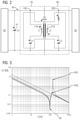
- FIG. 3 shows the impedance profile of the intermediate circuit in the exemplary embodiment according to FIG. 2 .
- FIG. 1 shows a rail vehicle 10 which is connected to an external energy supply network 12 via a pantograph 11 .
- the external energy supply network 12 provides an AC voltage at a predefined supply frequency fs of 50 Hz or 162 ⁇ 3 Hz, for example.
- the rail vehicle 10 has a rectifier 20 which is coupled to the pantograph 11 and therefore to the external energy supply network 12 .
- An inverter 30 is arranged downstream of the rectifier 20 and is controlled in such a manner that it generates a single-phase or multiphase AC voltage at the desired output frequency on the output side.
- An electrical intermediate circuit 40 comprising an intermediate circuit capacitor 41 with a capacitance Cz, an absorption circuit 50 connected in parallel and a damping absorption circuit 60 connected in parallel is situated between the rectifier 20 and the inverter 30 .
- the absorption circuit 50 and the damping absorption circuit 60 are inductively coupled to one another.
- the rectifier 20 , the inverter 30 and the electrical intermediate circuit 40 comprising the intermediate circuit capacitor 41 , the absorption circuit 50 and the damping absorption circuit 60 form a converter arrangement 13 , in which the rectifier 20 and the inverter 30 can be controlled in pulsed operation by a control device 70 belonging to the converter arrangement or by an external control device and form a pulse-controlled converter.
- the absorption circuit 50 has a series resonance at a series resonant frequency corresponding to twice the supply frequency fs of the external energy supply network 12 .
- the series resonant frequency is therefore 331 ⁇ 3 Hz and, in the case of a supply frequency fs of 50 Hz, it is 100 Hz.
- the absorption circuit 50 has a low impedance at series resonance or at twice the supply frequency fs, with the result that the first harmonic which is generated by the rectifier 20 during rectification and is at twice the supply frequency fs is short-circuited in the intermediate circuit 40 .
- the absorption circuit 50 also forms, with the intermediate circuit capacitor 41 , a parallel resonant circuit, the parallel resonant frequency of which is greater than the series resonant frequency or exceeds twice the supply frequency.
- the absorption circuit 50 has a high impedance at the parallel resonant frequency.
- the parallel resonance of the absorption circuit 50 is damped by the damping absorption circuit 60 .
- the damping absorption circuit 60 preferably has at least one non-reactive resistor which interacts with the absorption circuit 50 by means of magnetic or inductive coupling and damps the parallel resonance.
- FIG. 2 shows an exemplary embodiment of the intermediate circuit 40 according to FIG. 1 more specifically in detail.
- the intermediate circuit capacitor 41 , the absorption circuit 50 connected in parallel and the damping absorption circuit 60 are seen.
- the absorption circuit 50 is formed by a series circuit, called first series circuit 100 below, comprising an inductor 110 and a capacitance C 1 , called first capacitance below.
- the inductance L 1 of the inductor 110 and the capacitance C 1 are such that the first series circuit 100 has a low impedance at twice the supply frequency fs. This is the case if:
- f 1 denotes the series resonant frequency of the first series circuit 100 or of the absorption circuit 50 and fs denotes the supply frequency of the external energy supply network 12 .
- the first harmonic which is generated by the rectifier 20 during rectification and the frequency of which is twice the supply frequency f 1 is therefore short-circuited by the absorption circuit 50 .
- the damping absorption circuit 60 is formed by a series circuit, called second series circuit 200 below, comprising a non-reactive resistor R, a winding 210 and a capacitance C 2 , called second capacitance below.
- the winding 210 of the second series circuit 200 or of the damping absorption circuit 60 is magnetically coupled to the inductor 110 of the first series circuit or of the absorption circuit 50 ; the coupling inductance is indicated using the reference sign M.
- the first series circuit 100 has a high impedance, with the result that the voltage dropped across the inductor 110 is transformed by the winding 210 to the second series circuit 200 and therefore to the damping absorption circuit 60 , as a result of which the resistor R of the damping absorption circuit 60 in turn damps the parallel resonance of the absorption circuit 50 .
- the parallel resonant frequency f 2 results from the inductance L 1 of the inductor 110 , the first capacitance C 1 and the capacitance Cz of the intermediate circuit capacitor 41 as follows:
- the capacitance C 2 is used primarily to block direct current through the damping absorption circuit 60 .
- the following preferably applies to the inductance of the winding 210 : 0.5 ⁇ L 1 ⁇ L 2 ⁇ 0.8 ⁇ L 1 where L 1 denotes the inductance of the inductor 110 and L 2 denotes the inductance L 2 of the winding 210 .
- the following preferably applies to the magnetic coupling between the inductor 110 and the winding 210 : 0.1 ⁇ L 2 ⁇ M ⁇ 0.7 ⁇ L 2 where M denotes the coupling inductance between the inductor 110 and the winding 210 .
- FIG. 3 shows, by way of example, the impedance profile of an intermediate circuit 40 which is designed for a supply frequency of 50 Hz and in which the absorption circuit 50 accordingly has a low impedance for a series resonance of 100 Hz (see arrow with the reference sign SR). It can be seen that the impedance of the intermediate circuit 40 becomes minimal at twice the supply frequency, that is to say at 100 Hz here.
- FIG. 3 also shows that the impedance of the intermediate circuit 40 becomes very large when the parallel resonance occurs (see arrow with the reference sign PR 1 ).
- the damping absorption circuit 60 explained is provided, the resistor R of which acts on the absorption circuit 50 by means of the magnetic or inductive coupling and damps the level of the parallel resonance when it occurs (see arrow with the reference sign PR 2 ).
- the converter arrangement 13 described above by way of example therefore operates as follows:
- the impedance of the intermediate circuit capacitor 41 is considerably less than the resistance R.
- the absorption circuit 50 is inductive.
- the intermediate circuit capacitor 41 therefore acts substantially alone.
- the converter arrangement 13 described above by way of example may have one, more or all of the following advantages:
Landscapes
- Engineering & Computer Science (AREA)
- Power Engineering (AREA)
- Computer Networks & Wireless Communication (AREA)
- Electric Propulsion And Braking For Vehicles (AREA)
- Inverter Devices (AREA)
- Rectifiers (AREA)
Abstract
Description
where R denotes the resistance of the second series circuit, C1 denotes the first capacitance and fs denotes the supply frequency.
where f1 denotes the series resonant frequency of the
0.5·C1≤C2≤1.5·C1
0.5·L1≤L2≤0.8·L1
where L1 denotes the inductance of the
0.1·L2≤M≤0.7·L2
where M denotes the coupling inductance between the
voltage drops across the inductances L1 and L2 or the
the
the impedance of the
-
- It is not necessary to curtail the performance of the
inverter 30 by the additional task of actively adjusting intermediate circuit oscillations. - Sporadically occurring excitations of the
intermediate circuit 40 will generally not result in dangerously high intermediate circuit voltages. - System perturbations can be considerably reduced by dispensing with the undesirably high impedance at the parallel resonant frequency f2.
- It is not necessary to curtail the performance of the
Claims (9)
Applications Claiming Priority (4)
| Application Number | Priority Date | Filing Date | Title |
|---|---|---|---|
| DE102017215598 | 2017-09-05 | ||
| DE102017215598.1 | 2017-09-05 | ||
| DE102017215598.1A DE102017215598A1 (en) | 2017-09-05 | 2017-09-05 | Converter arrangement |
| PCT/EP2018/071882 WO2019048186A1 (en) | 2017-09-05 | 2018-08-13 | Converter assembly |
Publications (2)
| Publication Number | Publication Date |
|---|---|
| US20210067051A1 US20210067051A1 (en) | 2021-03-04 |
| US11228253B2 true US11228253B2 (en) | 2022-01-18 |
Family
ID=63405169
Family Applications (1)
| Application Number | Title | Priority Date | Filing Date |
|---|---|---|---|
| US16/644,605 Active 2038-11-27 US11228253B2 (en) | 2017-09-05 | 2018-08-13 | Converter arrangement with reduced influence of interference frequencies |
Country Status (7)
| Country | Link |
|---|---|
| US (1) | US11228253B2 (en) |
| EP (1) | EP3659247B1 (en) |
| CN (1) | CN111434019B (en) |
| DE (1) | DE102017215598A1 (en) |
| ES (1) | ES2898848T3 (en) |
| RU (1) | RU2731499C1 (en) |
| WO (1) | WO2019048186A1 (en) |
Citations (17)
| Publication number | Priority date | Publication date | Assignee | Title |
|---|---|---|---|---|
| US4170734A (en) * | 1977-12-05 | 1979-10-09 | E M I Limited | Energy regulator |
| JPS62131757A (en) | 1985-11-29 | 1987-06-15 | Hitachi Metals Ltd | Filter circuit |
| JPH06303774A (en) | 1993-04-14 | 1994-10-28 | Mitsubishi Heavy Ind Ltd | Rectification and smoothing circuit |
| US5668708A (en) | 1996-03-13 | 1997-09-16 | Spellman High Voltage Electronics Corp. | DC power supply with reduced ripple |
| US20020113562A1 (en) * | 2000-11-29 | 2002-08-22 | Sebastian Raith | Damping of resonant peaks in an electric motor which is operated using a converter with an intermediate voltage circuit, by means of a matched impedance to ground at the motor star point, and a corresponding electric motor |
| US20020113585A1 (en) * | 2000-12-22 | 2002-08-22 | Reinhold Dillig | Frequency converter system having a damping device with a passive, static impedance for damping undesirable resonant oscillations in a tuned circuit formed by at least one input-side inductance and parasitic distributed capacitances |
| US20020117913A1 (en) * | 2000-12-22 | 2002-08-29 | Sebastian Raith | Damping of resonant peaks in an electric motor, which is operated using a converter with a voltage intermediate circuit, by increasing the losses produced in the region of critical natural frequencies |
| EP1309075A2 (en) | 2001-10-30 | 2003-05-07 | Sanyo Electric Co. Ltd | Controlling device of compressor |
| RU2210852C1 (en) | 2002-02-08 | 2003-08-20 | Ульяновский государственный технический университет | Single-phase bridge-type transistor inverter with inverse diode bridge |
| US20050073863A1 (en) * | 2003-10-01 | 2005-04-07 | General Electric Company | Ripple-current reduction for transformers |
| US20070278988A1 (en) | 2006-05-31 | 2007-12-06 | Honeywell International Inc. | Common mode filter for motor controllers |
| EP1971016A2 (en) | 2007-03-16 | 2008-09-17 | Vacon Oyj | Arrangement for the suppression of current harmonics |
| US20120098351A1 (en) * | 2010-10-22 | 2012-04-26 | Just Right Surgical | RF Generator System for Surgical Vessel Sealing |
| RU2454782C1 (en) | 2011-02-07 | 2012-06-27 | Евгений Михайлович Силкин | Frequency converter control method |
| US20150280588A1 (en) | 2014-04-01 | 2015-10-01 | Meggitt US-SCPL, Securaplane Technologies, Inc. | Power converters |
| US20170104417A1 (en) * | 2015-10-09 | 2017-04-13 | Dell Products, L.P. | Line frequency ripple reduction in a resonant converter |
| US20180083539A1 (en) * | 2016-09-21 | 2018-03-22 | Express Imaging Systems, Llc | Output ripple reduction for power converters |
Family Cites Families (5)
| Publication number | Priority date | Publication date | Assignee | Title |
|---|---|---|---|---|
| DE19547969C1 (en) * | 1995-12-22 | 1997-06-19 | Asea Brown Boveri | Electrical filter for reducing sub-harmonics or intermediate harmonics |
| CN101652015A (en) * | 2008-08-13 | 2010-02-17 | 安德鲁·鲍拜尔 | High-powder factor ballast of brightness adjustable energy-saving lamp |
| CN105874700A (en) * | 2014-01-07 | 2016-08-17 | 伏达科技 | Harmonic reduction apparatus for wireless power transfer systems |
| CN104158513B (en) * | 2014-08-13 | 2017-05-10 | 武汉理工大学 | Transformerless hybrid power filter and design method thereof |
| JP6596323B2 (en) * | 2015-12-18 | 2019-10-23 | 三菱重工業株式会社 | Converter device, drive control device, motor, and compressor |
-
2017
- 2017-09-05 DE DE102017215598.1A patent/DE102017215598A1/en not_active Withdrawn
-
2018
- 2018-08-13 ES ES18759873T patent/ES2898848T3/en active Active
- 2018-08-13 EP EP18759873.5A patent/EP3659247B1/en active Active
- 2018-08-13 CN CN201880070192.XA patent/CN111434019B/en active Active
- 2018-08-13 WO PCT/EP2018/071882 patent/WO2019048186A1/en unknown
- 2018-08-13 RU RU2020112454A patent/RU2731499C1/en active
- 2018-08-13 US US16/644,605 patent/US11228253B2/en active Active
Patent Citations (17)
| Publication number | Priority date | Publication date | Assignee | Title |
|---|---|---|---|---|
| US4170734A (en) * | 1977-12-05 | 1979-10-09 | E M I Limited | Energy regulator |
| JPS62131757A (en) | 1985-11-29 | 1987-06-15 | Hitachi Metals Ltd | Filter circuit |
| JPH06303774A (en) | 1993-04-14 | 1994-10-28 | Mitsubishi Heavy Ind Ltd | Rectification and smoothing circuit |
| US5668708A (en) | 1996-03-13 | 1997-09-16 | Spellman High Voltage Electronics Corp. | DC power supply with reduced ripple |
| US20020113562A1 (en) * | 2000-11-29 | 2002-08-22 | Sebastian Raith | Damping of resonant peaks in an electric motor which is operated using a converter with an intermediate voltage circuit, by means of a matched impedance to ground at the motor star point, and a corresponding electric motor |
| US20020113585A1 (en) * | 2000-12-22 | 2002-08-22 | Reinhold Dillig | Frequency converter system having a damping device with a passive, static impedance for damping undesirable resonant oscillations in a tuned circuit formed by at least one input-side inductance and parasitic distributed capacitances |
| US20020117913A1 (en) * | 2000-12-22 | 2002-08-29 | Sebastian Raith | Damping of resonant peaks in an electric motor, which is operated using a converter with a voltage intermediate circuit, by increasing the losses produced in the region of critical natural frequencies |
| EP1309075A2 (en) | 2001-10-30 | 2003-05-07 | Sanyo Electric Co. Ltd | Controlling device of compressor |
| RU2210852C1 (en) | 2002-02-08 | 2003-08-20 | Ульяновский государственный технический университет | Single-phase bridge-type transistor inverter with inverse diode bridge |
| US20050073863A1 (en) * | 2003-10-01 | 2005-04-07 | General Electric Company | Ripple-current reduction for transformers |
| US20070278988A1 (en) | 2006-05-31 | 2007-12-06 | Honeywell International Inc. | Common mode filter for motor controllers |
| EP1971016A2 (en) | 2007-03-16 | 2008-09-17 | Vacon Oyj | Arrangement for the suppression of current harmonics |
| US20120098351A1 (en) * | 2010-10-22 | 2012-04-26 | Just Right Surgical | RF Generator System for Surgical Vessel Sealing |
| RU2454782C1 (en) | 2011-02-07 | 2012-06-27 | Евгений Михайлович Силкин | Frequency converter control method |
| US20150280588A1 (en) | 2014-04-01 | 2015-10-01 | Meggitt US-SCPL, Securaplane Technologies, Inc. | Power converters |
| US20170104417A1 (en) * | 2015-10-09 | 2017-04-13 | Dell Products, L.P. | Line frequency ripple reduction in a resonant converter |
| US20180083539A1 (en) * | 2016-09-21 | 2018-03-22 | Express Imaging Systems, Llc | Output ripple reduction for power converters |
Non-Patent Citations (2)
| Title |
|---|
| BIN GOU ; XIAOYUN FENG ; WENSHENG SONG ; KUN HAN ; XINGLAI GE: "Analysis and compensation of beat phenomenon for railway traction drive system fed with fluctuating DC-link voltage", POWER ELECTRONICS AND MOTION CONTROL CONFERENCE (IPEMC), 2012 7TH INTERNATIONAL, IEEE, 2 June 2012 (2012-06-02), pages 654 - 659, XP032215696, ISBN: 978-1-4577-2085-7, DOI: 10.1109/IPEMC.2012.6258823 |
| Bin Gou et al.: "Analysis and Compensation of Beat Phenomenon for Railway Traction Drive System Fed with Fluctuating DC-Link Voltage", 2012 IEEE 7th International Power Electronics and Motion Control Conference—ECCE Asia, Jun. 2-5, 2012 (Jun. 2, 2012) Harbin, China, pp. 654-659, XP032215696. |
Also Published As
| Publication number | Publication date |
|---|---|
| EP3659247B1 (en) | 2021-10-06 |
| CN111434019A (en) | 2020-07-17 |
| DE102017215598A1 (en) | 2019-03-07 |
| US20210067051A1 (en) | 2021-03-04 |
| EP3659247A1 (en) | 2020-06-03 |
| ES2898848T3 (en) | 2022-03-09 |
| RU2731499C1 (en) | 2020-09-03 |
| CN111434019B (en) | 2023-09-15 |
| WO2019048186A1 (en) | 2019-03-14 |
Similar Documents
| Publication | Publication Date | Title |
|---|---|---|
| EP3248270B1 (en) | An apparatus and a method for wireless transmission of power between dc voltage sources | |
| EP2895350B1 (en) | Circuit arrangement and method of operating a circuit arrangement | |
| US20190341847A1 (en) | Insulated power source and power conversion device | |
| US9809124B2 (en) | Circuit arrangement and method of operating a circuit arrangement | |
| JP4037208B2 (en) | Filter circuit | |
| US20180269796A1 (en) | Electric power conversion device | |
| US11228253B2 (en) | Converter arrangement with reduced influence of interference frequencies | |
| KR102180384B1 (en) | Power conversion device | |
| US20160261195A1 (en) | Electric power conversion device | |
| WO2014096080A2 (en) | Circuit arrangement and method of operating a circuit arrangement | |
| JP4716967B2 (en) | Filter circuit | |
| US20020113585A1 (en) | Frequency converter system having a damping device with a passive, static impedance for damping undesirable resonant oscillations in a tuned circuit formed by at least one input-side inductance and parasitic distributed capacitances | |
| KR20180117254A (en) | Auxiliary power supply device for railroad train | |
| JP2016046819A (en) | Resonance current restriction device | |
| Woronowicz et al. | A general approach to tuning of a dual secondary winding transformer for wireless power transfer | |
| US7830112B2 (en) | Method for operating a traction converter circuit for coupling to an electric DC voltage network | |
| US11973429B2 (en) | Resonant tank circuit and method for configuring resonant tank circuit | |
| JP7257820B2 (en) | ACTIVE FILTER FOR ELECTRIC RAILWAY, CONTROL METHOD THEREOF, POWER CONVERSION DEVICE AND RAILWAY VEHICLE INCLUDING THE SAME | |
| US20160111977A1 (en) | Switching Converter | |
| JP2017184564A (en) | Power conversion device | |
| WO2021070095A1 (en) | Inductive power transfer receiver | |
| JP2020178503A (en) | Power conversion device | |
| KR20180136734A (en) | The input current ripple reduction circuit of the power factor correction circuit |
Legal Events
| Date | Code | Title | Description |
|---|---|---|---|
| FEPP | Fee payment procedure |
Free format text: ENTITY STATUS SET TO UNDISCOUNTED (ORIGINAL EVENT CODE: BIG.); ENTITY STATUS OF PATENT OWNER: LARGE ENTITY |
|
| AS | Assignment |
Owner name: SIEMENS AKTIENGESELLSCHAFT, GERMANY Free format text: ASSIGNMENT OF ASSIGNORS INTEREST;ASSIGNOR:SCHMID, ROBERT;REEL/FRAME:053811/0023 Effective date: 20200226 |
|
| AS | Assignment |
Owner name: SIEMENS MOBILITY GMBH, GERMANY Free format text: ASSIGNMENT OF ASSIGNORS INTEREST;ASSIGNOR:SIEMENS AKTIENGESELLSCHAFT;REEL/FRAME:053825/0710 Effective date: 20200306 |
|
| STPP | Information on status: patent application and granting procedure in general |
Free format text: APPLICATION DISPATCHED FROM PREEXAM, NOT YET DOCKETED |
|
| STPP | Information on status: patent application and granting procedure in general |
Free format text: DOCKETED NEW CASE - READY FOR EXAMINATION |
|
| STPP | Information on status: patent application and granting procedure in general |
Free format text: NON FINAL ACTION MAILED |
|
| STPP | Information on status: patent application and granting procedure in general |
Free format text: RESPONSE TO NON-FINAL OFFICE ACTION ENTERED AND FORWARDED TO EXAMINER |
|
| STPP | Information on status: patent application and granting procedure in general |
Free format text: NOTICE OF ALLOWANCE MAILED -- APPLICATION RECEIVED IN OFFICE OF PUBLICATIONS |
|
| STPP | Information on status: patent application and granting procedure in general |
Free format text: PUBLICATIONS -- ISSUE FEE PAYMENT RECEIVED |
|
| STPP | Information on status: patent application and granting procedure in general |
Free format text: PUBLICATIONS -- ISSUE FEE PAYMENT VERIFIED |
|
| STCF | Information on status: patent grant |
Free format text: PATENTED CASE |