US11224371B2 - Neural interface probe employing amorphous silicon carbide - Google Patents
Neural interface probe employing amorphous silicon carbide Download PDFInfo
- Publication number
- US11224371B2 US11224371B2 US16/015,878 US201816015878A US11224371B2 US 11224371 B2 US11224371 B2 US 11224371B2 US 201816015878 A US201816015878 A US 201816015878A US 11224371 B2 US11224371 B2 US 11224371B2
- Authority
- US
- United States
- Prior art keywords
- silicon carbide
- amorphous silicon
- neural interface
- neural
- probe
- Prior art date
- Legal status (The legal status is an assumption and is not a legal conclusion. Google has not performed a legal analysis and makes no representation as to the accuracy of the status listed.)
- Active, expires
Links
Images


Classifications
-
- A—HUMAN NECESSITIES
- A61—MEDICAL OR VETERINARY SCIENCE; HYGIENE
- A61B—DIAGNOSIS; SURGERY; IDENTIFICATION
- A61B5/00—Measuring for diagnostic purposes; Identification of persons
- A61B5/24—Detecting, measuring or recording bioelectric or biomagnetic signals of the body or parts thereof
-
- A—HUMAN NECESSITIES
- A61—MEDICAL OR VETERINARY SCIENCE; HYGIENE
- A61L—METHODS OR APPARATUS FOR STERILISING MATERIALS OR OBJECTS IN GENERAL; DISINFECTION, STERILISATION OR DEODORISATION OF AIR; CHEMICAL ASPECTS OF BANDAGES, DRESSINGS, ABSORBENT PADS OR SURGICAL ARTICLES; MATERIALS FOR BANDAGES, DRESSINGS, ABSORBENT PADS OR SURGICAL ARTICLES
- A61L31/00—Materials for other surgical articles, e.g. stents, stent-grafts, shunts, surgical drapes, guide wires, materials for adhesion prevention, occluding devices, surgical gloves, tissue fixation devices
- A61L31/02—Inorganic materials
- A61L31/022—Metals or alloys
-
- A—HUMAN NECESSITIES
- A61—MEDICAL OR VETERINARY SCIENCE; HYGIENE
- A61L—METHODS OR APPARATUS FOR STERILISING MATERIALS OR OBJECTS IN GENERAL; DISINFECTION, STERILISATION OR DEODORISATION OF AIR; CHEMICAL ASPECTS OF BANDAGES, DRESSINGS, ABSORBENT PADS OR SURGICAL ARTICLES; MATERIALS FOR BANDAGES, DRESSINGS, ABSORBENT PADS OR SURGICAL ARTICLES
- A61L31/00—Materials for other surgical articles, e.g. stents, stent-grafts, shunts, surgical drapes, guide wires, materials for adhesion prevention, occluding devices, surgical gloves, tissue fixation devices
- A61L31/02—Inorganic materials
- A61L31/028—Other inorganic materials not covered by A61L31/022 - A61L31/026
-
- A—HUMAN NECESSITIES
- A61—MEDICAL OR VETERINARY SCIENCE; HYGIENE
- A61L—METHODS OR APPARATUS FOR STERILISING MATERIALS OR OBJECTS IN GENERAL; DISINFECTION, STERILISATION OR DEODORISATION OF AIR; CHEMICAL ASPECTS OF BANDAGES, DRESSINGS, ABSORBENT PADS OR SURGICAL ARTICLES; MATERIALS FOR BANDAGES, DRESSINGS, ABSORBENT PADS OR SURGICAL ARTICLES
- A61L31/00—Materials for other surgical articles, e.g. stents, stent-grafts, shunts, surgical drapes, guide wires, materials for adhesion prevention, occluding devices, surgical gloves, tissue fixation devices
- A61L31/04—Macromolecular materials
- A61L31/06—Macromolecular materials obtained otherwise than by reactions only involving carbon-to-carbon unsaturated bonds
-
- A—HUMAN NECESSITIES
- A61—MEDICAL OR VETERINARY SCIENCE; HYGIENE
- A61L—METHODS OR APPARATUS FOR STERILISING MATERIALS OR OBJECTS IN GENERAL; DISINFECTION, STERILISATION OR DEODORISATION OF AIR; CHEMICAL ASPECTS OF BANDAGES, DRESSINGS, ABSORBENT PADS OR SURGICAL ARTICLES; MATERIALS FOR BANDAGES, DRESSINGS, ABSORBENT PADS OR SURGICAL ARTICLES
- A61L31/00—Materials for other surgical articles, e.g. stents, stent-grafts, shunts, surgical drapes, guide wires, materials for adhesion prevention, occluding devices, surgical gloves, tissue fixation devices
- A61L31/08—Materials for coatings
- A61L31/082—Inorganic materials
- A61L31/088—Other specific inorganic materials not covered by A61L31/084 or A61L31/086
-
- A—HUMAN NECESSITIES
- A61—MEDICAL OR VETERINARY SCIENCE; HYGIENE
- A61L—METHODS OR APPARATUS FOR STERILISING MATERIALS OR OBJECTS IN GENERAL; DISINFECTION, STERILISATION OR DEODORISATION OF AIR; CHEMICAL ASPECTS OF BANDAGES, DRESSINGS, ABSORBENT PADS OR SURGICAL ARTICLES; MATERIALS FOR BANDAGES, DRESSINGS, ABSORBENT PADS OR SURGICAL ARTICLES
- A61L31/00—Materials for other surgical articles, e.g. stents, stent-grafts, shunts, surgical drapes, guide wires, materials for adhesion prevention, occluding devices, surgical gloves, tissue fixation devices
- A61L31/08—Materials for coatings
- A61L31/10—Macromolecular materials
-
- A—HUMAN NECESSITIES
- A61—MEDICAL OR VETERINARY SCIENCE; HYGIENE
- A61L—METHODS OR APPARATUS FOR STERILISING MATERIALS OR OBJECTS IN GENERAL; DISINFECTION, STERILISATION OR DEODORISATION OF AIR; CHEMICAL ASPECTS OF BANDAGES, DRESSINGS, ABSORBENT PADS OR SURGICAL ARTICLES; MATERIALS FOR BANDAGES, DRESSINGS, ABSORBENT PADS OR SURGICAL ARTICLES
- A61L31/00—Materials for other surgical articles, e.g. stents, stent-grafts, shunts, surgical drapes, guide wires, materials for adhesion prevention, occluding devices, surgical gloves, tissue fixation devices
- A61L31/14—Materials characterised by their function or physical properties, e.g. injectable or lubricating compositions, shape-memory materials, surface modified materials
-
- C—CHEMISTRY; METALLURGY
- C08—ORGANIC MACROMOLECULAR COMPOUNDS; THEIR PREPARATION OR CHEMICAL WORKING-UP; COMPOSITIONS BASED THEREON
- C08L—COMPOSITIONS OF MACROMOLECULAR COMPOUNDS
- C08L79/00—Compositions of macromolecular compounds obtained by reactions forming in the main chain of the macromolecule a linkage containing nitrogen with or without oxygen or carbon only, not provided for in groups C08L61/00 - C08L77/00
- C08L79/04—Polycondensates having nitrogen-containing heterocyclic rings in the main chain; Polyhydrazides; Polyamide acids or similar polyimide precursors
- C08L79/08—Polyimides; Polyester-imides; Polyamide-imides; Polyamide acids or similar polyimide precursors
-
- C—CHEMISTRY; METALLURGY
- C23—COATING METALLIC MATERIAL; COATING MATERIAL WITH METALLIC MATERIAL; CHEMICAL SURFACE TREATMENT; DIFFUSION TREATMENT OF METALLIC MATERIAL; COATING BY VACUUM EVAPORATION, BY SPUTTERING, BY ION IMPLANTATION OR BY CHEMICAL VAPOUR DEPOSITION, IN GENERAL; INHIBITING CORROSION OF METALLIC MATERIAL OR INCRUSTATION IN GENERAL
- C23C—COATING METALLIC MATERIAL; COATING MATERIAL WITH METALLIC MATERIAL; SURFACE TREATMENT OF METALLIC MATERIAL BY DIFFUSION INTO THE SURFACE, BY CHEMICAL CONVERSION OR SUBSTITUTION; COATING BY VACUUM EVAPORATION, BY SPUTTERING, BY ION IMPLANTATION OR BY CHEMICAL VAPOUR DEPOSITION, IN GENERAL
- C23C16/00—Chemical coating by decomposition of gaseous compounds, without leaving reaction products of surface material in the coating, i.e. chemical vapour deposition [CVD] processes
- C23C16/22—Chemical coating by decomposition of gaseous compounds, without leaving reaction products of surface material in the coating, i.e. chemical vapour deposition [CVD] processes characterised by the deposition of inorganic material, other than metallic material
- C23C16/30—Deposition of compounds, mixtures or solid solutions, e.g. borides, carbides, nitrides
- C23C16/32—Carbides
- C23C16/325—Silicon carbide
-
- C—CHEMISTRY; METALLURGY
- C23—COATING METALLIC MATERIAL; COATING MATERIAL WITH METALLIC MATERIAL; CHEMICAL SURFACE TREATMENT; DIFFUSION TREATMENT OF METALLIC MATERIAL; COATING BY VACUUM EVAPORATION, BY SPUTTERING, BY ION IMPLANTATION OR BY CHEMICAL VAPOUR DEPOSITION, IN GENERAL; INHIBITING CORROSION OF METALLIC MATERIAL OR INCRUSTATION IN GENERAL
- C23C—COATING METALLIC MATERIAL; COATING MATERIAL WITH METALLIC MATERIAL; SURFACE TREATMENT OF METALLIC MATERIAL BY DIFFUSION INTO THE SURFACE, BY CHEMICAL CONVERSION OR SUBSTITUTION; COATING BY VACUUM EVAPORATION, BY SPUTTERING, BY ION IMPLANTATION OR BY CHEMICAL VAPOUR DEPOSITION, IN GENERAL
- C23C16/00—Chemical coating by decomposition of gaseous compounds, without leaving reaction products of surface material in the coating, i.e. chemical vapour deposition [CVD] processes
- C23C16/44—Chemical coating by decomposition of gaseous compounds, without leaving reaction products of surface material in the coating, i.e. chemical vapour deposition [CVD] processes characterised by the method of coating
- C23C16/50—Chemical coating by decomposition of gaseous compounds, without leaving reaction products of surface material in the coating, i.e. chemical vapour deposition [CVD] processes characterised by the method of coating using electric discharges
-
- C—CHEMISTRY; METALLURGY
- C23—COATING METALLIC MATERIAL; COATING MATERIAL WITH METALLIC MATERIAL; CHEMICAL SURFACE TREATMENT; DIFFUSION TREATMENT OF METALLIC MATERIAL; COATING BY VACUUM EVAPORATION, BY SPUTTERING, BY ION IMPLANTATION OR BY CHEMICAL VAPOUR DEPOSITION, IN GENERAL; INHIBITING CORROSION OF METALLIC MATERIAL OR INCRUSTATION IN GENERAL
- C23C—COATING METALLIC MATERIAL; COATING MATERIAL WITH METALLIC MATERIAL; SURFACE TREATMENT OF METALLIC MATERIAL BY DIFFUSION INTO THE SURFACE, BY CHEMICAL CONVERSION OR SUBSTITUTION; COATING BY VACUUM EVAPORATION, BY SPUTTERING, BY ION IMPLANTATION OR BY CHEMICAL VAPOUR DEPOSITION, IN GENERAL
- C23C16/00—Chemical coating by decomposition of gaseous compounds, without leaving reaction products of surface material in the coating, i.e. chemical vapour deposition [CVD] processes
- C23C16/56—After-treatment
-
- C—CHEMISTRY; METALLURGY
- C23—COATING METALLIC MATERIAL; COATING MATERIAL WITH METALLIC MATERIAL; CHEMICAL SURFACE TREATMENT; DIFFUSION TREATMENT OF METALLIC MATERIAL; COATING BY VACUUM EVAPORATION, BY SPUTTERING, BY ION IMPLANTATION OR BY CHEMICAL VAPOUR DEPOSITION, IN GENERAL; INHIBITING CORROSION OF METALLIC MATERIAL OR INCRUSTATION IN GENERAL
- C23C—COATING METALLIC MATERIAL; COATING MATERIAL WITH METALLIC MATERIAL; SURFACE TREATMENT OF METALLIC MATERIAL BY DIFFUSION INTO THE SURFACE, BY CHEMICAL CONVERSION OR SUBSTITUTION; COATING BY VACUUM EVAPORATION, BY SPUTTERING, BY ION IMPLANTATION OR BY CHEMICAL VAPOUR DEPOSITION, IN GENERAL
- C23C28/00—Coating for obtaining at least two superposed coatings either by methods not provided for in a single one of groups C23C2/00 - C23C26/00 or by combinations of methods provided for in subclasses C23C and C25C or C25D
- C23C28/30—Coatings combining at least one metallic layer and at least one inorganic non-metallic layer
- C23C28/32—Coatings combining at least one metallic layer and at least one inorganic non-metallic layer including at least one pure metallic layer
-
- C—CHEMISTRY; METALLURGY
- C23—COATING METALLIC MATERIAL; COATING MATERIAL WITH METALLIC MATERIAL; CHEMICAL SURFACE TREATMENT; DIFFUSION TREATMENT OF METALLIC MATERIAL; COATING BY VACUUM EVAPORATION, BY SPUTTERING, BY ION IMPLANTATION OR BY CHEMICAL VAPOUR DEPOSITION, IN GENERAL; INHIBITING CORROSION OF METALLIC MATERIAL OR INCRUSTATION IN GENERAL
- C23C—COATING METALLIC MATERIAL; COATING MATERIAL WITH METALLIC MATERIAL; SURFACE TREATMENT OF METALLIC MATERIAL BY DIFFUSION INTO THE SURFACE, BY CHEMICAL CONVERSION OR SUBSTITUTION; COATING BY VACUUM EVAPORATION, BY SPUTTERING, BY ION IMPLANTATION OR BY CHEMICAL VAPOUR DEPOSITION, IN GENERAL
- C23C28/00—Coating for obtaining at least two superposed coatings either by methods not provided for in a single one of groups C23C2/00 - C23C26/00 or by combinations of methods provided for in subclasses C23C and C25C or C25D
- C23C28/30—Coatings combining at least one metallic layer and at least one inorganic non-metallic layer
- C23C28/34—Coatings combining at least one metallic layer and at least one inorganic non-metallic layer including at least one inorganic non-metallic material layer, e.g. metal carbide, nitride, boride, silicide layer and their mixtures, enamels, phosphates and sulphates
- C23C28/341—Coatings combining at least one metallic layer and at least one inorganic non-metallic layer including at least one inorganic non-metallic material layer, e.g. metal carbide, nitride, boride, silicide layer and their mixtures, enamels, phosphates and sulphates with at least one carbide layer
-
- A—HUMAN NECESSITIES
- A61—MEDICAL OR VETERINARY SCIENCE; HYGIENE
- A61B—DIAGNOSIS; SURGERY; IDENTIFICATION
- A61B2562/00—Details of sensors; Constructional details of sensor housings or probes; Accessories for sensors
- A61B2562/02—Details of sensors specially adapted for in-vivo measurements
- A61B2562/0209—Special features of electrodes classified in A61B5/24, A61B5/25, A61B5/283, A61B5/291, A61B5/296, A61B5/053
-
- A—HUMAN NECESSITIES
- A61—MEDICAL OR VETERINARY SCIENCE; HYGIENE
- A61B—DIAGNOSIS; SURGERY; IDENTIFICATION
- A61B2562/00—Details of sensors; Constructional details of sensor housings or probes; Accessories for sensors
- A61B2562/04—Arrangements of multiple sensors of the same type
- A61B2562/043—Arrangements of multiple sensors of the same type in a linear array
-
- A—HUMAN NECESSITIES
- A61—MEDICAL OR VETERINARY SCIENCE; HYGIENE
- A61B—DIAGNOSIS; SURGERY; IDENTIFICATION
- A61B2562/00—Details of sensors; Constructional details of sensor housings or probes; Accessories for sensors
- A61B2562/12—Manufacturing methods specially adapted for producing sensors for in-vivo measurements
- A61B2562/125—Manufacturing methods specially adapted for producing sensors for in-vivo measurements characterised by the manufacture of electrodes
-
- A—HUMAN NECESSITIES
- A61—MEDICAL OR VETERINARY SCIENCE; HYGIENE
- A61B—DIAGNOSIS; SURGERY; IDENTIFICATION
- A61B5/00—Measuring for diagnostic purposes; Identification of persons
- A61B5/24—Detecting, measuring or recording bioelectric or biomagnetic signals of the body or parts thereof
- A61B5/25—Bioelectric electrodes therefor
- A61B5/279—Bioelectric electrodes therefor specially adapted for particular uses
- A61B5/291—Bioelectric electrodes therefor specially adapted for particular uses for electroencephalography [EEG]
-
- A—HUMAN NECESSITIES
- A61—MEDICAL OR VETERINARY SCIENCE; HYGIENE
- A61B—DIAGNOSIS; SURGERY; IDENTIFICATION
- A61B5/00—Measuring for diagnostic purposes; Identification of persons
- A61B5/68—Arrangements of detecting, measuring or recording means, e.g. sensors, in relation to patient
- A61B5/6846—Arrangements of detecting, measuring or recording means, e.g. sensors, in relation to patient specially adapted to be brought in contact with an internal body part, i.e. invasive
- A61B5/6867—Arrangements of detecting, measuring or recording means, e.g. sensors, in relation to patient specially adapted to be brought in contact with an internal body part, i.e. invasive specially adapted to be attached or implanted in a specific body part
- A61B5/6868—Brain
Definitions
- One embodiment of the invention is a neural interface device that comprises an implantable microelectrode body.
- the implantable microelectrode body includes a neural interface probe, which includes a thin film metal trace connected to an interface pad and an amorphous silicon carbide insulation.
- the amorphous silicon carbide insulation surrounds the thin film metal trace to form an outside surface of the neural interface probe.
- the interface pad is exposed to an ambient environment of the neural interface probe through an opening in the amorphous silicon carbide insulation.
- the plasma enhanced chemical vapor deposition conditions of the first and second amorphous silicon carbide insulation layers and the formation conditions of the thin film metal trace and the interface pad can be selected such that intrinsic stresses in the first and second amorphous silicon carbide insulation layers are offset by residual stresses in the thin film metal trace and the interface pad, such that the neural interface probe has a substantially neutral stress.
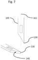
- FIG. 5 is an embodiment of the implantable microelectrode body ( 100 ) comprising six neural interface probes ( 105 ) in contact with a connection body ( 120 ) wherein the neural interface probes are configured to have more than one length, each neural interface probe optionally having a neural interface pad ( 115 ) defined by an opening in an a-SiC layer ( 135 );
- FIG. 17 is an optical photograph of an example embodiment of an implantable microelectrode body showing a separation between neural interface probes ( 105 ) and a connection body ( 120 );
- the neural interface devices of the present invention employ amorphous silicon carbide.
- Amorphous silicon carbide is distinguished from other forms of silicon carbide by not exhibiting crystallinity when analyzed by x-ray diffraction.
- Prior art devices discloses the use of polycrystalline silicon carbide in the construction of devices intended for interfacing to neural tissue.
- Diaz-Botia et al., 2017 teach the use of crystalline silicon carbide in a geometry that disposes electrode sites in a planar configuration on the surface of a neural tissue target.
- Polycrystalline silicon carbide is formed at high temperatures by low pressure chemical vapor deposition and is n-doped and consequently has electronic conductivity.
- h is desirably less than 10 micrometers.
- An advantage of the rectangular cross-section compared with the circular cross-section employed in Prior Art carbon fiber electrodes is the higher area moment of inertia of the rectangular cross-section for the same minimum cross-sectional dimension.
- a circular neural probe with an equivalent minimum cross-sectional dimension has an area moment of inertia of 31 ⁇ m 4 .
- the area moment of inertia of the rectangular cross-section is higher, imparting the desirable property of increased buckling resistance.
- the rectangular probe has a minimum cross-sectional dimension that is less than or equal to 88% that of the circular probe.
- the smaller cross-sectional dimension of the rectangular probe advantageously reduces the foreign body response.
- the foregoing discussion teaches an advantage of a neural probe with a rectangular cross section for increasing buckling resistance while minimizing tissue damage.
- a further increase in buckling resistance is obtained by configuring the cross-section of the probe to comprise substantially of a high-elastic-modulus material.
- a further advantage is obtained if the high elastic modulus material is disposed on the perimeter of the probe cross-section.
- the present invention is directed to the use of amorphous silicon carbide as the high elastic modulus material.
- Amorphous silicon carbide has a modulus of elasticity of approximately 300 GPa. Skilled artisans will appreciate that the modulus may vary depending on the method and process parameters used in the preparation of the amorphous silicon carbide.
- the cross-sectional dimensions of an interface probe having a multiplicity of metal traces may be increased to achieve a desired EI product while preserving the constraints that at least one cross-sectional probe dimension is less than 10 ⁇ m and the EI product is 15.6 N- ⁇ m 2 or greater.
- a useful feature of the neural interface probe of the present invention is a high degree of planarity.
- Planarity is the property of the neural interface probe that the upper and lower surfaces of the probe are co-planar and that each of these surfaces lie within a plane.
- the planarity of the probe is advantageous in minimizing tissue damage during implantation. It is commonly understood that thin films of materials fabricated by the processes employed in the fabrication of the neural interface probes have intrinsic residual stresses. If these stresses are unbalanced or non-uniformly distributed within the neural interface probe, a deflection of the probe occurs with consequent loss of planarity. In amorphous silicon carbide these residual stresses are typically compressive. Carefully selection of deposition conditions for the formation of the amorphous silicon carbide is required to minimize these stresses.
- one or more of the plurality of neural interface probes ( 105 ) is configured without a neural interface pad.
- Neural interface probes without a neural interface pad are desirable for the purpose of stabilizing an implantable microelectrode body on the surface of the implanted tissue.
- the neural interface probes when an implantable microelectrode body with a plurality of neural interface probes is withdrawn from water, the neural interface probes form a bundle in which the neural interface probes are weakly held together by van der Waals bonding.
- the bundle has a higher stiffness than an individual neural probe allowing penetration of the probe bundle into tissue during implantation without buckling of the bundle.
- Gardner et al U.S. application Ser. No. 14/902,734
- the individual neural probes within a bundle will splay into tissue during implantation causing the interface pads to be distributed advantageously in a three-dimensional volume of tissue.
- a similar bundling and splaying behavior has been observed with amorphous silicon carbide neural interface probes.
- amorphous silicon carbide probes with intrinsic curvature will also form a bundle weakly held together by van der Waals bonding.
- the intrinsic curvature of the amorphous silicon carbide is advantageous in promoting splaying of the neural probes as they traverse tissue during implantation.
- a shortcoming of Prior Art implantable devices based on carbon fiber electrodes is the inability to fabricate neural probes from carbon fiber having intrinsic curvature.
- a neural interface probe is configured to have a plurality of interface pads.
- a plan view of a neural interface probe ( 105 ) of the present embodiment having four interface pads ( 115 ) is shown in FIG. 9 .
- Each interface pad ( 115 ) may be in contact with a metal trace also in contact with the amorphous silicon carbide insulation.
- Each interface pad may be connected to the ambient through an opening in the amorphous silicon carbide insulation.
- thin film metal traces of the neural interface probe can extend to a communication circuit of the connection body ( 120 ), and, the communication circuit can include an electrical contact pad directly connected to the thin film metal trace.
- a perpendicular cross-sectional view of a neural interface probe of the present embodiment having four interface pads is shown in FIG. 10 .
- the number of interface pads on a neural interface probe may be in the range two to 16.
- Such advantages may include, without limitation, the ability to use large telemetry devices on the connection body without interfering with the function of the neural tissue or the ability to place the communication circuitry outside the body without the use of a telemetry device or without the need for implanted electrical connections between a wire or ribbon cable and the communication circuitry.
- a plurality of neural interface devices ( 100 ) are configured in a parallel orientation with the connection bodies ( 120 ) of the neural interface devices in a face-to-face orientation.
- the connection bodies of the interface devices are separated by a solid spacer ( 195 ).
- the contacting surfaces of the spacer ( 195 ) and the connection bodies ( 120 ) are adhesively bonded with an epoxy, acrylic, or other bonding agent suitable for chronic implantation.
- a first layer of amorphous silicon carbide ( 160 ) having a thickness of about 2 microns is then deposited over the polyimide layer by plasma enhanced chemical vapor deposition (PECVD) at a substrate temperature of 325° C., RF power density of 0.20 Wcm ⁇ 2 (13.56 MHz), and pressure of 1000 millitorr using a reactive gas mixture of silane (SiH 4 ) and methane (CH 4 ) at flow rates of 12 sccm and 36 sccm respectively.
- the total gas flow rate into the PECVD reaction chamber is maintained at 800 sccm using argon as a carrier gas.
- thin film metal traces are formed on the first amorphous silicon layer by sputter deposition using lift-off photolithography to define the metal pattern.
- a non-photosensitive resist layer known as lift off resist and a photosensitive resist layer are spin-coated consecutively on the first amorphous silicon carbide layer in a process designed to create an undercut in the two-layer resist.
- the two-layer resist is then exposed to ultraviolet radiation through a first photomask that defines the pattern of the metal traces on the neural interface probe and on the connection body of the device.
- FIG. 17 An optical image of an implantable microelectrode of Example 1 is shown in FIG. 17 .
- the microelectrode comprises eight neural interface probes ( 105 ) connected to a connection body ( 120 ).
- the distal tip of each neural interface probe terminates in a symmetric triangular tip with an included angle of 10 to 14 degrees.
- Each neural interface probe has a thin metal trace ( 110 ) that extends from an interface pad near the distal tip of the neural probe to an electrical contact pad on the connection body.
Abstract
Description
Claims (21)
Priority Applications (2)
| Application Number | Priority Date | Filing Date | Title |
|---|---|---|---|
| US16/015,878 US11224371B2 (en) | 2017-06-23 | 2018-06-22 | Neural interface probe employing amorphous silicon carbide |
| US17/559,835 US20220110565A1 (en) | 2017-06-23 | 2021-12-22 | Method of manufacturing a neural interface probe employing amorphous silicon carbide |
Applications Claiming Priority (2)
| Application Number | Priority Date | Filing Date | Title |
|---|---|---|---|
| US201762523825P | 2017-06-23 | 2017-06-23 | |
| US16/015,878 US11224371B2 (en) | 2017-06-23 | 2018-06-22 | Neural interface probe employing amorphous silicon carbide |
Related Child Applications (1)
| Application Number | Title | Priority Date | Filing Date |
|---|---|---|---|
| US17/559,835 Division US20220110565A1 (en) | 2017-06-23 | 2021-12-22 | Method of manufacturing a neural interface probe employing amorphous silicon carbide |
Publications (2)
| Publication Number | Publication Date |
|---|---|
| US20180368712A1 US20180368712A1 (en) | 2018-12-27 |
| US11224371B2 true US11224371B2 (en) | 2022-01-18 |
Family
ID=64691617
Family Applications (2)
| Application Number | Title | Priority Date | Filing Date |
|---|---|---|---|
| US16/015,878 Active 2039-10-27 US11224371B2 (en) | 2017-06-23 | 2018-06-22 | Neural interface probe employing amorphous silicon carbide |
| US17/559,835 Pending US20220110565A1 (en) | 2017-06-23 | 2021-12-22 | Method of manufacturing a neural interface probe employing amorphous silicon carbide |
Family Applications After (1)
| Application Number | Title | Priority Date | Filing Date |
|---|---|---|---|
| US17/559,835 Pending US20220110565A1 (en) | 2017-06-23 | 2021-12-22 | Method of manufacturing a neural interface probe employing amorphous silicon carbide |
Country Status (1)
| Country | Link |
|---|---|
| US (2) | US11224371B2 (en) |
Families Citing this family (6)
| Publication number | Priority date | Publication date | Assignee | Title |
|---|---|---|---|---|
| US20200303236A1 (en) * | 2017-09-27 | 2020-09-24 | Board Of Trustees Of Michigan State University | Implantable all diamond microelectrode and fabrication method |
| EP3890608A4 (en) * | 2018-12-03 | 2022-08-24 | Laxmi Therapeutic Devices, Inc. | Needles for measurement of body fluid analytes such as glucose |
| US11596787B2 (en) * | 2019-03-28 | 2023-03-07 | Board Of Regents, The University Of Texas System | Peripheral nerve electrode for neural recording and stimulation |
| CN114014252A (en) * | 2021-11-02 | 2022-02-08 | 杭州电子科技大学温州研究院有限公司 | High-density low-noise rigid-flexible combined nerve probe and preparation method thereof |
| CN115429282B (en) * | 2022-07-25 | 2024-02-06 | 武汉衷华脑机融合科技发展有限公司 | Composite microneedle structure and nerve microelectrode |
| CN115500832B (en) * | 2022-08-24 | 2024-04-02 | 武汉衷华脑机融合科技发展有限公司 | Composite microneedle structure |
Citations (11)
| Publication number | Priority date | Publication date | Assignee | Title |
|---|---|---|---|---|
| US5755759A (en) * | 1996-03-14 | 1998-05-26 | Eic Laboratories, Inc. | Biomedical device with a protective overlayer |
| US20070219551A1 (en) * | 2003-09-22 | 2007-09-20 | Honour Kirk S | Medical device with flexible printed circuit |
| US20100198297A1 (en) * | 2009-01-15 | 2010-08-05 | Cogan Stuart F | Wireless Recording and Stimulation of Brain Activity |
| US20110288391A1 (en) * | 2010-05-19 | 2011-11-24 | Purdue Research Foundation | Titanium-Based Multi-Channel Microelectrode Array for Electrophysiological Recording and Stimulation of Neural Tissue |
| WO2013010161A2 (en) | 2011-07-14 | 2013-01-17 | University Of South Florida | Long-term implantable silicon carbide neural interface device using the electrical field effect |
| US20130345780A1 (en) * | 2012-06-19 | 2013-12-26 | Phillipe J. Tabada | Conformally Encapsulated Multi-Electrode Arrays With Seamless Insulation |
| US8738110B2 (en) * | 2009-05-01 | 2014-05-27 | Livermore National Security, Llc | Rigid spine reinforced polymer microelectrode array probe and method of fabrication |
| WO2015003185A2 (en) | 2013-07-05 | 2015-01-08 | Trustees Of Boston University | Minimally invasive splaying microfiber electrode array and methods of fabricating and implanting the same |
| US9211401B2 (en) * | 2009-11-30 | 2015-12-15 | University Of South Florida | Cubic silicon carbide implantable neural prosthetic |
| US20160220135A1 (en) * | 2013-09-13 | 2016-08-04 | University Of Utah Research Foundation | Micro-molded electrodes, arrays, and methods of making the same |
| US9844660B2 (en) * | 2013-11-08 | 2017-12-19 | Neuronexus Technologies, Inc. | Three-dimensional neural probe microelectrode array and method of manufacture |
-
2018
- 2018-06-22 US US16/015,878 patent/US11224371B2/en active Active
-
2021
- 2021-12-22 US US17/559,835 patent/US20220110565A1/en active Pending
Patent Citations (13)
| Publication number | Priority date | Publication date | Assignee | Title |
|---|---|---|---|---|
| US5755759A (en) * | 1996-03-14 | 1998-05-26 | Eic Laboratories, Inc. | Biomedical device with a protective overlayer |
| US20070219551A1 (en) * | 2003-09-22 | 2007-09-20 | Honour Kirk S | Medical device with flexible printed circuit |
| US20100198297A1 (en) * | 2009-01-15 | 2010-08-05 | Cogan Stuart F | Wireless Recording and Stimulation of Brain Activity |
| US8738110B2 (en) * | 2009-05-01 | 2014-05-27 | Livermore National Security, Llc | Rigid spine reinforced polymer microelectrode array probe and method of fabrication |
| US9211401B2 (en) * | 2009-11-30 | 2015-12-15 | University Of South Florida | Cubic silicon carbide implantable neural prosthetic |
| US20110288391A1 (en) * | 2010-05-19 | 2011-11-24 | Purdue Research Foundation | Titanium-Based Multi-Channel Microelectrode Array for Electrophysiological Recording and Stimulation of Neural Tissue |
| WO2013010161A2 (en) | 2011-07-14 | 2013-01-17 | University Of South Florida | Long-term implantable silicon carbide neural interface device using the electrical field effect |
| US10136825B2 (en) * | 2011-07-14 | 2018-11-27 | University Of South Florida | Long-term implantable silicon carbide neural interface device using the electrical field effect |
| US20130345780A1 (en) * | 2012-06-19 | 2013-12-26 | Phillipe J. Tabada | Conformally Encapsulated Multi-Electrode Arrays With Seamless Insulation |
| US9498617B2 (en) * | 2012-06-19 | 2016-11-22 | Lawrence Livermore National Security, Llc | Conformally encapsulated multi-electrode arrays with seamless insulation |
| WO2015003185A2 (en) | 2013-07-05 | 2015-01-08 | Trustees Of Boston University | Minimally invasive splaying microfiber electrode array and methods of fabricating and implanting the same |
| US20160220135A1 (en) * | 2013-09-13 | 2016-08-04 | University Of Utah Research Foundation | Micro-molded electrodes, arrays, and methods of making the same |
| US9844660B2 (en) * | 2013-11-08 | 2017-12-19 | Neuronexus Technologies, Inc. | Three-dimensional neural probe microelectrode array and method of manufacture |
Non-Patent Citations (10)
| Title |
|---|
| Azevedo, et al.; "Silicon Carbide Coated Mems Strain Sensor for Harsh Environment Applications"; Proceedings of the IEEE International Conference on Micro Electro Mechanical Systems (MEMS) dio:10.1109/MEMSYS.2007.4433166; Feb. 2007; 4 pgs. |
| Cogan, et al.; "Plasma-enhanced chemical vapor deposited silicon carbide as an implantable dielectric coating"; Wiley Periodicals, Inc.; 2003; pp. 856-867. |
| Diaz-Botia, et al.; "A silicon carbide array for electrocorticography and peripheral nerve recording"; Open Access; IOP Publishing; Journal of Neural Engineering; 14 056006; https://doi.org/10.1088/1741-2552/aa7698; 2017; 11 pgs. |
| Frewin, et al.; "Models and Stimulation Paradigms—Electrical Performance of Single Material Silicon Carbide (SiC) Microelectrodes" A Joint Meeting of NANS & NIC; Jun. 25-29, 2016; 1 pg. |
| Frewin, et al.; "Sensory Motor Integration—Electrochemical Evaluation of Shape Memory Polymer Electrodes"; A Joint Meeting of NANA & NIC; Jun. 25-29, 2016; 1 pg. |
| Hsu, et al.; "Characterization of a Sicx:H thin films as an encapsulation material for integrated silicon based neural interface devices"; NIH Public Access—Author Manuscript—Thin Solid Films; Nov. 1, 2007; pp. 1-24. |
| Kalnins, et al.; "Clinical outcomes of silicon carbide coated stents in patients with coronary artery disease"; http://www.MedSciMonit.com/pub/vol_8/no_2/1900.pdf; Product Investigation; PMID: 11859292; 2002; pages PI16-PI20. |
| Knaack, et al.; "In vivo Characterization of Amorphous Silicon Carbide As a Biomaterial for Chronic Neural Interfaces" Frontiers in Neuroscience; vol. 10 | Article 301; doi: 10.3389/fnins.2016.00301; Jun. 28, 2016; 12 pgs. |
| Lei, et al.; "SiC protective coating for photovoltaic retinal prosthesis"; IOP Publishing; Journal of Neural Engineering; 13 046016; doi:10.1088/1741-2560/13/4/046016; 2016; 12 pgs. |
| Zorman; "Silico Carbide as a Material for Biomedical Microsystems"; HAL archives-ouvertes.fr; EDA Publishing Association, pp. 7, 2009, <hal-00395712>; https://hal.archives-ouvertes.fr/hal-00395712; Jun. 16, 2009; 8 pgs. |
Also Published As
| Publication number | Publication date |
|---|---|
| US20180368712A1 (en) | 2018-12-27 |
| US20220110565A1 (en) | 2022-04-14 |
Similar Documents
| Publication | Publication Date | Title |
|---|---|---|
| US20220110565A1 (en) | Method of manufacturing a neural interface probe employing amorphous silicon carbide | |
| US8170638B2 (en) | MEMS flexible substrate neural probe and method of fabricating same | |
| US6829498B2 (en) | Device for creating a neural interface and method for making same | |
| US7790493B2 (en) | Wafer-level, polymer-based encapsulation for microstructure devices | |
| US8271099B1 (en) | Implantable paddle lead comprising compressive longitudinal members for supporting electrodes and method of fabrication | |
| US9020608B2 (en) | Implantable paddle lead comprising stretching electrical traces and method of fabrication | |
| EP2393551A2 (en) | Multiplexed multi-electrode neurostimulation devices with integrated circuit having integrated electrodes | |
| US20160324435A1 (en) | Graphene-passivated implantable electrodes | |
| KR101616294B1 (en) | Hybrid type microelectrode array and fabrication method thereof | |
| WO2012114501A1 (en) | Brain probe and method for manufacturing same | |
| US10856764B2 (en) | Method for forming a multielectrode conformal penetrating array | |
| US11401620B2 (en) | Method of producing patterned microwire bundles | |
| JPH01287606A (en) | Fine adjustment mechanism of scanning tunnel microscope | |
| CN113015552A (en) | Branch proximal connector for high density neural interface | |
| KR20220113405A (en) | Implantable Stimulator with Electrode Array and Compliant Substrate | |
| KR101503391B1 (en) | Electrode for measuring neural signal including single-crystalline au nanowire | |
| US20190254546A1 (en) | Neural multielectrode arrays and their manufacture and use | |
| CN114098740A (en) | Micro-needle | |
| KR100489377B1 (en) | Neural Probe Arrays with Arbitrary Shape and Methods of Fabricating the Same | |
| Perlin et al. | The effect of the substrate on the extracellular neural activity recorded micromachined silicon microprobes | |
| US11785716B2 (en) | Implantable electrical connecting device | |
| EP4054704A1 (en) | Anatomically contoured stimulation leads for high density neural interface | |
| KR102583257B1 (en) | Electrode structure for neuromodulation device | |
| KR20210060273A (en) | A neural electrode arrangement and method for manufacturing the same | |
| WO2022258818A1 (en) | Electrode device |
Legal Events
| Date | Code | Title | Description |
|---|---|---|---|
| FEPP | Fee payment procedure |
Free format text: ENTITY STATUS SET TO UNDISCOUNTED (ORIGINAL EVENT CODE: BIG.); ENTITY STATUS OF PATENT OWNER: SMALL ENTITY |
|
| FEPP | Fee payment procedure |
Free format text: ENTITY STATUS SET TO SMALL (ORIGINAL EVENT CODE: SMAL); ENTITY STATUS OF PATENT OWNER: SMALL ENTITY |
|
| AS | Assignment |
Owner name: BOARD OF REGENTS, THE UNIVERSITY OF TEXAS SYSTEM, TEXAS Free format text: ASSIGNMENT OF ASSIGNORS INTEREST;ASSIGNOR:COGAN, STUART F.;REEL/FRAME:047374/0233 Effective date: 20180629 Owner name: TRUSTEES OF BOSTON UNIVERSITY, MASSACHUSETTS Free format text: ASSIGNMENT OF ASSIGNORS INTEREST;ASSIGNOR:GARDNER, TIMOTHY JAMES;REEL/FRAME:047374/0205 Effective date: 20181029 Owner name: BOARD OF REGENTS, THE UNIVERSITY OF TEXAS SYSTEM, Free format text: ASSIGNMENT OF ASSIGNORS INTEREST;ASSIGNOR:COGAN, STUART F.;REEL/FRAME:047374/0233 Effective date: 20180629 |
|
| STPP | Information on status: patent application and granting procedure in general |
Free format text: DOCKETED NEW CASE - READY FOR EXAMINATION |
|
| STPP | Information on status: patent application and granting procedure in general |
Free format text: NON FINAL ACTION MAILED |
|
| STPP | Information on status: patent application and granting procedure in general |
Free format text: RESPONSE TO NON-FINAL OFFICE ACTION ENTERED AND FORWARDED TO EXAMINER |
|
| STPP | Information on status: patent application and granting procedure in general |
Free format text: NOTICE OF ALLOWANCE MAILED -- APPLICATION RECEIVED IN OFFICE OF PUBLICATIONS |
|
| STPP | Information on status: patent application and granting procedure in general |
Free format text: PUBLICATIONS -- ISSUE FEE PAYMENT VERIFIED |
|
| STCF | Information on status: patent grant |
Free format text: PATENTED CASE |