US10965126B2 - Systems and methods for control of photovoltaic arrays - Google Patents
Systems and methods for control of photovoltaic arrays Download PDFInfo
- Publication number
- US10965126B2 US10965126B2 US15/583,456 US201715583456A US10965126B2 US 10965126 B2 US10965126 B2 US 10965126B2 US 201715583456 A US201715583456 A US 201715583456A US 10965126 B2 US10965126 B2 US 10965126B2
- Authority
- US
- United States
- Prior art keywords
- voltage
- bus
- output
- power
- module
- Prior art date
- Legal status (The legal status is an assumption and is not a legal conclusion. Google has not performed a legal analysis and makes no representation as to the accuracy of the status listed.)
- Active, expires
Links
- 238000000034 method Methods 0.000 title claims description 10
- 238000003491 array Methods 0.000 title description 3
- 238000001514 detection method Methods 0.000 claims abstract description 31
- 230000006854 communication Effects 0.000 claims description 88
- 238000004891 communication Methods 0.000 claims description 88
- 230000004044 response Effects 0.000 claims description 39
- 230000008859 change Effects 0.000 claims description 10
- 238000006243 chemical reaction Methods 0.000 claims description 8
- 238000011144 upstream manufacturing Methods 0.000 claims description 4
- 238000005070 sampling Methods 0.000 claims description 3
- 230000007175 bidirectional communication Effects 0.000 claims 1
- 230000001052 transient effect Effects 0.000 description 16
- FUYLLJCBCKRIAL-UHFFFAOYSA-N 4-methylumbelliferone sulfate Chemical compound C1=C(OS(O)(=O)=O)C=CC2=C1OC(=O)C=C2C FUYLLJCBCKRIAL-UHFFFAOYSA-N 0.000 description 13
- 238000007726 management method Methods 0.000 description 13
- 230000001276 controlling effect Effects 0.000 description 7
- 238000012986 modification Methods 0.000 description 7
- 230000004048 modification Effects 0.000 description 7
- 238000005516 engineering process Methods 0.000 description 6
- 239000004020 conductor Substances 0.000 description 5
- 230000006870 function Effects 0.000 description 5
- 230000003287 optical effect Effects 0.000 description 4
- 239000003990 capacitor Substances 0.000 description 3
- 238000013459 approach Methods 0.000 description 2
- 238000010586 diagram Methods 0.000 description 2
- 238000007599 discharging Methods 0.000 description 2
- 239000000835 fiber Substances 0.000 description 2
- 230000002093 peripheral effect Effects 0.000 description 2
- 238000004549 pulsed laser deposition Methods 0.000 description 2
- 230000001105 regulatory effect Effects 0.000 description 2
- 238000001429 visible spectrum Methods 0.000 description 2
- 230000008901 benefit Effects 0.000 description 1
- 238000004590 computer program Methods 0.000 description 1
- 230000001419 dependent effect Effects 0.000 description 1
- 230000005611 electricity Effects 0.000 description 1
- 238000002955 isolation Methods 0.000 description 1
- 238000005259 measurement Methods 0.000 description 1
- 239000002184 metal Substances 0.000 description 1
- 238000012913 prioritisation Methods 0.000 description 1
- 230000005855 radiation Effects 0.000 description 1
- 230000009467 reduction Effects 0.000 description 1
- 238000012546 transfer Methods 0.000 description 1
- 230000007723 transport mechanism Effects 0.000 description 1
- 230000001960 triggered effect Effects 0.000 description 1
Images


Classifications
-
- H02J3/383—
-
- H—ELECTRICITY
- H02—GENERATION; CONVERSION OR DISTRIBUTION OF ELECTRIC POWER
- H02J—CIRCUIT ARRANGEMENTS OR SYSTEMS FOR SUPPLYING OR DISTRIBUTING ELECTRIC POWER; SYSTEMS FOR STORING ELECTRIC ENERGY
- H02J3/00—Circuit arrangements for ac mains or ac distribution networks
- H02J3/38—Arrangements for parallely feeding a single network by two or more generators, converters or transformers
- H02J3/381—Dispersed generators
-
- G—PHYSICS
- G05—CONTROLLING; REGULATING
- G05F—SYSTEMS FOR REGULATING ELECTRIC OR MAGNETIC VARIABLES
- G05F1/00—Automatic systems in which deviations of an electric quantity from one or more predetermined values are detected at the output of the system and fed back to a device within the system to restore the detected quantity to its predetermined value or values, i.e. retroactive systems
- G05F1/66—Regulating electric power
-
- H—ELECTRICITY
- H02—GENERATION; CONVERSION OR DISTRIBUTION OF ELECTRIC POWER
- H02J—CIRCUIT ARRANGEMENTS OR SYSTEMS FOR SUPPLYING OR DISTRIBUTING ELECTRIC POWER; SYSTEMS FOR STORING ELECTRIC ENERGY
- H02J3/00—Circuit arrangements for ac mains or ac distribution networks
-
- H—ELECTRICITY
- H02—GENERATION; CONVERSION OR DISTRIBUTION OF ELECTRIC POWER
- H02J—CIRCUIT ARRANGEMENTS OR SYSTEMS FOR SUPPLYING OR DISTRIBUTING ELECTRIC POWER; SYSTEMS FOR STORING ELECTRIC ENERGY
- H02J3/00—Circuit arrangements for ac mains or ac distribution networks
- H02J3/38—Arrangements for parallely feeding a single network by two or more generators, converters or transformers
- H02J3/46—Controlling of the sharing of output between the generators, converters, or transformers
-
- H—ELECTRICITY
- H02—GENERATION; CONVERSION OR DISTRIBUTION OF ELECTRIC POWER
- H02M—APPARATUS FOR CONVERSION BETWEEN AC AND AC, BETWEEN AC AND DC, OR BETWEEN DC AND DC, AND FOR USE WITH MAINS OR SIMILAR POWER SUPPLY SYSTEMS; CONVERSION OF DC OR AC INPUT POWER INTO SURGE OUTPUT POWER; CONTROL OR REGULATION THEREOF
- H02M3/00—Conversion of dc power input into dc power output
- H02M3/02—Conversion of dc power input into dc power output without intermediate conversion into ac
-
- H—ELECTRICITY
- H02—GENERATION; CONVERSION OR DISTRIBUTION OF ELECTRIC POWER
- H02J—CIRCUIT ARRANGEMENTS OR SYSTEMS FOR SUPPLYING OR DISTRIBUTING ELECTRIC POWER; SYSTEMS FOR STORING ELECTRIC ENERGY
- H02J2300/00—Systems for supplying or distributing electric power characterised by decentralized, dispersed, or local generation
- H02J2300/20—The dispersed energy generation being of renewable origin
- H02J2300/22—The renewable source being solar energy
- H02J2300/24—The renewable source being solar energy of photovoltaic origin
- H02J2300/26—The renewable source being solar energy of photovoltaic origin involving maximum power point tracking control for photovoltaic sources
-
- Y—GENERAL TAGGING OF NEW TECHNOLOGICAL DEVELOPMENTS; GENERAL TAGGING OF CROSS-SECTIONAL TECHNOLOGIES SPANNING OVER SEVERAL SECTIONS OF THE IPC; TECHNICAL SUBJECTS COVERED BY FORMER USPC CROSS-REFERENCE ART COLLECTIONS [XRACs] AND DIGESTS
- Y02—TECHNOLOGIES OR APPLICATIONS FOR MITIGATION OR ADAPTATION AGAINST CLIMATE CHANGE
- Y02E—REDUCTION OF GREENHOUSE GAS [GHG] EMISSIONS, RELATED TO ENERGY GENERATION, TRANSMISSION OR DISTRIBUTION
- Y02E10/00—Energy generation through renewable energy sources
- Y02E10/50—Photovoltaic [PV] energy
- Y02E10/56—Power conversion systems, e.g. maximum power point trackers
Definitions
- Solar panels generate Direct Current (DC) voltages.
- DC Direct Current
- AC Alternating Current
- many solar panels are used in combination to provide the necessary voltage and current for the AC power grid.
- the DC voltages/currents also need to be converted to AC voltages/currents.
- a significant challenge is to efficiently transfer the DC power from each solar panel to the AC power grid. Note that this problem is not limited to converting from DC power to AC power. Even if the solar panels (or other DC power sources) were to be combined to provide DC power, there are challenges in efficiently “combining” the DC power. A significant factor in this challenge is that the power/voltage/current output of a solar panel is not fixed.
- an apparatus that includes: a plurality of photovoltaic modules including at least a first photovoltaic module having a first output and a second photovoltaic module having a second output; a bus connecting the plurality of photovoltaic modules, the bus connecting the first output and the second output in series; and a voltage detection circuit to detect a bus voltage at an output of the bus, to provide an indicator of detected bus voltage to the first photovoltaic module, and to provide the indicator of detected bus voltage to the second photovoltaic module.
- the first photovoltaic module comprises a first controller to apply a first control routine to control the first output in response to the indicator of detected bus voltage and the second photovoltaic module comprises a second controller to apply a second control routine to control the second output in response to the indicator of detected bus voltage.
- another implementation of the aspect provides that the first control routine and the second control routine independently respond to the indicator of detected bus voltage and combined responses of the plurality of photovoltaic modules drive the bus voltage at the output of the bus to maintain the bus voltage at the output of the bus within a bus voltage range.
- another implementation of the aspect provides an inverter connected to the output of the bus and the bus voltage range is in an acceptable input range of the inverter.
- the voltage detection circuit comprises an analog-to-digital converter and the indicator of detected bus voltage is a digital indicator that includes a plurality of bits.
- another implementation of the aspect provides a direct communication channel from the analog-to-digital converter to each photovoltaic module of the plurality of photovoltaic modules.
- another implementation of the aspect provides that the analog-to-digital converter is located within a housing that houses a controller of the first photovoltaic module.
- the voltage detection circuit comprises an analog measurement device to provide an analog indicator of detected bus voltage to the first photovoltaic module and to provide the analog indicator of detected bus voltage to the second photovoltaic module.
- the first photovoltaic module includes a first analog-to-digital converter to convert the analog indicator of detected bus voltage for a first controller in the first photovoltaic module and the second photovoltaic module includes a second analog-to-digital converter to convert the analog indicator of detected bus voltage for a second controller in the second photovoltaic module.
- an apparatus that includes: a plurality of power modules, each power module of the plurality of power modules having a plurality of power cells and a controller to control an output voltage; a bus connecting the plurality of power modules, the bus connecting outputs of the plurality of power modules in series; an inverter receiving a direct current (DC) input from the bus and generating an alternating current (AC) output; a voltage detection circuit to detect the DC input from the bus and to generate an indicator of detected voltage; and a plurality of feedback lines extending from the voltage detection circuit to controllers of the plurality of power modules to provide the indicator of detected voltage to the controllers of the plurality of power modules for individual feedback control by the controllers of the plurality of power modules.
- DC direct current
- AC alternating current
- each controller is configured to control an output voltage of a corresponding module, independently of other controllers of other modules, in response to the indicator of detected voltage.
- each controller is configured to control the output voltage of the corresponding module using Proportional Integral (PI) control in response to the indicator of detected voltage.
- PI Proportional Integral
- a power module of the plurality of power modules further includes a DC-to-DC converter that has either a boost-buck circuit or a buck-boost circuit, and an output of the power module is generated by the DC-to-DC converter controlled by a corresponding controller in response to the indicator of detected voltage.
- another implementation of the aspect provides that the output of the power module is controlled by modifying a duty cycle of the DC-to-DC converter.
- the plurality of power modules are photovoltaic power modules, each power module of the plurality of power modules having a plurality of photovoltaic cells.
- the plurality of power modules are electrochemical power storage modules, each power module of the plurality of power modules having a plurality of electrochemical cells.
- a method that includes: detecting a combined output voltage of the plurality of power modules, the combined output voltage corresponding to a sum of individual output voltages of the plurality of power modules; generating an indicator that represents the combined output voltage; sending the indicator to each power module of the plurality of power modules; receiving the indicator in each power module of the plurality of power modules; and separately controlling in each power module of the plurality of power modules a respective individual power module output voltage in response to the indicator.
- generating the indicator includes performing analog-to-digital conversion to provide the indicator as a digital value.
- generating the indicator includes generating an analog signal that represents the combined output voltage, and sending the indicator to each power module of the plurality of power modules includes sending the analog signal to each of the plurality of power modules in parallel.
- PI Proportional Integral
- the method further includes, in response to detecting a drop in the combined output voltage represented by the indicator, separately increasing, in each power module of the plurality of power modules, a respective individual power module output voltage in response to the indicator.
- another implementation of the aspect provides separately controlling in each power module of the plurality of power modules a respective individual power module output voltage includes controlling a duty cycle of a boost-buck or buck-boost circuit in response to the indicator.
- FIG. 1 shows a photovoltaic system including multiple photovoltaic modules.
- FIG. 2 is a schematic diagram of multiple photovoltaic modules connected to an inverter by a bus.
- FIGS. 3A-B illustrate operation of a photovoltaic system with multiple photovoltaic modules during different conditions.
- FIG. 4 illustrates a central controller that controls outputs of photovoltaic modules.
- FIG. 5 illustrates an example of a photovoltaic system that provides an indicator of detected bus output voltage to each photovoltaic module.
- FIG. 6 illustrates an example of a photovoltaic system that provides a digital indicator of detected bus output voltage to each photovoltaic module.
- FIG. 7 illustrates an example of a photovoltaic system that includes a voltage detection circuit located in a photovoltaic module.
- FIG. 8 illustrates an example of a photovoltaic system that provides an analog indicator of detected bus output voltage to each photovoltaic module.
- FIG. 9 is a flowchart illustrating control of bus voltage for a bus that connects multiple power modules.
- FIG. 10 illustrates an example of a module output circuit that includes a boost-buck circuit.
- FIG. 11 illustrates an example of a module output circuit that includes a buck-boost circuit.
- FIG. 12 illustrates an example of a module output circuit that includes a controller receiving an indicator of detected bus output voltage.
- FIG. 13 illustrates schematically aspects of a controller in a module output circuit.
- FIG. 14 is a flowchart illustrating aspects of operation of a controller in a module output circuit.
- the disclosure relates to technology for providing power, voltage, and/or current from a combination of DC sources.
- the DC sources may be power sources.
- the DC sources are photovoltaic (e.g., solar) modules.
- the DC sources are DC batteries.
- a system in one embodiment, includes multiple power modules that individually generate DC electrical outputs, which are connected in series by a bus (also referred to as a “string bus”).
- a bus also referred to as a “string bus”.
- the output voltage of the bus is the sum of individual output voltages of the power modules connected by the bus.
- Such busses may be used in photovoltaic systems to combine outputs of multiple photovoltaic modules to achieve a desired output voltage that is provided to an inverter.
- the inverter then converts this DC input from the bus into an AC output.
- the voltage provided to an inverter may be maintained within an acceptable range to provide an adequate level of inverter efficiency.
- a bus may provide electrical power to an inverter in a range of 200-500 volts in some situations.
- Inverter input voltage may be maintained at some higher voltage than the output voltage for efficient inverter operation so that, to produce a 230 volt AC output from an inverter (i.e. 230 volts root mean square voltage, or 325 volts peak-to-peak), it may be efficient to maintain DC input in a range of about 390 volts (e.g. 380-400 volts, or 350-440 volts).
- voltages in photovoltaic systems may be limited by regulation for safety reasons. For example, regulations in the United States limit the voltage on any part of the power line connecting solar modules into a solar array to a maximum 600V. European regulations limit such voltages to a maximum of 1000V.
- Photovoltaic modules may generate a current and voltage that depend primarily on the intensity and wavelengths of sunlight which is not constant (e.g., time of day, time of year, temperature, cloud cover, and other factors may affect photovoltaic module output). As a result, photovoltaic modules may generate a varying amount of power and may provide outputs that vary in DC voltage and/or current. Maintaining efficiency when combining outputs from such variable power sources is challenging. For example, maintaining an output voltage from a bus to an inverter within a certain range (e.g. within safety limits and/or efficient operating range of inverter) may be challenging when the output voltage from the bus is the sum of individual photovoltaic module outputs that fluctuate in sometimes unpredictable ways. For power modules other than photovoltaic modules, other factors may cause fluctuation and may make control challenging.
- One approach to combining multiple power modules is to provide a central controller that controls the outputs of the power modules in order to keep the bus output within a specified range.
- this approach generally involves a dedicated controller (in addition to any controller than may be present in individual power modules) and may result in a slow response to changes in bus output voltage because of latency in the controller.
- an output voltage of a bus that connects power modules in series is detected and an indication of the detected voltage is provided directly to the individual power modules that are connected to the bus.
- Each power module output is then controlled independently by a controller in the respective power module.
- This provides a distributed control arrangement as opposed to a central control arrangement.
- no central controller may be required in such an arrangement (although a central controller may be provided for other purposes) so that cost and complexity may be reduced.
- controllers are provided in power modules (e.g. controllers for control of individual module outputs) these controllers may be adequate for performing all module control without a central controller.
- one or more central controllers or other central hardware may be provided for some functions while other functions are managed at a module level.
- providing an indicator of bus output voltage directly to power modules and controlling outputs independently in the individual modules may provide a more rapid response to changes in bus output voltage than are generally achieved when a central controller is inserted between the bus output and the power modules.
- FIG. 1 is an example of a photovoltaic system 100 that includes a plurality of power modules, which are photovoltaic modules 102 a - d in this example.
- Each photovoltaic module 102 a - d includes a photovoltaic panel (PV) and a respective module output circuit 104 a - d to control the output of the photovoltaic module in which it is located.
- Module output circuits 104 a - d receive inputs from photovoltaic panels in their respective modules and provide outputs to a bus 106 .
- Each module output circuit 104 a - d converts DC voltage/current from one or more solar panels to a DC output voltage that is provided to bus 106 .
- Module output circuits 104 a - d include DC-to-DC conversion circuits that may include boost-buck circuits, buck-boost circuits, other switched-mode power circuits, or other types of DC-to-DC power control circuits, including linear power circuits.
- Bus 106 provides an input to inverter 108 , which generates an AC output. The AC output is then passed through a meter 110 to a power grid (e.g.
- an inverter output may be used without going through a commercial grid (e.g. photovoltaic modules may provide power that is exclusively consumed at a single location, for example, the house or other building where the photovoltaic modules are located). Where the AC output is not supplied to a grid, a meter may be unnecessary and an inverter may directly supply AC power to a load. For example, in a domestic photovoltaic system, an inverter may provide an AC output that supplies power to the home. Examples below may be applicable to various power module configurations and are not limited to photovoltaic modules connected to a grid or any other specific configuration.
- FIG. 2 is a schematic illustration of a system 210 that includes photovoltaic modules 212 a - n each having a respective module output circuit 214 a - n .
- the number of modules, n may be any suitable number depending on a desired bus voltage and/or other factors.
- PV Cell photovoltaic cells
- module output circuit 214 a receives an input from series connected photovoltaic cells and generates a DC output that is provided to bus 216 .
- other types of power cells may be connected in series to form other power modules.
- electrochemical cells may be similarly connected in series in an electrochemical power module or power storage module.
- power cells include photovoltaic cells and electrochemical cells.
- Photovoltaic cells convert photons into electricity. Photovoltaic cells may convert photons of various wavelengths including in the visible spectrum and near-visible spectrum (e.g. infra-red radiation).
- Bus 216 is formed of conductors, for example, conductive metal wires that connect output terminals of photovoltaic modules. Bus 216 connects photovoltaic modules 212 a - n in series so that the voltages are added together to produce a combined voltage that is the sum of their individual voltage outputs. In FIG.
- each photovoltaic module has a lower terminal that is negative (“ ⁇ ”) and an upper terminal that is positive (“+”) with the positive terminal of a lower photovoltaic module connected to the negative terminal of a neighboring photovoltaic module above it.
- the positive terminal of photovoltaic module 212 c is connected to the negative terminal of photovoltaic module 212 b and the positive terminal of photovoltaic module 212 b is connected to the negative terminal of photovoltaic module 212 a .
- the positive terminal of photovoltaic module 212 a is connected to a positive input terminal of inverter 218
- a negative terminal of photovoltaic module 212 n is connected to a negative input terminal of inverter 218 .
- inverter 218 receives an input that is the sum of all photovoltaic module outputs connected to bus 216 (minus any resistive loss). For example, if each photovoltaic module 212 a - n provides an output voltage of 10 volts, then the combined output voltage supplied to inverter 218 by bus 216 would be 10 ⁇ n.
- the contributions of different photovoltaic modules 212 a - n may vary for several reasons so that voltage, current, and power provided by individual photovoltaic modules 212 a - n to bus 216 may vary and may cause the bus output voltage to inverter 218 to vary.
- external conditions may cause changes in photovoltaic module outputs.
- Changing weather (including clouds) may affect different photovoltaic modules differently especially where photovoltaic modules are widely dispersed. Shadows may pass across various photovoltaic modules at various times causing individual photovoltaic modules to provide different outputs at different times.
- Photovoltaic modules may have different orientations causing them to have different efficiencies at different times of day. Internal factors may also affect photovoltaic modules in nonuniform ways.
- Photovoltaic modules may also provide different contributions because of factors that are internal to the individual photovoltaic modules. For example, photovoltaic modules may wear out at different rates so that some photovoltaic modules may be become less efficient than others over time and may be more limited in the voltage, current, and/or power that they contribute. New replacement photovoltaic modules may be more efficient than older photovoltaic modules. Internal faults may cause photovoltaic modules to provide reduced output either temporarily or permanently. Other factors may also cause variation in photovoltaic module output voltage, current, and/or power.
- FIGS. 3A-B illustrate how changing conditions may affect a photovoltaic system 300 in which outputs of multiple photovoltaic module output circuits 334 a - n are connected in series by a bus 336 .
- FIG. 3A shows a scenario where all outputs are equal, with each photovoltaic panel “PV” producing a hundred watts (100 W) of power and each module output circuits 334 a - n providing this 100 W power at an output voltage of twenty volts (20 v) and a current of five amps (5.0 A) on bus 336 .
- FIG. 3B shows a scenario in which the power output of one photovoltaic panel is reduced to twenty watts (20 W).
- a cloud 338 is shown shadowing the photovoltaic panel, however it will be understood than several different factors may cause one or more photovoltaic panels to produce lower than usual power.
- Module output circuit 334 m provides a reduced output voltage of four point four volts (4.4 v) and a current of four point five amps (4.5 A) as a result of the reduced power.
- Module output circuits 334 a - n produce increased voltages of twenty-two volts (22 v) in this example (numbers are rounded off). In some cases, the photovoltaic module output voltages shown in FIG.
- FIG. 4 illustrates an example of a photovoltaic system 400 in which a controller 440 controls module output circuits 444 a - n in order to coordinate outputs provided to bus 446 so that a bus output provided to inverter 448 may be maintained within a specified range.
- Controller 440 is connected to module output circuits 444 a - n to control respective outputs of module output circuits 444 a - n .
- Controller 440 may control these inputs based on a variety of factors including voltage, current, or other measured values at one or more points in photovoltaic system 400 .
- Controller may provide inputs to particular module output circuits to cause them to change their outputs in specified ways. For example, controller 440 may command a module output circuit to increase output voltage or current.
- a module output circuit may include a switched-mode power circuit and controller 440 may command a module output circuit to operate such a switched-mode power circuit at a particular duty cycle, which may provide a specific output.
- FIG. 5 illustrates an alternative example of a photovoltaic system 500 that does not have a controller like controller 440 of FIG. 4 .
- Photovoltaic system 500 includes a voltage detection circuit 550 which is connected to an output of bus 556 where it is provided as an input to inverter 558 .
- electrical leads 560 a - b connect voltage detection circuit 550 to negative and positive output terminals respectively of bus 556 .
- Voltage detection circuit 550 detects a voltage at the output of bus 556 and provides an indicator of the detected bus voltage to module output circuits 554 a - n via a communication channel 562 .
- the indicator of detected bus voltage may be a digital value, an analog signal, or any suitable indicator.
- Module output circuits 554 a - m may control their outputs in response to the indicator of detected bus voltage.
- Each module output circuit 554 a - n may separately control its output in response to the indicator of detected bus voltage received over communication channel 562 .
- each output provided to bus 556 is independently controlled by a controller in a corresponding module output circuit.
- this generally requires less hardware than shown in FIG. 5 and may result in a faster response time to changes in bus output voltage, which can be useful generally, and particularly when a transient event occurs that causes bus output voltage to exceed a limit.
- FIG. 6 shows a system 600 in which an indicator of detected bus voltage is provided as a digital value to a plurality of photovoltaic module control circuits 664 a - n .
- a resistor network and Analog-to-Digital Converter (ADC) 666 is provided in this example as a voltage detection circuit. Resistor network and ADC 666 is connected to an output of bus 668 where bus 668 connects to inverter 670 . Individual leads 674 a - b connect to negative and positive terminals respectively. Resistor network and ADC 666 generates a digital value as an indicator of detected bus voltage at the output of bus 668 .
- ADC Analog-to-Digital Converter
- a resistor network such as a voltage divider may reduce a detected voltage at the output of bus 668 to a smaller voltage for sampling by an ADC.
- the sampled voltage is used to generate an indicator of the detected voltage that may be multi-bit value.
- the digital indicator of detected voltage may be in the form of one or more bytes of data per sample.
- the data may represent an absolute value (e.g. total voltage between terminals) or may represent a difference from a nominal voltage (e.g. difference between the detected voltage and a target voltage of, for example, 140 v).
- the indicator of detected voltage may be encoded as a digital value according to any suitable scheme using any appropriate sampling rate.
- an output from resistor network and ADC 666 is provided through a communication channel 672 that is a two-bit wide communication channel.
- other communication channels may be used to provide feedback along one or more lines that connect to module output circuits. Such feedback lines may be combined in a bus or may be provided as separate feedback lines with one line extending to each module output circuit.
- communication channel 672 is a serial peripheral interface (SPI) communication channel that uses a four-wire serial bus for communication.
- SPI serial peripheral interface
- Each module output circuit 664 a - n includes an input/output (I/O) circuit for digital communication.
- module output circuit 664 a has an I/O circuit that receives a digital input from communication channel 672 and provides a digital output to I/O circuit of module output circuit 664 b through communication channel 676 .
- the output provided through communication channel 676 may be the same digital value received through communication channel 672 .
- an indicator of detected voltage may be passed along from one module output circuit to another. Additional information may also be sent in this way.
- module output circuit 664 a may receive an indicator of detected voltage and may modify its output accordingly. Module output circuit 664 a may then send the indicator of detected voltage to module output circuit 664 b along with information regarding any modifications made by module output circuit 664 a to its output.
- each module output circuit may pass on not only an indicator of detected bus voltage but may also pass on some information about changes made to other outputs provided to the bus.
- module output circuits downstream in the direction of data flow—down the page in FIG. 6 ) have information about bus voltage and about what other module output circuits have done in response to any changes in bus voltage.
- an indicator of detected bus voltage may be directly sent to all module output circuits without additional information. For example, instead of passing an indicator of measured bus voltage from one module output circuit to the next, the indicator of measured bus voltage may be broadcast to all module output circuits in parallel.
- Communication channels used for sending an indicator of detected bus voltage may be dedicated communication channels, such as dedicated wires, that are not used for other purposes, or may be shared with other data. While communications channels 672 , 676 are shown separately in FIG. 6 , these communications channels may be combined with other components in some cases. For example, communication may be provided through bus 668 , or through other hardware that connects module output circuits so that dedicated hardware may not be required. In some cases, communication channels may be wireless communication channels with wireless I/O circuits provided in module output circuits to receive an indicator of detected bus voltage that is sent wirelessly by a voltage detection circuit.
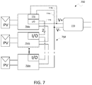
- FIG. 7 illustrates one embodiment of a photovoltaic system 700 where a voltage detection circuit is located within a module output circuit that is connected to a bus 768 that is connected to an inverter 770 .
- a voltage detection circuit is combined with a module output circuit and may be located in a common housing with the module output circuit, which may allow some sharing of resources thereby saving cost.
- a voltage detection circuit may be physically implemented as a circuit board in a module output circuit, or as a chip, programmable logic device (PLD) or other hardware.
- PLD programmable logic device
- a voltage detection may be implemented through firmware or software in a module output circuit, or may be implemented by a combination of hardware and software.
- Module output circuit 764 a includes a voltage detection circuit 776 that is connected to the output of bus 768 where it connects to input terminals of inverter 770 .
- Lead 774 a connects to a negative output (V ⁇ ) of bus 768 while lead 774 b connects to positive output (V+) of bus 768 and leads 774 a - b connect directly to voltage detection circuit 776 , which detects the voltage across the output of bus 768 (i.e. detects the voltage difference between the positive and negative outputs of bus 768 , which is the voltage provided to input terminals of inverter 770 ).
- Voltage detection circuit 776 may include a resistor network and ADC to provide an indicator of detected voltage as a digital output.
- This digital output may be used by a controller in module output circuit 764 a to control the output of module output circuit 764 a .
- the indicator of detected voltage is also sent from module output circuit 764 a , via its I/O circuit and communication channel 778 , to module output circuit 764 b , which uses the indicator of detected voltage to control its output.
- Module output circuit 764 b also passes the indicator of detected voltage to the next module output circuit, and so on from module output circuit to module output circuit of all photovoltaic modules connected to bus 768 .
- Module output circuit 764 n is shown as the last module output circuit attached to bus 768 so it does not provide the indicator of detected voltage to any subsequent module output circuits.
- FIG. 8 shows an embodiment in which each module output circuit 864 a - n connected to a bus 868 includes an analog-to-digital converter (ADC) 888 a - n .
- bus 868 provides an output to inverter 870 .
- Leads 874 a - b are attached to the output of bus 868 .
- Leads 874 a - b connect to a resistor network 866 that provides an analog output on communication channel 872 that is an indicator of detected voltage at the output of bus 868 .
- Resistor network 866 may be a simple circuit such as a voltage divider that is formed using resistors or other passive components.
- Communication channel 872 may be any suitable analog communication channel for conveying an analog signal including, for example, a wireless channel, or a wired channel formed by one or more conductive wires.
- Communication channel 872 connects to module output circuits 864 a - n to provide an indicator of detected bus voltage to each module output circuit connected to bus 868 .
- Each module output circuit 864 a - n includes an ADC 888 a - n which is connected to communication channel 872 .
- ADCs 888 a - n each receive an analog indicator of detected voltage through communication channel 872 and convert this analog indicator to a digital value. Controllers in module output circuits 864 a - n then use this digital indicator of detected voltage to control the output of respective module output circuits.
- module output circuit 864 a controls its output to bus 868 based on digital conversion of the indicator of detected voltage by ADC 888 a
- module output circuit 864 b controls its output to bus 868 based on digital conversion of the indicator of detected voltage by ADC 888 b
- an analog signal may be rapidly generated and broadcast to all module output circuits to allow rapid responses by module output circuits in this example.
- FIG. 9 illustrates operation of an embodiment which uses bus output voltage in each module output circuit to separately control module output voltages of modules connected to the bus.
- the scheme illustrated in FIG. 9 may be implemented using various hardware including hardware examples described in the present figures.
- the combined output voltage of the power modules connected in series by the bus (the bus output voltage) is detected 980 .
- the bus output voltage may be detected at or near where the bus output connects to input terminals of an inverter by an appropriate detection module.
- Leads may be attached to conductors at a suitable location and connected to suitable detection hardware which may include a resistor network.
- An indicator of the detected voltage is then generated 982 .
- the indicator of detected voltage may be, for example, an analog signal from a resistor network, or a digital indicator generated by an ADC, where a resistor network or ADC may be considered indicator generator modules.
- the indicator of detected voltage is then sent to each power module 984 through a communication channel.
- the indicator of detected voltage may be sent to controllers that are provided in module output circuits of each power module.
- Indicators of detected voltage may be sent through dedicated communication channels or may be sent through communication channels that are used for other data. Communication channels may be wired or wireless. Indicators of detected voltage may be sent in parallel to all power modules, or may be sent from power module to power module, or in any suitable manner.
- Indicators of detected voltage are then received 986 in module output circuits of each power module, which may be considered as indicator receiving modules.
- Individual power module output voltages are separately controlled 988 in response to the indicators of detected voltage received by the power modules. Outputs may be controlled by controllers in module output circuits.
- FIG. 10 illustrates an example of a module output circuit 1000 that includes a boost-buck circuit 1002 and a controller 1004 that controls boost-buck circuit 1002 .
- controller 1004 provides an output that controls a duty cycle of boost-buck circuit 1002 .
- a boost-buck circuit is an example of a switched-mode power circuit. The details of operation of a boost-buck circuit are well-known in the art.
- transistors in a boost-buck circuit act as switches that allow a capacitor to be alternately charged from an input that includes an inductor in a first phase, and discharged to an output in a second phase. The relative amounts of time spent charging in the first phase and discharging in the second phase may be controlled, for example, by the width of a pulse used to select between phases.
- boost-buck circuit 1002 may be controlled by a signal (gating signal) from a controller, such as a pulsed signal 1003 with pulse width modulation (PWM) to control duty cycle and thereby control the output of boost-buck circuit 1002 .
- Controller 1004 is connected to input and output terminals of boost-buck circuit 1002 so that controller 1004 is provided with data regarding conditions at the input and output terminals. Specifically, four different sensed parameters are provided to controller 1004 : on the input side, where module output circuit 1000 receives an electrical input from a photovoltaic panel (PV), a first input 1006 a indicates input current (current provided to module output circuit 1000 by the photovoltaic panel) and a second input 1006 b indicates input voltage (voltage across input terminals that is provided to module output circuit 1000 by the photovoltaic panel).
- PV photovoltaic panel
- a third input 1006 c indicates output current (current flowing from module output circuit 1000 to bus) and a fourth input 1006 d indicates output voltage (voltage across output terminals 1007 a , 1007 b that is provided to the bus).
- module output circuit 1000 In addition to the inputs indicating conditions at input and output terminals of module output circuit 1000 , module output circuit 1000 also receives an external input from outside module output circuit 1000 via communication channel 1008 .
- Communication channel 1008 is a wired communication channel with two conductors in this example. In other examples, a communication channel may optical (e.g. fiber optic), wireless, or other suitable channel.
- Communication channel 1008 provides additional input to controller 1004 , for controller 1004 to use when controlling duty cycle of boost-buck circuit 1002 . For example, communication channel 1008 may provide an indicator of bus output voltage that is detected at an output of the bus.
- controller 1004 is provided with external information including the total voltage provided by all modules attached to the bus (e.g. voltage at input terminals of an inverter).
- Communication channel 1008 is connected to an optocoupler 1010 .
- Optocoupler 1010 is a component that provides electrical isolation between communication channel 1008 and controller 1004 .
- an electrical input may be converted into light (e.g. by an LED or other light source) which is then converted back into an electrical output (e.g. by a photodiode). Converting an input into light and back into an electrical signal may isolate controller 1004 from potentially damaging voltages that could be present on communication channel 1008 .
- Optocoupler 1010 may be a digital optocoupler where communication channel 1008 is a digital communication channel (e.g. SPI channel) or may be a linear optocoupler where communication channel 1008 is a digital communication channel. Communication channel 1008 receives an input from the bus output where there may be high voltages (higher than present within any individual module). Thus, there is a risk that a high voltage could reach controller 1004 through communication channel 1008 . Optocoupler 1010 provides an isolating component between communication channel 1008 and controller 1004 to ensure that a high voltage on communication channel 1008 is not passed to controller 1004 .
- a digital communication channel e.g. SPI channel
- Communication channel 1008 receives an input from the bus output where there may be high voltages (higher than present within any individual module). Thus, there is a risk that a high voltage could reach controller 1004 through communication channel 1008 .
- Optocoupler 1010 provides an isolating component between communication channel 1008 and controller 1004 to ensure that a high voltage
- Controller 1004 provides an output to communication channel 1012 through an optocoupler 1014 .
- Communication channel 1012 extends to another module output circuit that is connected to the same bus (down bus in FIG. 10 ) and may convey information that the other module output circuit uses to regulate its output. For example, an indicator of detected bus output voltage that is received via communication channel 1008 may be sent out via communication channel 1012 .
- module output circuit 1000 passes on information to a subsequent module, which may in-turn pass the information to a subsequent module output circuit, and so on down the bus.
- communication channel 1008 may be directly connected to a bus output, or may be connected to another module output circuit on the same bus (up bus in FIG. 10 ), which in turn may connect to another module output circuit up to a module output circuit that is directly connected to a bus output.
- Each module output circuit connected to a bus may receive identical data that is relayed in a daisy-chain arrangement. Alternatively, there may be some differences in data received by different module output circuits.
- a module output circuit may add some data when sending on data that it received. For example, in addition to bus output voltage or other data received by module output circuit 1000 , duty cycle data, module output voltage and/or current, module input voltage and/or current, and/or other data may be sent to another module output circuit.
- a module output circuit that is downstream may receive information about module output circuits upstream, in addition to information about the overall bus output.
- Such communication is not limited to a single direction. Communication channels may be bi-directional so that data may be sent in either direction.
- bus output data may be sent in a particular direction
- other data may be send in the opposite direction along the same communication channels.
- controller 1004 may receive additional data over communication channel 1008 and or communication channel 1012 , which it may use to control the output of module output circuit 1000 .
- Module output circuits may establish communication via a handshake routine that establishes the number of modules attached to the bus and may establish characteristics of different modules so that each module output circuit may adjust its output based on overall system characteristics.
- FIG. 11 illustrates an example of a module output circuit 1100 that includes a buck-boost circuit 1102 and a controller 1104 that controls buck-boost circuit 1102 .
- controller 1104 provides an output that controls a duty cycle of buck-boost circuit 1102 .
- a buck-boost circuit is another example of a switched-mode power circuit that is similar to boost-buck circuit 1002 of FIG. 10 but with the inductor and capacitor locations changed. The details of operation of a buck-boost circuit are well-known in the art.
- transistors in a buck-boost circuit act as switches that allow a capacitor to be alternately charged from an input that includes an inductor in a first phase, and discharged to an output in a second phase.
- the relative amounts of time spent charging in the first phase and discharging in the second phase may be controlled, for example, by the width of a pulse used to select between phases.
- buck-boost circuit 1102 may be controlled by a signal (gating signal) from controller 1104 , such as a pulsed signal 1103 with pulse width modulation (PWM) to control duty cycle and thereby control the output of buck-boost circuit 1102 .
- PWM pulse width modulation
- Controller 1104 is connected to input and output terminals of buck-boost circuit 1102 so that controller 1104 is provided with data regarding conditions at the input and output terminals. Specifically, four different sensed parameters are provided to controller 1104 : on the input side, where module output circuit 1100 receives an electrical input from a photovoltaic panel (PV), a first input 1106 a indicates input current (current provided to module output circuit 1100 by the photovoltaic panel) and a second input 1106 b indicates input voltage (voltage across input terminals that is provided to module output circuit 1100 by the photovoltaic panel).
- PV photovoltaic panel
- a third input 1106 c indicates output current (current flowing from module output circuit 1100 to bus) and a fourth input 1106 d indicates output voltage (voltage across output terminals 1107 a , 1107 b that is provided to the bus).
- module output circuit 1100 In addition to the inputs indicating conditions at input and output terminals of module output circuit 1100 , module output circuit 1100 also receives an external input from outside module output circuit 1100 via communication channel 1008 .
- Communication channel 1108 is a wired communication channel with two conductors in this example. In other examples, a communication channel may optical (e.g. fiber optic), wireless, or other suitable channel. Communication channel 1108 provides additional input to controller 1104 , for controller 1104 to use when controlling duty cycle of buck-boost circuit 1102 . For example, communication channel 1108 may provide an indicator of bus output voltage that is detected at an output of the bus.
- controller 1104 is provided with external information including the total voltage provided by all modules attached to the bus (e.g. voltage at input terminals of an inverter).
- Communication channels 1108 is connected to an optocoupler 1109 as previously described with respect to FIG. 10 .
- Controller 1104 also provides an output to communication channel 1112 through an optocoupler 1114 .
- Communication channels 1108 and 1112 may operate similarly to communication channels 1008 and 1012 discussed above with respect to FIG. 10 .
- Module output circuits 1000 and 1100 provide two examples of module output circuits that include switched-mode power circuits that are controlled by a controller that receives an indicator of detected voltage from a bus output along with other parameters. Other module output circuits may use different switched-mode power circuits, or may use other power circuits (e.g. linear power circuits). A controller in a module output circuit may use the parameters provided to control a power circuit in various ways. Some examples are described below.
- FIG. 12 shows a schematic diagram of a module output circuit 1200 that includes a boost-buck circuit 1202 and a controller 1204 , which is shown in some detail.
- Controller 1204 includes a first analog-to-digital converter 1220 (A/D), which receives an indicator of input voltage 1206 a and an indicator of input current 1206 b from boost-buck circuit 1202 as previously described.
- Analog-to-digital converter 1220 generates digital values Ipv and Upv accordingly that represent input current and input voltage respectively from the photovoltaic panel (PV).
- Digital values Ipv and Upv are then sent to MPPT module 1222 .
- a Maximum Power Point Tracking (MPPT) scheme may be implemented by MPPT module 1222 according to any suitable system to keep the photovoltaic panel operating efficiently.
- MPPT Maximum Power Point Tracking
- MPPT module 1222 provides an output, Ref_Upv, that indicates a reference voltage for the photovoltaic panel that may be higher or lower than a detected voltage indicated by Upv in order to increase efficiency.
- Input side regulator 1224 receives Ref_Upv and generates Iref_PV in response.
- Iref_PV is sent to a multiplexer, MUX 1226 .
- MUX 1226 also receives other inputs and selects one of the inputs to generate an appropriate output, Ref_Imux to send to Current regulator 1228 .
- Current regulator 1228 then generates a reference, Ref_U to Pulse Width Modulation (PWM) generator 1230 , which provides a signal 1232 with a pulse width that controls the duty cycle of boost-buck circuit 1202 .
- PWM Pulse Width Modulation
- Derating circuit 1234 receives inputs Ipv and Upv (e.g. from analog-to-digital converter 1220 ) and a temperature indicator (“Temp”), which may be generated by a temperature measuring device (e.g. thermocouple) in module output circuit 1200 .
- Derating circuit 1234 generates output Iref_dr in response to the inputs it receives. In one example, derating circuit 1234 generates a default output when the temperature indicated as being below a threshold value and generates a different value when the temperature is indicated as being above a certain value. This may cause a reduction in power when temperature exceeds an acceptable value.
- boost-buck circuit 1202 On the output side of boost-buck circuit 1202 , output voltage and output current indicators are detected at output terminals 1207 a , 1207 b and indicators of output voltage and current, 1206 c and 1206 d respectively, are provided to an analog-to-digital converter 1236 in controller 1204 . Digital values Uout and Iout representing output voltage and current respectively are sent to output side regulator 1238 . Output side regulator 1238 also receives an input Ref_Uout from bus voltage management module 1240 . Bus voltage management module 1240 receives two inputs, Ref Ubal and Ubus. Input Ref_Ubal is received from cell balancing module 1242 , which generates Ref_Ubal in response to Iout and Uout (e.g. from analog-to-digital converter 1236 ) and Ubus from a programmable logic device, PLD 1244 .
- PLD 1244 programmable logic device
- PLD 1244 is connected to communications channels 1246 and 1248 through optocouplers 1245 a , 1245 b as previously described so that PLD 1244 may receive information regarding bus output voltage (e.g. an indicator of detected voltage at a bus output).
- PLD 1244 may be any suitable device including a field programmable gate array (FPGA), or complex PLD (CPLD).
- FPGA field programmable gate array
- CPLD complex PLD
- ASIC application specific integrated circuit
- PLD 1244 is responsible for external communication, including receiving data from elsewhere in the bus, such as an indicator of detected voltage, current, information from other module output circuits, etc.
- PLD 1244 generates output Ubus in response, which may be a digital value indicating bus output voltage (PLD 1244 may perform analog-to-digital conversion if communication channels 1246 and/or 1248 are analog).
- Output Ubus is sent to cell balancing module 1242 and also to bus voltage management module 1240 .
- bus voltage management module 1240 In response to Ubus, bus voltage management module 1240 generates Ref_Uout to change the output of the module output circuit in response to certain conditions. For example, when Ubus received from PLD 1244 indicates that bus voltage is high, then bus voltage management module 1240 may generate a value of Ref_Uout to reduce output voltage of module output circuit 1200 accordingly.
- bus voltage management module 1240 may generate Ref_Uout to increase output voltage of module output circuit 1200 accordingly.
- Bus voltage management module 1240 may react to transient conditions on the bus indicated by Ubus by selecting an appropriate Ref_Uout and sending it to output side regulator 1238 . If Ubus is in an acceptable range the bus voltage management module 1240 may generate Ref_Uout based on Ref_Ubal instead.
- Cell balancing module 1242 may also implement low voltage ride through (LVRT), zero voltage ride through (ZVRT), high voltage ride through (HVRT), and/or other routines to ensure the photovoltaic system operates safely and efficiently.
- bus voltage management module 1240 may change its output, Ref_Uout to react to the transient event.
- cell balancing module 1242 provides an output Rev_Ubal that may be indicated by a cell balancing or other routine and bus voltage management module 1240 may generate Ref_Uout based on Ref-Ubal under normal conditions (when there is no transient event).
- bus voltage management module 1240 may disregard Ref_Ubal and generate Ref_Uout to respond to the transient event. Thus, bus voltage management module 1240 acts to override regular output voltage management when a transient event occurs.
- Output side regulator 1238 provides an input Iref_ov to MUX 1226 according to Ref_Uout.
- MUX 1226 then generates output Ref_mux based on one of the inputs it receives. For example, during a transient event indicated by Ubus from PLD 1244 , Iref_ov may be set at a value that causes MUX 1226 to set Ref_mux to react to the transient event. At other times, MUX 1226 may select between the different inputs based on a prioritization scheme. In general, adjustment relating to MPPT, derating, and cell balancing may be performed over a longer time scale than adjustment made to respond to transient events.
- Such adjustment may be prioritized by comparing magnitudes of changes indicated, or some other comparison of inputs. For example, a small change indicated by derating circuit may receive a low priority, but if temperature continues to increase, an output voltage change indicated by Iref-dr will increase until, at some point, MUX 1226 responds by generating Ref_mux based on Iref_dr. It should be noted that MUX 1226 sends Ref_mux to input side regulator 1224 and output side regulator 1238 to provide feedback to these units so that they can provide input to MUX 1226 based on current conditions, i.e. provide input to adjust MUX 1226 output based on current output of MUX 1226 . MUX 1226 also receives feedback State_CR from current regulator 1228 , which in turn receives feedback State PW from PWM generator 1230 so that each unit is able to provide output to a subsequent unit based on the current condition of the subsequent unit.
- FIG. 13 is a schematic illustration of certain controller components in a module output circuit and shows how a controller may generate a control signal such as a PWM signal sent to a switched-mode power circuit, and particularly, how transient events may be handled.
- a voltage surge detection module 1302 receives an input Ubus that indicates the voltage at the output of the bus (this may be based on an indicator of detected voltage at the bus output) and compares it with a maximum value Ubus_max, which may be a preset parameter that is based on system requirements (e.g. regulatory requirements and/or specified limits for various components). When bus voltage exceeds a limit (e.g.
- Ubus>Ubus_max voltage surge detection module 1302 sends a signal, Enable 1 , to enable proportional integral controller, PI controller 1304 which then sends an output to switch 1306 that is based on a combination of present output voltage Uout of the module output circuit and the minimum output voltage indicated by Uout_min that is generated by combiner 1307 .
- PI controller 1304 may output a reference voltage to reduce output voltage from its present value, Uout, until it reaches a minimum set by Uout_min*.
- PI controller 1304 issues what may be considered a ramp-down output (“RampDown_Uout”) when it receives Enable 1 .
- Ref_Uout accordingly, e.g.
- Switch 1306 may be implemented as a multiplexer that selects one of its inputs as an output.
- the switch output may be provided to a PWM generator for example.
- a voltage dip detection module 1308 receives input Ubus and compares it with a minimum value Ubus_min, which may be a preset parameter that is based on system requirements (e.g. regulatory requirements and/or specified limits for various components). When bus voltage dips below a limit (e.g. Ubus ⁇ Ubus_min) then voltage dip detection module 1308 sends a signal, Enable 2 , to enable PI controller 1310 which then sends an output to switch 1306 that is based on a combination of present output voltage Uout of the module output circuit and the maximum output voltage indicated by Uout_max* generated by combiner 1311 .
- Ubus_min a preset parameter that is based on system requirements (e.g. regulatory requirements and/or specified limits for various components).
- PI controller 1310 may output a reference voltage to increase output voltage from its present value, Uout, until it reaches a maximum set by Uout_max*.
- PI controller 1310 issues what may be considered a ramp-up output (“RampUp_Uout”) when it receives Enable 2 .
- RamUp_Uout When switch 1306 receives this as an input it adjusts its output, Ref_Uout accordingly e.g. by passing RampUp_Uout as an output as Ref_Uout, thereby interrupting any other control signal in order to deal with a voltage dip.
- a transient event such as a voltage surge or voltage dip causes switch 1306 to change its output to either ramp output voltage up or down.
- RampDown_Uout or RampUp_Uout Whenever RampDown_Uout or RampUp_Uout is received, it overrides any other input to switch 1306 . Dealing with voltage surges may be prioritized over dealing with voltage dips by prioritizing RampDown_Uout over RampUp_Uout, though in practice, these inputs would not be expected to occur at the same time. Signals Enable 1 and Enable 2 are also provided to an adder 1312 that provides an input to switch 1306 . Thus, when either a voltage surge or a voltage dip is detected, a signal is passed to switch 1306 so that it can react accordingly and select an input from PI controller 1304 or PI controller 1310 accordingly.
- FIG. 14 is a flowchart that illustrates how a controller in a module output circuit may operate.
- An indicator of detected voltage at the output of the bus is received 1440 .
- a determination 1442 is made as to whether the bus voltage is in a surge. If the bus voltage is in a surge then an input reference is set to a preset parameter 1456 .
- a PI regulator is run 1446 using this input reference and a module output voltage reference is generated to ramp-down a module output voltage reference 1448 .
- a conditional switch unit selects this input 1449 (because it is a high priority input associated with a transient event).
- a new PWM signal is calculated for the new output voltage 1450 , based on the ramp-down module voltage reference received. This new PWM signal is then used to control module output duty cycle 1452 .
- the ratio of module power to total bus power is calculated 1458 .
- a droop algorithm is run 1460 using a small step (e.g. increment or decrement output voltage).
- a module output voltage reference is generated 1462 accordingly and is sent to a switch. If there is no higher priority input to the switch (e.g. if there is no ramp-up or ramp-down input triggered by a transient event) this input is used to calculate a PWM signal for the new output voltage 1450 , which is used to control module output circuit duty cycle 1452 .
- the droop algorithm controls duty cycle by making small modifications.
- an MPPT control algorithm may control duty cycle, or a combination of different algorithms can be used to collectively control duty cycle.
- PI proportional-integral
- the technology described herein can be implemented using hardware, software, or a combination of both hardware and software.
- the software used is stored on one or more of the processor readable storage devices described above to program one or more of the processors to perform the functions described herein.
- the processor readable storage devices can include computer readable media such as volatile and non-volatile media, removable and non-removable media.
- computer readable media may comprise computer readable storage media and communication media.
- Computer readable storage media is non-transitory and may be implemented in any method or technology for storage of information such as computer readable instructions, data structures, program modules or other data.
- Examples of computer readable storage media include RAM, ROM, EEPROM, flash memory or other memory technology, CD-ROM, digital versatile disks (DVD) or other optical disk storage, magnetic cassettes, magnetic tape, magnetic disk storage or other magnetic storage devices, or any other medium which can be used to store the desired information and which can be accessed by a computer.
- Communication media typically embodies computer readable instructions, data structures, program modules or other data in a modulated data signal such as a carrier wave or other transport mechanism and includes any information delivery media.
- modulated data signal means a signal that has one or more of its characteristics set or changed in such a manner as to encode information in the signal.
- communication media includes wired media such as a wired network or direct-wired connection, and wireless media such as RF and other wireless media. Combinations of any of the above are also included within the scope of computer readable media.
- some or all of the software can be replaced by dedicated hardware including custom integrated circuits, gate arrays, FPGAs, PLDs, and special purpose computers.
- software stored on a storage device
- the one or more processors can be in communication with one or more computer readable media/storage devices, peripherals and/or communication interfaces.
- some or all of the software can be replaced by dedicated hardware including custom integrated circuits, gate arrays, FPGAs, PLDs, and special purpose computers.
- a computer program may be stored or distributed on a suitable medium, such as an optical storage medium or a solid-state medium supplied together with, or as part of, other hardware, but may also be distributed in other forms, such as via the Internet or other wired or wireless telecommunication systems.
- a suitable medium such as an optical storage medium or a solid-state medium supplied together with, or as part of, other hardware, but may also be distributed in other forms, such as via the Internet or other wired or wireless telecommunication systems.
Landscapes
- Engineering & Computer Science (AREA)
- Power Engineering (AREA)
- Physics & Mathematics (AREA)
- Electromagnetism (AREA)
- General Physics & Mathematics (AREA)
- Radar, Positioning & Navigation (AREA)
- Automation & Control Theory (AREA)
- Inverter Devices (AREA)
Abstract
Description
Claims (22)
Priority Applications (1)
| Application Number | Priority Date | Filing Date | Title |
|---|---|---|---|
| US15/583,456 US10965126B2 (en) | 2017-05-01 | 2017-05-01 | Systems and methods for control of photovoltaic arrays |
Applications Claiming Priority (1)
| Application Number | Priority Date | Filing Date | Title |
|---|---|---|---|
| US15/583,456 US10965126B2 (en) | 2017-05-01 | 2017-05-01 | Systems and methods for control of photovoltaic arrays |
Publications (2)
| Publication Number | Publication Date |
|---|---|
| US20180316191A1 US20180316191A1 (en) | 2018-11-01 |
| US10965126B2 true US10965126B2 (en) | 2021-03-30 |
Family
ID=63916871
Family Applications (1)
| Application Number | Title | Priority Date | Filing Date |
|---|---|---|---|
| US15/583,456 Active 2037-05-31 US10965126B2 (en) | 2017-05-01 | 2017-05-01 | Systems and methods for control of photovoltaic arrays |
Country Status (1)
| Country | Link |
|---|---|
| US (1) | US10965126B2 (en) |
Cited By (1)
| Publication number | Priority date | Publication date | Assignee | Title |
|---|---|---|---|---|
| US11557780B2 (en) | 2020-04-20 | 2023-01-17 | Delta Electronics (Shanghai) Co., Ltd. | Fuel cell energy supply system and energy regulation method based on same |
Families Citing this family (3)
| Publication number | Priority date | Publication date | Assignee | Title |
|---|---|---|---|---|
| IT201800003122A1 (en) * | 2018-02-28 | 2019-08-28 | St Microelectronics Srl | POWER TRACKING CIRCUIT, CORRESPONDING SYSTEM AND PROCEDURE |
| US11165256B2 (en) * | 2019-10-09 | 2021-11-02 | Ming-Tsung Chen | Power supply system and power monitoring device |
| CN113131518B (en) * | 2021-04-19 | 2022-05-24 | 阳光电源股份有限公司 | MLPE photovoltaic system and MLPE equipment detection method thereof |
Citations (26)
| Publication number | Priority date | Publication date | Assignee | Title |
|---|---|---|---|---|
| US20080097655A1 (en) * | 2006-10-19 | 2008-04-24 | Tigo Energy, Inc. | Method and system to provide a distributed local energy production system with high-voltage DC bus |
| US7602808B2 (en) | 2001-03-29 | 2009-10-13 | International Business Machines Corporation | Method and system for network management providing access to application bandwidth usage calculations |
| US20110056533A1 (en) * | 2009-09-10 | 2011-03-10 | Kan-Sheng Kuan | Series solar system with current-matching function |
| US8004116B2 (en) | 2007-10-15 | 2011-08-23 | Ampt, Llc | Highly efficient solar power systems |
| US8013472B2 (en) | 2006-12-06 | 2011-09-06 | Solaredge, Ltd. | Method for distributed power harvesting using DC power sources |
| US8102074B2 (en) | 2009-07-30 | 2012-01-24 | Tigo Energy, Inc. | Systems and method for limiting maximum voltage in solar photovoltaic power generation systems |
| US20120206118A1 (en) * | 2011-02-10 | 2012-08-16 | Williams Bertrand J | Dynamic Frequency and Pulse-Width Modulation of Dual-Mode Switching Power Controllers in Photovoltaic Arrays |
| US20130026839A1 (en) * | 2011-07-28 | 2013-01-31 | Tigo Energy, Inc. | Systems and Methods to Combine Strings of Solar Panels |
| US20130194706A1 (en) * | 2012-01-30 | 2013-08-01 | Solaredge Technologies Ltd. | Photovoltaic Panel Circuitry |
| US8531055B2 (en) | 2006-12-06 | 2013-09-10 | Solaredge Ltd. | Safety mechanisms, wake up and shutdown methods in distributed power installations |
| US20130328397A1 (en) * | 2012-06-11 | 2013-12-12 | Samsung Sdi Co., Ltd. | Energy storage system |
| US20140152276A1 (en) * | 2012-11-30 | 2014-06-05 | Mitsubishi Electric Corporation | Dc/dc voltage converter and voltage conversion control method therefor |
| US8816535B2 (en) * | 2007-10-10 | 2014-08-26 | Solaredge Technologies, Ltd. | System and method for protection during inverter shutdown in distributed power installations |
| US20150137606A1 (en) * | 2012-05-25 | 2015-05-21 | Solaredge Technologies Ltd. | Circuit for interconnected direct current power sources |
| US20150188415A1 (en) * | 2013-12-30 | 2015-07-02 | King Abdulaziz City For Science And Technology | Photovoltaic systems with maximum power point tracking controller |
| US9088178B2 (en) | 2006-12-06 | 2015-07-21 | Solaredge Technologies Ltd | Distributed power harvesting systems using DC power sources |
| US20150303803A1 (en) * | 2012-01-06 | 2015-10-22 | Koninklijke Philips N.V. | Power converter with separate buck and boost conversion circuits |
| US20150372490A1 (en) * | 2013-02-14 | 2015-12-24 | Abb Technology Ltd | Method of Controlling a Solar Power Plant, A Power Conversion System, a DC/AC Inverter and a Solar Power Plant |
| US20160126847A1 (en) * | 2014-10-31 | 2016-05-05 | Majid Pahlevaninezhad | Current sensorless mppt for pv micro-inverters |
| US9366714B2 (en) | 2011-01-21 | 2016-06-14 | Ampt, Llc | Abnormality detection architecture and methods for photovoltaic systems |
| US9413268B2 (en) | 2012-05-10 | 2016-08-09 | Futurewei Technologies, Inc. | Multilevel inverter device and method |
| US9431825B2 (en) | 2011-07-28 | 2016-08-30 | Tigo Energy, Inc. | Systems and methods to reduce the number and cost of management units of distributed power generators |
| US9442504B2 (en) | 2009-04-17 | 2016-09-13 | Ampt, Llc | Methods and apparatus for adaptive operation of solar power systems |
| US9577425B1 (en) * | 2011-05-23 | 2017-02-21 | The Board Of Trustees Of The University Of Alabama | Systems and methods for controlling power switching converters for photovoltaic panels |
| US20170096327A1 (en) * | 2015-10-02 | 2017-04-06 | Franklin Fueling Systems, Inc. | Solar fueling station |
| US9866098B2 (en) * | 2011-01-12 | 2018-01-09 | Solaredge Technologies Ltd. | Serially connected inverters |
-
2017
- 2017-05-01 US US15/583,456 patent/US10965126B2/en active Active
Patent Citations (28)
| Publication number | Priority date | Publication date | Assignee | Title |
|---|---|---|---|---|
| US7602808B2 (en) | 2001-03-29 | 2009-10-13 | International Business Machines Corporation | Method and system for network management providing access to application bandwidth usage calculations |
| US20080097655A1 (en) * | 2006-10-19 | 2008-04-24 | Tigo Energy, Inc. | Method and system to provide a distributed local energy production system with high-voltage DC bus |
| US8013472B2 (en) | 2006-12-06 | 2011-09-06 | Solaredge, Ltd. | Method for distributed power harvesting using DC power sources |
| US8531055B2 (en) | 2006-12-06 | 2013-09-10 | Solaredge Ltd. | Safety mechanisms, wake up and shutdown methods in distributed power installations |
| US9088178B2 (en) | 2006-12-06 | 2015-07-21 | Solaredge Technologies Ltd | Distributed power harvesting systems using DC power sources |
| US8816535B2 (en) * | 2007-10-10 | 2014-08-26 | Solaredge Technologies, Ltd. | System and method for protection during inverter shutdown in distributed power installations |
| US8004116B2 (en) | 2007-10-15 | 2011-08-23 | Ampt, Llc | Highly efficient solar power systems |
| US9442504B2 (en) | 2009-04-17 | 2016-09-13 | Ampt, Llc | Methods and apparatus for adaptive operation of solar power systems |
| US8102074B2 (en) | 2009-07-30 | 2012-01-24 | Tigo Energy, Inc. | Systems and method for limiting maximum voltage in solar photovoltaic power generation systems |
| US8274172B2 (en) | 2009-07-30 | 2012-09-25 | Tigo Energy, Inc. | Systems and method for limiting maximum voltage in solar photovoltaic power generation systems |
| US20110056533A1 (en) * | 2009-09-10 | 2011-03-10 | Kan-Sheng Kuan | Series solar system with current-matching function |
| US9866098B2 (en) * | 2011-01-12 | 2018-01-09 | Solaredge Technologies Ltd. | Serially connected inverters |
| US9366714B2 (en) | 2011-01-21 | 2016-06-14 | Ampt, Llc | Abnormality detection architecture and methods for photovoltaic systems |
| US20120206118A1 (en) * | 2011-02-10 | 2012-08-16 | Williams Bertrand J | Dynamic Frequency and Pulse-Width Modulation of Dual-Mode Switching Power Controllers in Photovoltaic Arrays |
| US9577425B1 (en) * | 2011-05-23 | 2017-02-21 | The Board Of Trustees Of The University Of Alabama | Systems and methods for controlling power switching converters for photovoltaic panels |
| US20130026839A1 (en) * | 2011-07-28 | 2013-01-31 | Tigo Energy, Inc. | Systems and Methods to Combine Strings of Solar Panels |
| US9431825B2 (en) | 2011-07-28 | 2016-08-30 | Tigo Energy, Inc. | Systems and methods to reduce the number and cost of management units of distributed power generators |
| US20150303803A1 (en) * | 2012-01-06 | 2015-10-22 | Koninklijke Philips N.V. | Power converter with separate buck and boost conversion circuits |
| US20150171789A1 (en) * | 2012-01-30 | 2015-06-18 | Solaredge Technologies Ltd. | Photovoltaic Panel Circuitry |
| US20130194706A1 (en) * | 2012-01-30 | 2013-08-01 | Solaredge Technologies Ltd. | Photovoltaic Panel Circuitry |
| US9413268B2 (en) | 2012-05-10 | 2016-08-09 | Futurewei Technologies, Inc. | Multilevel inverter device and method |
| US20150137606A1 (en) * | 2012-05-25 | 2015-05-21 | Solaredge Technologies Ltd. | Circuit for interconnected direct current power sources |
| US20130328397A1 (en) * | 2012-06-11 | 2013-12-12 | Samsung Sdi Co., Ltd. | Energy storage system |
| US20140152276A1 (en) * | 2012-11-30 | 2014-06-05 | Mitsubishi Electric Corporation | Dc/dc voltage converter and voltage conversion control method therefor |
| US20150372490A1 (en) * | 2013-02-14 | 2015-12-24 | Abb Technology Ltd | Method of Controlling a Solar Power Plant, A Power Conversion System, a DC/AC Inverter and a Solar Power Plant |
| US20150188415A1 (en) * | 2013-12-30 | 2015-07-02 | King Abdulaziz City For Science And Technology | Photovoltaic systems with maximum power point tracking controller |
| US20160126847A1 (en) * | 2014-10-31 | 2016-05-05 | Majid Pahlevaninezhad | Current sensorless mppt for pv micro-inverters |
| US20170096327A1 (en) * | 2015-10-02 | 2017-04-06 | Franklin Fueling Systems, Inc. | Solar fueling station |
Non-Patent Citations (4)
| Title |
|---|
| Adhikari, et al., P-Q and P-V Control of Photovoltaic Generators in Distribution Systems, IEEE Transactions on Smart Grid, Nov. 2015, pp. 2929-2941, vol. 6, No. 6. |
| Ding et al., Adaptive DC-Link Voltage Control of Two-Stage Photovoltaic Inverter During Low Voltage Ride-Through Operation, IEEE Transactions on Power Electronics, Jun. 2016, pp. 4182-4194, vol. 31, No. 6. |
| Jain et al., A Three-Phase Grid Tied SPV System with Adaptive DC Link Voltage for CPI Voltage Variations, IEEE Transactions of Sustainable Energy, Jan. 2016, pp. 337-344, vol. 7, No. 1. |
| Liu et al., Droop Control with Improved Disturbance Adaption for a PV System with Two Power Conversion Stages, IEEE Transactions on Industrial Electronics, Oct. 2016, pp. 6073-6085, vol. 63, No. 10. |
Cited By (1)
| Publication number | Priority date | Publication date | Assignee | Title |
|---|---|---|---|---|
| US11557780B2 (en) | 2020-04-20 | 2023-01-17 | Delta Electronics (Shanghai) Co., Ltd. | Fuel cell energy supply system and energy regulation method based on same |
Also Published As
| Publication number | Publication date |
|---|---|
| US20180316191A1 (en) | 2018-11-01 |
Similar Documents
| Publication | Publication Date | Title |
|---|---|---|
| US10770988B2 (en) | Non-linear droop control | |
| US10965126B2 (en) | Systems and methods for control of photovoltaic arrays | |
| US8102074B2 (en) | Systems and method for limiting maximum voltage in solar photovoltaic power generation systems | |
| AU2016202027B2 (en) | Automatic voltage regulation for photovoltaic systems | |
| JP6025238B2 (en) | Method and system for operating a two-stage power converter | |
| US11437823B2 (en) | Power systems with inverter input voltage control | |
| KR20160081067A (en) | Low Voltage DC Distribution System and Distribution Method thereof | |
| US9285816B2 (en) | Harvesting power from DC (direct current) sources | |
| CN113452074B (en) | Photovoltaic system and control method | |
| AU2019300646A1 (en) | Power conversion system, method for controlling converter circuit, and program | |
| US10014690B2 (en) | Double-stage inverter apparatus for energy conversion systems and control method thereof | |
| US11329488B2 (en) | Power conversion system, method for controlling converter circuit, and program | |
| US10381842B2 (en) | Power supply system | |
| KR20130102390A (en) | Active power limitation method | |
| US20230291208A1 (en) | Photovoltaic power generation system, photovoltaic inverter, and iv curve scanning method | |
| US10523014B2 (en) | Control of a multiple input solar power inverter | |
| US20180183240A1 (en) | Power conversion apparatus, power conversion method, and power conversion system | |
| US11626834B2 (en) | Power backfeed control method, converter, and photovoltaic power generation system | |
| CN115242059A (en) | Multi-power-supply parallel current output device and method and electronic equipment | |
| US11394235B2 (en) | Power conversion system and method | |
| US20120193989A1 (en) | Operating direct current (dc) power sources in an array for enhanced efficiency |
Legal Events
| Date | Code | Title | Description |
|---|---|---|---|
| AS | Assignment |
Owner name: FUTUREWEI TECHNOLOGIES, INC., TEXAS Free format text: ASSIGNMENT OF ASSIGNORS INTEREST;ASSIGNORS:ZHU, HUIBIN;DAI, HEPING;MAO, XIAOLIN;REEL/FRAME:042879/0717 Effective date: 20170508 |
|
| STPP | Information on status: patent application and granting procedure in general |
Free format text: NON FINAL ACTION MAILED |
|
| STPP | Information on status: patent application and granting procedure in general |
Free format text: FINAL REJECTION MAILED |
|
| STPP | Information on status: patent application and granting procedure in general |
Free format text: DOCKETED NEW CASE - READY FOR EXAMINATION |
|
| STPP | Information on status: patent application and granting procedure in general |
Free format text: NON FINAL ACTION MAILED |
|
| STPP | Information on status: patent application and granting procedure in general |
Free format text: RESPONSE TO NON-FINAL OFFICE ACTION ENTERED AND FORWARDED TO EXAMINER |
|
| STPP | Information on status: patent application and granting procedure in general |
Free format text: NOTICE OF ALLOWANCE MAILED -- APPLICATION RECEIVED IN OFFICE OF PUBLICATIONS |
|
| STPP | Information on status: patent application and granting procedure in general |
Free format text: PUBLICATIONS -- ISSUE FEE PAYMENT VERIFIED |
|
| STCF | Information on status: patent grant |
Free format text: PATENTED CASE |
|
| AS | Assignment |
Owner name: HUAWEI DIGITAL POWER TECHNOLOGIES CO., LTD., CHINA Free format text: ASSIGNMENT OF ASSIGNORS INTEREST;ASSIGNOR:FUTUREWEI TECHNOLOGIES, INC.;REEL/FRAME:058601/0723 Effective date: 20211230 |