US10637370B2 - Apparatus for controlling DC-AC converter to reduce distortions in output current - Google Patents
Apparatus for controlling DC-AC converter to reduce distortions in output current Download PDFInfo
- Publication number
- US10637370B2 US10637370B2 US16/253,699 US201916253699A US10637370B2 US 10637370 B2 US10637370 B2 US 10637370B2 US 201916253699 A US201916253699 A US 201916253699A US 10637370 B2 US10637370 B2 US 10637370B2
- Authority
- US
- United States
- Prior art keywords
- current
- correction
- converter
- reactor
- switch
- Prior art date
- Legal status (The legal status is an assumption and is not a legal conclusion. Google has not performed a legal analysis and makes no representation as to the accuracy of the status listed.)
- Active
Links
Images


Classifications
-
- H—ELECTRICITY
- H02—GENERATION; CONVERSION OR DISTRIBUTION OF ELECTRIC POWER
- H02M—APPARATUS FOR CONVERSION BETWEEN AC AND AC, BETWEEN AC AND DC, OR BETWEEN DC AND DC, AND FOR USE WITH MAINS OR SIMILAR POWER SUPPLY SYSTEMS; CONVERSION OF DC OR AC INPUT POWER INTO SURGE OUTPUT POWER; CONTROL OR REGULATION THEREOF
- H02M7/00—Conversion of ac power input into dc power output; Conversion of dc power input into ac power output
- H02M7/42—Conversion of dc power input into ac power output without possibility of reversal
- H02M7/44—Conversion of dc power input into ac power output without possibility of reversal by static converters
- H02M7/48—Conversion of dc power input into ac power output without possibility of reversal by static converters using discharge tubes with control electrode or semiconductor devices with control electrode
- H02M7/53—Conversion of dc power input into ac power output without possibility of reversal by static converters using discharge tubes with control electrode or semiconductor devices with control electrode using devices of a triode or transistor type requiring continuous application of a control signal
- H02M7/537—Conversion of dc power input into ac power output without possibility of reversal by static converters using discharge tubes with control electrode or semiconductor devices with control electrode using devices of a triode or transistor type requiring continuous application of a control signal using semiconductor devices only, e.g. single switched pulse inverters
- H02M7/5387—Conversion of dc power input into ac power output without possibility of reversal by static converters using discharge tubes with control electrode or semiconductor devices with control electrode using devices of a triode or transistor type requiring continuous application of a control signal using semiconductor devices only, e.g. single switched pulse inverters in a bridge configuration
-
- H—ELECTRICITY
- H02—GENERATION; CONVERSION OR DISTRIBUTION OF ELECTRIC POWER
- H02M—APPARATUS FOR CONVERSION BETWEEN AC AND AC, BETWEEN AC AND DC, OR BETWEEN DC AND DC, AND FOR USE WITH MAINS OR SIMILAR POWER SUPPLY SYSTEMS; CONVERSION OF DC OR AC INPUT POWER INTO SURGE OUTPUT POWER; CONTROL OR REGULATION THEREOF
- H02M1/00—Details of apparatus for conversion
- H02M1/12—Arrangements for reducing harmonics from ac input or output
-
- H—ELECTRICITY
- H02—GENERATION; CONVERSION OR DISTRIBUTION OF ELECTRIC POWER
- H02M—APPARATUS FOR CONVERSION BETWEEN AC AND AC, BETWEEN AC AND DC, OR BETWEEN DC AND DC, AND FOR USE WITH MAINS OR SIMILAR POWER SUPPLY SYSTEMS; CONVERSION OF DC OR AC INPUT POWER INTO SURGE OUTPUT POWER; CONTROL OR REGULATION THEREOF
- H02M1/00—Details of apparatus for conversion
- H02M1/42—Circuits or arrangements for compensating for or adjusting power factor in converters or inverters
- H02M1/4208—Arrangements for improving power factor of AC input
- H02M1/4225—Arrangements for improving power factor of AC input using a non-isolated boost converter
-
- H—ELECTRICITY
- H02—GENERATION; CONVERSION OR DISTRIBUTION OF ELECTRIC POWER
- H02M—APPARATUS FOR CONVERSION BETWEEN AC AND AC, BETWEEN AC AND DC, OR BETWEEN DC AND DC, AND FOR USE WITH MAINS OR SIMILAR POWER SUPPLY SYSTEMS; CONVERSION OF DC OR AC INPUT POWER INTO SURGE OUTPUT POWER; CONTROL OR REGULATION THEREOF
- H02M7/00—Conversion of ac power input into dc power output; Conversion of dc power input into ac power output
- H02M7/42—Conversion of dc power input into ac power output without possibility of reversal
- H02M7/44—Conversion of dc power input into ac power output without possibility of reversal by static converters
- H02M7/48—Conversion of dc power input into ac power output without possibility of reversal by static converters using discharge tubes with control electrode or semiconductor devices with control electrode
- H02M7/53—Conversion of dc power input into ac power output without possibility of reversal by static converters using discharge tubes with control electrode or semiconductor devices with control electrode using devices of a triode or transistor type requiring continuous application of a control signal
- H02M7/537—Conversion of dc power input into ac power output without possibility of reversal by static converters using discharge tubes with control electrode or semiconductor devices with control electrode using devices of a triode or transistor type requiring continuous application of a control signal using semiconductor devices only, e.g. single switched pulse inverters
- H02M7/5387—Conversion of dc power input into ac power output without possibility of reversal by static converters using discharge tubes with control electrode or semiconductor devices with control electrode using devices of a triode or transistor type requiring continuous application of a control signal using semiconductor devices only, e.g. single switched pulse inverters in a bridge configuration
- H02M7/53871—Conversion of dc power input into ac power output without possibility of reversal by static converters using discharge tubes with control electrode or semiconductor devices with control electrode using devices of a triode or transistor type requiring continuous application of a control signal using semiconductor devices only, e.g. single switched pulse inverters in a bridge configuration with automatic control of output voltage or current
-
- H—ELECTRICITY
- H02—GENERATION; CONVERSION OR DISTRIBUTION OF ELECTRIC POWER
- H02M—APPARATUS FOR CONVERSION BETWEEN AC AND AC, BETWEEN AC AND DC, OR BETWEEN DC AND DC, AND FOR USE WITH MAINS OR SIMILAR POWER SUPPLY SYSTEMS; CONVERSION OF DC OR AC INPUT POWER INTO SURGE OUTPUT POWER; CONTROL OR REGULATION THEREOF
- H02M1/00—Details of apparatus for conversion
- H02M1/0003—Details of control, feedback or regulation circuits
- H02M1/0025—Arrangements for modifying reference values, feedback values or error values in the control loop of a converter
-
- H02M2001/0025—
-
- Y—GENERAL TAGGING OF NEW TECHNOLOGICAL DEVELOPMENTS; GENERAL TAGGING OF CROSS-SECTIONAL TECHNOLOGIES SPANNING OVER SEVERAL SECTIONS OF THE IPC; TECHNICAL SUBJECTS COVERED BY FORMER USPC CROSS-REFERENCE ART COLLECTIONS [XRACs] AND DIGESTS
- Y02—TECHNOLOGIES OR APPLICATIONS FOR MITIGATION OR ADAPTATION AGAINST CLIMATE CHANGE
- Y02B—CLIMATE CHANGE MITIGATION TECHNOLOGIES RELATED TO BUILDINGS, e.g. HOUSING, HOUSE APPLIANCES OR RELATED END-USER APPLICATIONS
- Y02B70/00—Technologies for an efficient end-user side electric power management and consumption
- Y02B70/10—Technologies improving the efficiency by using switched-mode power supplies [SMPS], i.e. efficient power electronics conversion e.g. power factor correction or reduction of losses in power supplies or efficient standby modes
Definitions
- the present disclosure relates to an apparatus for controlling a DC-AC converter that converts direct-current (DC) power into alternating-current (AC) power.
- An apparatus for controlling an AC-DC converter operative to convert alternating-current (AC) power supplied from an AC power source into direct-current (DC) power is known that is configured to operate drive switches with well-known peak current mode control to thereby control a reactor current through a reactor to a command value.
- An apparatus for controlling the AC-DC converter disclosed in JP-A-2015-198460, is configured to superimpose current correction values on the command values for the reactor currents to reduce distortions in input currents near zero crossings where a voltage supplied from the AC power source is zero. As described in JP-A-2015-198460, the current correction values are set such that the command values near zero crossings are more increased than during other periods.
- a DC-AC converter is operative to convert DC power supplied via an input terminal into AC power and supply the alternating-current (AC) power after conversion to the AC power source. Also in such a converter, reducing distortions in output currents can improve a power factor of AC power to be supplied to the AC power source.
- the DC-AC converter is different in circuit topology from the AC-DC converter. Thus, the technique for reducing distortions in input currents of the AC-DC converter as disclosed in JP-A-2015-198460 is not directly applicable to the DC-AC converter.
- One aspect of the disclosure provides an apparatus for controlling a DC-AC converter including a reactor and a plurality of drive switches and configured to convert DC power supplied via input terminals into AC power and supply the AC power to an AC power source connected to output terminals.
- the DC-AC converter is provided with a current detector configured to detect a reactor current through the reactor.
- a current corrector is configured to set a current correction value including a harmonic component for a frequency component of a supply voltage of the AC power source that has minima at zero crossings where the supply voltage is zero and superimpose the current correction value on a sinusoidal commanded current generated based on the supply voltage of the AC power source, thereby generating a commanded current after correction.
- a current controller is configured to operate the drive switches using peak current mode control to control the reactor current to the commanded current after correction.
- the on-period of the drive switches is set to control the reactor current to the commanded current.
- the commanded current is set to have a sinusoidal wave such that the output current of the DC-AC converter takes a value responsive to a phase of the supply voltage of the AC power source, a discrepancy between the commanded reactor current and the average of reactor current at zero crossings where the supply voltage of the AC power source is zero are smaller than during the other periods.
- the commanded current after correction in the peak current mode control may cause the on-period of the drive switches to increase above or decrease below its proper value, which may lead to increased current distortions near zero crossings.
- the current controller is configured to set the current correction value including the harmonic component for the frequency component of the supply voltage that has minima at zero crossings.
- the current controller is further configured to correct the sinusoidal commanded reactor current by adding the current correction value thereto.
- FIG. 1 is a circuit diagram of a power converter in accordance with a first embodiment of the present disclosure
- FIG. 2 is a functional block diagram of a controller
- FIG. 3 is a timing diagram for a DC-AC converter
- FIG. 4 is a functional block diagram of a current corrector
- FIG. 5 is an example of a current correction value
- FIG. 6 is an example of a change in a commanded current after correction ILa*
- FIG. 7 is an illustration of a discrepancy
- FIG. 8 is a flowchart of processing performed by the DC-AC converter
- FIG. 9 is an example of a change in an output current acquired by correcting commanded current before correction using current correction values
- FIG. 10 is a comparative example of a change in an output current where commanded current before correction is not corrected
- FIG. 11 is a functional block diagram of a current corrector in accordance with a second embodiment
- FIG. 12 is a flowchart of processing performed by the DC-AC converter according to the second embodiment.
- FIG. 13 is an example of harmonic maps stored in a harmonic generator according to a third embodiment
- FIG. 14 is a circuit diagram of a power converter according to a fourth embodiment.
- FIG. 15 is a functional block diagram of a controller according to the fourth embodiment.
- FIG. 16 is a timing diagram for a DC-AC converter according to the fourth embodiment.
- FIG. 17 is a circuit diagram of a power converter according to a modification to the fourth embodiment.
- FIG. 18 is a functional block diagram of a controller according to the modification to the fourth embodiment.
- FIG. 19 is a circuit diagram of a power converter in accordance with a fifth embodiment.
- FIG. 20 is a functional block diagram of a controller according to a fifth embodiment.
- FIG. 21 is a timing diagram for a DC-AC converter according to the fifth embodiment.
- the power converter is electrically connected to an AC power source and converts direct-current (DC) power supplied via input terminals into alternating-current (AC) power to supply the AC power to the AC power source.
- DC direct-current
- AC alternating-current
- FIG. 1 illustrates a circuit diagram of the power converter 100 in accordance with the present embodiment.
- the power converter 100 includes a DC-AC converter 10 and a controller 30 .
- a DC power source (not shown) is connected between a first input terminal IN 1 and a second input terminal IN 2 of the DC-AC converter 10 .
- An AC power source 200 is connected between a first output terminal OUT 1 and a second output terminal OUT 2 of the DC-AC converter 10 .
- the AC power source 200 may be a commercially available power source.
- the DC power source may be a battery.
- the DC-AC converter 10 includes a capacitor 16 , a half-bridge circuit 15 , a reactor 13 , a full-bridge circuit 12 , and first to sixth wirings LP 1 -LP 6 .
- a wiring of the DC-AC converter 10 connected to the first input terminal IN 1 is referred to as a first wiring LP 1 .
- Another wiring of the DC-AC converter 10 connected to a second input terminal IN 2 is referred to as a second wiring LP 2 .
- a high voltage side wiring included in the DC-AC converter 10 connecting the half-bridge circuit 15 and the full-bridge circuit 12 is referred to as a third wiring LP 3 .
- a low voltage side wiring included in the DC-AC converter 10 connecting the half-bridge circuit 15 and the full-bridge circuit 12 is referred to as a fourth wiring LP 4 .
- a wiring of the DC-AC converter 10 connected to the first output terminal OUT 1 is referred to as a fifth wiring LP 5 .
- a wiring of the DC-AC converter 10 connected to the second output terminal OUT 2 is referred to as a sixth wiring LP 6 .
- a first end of the capacitor 16 is connected to the first wiring LP 1 and a second end of the capacitor 16 is connected to the second wiring LP 2 .
- the half-bridge circuit 15 includes a first switch Q 1 and a second switch Q 2 .
- the first and second switches Q 1 , Q 2 are voltage-driven switches, which are N-channel MOSFETs in the present embodiment.
- a source of the first switch Q 1 and a drain of the second switch Q 2 are connected to each other.
- a drain of the first switch Q 1 is connected to the first wiring LP 1 .
- a source of the second switch Q 2 is connected to the second wiring LP 2 .
- Each of the first and second switches Q 1 , Q 2 has a parasitic diode connected in anti-parallel therewith.
- the first switch Q 1 corresponds to a drive switch.
- a first connection point K 1 between the first and second switches Q 1 , Q 2 is connected to a first end of the third wiring LP 3 .
- the reactor 13 is provided along the third wiring LP 3 .
- the source of the second switch Q 2 of the half-bridge circuit 15 is connected to a first end of the fourth wiring LP 4 .
- Second ends of the third and fourth wirings LP 3 , LP 4 are connected to the full-bridge circuit 12 .
- the full-bridge circuit 12 includes third to sixth switches Q 3 -Q 6 .
- the third to sixth switches Q 3 to Q 6 are voltage-driven switches, which are N-channel MOSFETs in the present embodiment.
- a source of the third switch Q 3 and a drain of the fourth switch Q 4 are connected to each other.
- a source of the fifth switch Q 5 and a drain of the sixth switch Q 6 are connected to each other.
- Drains of the third and fifth switches Q 3 , Q 5 are connected to the third wirings LP 3 .
- Sources of the fourth and sixth switches Q 4 , Q 6 are connected to the fourth wiring LP 4 .
- a second connection point K 2 between the third switch Q 3 and the fourth switch Q 4 is connected to a first end of the sixth wiring LP 6 .
- a second end of the sixth wiring LP 6 is connected to the second output terminal OUT 2 .
- a third connection point K 3 between the fifth switch Q 5 and the sixth switch Q 6 is connected to a first end of the fifth wiring LP 5 .
- a second end of the fifth wiring LP 5 is connected to the first output terminal OUT 1 .
- the power converter 100 includes a first voltage sensor 31 , a current sensor 32 , and a second voltage sensor 33 .
- the first voltage sensor 31 corresponds to a voltage detector.
- the first voltage sensor 31 is connected between the first and second wirings LP 1 , LP 2 on the opposite side of the capacitor 16 from the half-bridge circuit 15 to detect a DC voltage input via the first and second input terminals IN 1 , IN 2 as an input voltage Vdc.
- the current sensor 32 is provided along the fourth wiring LP 4 to detect a reactor current ILr through the reactor 13 .
- the second voltage sensor 33 between the first and second output terminals OUT 1 , OUT 2 and the full-bridge circuit 12 , is connected between the fifth and sixth wirings LP 5 , LP 6 to detect a voltage of the AC power source 200 as a supply voltage Vac.
- the controller 30 is configured to control the open/closed state of each of the first to sixth switches Q 1 -Q 6 of the DC-AC converter 10 .
- Various functions of the controller 10 may be implemented by software stored in a tangible memory device and a computer that executes it, hardware, or a combination thereof.
- FIG. 2 is a functional block diagram of the controller 30 .
- the controller 30 is configured to, with well-known peak current mode control, control each of the first and second switches Q 1 , Q 2 from an open/closed state to a closed/open state.
- the controller 30 includes a waveform generator 34 , a multiplier 35 , an absolute value calculator 36 , an adder 37 , a current corrector 40 , a current controller 50 , and a polarity switcher 55 .
- the waveform generator 34 is configured to generate a reference waveform
- the waveform generator 34 sets an angular speed of a sinusoidal wave signal with an amplitude of 1 to the calculated angular speed, thereby calculating the reference waveform
- the multiplier 35 is configure to multiply an amplitude command value Ia* of the reactor current ILr and the reference waveform
- the amplitude command value Ia* is a command value for the amplitude of the reactor current ILr, which may be determined based on a voltage command value.
- the absolute value calculator 36 is configured to set an absolute value of an output value from the multiplier 35 as a commanded current before correction IL*. In the present embodiment, the commanded current before correction IL* corresponds to the commanded reactor current.
- the current corrector 40 is configured to set a current correction value Ic for correcting the commanded current before correction IL*.
- the current correction value Ic is a correction value for reducing distortions in the output current Iac.
- the current corrector 40 is configured to set a current correction value Ic based on the supply voltage Vac and the commanded current before correction IL*.
- the adder 37 is configured to add the current correction value Ic to an absolute value of the commanded current before correction IL* to set the resultant value as a commanded current after correction ILa*.
- the current controller 50 is configured to, based on the reactor current ILr detected by the current sensor 32 and the commanded current after correction ILa*, generate a first gate signal GS 1 for operating the first switch Q 1 and a second gate signal GS 2 for operating the second switch Q 2 .
- the current controller 50 generates the first and second gate signals GS 1 , GS 2 using well-known peak current mode control.
- the current controller 50 includes a digital-to-analog (DA) converter 351 , a comparator 352 , an adder 353 , and an RS flip-flop 357 .
- the commanded current after correction ILa* is input to the DA converter 351 .
- the DA converter 351 is configured to digital-to-analog convert the received commanded current after correction ILa*.
- the resultant analog commanded current after correction ILa* is input to an inverting input terminal of the comparator 352 .
- the adder 353 is configured to add the reactor current ILr and the slope compensation signal Slope to output a reactor current after compensation ILcr that is a sum of the reactor current ILr and the slope compensation signal Slope.
- the output of the adder 353 is input to a non-inverting input terminal of the comparator 352 .
- the slope compensation signal Slope suppresses oscillation caused by variations in current through the reactor 13 .
- the comparator 352 is configured to compare the commanded current after correction ILa* and the reactor current after compensation ILcr and input a signal in the LOW state to an R terminal of the RS flip-flop 357 during a period in time where the reactor current after compensation ILcr is lower than the commanded current after correction ILa*.
- the comparator 352 is further configured to input a signal in the HIGH state to the R terminal of the RS flip-flop 357 during a period in time where the reactor current after compensation ILcr is higher than the commanded current after correction ILa*.
- a clock signal is input to the S terminal of the RS flip-flop 357 .
- the Q terminal of the RS flip-flop 357 is connected to the gate of the first switch Q 1 .
- the first gate signal GS 1 is output from the Q terminal to the gate of the first switch Q 1 .
- the output terminal of the RS flip-flop 357 is connected through an inverter 358 to the gate of the second switch Q 2 .
- the second gate signal GS 2 is output from the Q terminal through the inverter 358 to the gate of the second switch Q 2 .
- the second gate signal GS 2 is the inverse of the value of the first gate signal GS 1 .
- the polarity switcher 55 is configured to invert the output signal in response to the polarity of the supply voltage Vac.
- the polarity switcher 55 is configured to, if determining that the polarity of the supply voltage Vac is positive, place the output signal from the output terminal in a HIGH state.
- the polarity switcher 55 is configured to, if determining that the polarity of the supply voltage Vac is negative, place the output signal from the output terminal in a LOW state.
- the output terminal of the polarity switcher 55 is connected to the gate of each of the third and sixth switches Q 3 , Q 6 .
- a signal output from the output terminal of the polarity switcher 55 to the gate of third switch Q 3 is a third gate signal GS 3 .
- a signal output from the output terminal of the polarity switcher 55 to the gate of sixth switch Q 6 is a sixth gate signal GS 6 .
- the output terminal of the polarity switcher 55 is connected to the gate of each of the fourth and fifth switches Q 4 , Q 5 through the inverter 359 .
- a signal output from the output terminal of the polarity switcher 55 through the inverter 359 to the gate of fourth switch Q 4 is a fourth gate signal GS 4 .
- a signal output from the output terminal of the polarity switcher 55 through the inverter 359 to the gate of fifth switch Q 5 is a fifth gate signal GS 5 .
- Each of the fourth and fifth gate signals GS 4 , GS 5 is the inverse of a respective one of the third and sixth gate signals GS 3 , GS 6 .
- FIG. 3 is a timing diagram for the DC-AC converter 10 of the present embodiment.
- FIG. 3( a ) illustrates an example of a change in each of the input voltage Vdc and the supply voltage Vac.
- FIG. 3( b ) illustrates an example of a change in each of the fourth and fifth gate signals GS 4 , GS 5 .
- FIG. 3( c ) illustrates an example of a change in each of the third and sixth gate signals GS 3 , GS 6 .
- FIG. 3( d ) illustrates an example of a change in the first gate signal GS 1 .
- FIG. 3( e ) illustrates an example of a change in the second gate signal.
- FIG. 3( f ) illustrates an example of a change in the commanded current after correction ILa*.
- FIG. 3( g ) illustrates an example of a change in the reactor current ILr.
- the fourth and fifth gate signals GS 4 , GS 5 in the HIGH state place the fourth and fifth switches Q 4 , Q 5 in the closed state, respectively.
- the third and sixth gate signals GS 3 , GS 6 in the LOW state place the third and sixth switches Q 3 , Q 6 in the open state, respectively.
- placing the first gate signal GS 1 in the HIGH state and the second gate signal GS 2 in the LOW state forms a closed circuit including the reactor 13 , the first switch Q 1 , the fourth switch Q 4 , and the fifth switch Q 5 , resulting in the output current Iac flowing from the first output terminal OUT 1 to the second output terminal OUT 2 .
- a reactor current ILr flows through the reactor 13 , which is responsive to a difference between a voltage applied from the half-bridge circuit 15 to the reactor 13 and the supply voltage Vac.
- the fourth and fifth gate signals GS 4 , GS 5 in the LOW state place the fourth and fifth switches Q 4 , Q 5 in the open state, respectively.
- the third and sixth gate signals GS 3 , GS 6 in the HIGH state place the third and sixth switches Q 3 , Q 6 in the closed state, respectively.
- placing the first switch Q 1 in the closed state and the second switch Q 2 in the open state forms a closed circuit including reactor 13 , the first switch Q 1 , the third switch Q 3 , and the sixth switch Q 6 , resulting in the output current Iac flowing from the second output terminal OUT 2 to the first output terminal OUT 1 .
- the commanded current before correction IL* has a waveform such that the positive half of sinusoidal wave is repeated at the half period T/2.
- the commanded current before correction IL* sinusoidally decreases as the supply voltage Vac transitions from a peak to a zero crossing.
- the average Iave of the reactor current ILr like the commanded current before correction IL*, varies sinusoidally such that the average Iave has minima at zero crossings. Therefore, a discrepancy indicating a difference between the commanded current before correction IL* and the average Iave of the reactor current has minima near zero crossings.
- the commanded current after correction ILa* in the peak current mode control may cause the on-period of the first switch Q 1 to increase above or decrease below its proper value, which may lead to increased current distortions near zero crossings.
- the controller 30 is configured to set the current correction value Ic set by the current corrector 40 to have minima at zero crossings of the supply voltage Vac.
- FIG. 4 is a functional block diagram of the current corrector 40 of the present embodiment.
- the current corrector 40 includes an effective value calculator 41 , an upper limit setter 42 , a harmonic component generator 43 , and a minimum value selector 44 .
- the effective value calculator 41 is configured to calculate an effective value Vrms of the AC power source 200 based on the supply voltage Vac.
- the upper limit setter 42 is configured to set an upper limit Idc based on the effective value Vrms and the amplitude command value Ia*.
- An increase in the reactor current ILr increases with increasing amplitude command value Ia*. Therefore, the upper limit setter 42 sets the upper limit Idc to an increased value with increasing amplitude command value Ia*.
- the duty cycle D for the sixth switch Q 6 increases with increasing effective value Vrms, thus leading to an increased discrepancy described later. Therefore, the upper limit setter 42 sets the upper limit Idc to an increased value with increasing effective value Vrms.
- the upper limit setter 42 stores a direct-current component map representing a relationship between the amplitude command value Ia* and the upper limit Idc for each effective value Vrms.
- each effective value Vrms corresponds to an effective value Vrms for a commercial power supply in each country. Therefore, the upper limit setter 42 can set the upper limit Idc responsive to the amplitude command value Ia* with reference to the direct-current component map for each effective value Vrms.
- the harmonic component generator 43 is configured to set a harmonic component Ih based on the effective value Vrms.
- the harmonic component Ih set by the harmonic component generator 43 has minima at or near zero crossings of the supply voltage Vac and maxima at peaks of the supply voltage Vac. That is, the harmonic component Ih varies with time.
- the harmonic component Ih it is assumed that the harmonic component Ih is zero at zero crossings. In an alternative embodiment, the harmonic component Ih may be greater than zero at zero crossings.
- the harmonic component generator 43 stores a harmonic component map recording the harmonic component Ih for each effective value Vrms. Each harmonic map is defined such that the harmonic component Ih is set to an increased value with increasing effective value Vrms of the AC power source 200 .
- the minimum value selector 44 is configured to set a current correction value Ic to a smaller one of the upper limit Idc set by the upper limit setter 42 and the harmonic component Ih set by the harmonic component generator 43 . If the harmonic component Ih is less than the upper limit Idc, the current correction value Ic is set to the harmonic component Ih. If the harmonic component Ih is equal to or greater than the upper limit Idc, the current correction value Ic is set to the upper limit Idc.
- the current correction value Ic set by the current corrector 40 will now be described.
- FIG. 5 illustrates the current correction value Ic in a case where the harmonic component Ih is less than the upper limit Idc during each of a time period between t 0 and t 1 and a time period between t 2 and T/2 (t 0 ⁇ t 1 ⁇ T/2).
- the current correction value Ic is set to the upper limit Idc during a time period between t 1 and t 2 .
- FIG. 6 illustrates an example of a change in the commanded current after correction ILa* acquired by correcting the commanded current before correction IL* using the current correction value Ic shown in FIG. 5 .
- the commanded current before correction IL* is indicated by a broken line.
- the commanded current after correction ILa* shown in FIG. 6 is equal to the commanded current before correction IL* plus the harmonic component Ih during each of the time periods between t 0 and t 1 and between t 2 and T/2.
- the commanded current after correction ILa* shown in FIG. 6 is equal to the upper limit Idc during the time period between t 1 and t 2 .
- FIG. 7 is an illustration of the discrepancy ⁇ i.
- the discrepancy ⁇ i is the commanded current before correction IL* minus the average Iave of the reactor current ILr.
- the discrepancy ⁇ i is therefore calculated according to the following expression (1).
- ⁇ IL ( Vdc ⁇
- the maximum increase ⁇ slope in the slope compensation signal Slope can be calculated according to the following expression (3).
- ⁇ slope m ⁇ D ⁇ Tsw (3) where m (A/s) represents an increase rate of the slope compensation signal Slope.
- the duty cycle D can be calculated using the maximum of the supply voltage Vac according to the following expression (4).
- the discrepancy ⁇ i is calculated using the following expression (5).
- ⁇ ⁇ ⁇ i m ⁇ 2 ⁇ V rms ⁇ ⁇ sin ⁇ ⁇ ⁇ ⁇ ⁇ t ⁇ V dc ⁇ T sw + 2 ⁇ V rms ⁇ ⁇ sin ⁇ ⁇ ⁇ ⁇ ⁇ t ⁇ ⁇ ( V dc - 2 ⁇ V ac ⁇ ⁇ sin ⁇ ⁇ ⁇ ⁇ ⁇ ⁇ t ⁇ ) 2 ⁇ L ⁇ V dc ⁇ T sw ( 5 )
- a harmonic component Ih during one switching period Tsw is calculated.
- the discrepancy ⁇ i multiplied by a calculation coefficient ⁇ may be used as a harmonic component Ih.
- the calculation coefficient ⁇ may be greater than zero and equal to or less than one.
- the harmonic map can be produced by recording the calculated harmonic component Ih for each effective value Vrms.
- controlling the DC-AC converter 10 will now be described with reference to FIG. 8 .
- Processing shown in FIG. 8 is performed by the controller 30 every predetermined time interval.
- the DC-AC converter 10 acquires a reactor current ILr.
- a current acquirer is responsible for execution of step S 10 .
- the DC-AC converter 10 calculates a commanded current before correction IL* by multiplying the amplitude command value Ia*and the reference waveform of the supply voltage Vac (
- the DC-AC converter 10 calculates an effective value Vrms of the AC power source 200 .
- the effective value calculator is responsible for execution of step S 12 .
- the DC-AC converter 10 sets an upper limit Idc based on the amplitude command value Ia*.
- the DC-AC converter 10 sets a harmonic component Ih. More specifically, with reference to the harmonic map corresponding to the effective value Vrms calculated at step S 12 , the DC-AC converter 10 sets a harmonic component Ih corresponding to the present time t 1 within one period T of the supply voltage Vac.
- step S 15 the DC-AC converter 10 compares the upper limit Idc set at step S 13 and the harmonic component Ih set at step S 14 . If it is determined that the harmonic component Ih is less than the upper limit Idc, then the process flow proceeds to step S 16 .
- step S 16 the DC-AC converter 10 sets the current correction value Ic to the harmonic component Ih. If it is determined that the harmonic component Ih is equal to or higher than the upper limit Idc, then the process flow proceeds to step S 17 .
- step S 17 the DC-AC converter 10 sets the current correction value Ic to the upper limit Idc.
- the DC-AC converter 10 corrects the commanded current before correction IL* with the current correction value Ic set at step S 16 or S 17 to set the commanded current after correction ILa*.
- the DC-AC converter 10 performs peak current mode control using the commanded current after correction ILa* set at step S 18 .
- the peak current mode control performed at step S 19 allows the first and second gate signals GS 1 , GS 2 to be set so as to eliminate distortions in the output current Iac.
- step S 20 the DC-AC converter 10 sets the third to sixth gate signals GS 3 -GS 6 . Thereafter, the process flow of the processing shown in FIG. 8 ends.
- FIG. 9 illustrates an example of output current Iac acquired by correcting the commanded current before correction IL* using the current correction value Ic of the present embodiment.
- FIG. 10 illustrates a comparative example of output current Iac where the commanded current before correction IL* is not corrected.
- the first embodiment of the present disclosure can provide the following advantages.
- the controller 30 is configured to set the current correction value Ic including the harmonic component Ih for the frequency component of the supply voltage Vac that has minima at zero crossings.
- the controller 30 is further configured to add the current correction value Ic to the commanded current before correction IL*, thereby correcting the commanded current to the commanded current after correction ILa*.
- the commanded current after correction ILa* near zero crossings where the discrepancy ⁇ i is minimal is set to a value responsive to the discrepancy ⁇ i. This configuration can reduce only distortions in the output current Iac, which can prevent a reduction in power factor for output power of the DC-AC converter 10 .
- the controller 30 is configured to the harmonic component Ih to have a maximum during a period in time from one zero crossing of the supply voltage Vac to the next zero crossing.
- the current correction value Ic can be set to change in response to the change in the commanded current after correction ILa*, thereby suppressing variations in the discrepancy ⁇ i. This can further suppress current distortions in the output current Iac.
- the controller 30 is configured to, if the harmonic component Ih is less than the upper limit Idc, set the current correction value Ic to the harmonic component Ih, and if the harmonic component Ih is equal to or greater than the upper limit Idc, set the current correction value Ic to the upper limit Idc.
- This configuration can prevent occurrence of a situation where the output current Iac flows excessively due to the current correction value Ic becoming unnecessarily large, which results in increased distortions in the output current Iac.
- the controller 30 is configured to set the upper limit Idc based on the amplitude command value Ia*. This configuration can prevent excessive current flowing through the reactor 13 .
- the controller 30 is configured to calculate an effective value Vrms of the AC power source 200 , and based on the calculated effective value Vrms of the AC power source 200 , change the current correction value Ic. This configuration allows the power converter 100 to be used in various regions having different effective values Vrms.
- the current sensor 32 for detecting the reactor current ILr may be connected between the source of the first switch Q 1 and the first connection point K 1 between the first switch Q 1 and the second switch Q 2 .
- the controller 30 acquires a current through the first switch Q 1 as a reactor current ILr.
- the second switch Q 2 may be normally in the open state, instead of performing synchronous rectification.
- the second gate signal GS 2 may normally be placed in the LOW state.
- the supply voltage Vac having a small amplitude may lead to a discontinuous mode having an intermittent reactor current ILr through the reactor 13 .
- the amplitude command value Ia* has a smaller value as compared with a continuous mode.
- the current correction value Ic set by the current corrector 40 having an unnecessarily large value may cause an unnecessarily large output current Iac through the AC power source 200 .
- the current corrector 40 is configured to change the current correction value Ic based on the amplitude command value Ia*.
- FIG. 11 is a functional block diagram of the current corrector 40 in accordance with the second embodiment.
- the current corrector 40 includes the effective value calculator 41 , the harmonic component generator 43 , a coefficient setter 45 , and a multiplier 46 .
- the coefficient setter 45 is configured to, based on the amplitude command value Ia*, calculate a correction coefficient ⁇ by which the harmonic component Ih is multiplied.
- the correction coefficient ⁇ is set to a value greater than zero and equal to or less than one.
- the coefficient setter 45 is configured to, if the amplitude command value Ia* is less than a threshold TH 1 , set the correction coefficient ⁇ to an increased value with increasing amplitude command value Ia*.
- the coefficient setter 45 is configured to, if the amplitude command value Ia* is equal to or greater than the threshold TH 1 , set the correction coefficient ⁇ to one.
- the multiplier 46 is configured to set the current correction value Ic to the harmonic component Ih set by the harmonic component generator 43 multiplied by the correction coefficient ⁇ set by the coefficient setter 45 .
- the current correction value Ic is set to an increased value with increasing amplitude command value Ia*.
- the current correction value Ic is set to a decreasing value with decreasing amplitude command value Ia*.
- controlling the DC-AC converter 10 will now be described with reference to FIG. 12 .
- Processing shown in FIG. 12 is performed by the controller 30 every predetermined time interval.
- step S 31 After the DC-AC converter 10 setting the harmonic component Ih at step S 14 based on the effective value Vrms calculated at step S 12 , the process flow proceeds to step S 31 .
- step S 31 based on the amplitude command value Ia*, the DC-AC converter 10 sets a correction coefficient ⁇ .
- the DC-AC converter 10 sets the current correction value Ic to the harmonic component Ih multiplied by the correction coefficient 3 .
- the DC-AC converter 10 corrects the commanded current before correction IL* using the current correction value Ic set at step S 32 .
- the second embodiment of the present disclosure can provide the following advantages.
- the controller 30 is configured to set the correction coefficient ⁇ based on the amplitude command value Ia* and multiplies the harmonic component Ih by the correction coefficient ⁇ , thereby changing the harmonic component Ih.
- the current correction value Ic can be changed continuously as a function of the amplitude command value Ia*, which can prevent the output current Iac having an unnecessarily large value flowing through the AC power source 200 .
- a third embodiment will now be described. Only differences of the third embodiment from the first embodiment will be described and description about the common configuration between the first and third embodiments is not provided in order to avoid repetition. Identical or equivalent components or components of equal or equivalent action are identified by the same or similar reference numerals.
- the input voltage Vdc may change.
- the reactor current ILr changes in response to changes in voltage applied to the reactor 13 , which may lead to a change in discrepancy ⁇ i that is a difference between the average Iave of the reactor current ILr and the commanded current before correction IL*.
- the controller 30 is configured to change the current correction value Ic in response to the input voltage Vdc.
- the harmonic component generator 43 is configured to set the harmonic component Ih based on the effective value Vrms and the input voltage Vdc.
- the harmonic component Ih is a sinusoidal wave that has minima at or near zero crossings of the supply voltage Vac and maxima at peaks. As shown in FIG. 13 illustrating harmonic maps corresponding to a certain effective value Vrms, the discrepancy ⁇ i increases with decreasing input voltage Vdc. Therefore, in the present embodiment, the harmonic component Ih is set with reference to the harmonic component maps corresponding to the respective effective values Vrms such that the amplitude of the harmonic component Ih at peaks increases with decreasing input voltage Vdc.
- the third embodiment of the present disclosure can provide the following advantages.
- the controller 30 is configured to change the harmonic component Ih in response to the input voltage Vdc supplied to the DC-AC converter 10 .
- This configuration even if the discrepancy ⁇ i changes with a change in the input voltage Vdc, can pass the output current Iac responsive to the discrepancy ⁇ i after change through the AC power source 200 . This can prevent an unnecessarily large output current Iac flowing through the AC power source 200 and an unnecessarily small output current Iac flowing through the AC power source 200 .
- a fourth embodiment will now be described. Only differences of the fourth embodiment from the first embodiment will be described and description about the common configuration between the first and fourth embodiments is not provided in order to avoid repetition. Identical or equivalent components or components of equal or equivalent action are identified by the same or similar reference numerals.
- the present embodiment is different from the first embodiment in circuit topology of the DC-AC converter 10 . More specifically, unlike the first embodiment, the DC-AC converter 10 of the present embodiment includes no half-bridge circuit.
- FIG. 14 illustrates a circuit diagram of the power converter 100 in accordance with the present embodiment.
- the first input terminal IN 1 is connected to a full-bridge circuit 70 through the first wiring LP 1 .
- the second input terminal IN 2 is connected to the full-bridge circuit 70 through the second wiring LP 2 .
- the full-bridge circuit 70 includes seventh to tenth switches Q 7 -Q 10 .
- the seventh to tenth switches Q 7 -Q 10 are voltage-driven switches, which are N-channel MOSFETs in the present embodiment.
- a source of the seventh switch Q 7 and a drain of the eighth switch Q 8 are connected to each other.
- a source of the ninth switch Q 9 and a drain of the tenth switch Q 10 are connected to each other. Drains of the seventh and ninth switches Q 7 , Q 9 are connected to the first wiring LP 1 .
- Sources of the eighth and tenth switch Q 8 , Q 10 are connected to the second wiring LP 2 .
- Each of the seventh to tenth switches Q 7 -Q 10 has a parasitic diode connected in anti-parallel therewith.
- a fourth connection point K 4 between the seventh switch Q 7 and the eighth switch Q 8 is connected to a first end of the sixth wiring LP 6 .
- a second end of the sixth wiring LP 6 is connected to the second output terminal OUT 2 .
- a fifth connection point K 5 between the ninth switch Q 9 and the tenth switch Q 10 is connected to a first end of the fifth wiring LP 5 .
- a second end of the fifth wiring LP 5 is connected to the first output terminal OUT 1 .
- the reactor 13 is provided along the fifth wiring LP 5 .
- a first current sensor 61 for detecting a first reactor current IL 1 r is connected between the source of the seventh switch Q 7 and the drain of the eighth switch Q 8 and provided on the opposite side of the fourth connection point K 4 from the seventh switch Q 7 .
- a second current sensor 62 for detecting a second reactor current IL 2 r is connected between the source of the ninth switch Q 9 and the drain of the tenth switch Q 10 and provided on the opposite side of the fifth connection point K 5 from the ninth switch Q 9 .
- FIG. 15 is a functional block diagram of the controller 30 of the fourth embodiment. Also in the present embodiment, the controller 30 controls the DC-AC converter 10 using peak current mode control.
- the controller 30 includes a first current controller 51 and a second current controller 52 .
- the first current controller 51 is configured to perform peak current mode control to control the first reactor current IL 1 r to the commanded current after correction ILa*.
- the second current controller 52 is configured to performs peak current mode control to control the second reactor current IL 2 r to the commanded current after correction ILa*.
- Each of the first and second current controllers 51 , 52 is similar in configuration to the current controller 50 of the first embodiment and thus will not be redundantly described.
- the output of the first current controller 51 is connected to one of input terminals of the first AND circuit 382 and the output of the second current controller 52 is connected to one of input terminals of the second AND circuit 383 .
- the output terminal of the polarity switcher 55 is connected to the other one of the input terminals of the second AND circuit 383 and the input terminal of an inverter 360 .
- the output terminal of the inverter 360 is connected to the other one of the input terminals of the first AND circuit 382 .
- An output signal of the RS flip-flop 357 of the first current controller 51 and an output signal of the polarity switcher 55 are input to the first AND circuit 382 .
- the output terminal of the first AND circuit 382 is connected to the gate of the eighth switch Q 8 .
- a signal output from the first AND circuit 382 to the gate of the eighth switch Q 8 is an eighth gate signal GS 8 for effecting opening and closing of the eighth switch Q 8 .
- the output terminal of the first AND circuit 382 is connected to the gate of the seventh switch Q 7 through the inverter 361 .
- a signal output from the first AND circuit 382 via the inverter 361 to the gate of the seventh switch Q 7 is a seventh gate signal GS 7 for effecting opening and closing of the seventh switch Q 7 .
- the seventh gate signal GS 7 is the inverse of the eighth gate signal GS 8 .
- An output signal of the RS flip-flop 357 of the second current controller 52 and an output signal of the polarity switcher 55 are input to the second AND circuit 383 .
- the output terminal of the second AND circuit 383 is connected to the gate of the tenth switch Q 10 .
- a signal output from second AND circuit 383 to the gate of the tenth switch Q 10 is a tenth gate signal GS 10 for effecting opening and closing of the tenth switch Q 10 .
- the output terminal of the second AND circuit 383 is connected to the gate of the ninth switch Q 9 through the inverter 362 .
- a signal output from the second AND circuit 383 via the inverter 362 to the gate of the ninth switch Q 9 is a ninth switch Q 9 for effecting opening and closing of the ninth gate signal GS 9 .
- the ninth gate signal GS 9 is the inverse of the tenth gate signal GS 10 .
- the first AND circuit 382 When a HIGH output signal of the polarity switcher 55 and a HIGH output signal of the RS flip-flop 357 are input to the first AND circuit 382 , the first AND circuit 382 outputs a HIGH eighth gate signal GS 8 and a LOW seventh gate signal GS 7 .
- the second AND circuit 383 When a HIGH output signal of the polarity switcher 55 and a HIGH output signal of the RS flip-flop 357 are input to the second AND circuit 383 , the second AND circuit 383 outputs a HIGH tenth gate signal GS 10 and a LOW ninth gate signal GS 9 .
- FIG. 16 is a timing diagram for the DC-AC converter 10 of the fourth embodiment.
- FIG. 16( a ) illustrates an example of a change in each of the input voltage Vdc and the supply voltage Vac.
- FIG. 16( b ) illustrates an example of a change in the ninth gate signal GS 9 .
- FIG. 16( c ) illustrates an example of a change in the tenth gate signal GS 10 .
- FIG. 16( d ) illustrates an example of a change in the seventh gate signal GS 7 .
- FIG. 16( e ) illustrates an example of a change in the eighth gate signal GS 8 .
- FIG. 16( f ) illustrates an example of a change in the commanded current after correction ILa*.
- the HIGH ninth gate signal GS 9 places the ninth switch Q 9 in the closed state and the LOW tenth gate signal GS 10 places the tenth switch Q 10 in the open state.
- the first current controller 51 uses peak current mode control, changes each of the seventh and eighth gate signals GS 7 , GS 8 from the HIGH state to the LOW state or from the LOW state to the HIGH state to control the first reactor current IL 1 r to the commanded current after correction ILa*.
- the HIGH seventh gate signal GS 7 places the seventh switch Q 7 in the closed state and the LOW eighth gate signal GS 8 places the eighth switch Q 8 in the open state.
- the second current controller 52 uses peak current mode control, changes each of the ninth and tenth gate signals GS 9 , GS 10 from the HIGH state to the LOW state or from the LOW state to the HIGH state to control the second reactor current IL 2 r to the commanded current after correction Ila*.
- Placing the tenth switch Q 10 in the closed state and the ninth switch Q 9 in the open state forms a closed circuit including the seventh and tenth switches Q 7 , Q 10 , and the reactor 13 , resulting in the output current Iac flowing from the second output terminal OUT 2 to the first output terminal OUT 1 .
- the fourth embodiment of the present disclosure can provide advantages similar to those of the first embodiment.
- the first current sensor 61 may be provided on the drain side of the seventh switch Q 7 and the second current sensor 62 may be provided on the drain side of the ninth switch Q 9 .
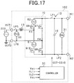
- FIG. 17 illustrates a circuit diagram of the power converter 100 in accordance with the second modification to the fourth embodiment.
- the first current sensor 61 may be connected between the source of the ninth switch Q 9 and the drain of the tenth switch Q 10 and provided on the opposite side of the fifth connection point K 5 from the ninth switch Q 9 .
- the second current sensor 62 may be provided on the drain side of the ninth switch Q 9 .
- FIG. 18 is a functional block diagram of the controller 30 of the second modification to the fourth embodiment. Also in the present modification, the controller 30 controls the DC-AC converter 10 using peak current mode control.
- the output terminal of the polarity switcher 55 is connected to the input terminal of the second AND circuit 383 and the gate of the eighth switch Q 8 , and the input terminal of the inverter 360 .
- the output terminal of the inverter 360 is connected to the input terminal of the first AND circuit 382 and the gate of the seventh switch Q 7 .
- the output signal of the RS flip-flop 357 of the first current controller 51 and the inverse of the output signal of the polarity switcher 55 are input to the first AND circuit 382 .
- the output terminal of the first AND circuit 382 is connected to the gate of the tenth switch Q 10 .
- the output signal of the RS flip-flop 357 of the second current controller 52 and the output signal of the polarity switcher 55 are input to the second AND circuit 383 .
- the output terminal of the second AND circuit 383 is connected to the gate of the ninth switch Q 9 .
- a signal output from the first AND circuit 382 to the gate of the tenth switch Q 10 is a tenth gate signal GS 10 .
- a signal output from the second AND circuit 383 to the gate of the ninth switch Q 9 is a ninth gate signal GS 9 .
- a signal output from the polarity switcher 55 via the inverter 360 to the gate of the seventh switch Q 7 is a seventh gate signal GS 7 .
- a signal output from the polarity switcher 55 to the gate of the eighth switch Q 8 is an eighth gate signal GS 8 .
- the HIGH output signal of the polarity switcher 55 leads to the HIGH eighth gate signal GS 8 and the LOW seventh gate signal GS 7 .
- the second current controller 52 uses peak current mode control, changes the ninth gate signal GS 9 from the HIGH state to the LOW state or from the LOW state to the HIGH state to control the second reactor current IL 2 r to the commanded current after correction ILa*.
- the LOW output signal of the polarity switcher 55 leads to the LOW eighth gate signal GS 8 and the HIGH seventh gate signal GS 7 .
- the first current controller 51 using peak current mode control, changes the tenth gate signal GS 10 from the HIGH state to the LOW state or from the LOW state to the HIGH state to control the first reactor current IL 1 r to the commanded current after correction ILa*.
- the current corrector 40 is configured to superimpose the current correction value Ic on the commanded current before correction IL* to calculate the commanded current after correction ILa*, thereby reducing distortions in the output current Iac.
- the seventh switch Q 7 may be normally in the open state during the first period P 1 and the ninth switch Q 9 may be normally in the open state during the second period P 2 .
- the seventh gate signal GS 7 may be kept in the LOW state during the first period P 1 and the ninth gate signal GS 9 may be kept in the LOW state during the second period P 2 .
- a fifth embodiment will now be described. Only differences of the fifth embodiment from the fourth embodiment will be described and description about the common configuration between the fifth and fourth embodiments is not provided in order to avoid repetition. Identical or equivalent components or components of equal or equivalent action are identified by the same or similar reference numerals.
- FIG. 19 is a circuit diagram of the DC-AC converter 10 in accordance with the fifth embodiment.
- an eleventh switch Q 11 and a twelfth switch Q 12 are provided between the first and second output terminals OUT 1 , OUT 2 and the full-bridge circuit 70 . More specifically, a source of the eleventh switch Q 11 and a source of the twelfth switch Q 12 are connected to each other. A drain of the eleventh switch Q 11 is connected to part of the fifth wiring LP 5 between the reactor 13 and the full-bridge circuit 70 . A drain of the twelfth switch Q 12 is connected to the sixth wiring LP 6 .
- Each of the eleventh and twelfth switches Q 11 , Q 12 has a parasitic diode connected in anti-parallel therewith.
- FIG. 20 is a functional block diagram of the controller 30 of the fifth embodiment. Also in the present embodiment, the controller 30 controls the DC-AC converter 10 using peak current mode control.
- the output terminal of the polarity switcher 55 is connected to the input terminal of the second AND circuit 383 , the gate of the twelfth switch Q 12 , and the input terminal of the inverter 360 .
- the output terminal of the inverter 360 is connected to the input terminal of the first AND circuit 382 and the gate of the eleventh switch Q 11 .
- the output terminal of the first AND circuit 382 is connected to the gate of each of the eighth and ninth switches Q 8 , Q 9 .
- the output terminal of the second AND circuit 383 is connected to the gate of each of the seventh and tenth switches Q 7 , Q 10 .
- a signal output from the first AND circuit 382 to the gate of the eighth switch Q 8 is an eighth gate signal GS 8 .
- a signal output from the first AND circuit 382 to the gate of the ninth switch Q 9 is a ninth gate signal GS 9 .
- a signal output from the second AND circuit 383 to the gate of the seventh switch Q 7 is a seventh gate signal GS 7 .
- a signal output from the second AND circuit 383 to the gate of the tenth switch Q 10 is a tenth gate signal GS 10 .
- a signal output from the polarity switcher 55 via the inverter 360 to the gate of the eleventh switch Q 11 is an eleventh gate signal GS 11 .
- a signal output from the polarity switcher 55 to the gate of the twelfth switch Q 12 is a twelfth gate signal GS 12 .
- FIG. 21 is a timing diagram for the DC-AC converter 10 of the fifth embodiment.
- FIG. 21( a ) illustrates an example of a change in each of the input voltage Vdc and the supply voltage Vac.
- FIG. 21( b ) illustrates an example of a change in each of the eighth and ninth gate signals GS 8 , GS 9 .
- FIG. 21( c ) illustrates an example of a change in each of the seventh and tenth gate signals GS 7 , GS 10 .
- FIG. 21( d ) illustrates an example of a change in the eleventh gate signal GS 11 .
- FIG. 21( e ) illustrates an example of a change in the twelfth gate signal GS 12 .
- FIG. 21( f ) illustrates an example of a change in the commanded current after correction ILa*.
- the HIGH twelfth gate signal GS 12 places the twelfth switch Q 12 in the closed state and the LOW eleventh gate signal GS 11 places the eleventh switch Q 11 in the open state.
- the first current controller 51 uses peak current mode control, changes each of the eighth and ninth gate signals GS 8 , GS 9 from the HIGH state to the LOW state or from the LOW state to the HIGH state to control the first reactor current IL 1 r to the commanded current after correction ILa*.
- the second current controller 52 uses peak current mode control, changes each of the seventh and tenth gate signals GS 7 , GS 10 from the HIGH state to the LOW state or from the LOW state to the HIGH state to control the second reactor current IL 2 r to the commanded current after correction ILa*.
- the current corrector 40 is configured to superimpose the current correction value Ic on the commanded current before correction IL* to calculate the commanded current after correction ILa*, thereby reducing distortions in the output current Iac.
- the present embodiment of the present disclosure can provide advantages similar to those of the first embodiment.
- the full-bridge circuit 12 may be a circuit formed of four insulated gate bipolar transistors (IGBTs).
- the second switch Q 2 may be formed of an IGBT or a diode.
Landscapes
- Engineering & Computer Science (AREA)
- Power Engineering (AREA)
- Rectifiers (AREA)
- Dc-Dc Converters (AREA)
- Inverter Devices (AREA)
Abstract
Description
Δi=IL*−Iave=Δslope+ΔIL/2 (1)
ΔIL=(Vdc−|Vac|)/L×D×Tsw (2)
where D represents a duty cycle of the first switch Q1 during the on-period.
Δslope=m×D×Tsw (3)
where m (A/s) represents an increase rate of the slope compensation signal Slope.
Claims (8)
Applications Claiming Priority (2)
| Application Number | Priority Date | Filing Date | Title |
|---|---|---|---|
| JP2018011001A JP6983082B2 (en) | 2018-01-25 | 2018-01-25 | DC / AC converter control device |
| JP2018-011001 | 2018-01-25 |
Publications (2)
| Publication Number | Publication Date |
|---|---|
| US20190229645A1 US20190229645A1 (en) | 2019-07-25 |
| US10637370B2 true US10637370B2 (en) | 2020-04-28 |
Family
ID=67145347
Family Applications (1)
| Application Number | Title | Priority Date | Filing Date |
|---|---|---|---|
| US16/253,699 Active US10637370B2 (en) | 2018-01-25 | 2019-01-22 | Apparatus for controlling DC-AC converter to reduce distortions in output current |
Country Status (4)
| Country | Link |
|---|---|
| US (1) | US10637370B2 (en) |
| JP (1) | JP6983082B2 (en) |
| CN (1) | CN110086367B9 (en) |
| DE (1) | DE102019101566A1 (en) |
Cited By (2)
| Publication number | Priority date | Publication date | Assignee | Title |
|---|---|---|---|---|
| US10910958B2 (en) * | 2018-11-28 | 2021-02-02 | Denso Corporation | Control apparatus for power conversion system |
| US20220045595A1 (en) * | 2019-04-25 | 2022-02-10 | Denso Corporation | Control apparatus for power conversion apparatus |
Families Citing this family (4)
| Publication number | Priority date | Publication date | Assignee | Title |
|---|---|---|---|---|
| JP6913056B2 (en) * | 2018-05-29 | 2021-08-04 | 株式会社Soken | Power converter control device |
| JP7161447B2 (en) | 2019-06-24 | 2022-10-26 | 株式会社Soken | power converter |
| CN111953199A (en) * | 2020-07-31 | 2020-11-17 | 海信(山东)空调有限公司 | PFC converter, feedforward control method and device thereof and air conditioner |
| LU102123B1 (en) * | 2020-10-09 | 2022-04-11 | Phoenix Contact Gmbh & Co | Boost converter circuitry, power supply and method for stepping up an input voltage |
Citations (12)
| Publication number | Priority date | Publication date | Assignee | Title |
|---|---|---|---|---|
| US6545887B2 (en) * | 1999-08-06 | 2003-04-08 | The Regents Of The University Of California | Unified constant-frequency integration control of three-phase power factor corrected rectifiers, active power filters and grid-connected inverters |
| US20130301323A1 (en) * | 2012-05-10 | 2013-11-14 | Denso Corporation | Power conversion apparatus |
| US20140029308A1 (en) * | 2011-03-09 | 2014-01-30 | Solantro Semiconductor Corp. | Inverter having extended lifetime dc-link capacitors |
| US20140198538A1 (en) * | 2013-01-16 | 2014-07-17 | Nippon Soken, Inc. | Power converter with current feedback loop |
| US20140361720A1 (en) * | 2013-06-05 | 2014-12-11 | Denso Corporation | Apparatus for controlling rotating machine based on output signal of resolver |
| US20150280591A1 (en) * | 2014-03-28 | 2015-10-01 | Denso Corporation | Power conversion apparatus |
| JP2015198460A (en) | 2014-03-31 | 2015-11-09 | 株式会社デンソー | Power conversion device |
| US20160094134A1 (en) * | 2014-09-25 | 2016-03-31 | Denso Corporation | Power conversion apparatus |
| JP2016192889A (en) | 2015-03-30 | 2016-11-10 | パナソニックIpマネジメント株式会社 | Power converter |
| US9590484B2 (en) * | 2014-02-26 | 2017-03-07 | Fsp Technology Inc. | Inverter device and power converting method thereof |
| US20170302161A1 (en) * | 2016-04-15 | 2017-10-19 | Emerson Climate Technologies, Inc. | Input Reference Signal Generation Systems And Methods |
| US20180269779A1 (en) * | 2017-03-20 | 2018-09-20 | Silergy Semiconductor Technology (Hangzhou) Ltd | Power factor correction circuit, control method and controller |
Family Cites Families (4)
| Publication number | Priority date | Publication date | Assignee | Title |
|---|---|---|---|---|
| JPS6051470A (en) * | 1983-08-30 | 1985-03-22 | Yamaha Motor Co Ltd | Inverter device |
| JP3316735B2 (en) * | 1996-05-16 | 2002-08-19 | 三菱電機株式会社 | Grid-connected inverter device |
| WO2006064586A1 (en) * | 2004-12-15 | 2006-06-22 | Fujitsu General Limited | Power supply apparatus |
| CN101976958B (en) * | 2010-11-10 | 2012-08-01 | 电子科技大学 | High-efficiency power regulating device based on power factor correction |
-
2018
- 2018-01-25 JP JP2018011001A patent/JP6983082B2/en active Active
-
2019
- 2019-01-22 US US16/253,699 patent/US10637370B2/en active Active
- 2019-01-23 DE DE102019101566.9A patent/DE102019101566A1/en active Pending
- 2019-01-24 CN CN201910068042.1A patent/CN110086367B9/en active Active
Patent Citations (12)
| Publication number | Priority date | Publication date | Assignee | Title |
|---|---|---|---|---|
| US6545887B2 (en) * | 1999-08-06 | 2003-04-08 | The Regents Of The University Of California | Unified constant-frequency integration control of three-phase power factor corrected rectifiers, active power filters and grid-connected inverters |
| US20140029308A1 (en) * | 2011-03-09 | 2014-01-30 | Solantro Semiconductor Corp. | Inverter having extended lifetime dc-link capacitors |
| US20130301323A1 (en) * | 2012-05-10 | 2013-11-14 | Denso Corporation | Power conversion apparatus |
| US20140198538A1 (en) * | 2013-01-16 | 2014-07-17 | Nippon Soken, Inc. | Power converter with current feedback loop |
| US20140361720A1 (en) * | 2013-06-05 | 2014-12-11 | Denso Corporation | Apparatus for controlling rotating machine based on output signal of resolver |
| US9590484B2 (en) * | 2014-02-26 | 2017-03-07 | Fsp Technology Inc. | Inverter device and power converting method thereof |
| US20150280591A1 (en) * | 2014-03-28 | 2015-10-01 | Denso Corporation | Power conversion apparatus |
| JP2015198460A (en) | 2014-03-31 | 2015-11-09 | 株式会社デンソー | Power conversion device |
| US20160094134A1 (en) * | 2014-09-25 | 2016-03-31 | Denso Corporation | Power conversion apparatus |
| JP2016192889A (en) | 2015-03-30 | 2016-11-10 | パナソニックIpマネジメント株式会社 | Power converter |
| US20170302161A1 (en) * | 2016-04-15 | 2017-10-19 | Emerson Climate Technologies, Inc. | Input Reference Signal Generation Systems And Methods |
| US20180269779A1 (en) * | 2017-03-20 | 2018-09-20 | Silergy Semiconductor Technology (Hangzhou) Ltd | Power factor correction circuit, control method and controller |
Cited By (3)
| Publication number | Priority date | Publication date | Assignee | Title |
|---|---|---|---|---|
| US10910958B2 (en) * | 2018-11-28 | 2021-02-02 | Denso Corporation | Control apparatus for power conversion system |
| US20220045595A1 (en) * | 2019-04-25 | 2022-02-10 | Denso Corporation | Control apparatus for power conversion apparatus |
| US11923756B2 (en) * | 2019-04-25 | 2024-03-05 | Denso Corporation | Control apparatus for power conversion apparatus |
Also Published As
| Publication number | Publication date |
|---|---|
| CN110086367A (en) | 2019-08-02 |
| JP6983082B2 (en) | 2021-12-17 |
| CN110086367B (en) | 2023-10-03 |
| CN110086367B9 (en) | 2023-11-28 |
| JP2019129652A (en) | 2019-08-01 |
| DE102019101566A1 (en) | 2019-07-25 |
| US20190229645A1 (en) | 2019-07-25 |
Similar Documents
| Publication | Publication Date | Title |
|---|---|---|
| US10637370B2 (en) | Apparatus for controlling DC-AC converter to reduce distortions in output current | |
| US20120300519A1 (en) | Multi-phase active rectifier | |
| US9634602B2 (en) | Three-phase inverter apparatus and control method thereof | |
| US10541638B2 (en) | Control apparatus and control method | |
| US10910958B2 (en) | Control apparatus for power conversion system | |
| US10615680B2 (en) | Control apparatus for power converter | |
| US11183944B2 (en) | Control apparatus for power converter | |
| US11923756B2 (en) | Control apparatus for power conversion apparatus | |
| TW200414660A (en) | Pulse width modulation method and device thereof, power conversion method and power converter | |
| CN117394735A (en) | Inverter dead zone compensation method and system | |
| WO2019097835A1 (en) | Power conversion device | |
| WO2017033428A1 (en) | Power conversion device | |
| US11418128B2 (en) | Control apparatus for electric power conversion apparatus | |
| JP6540315B2 (en) | Power converter | |
| US11245326B2 (en) | Control apparatus for electrical power converter | |
| CN113273072B (en) | Control device for DC/AC conversion device | |
| JP2022090317A (en) | Inverter control device, and control method of inverter | |
| JP3397138B2 (en) | Inverter device | |
| JP6993925B2 (en) | Power converter control device | |
| JP2000014014A (en) | Inverter device | |
| JP2000270563A (en) | Control circuit for power converter | |
| JP2015089265A (en) | Control device and control method of converter, and air conditioner | |
| CN116391317A (en) | Power conversion system | |
| JP2020115719A (en) | Power control method and power controller | |
| JPH10323054A (en) | Control method for pulse width modulated inverter |
Legal Events
| Date | Code | Title | Description |
|---|---|---|---|
| FEPP | Fee payment procedure |
Free format text: ENTITY STATUS SET TO UNDISCOUNTED (ORIGINAL EVENT CODE: BIG.); ENTITY STATUS OF PATENT OWNER: LARGE ENTITY |
|
| AS | Assignment |
Owner name: DENSO CORPORATION, JAPAN Free format text: ASSIGNMENT OF ASSIGNORS INTEREST;ASSIGNORS:IYASU, SEIJI;HAYASHI, YUJI;HANDA, YUICHI;SIGNING DATES FROM 20190130 TO 20190205;REEL/FRAME:049042/0812 |
|
| STPP | Information on status: patent application and granting procedure in general |
Free format text: NON FINAL ACTION MAILED |
|
| STPP | Information on status: patent application and granting procedure in general |
Free format text: RESPONSE TO NON-FINAL OFFICE ACTION ENTERED AND FORWARDED TO EXAMINER |
|
| STPP | Information on status: patent application and granting procedure in general |
Free format text: NOTICE OF ALLOWANCE MAILED -- APPLICATION RECEIVED IN OFFICE OF PUBLICATIONS |
|
| STCF | Information on status: patent grant |
Free format text: PATENTED CASE |
|
| MAFP | Maintenance fee payment |
Free format text: PAYMENT OF MAINTENANCE FEE, 4TH YEAR, LARGE ENTITY (ORIGINAL EVENT CODE: M1551); ENTITY STATUS OF PATENT OWNER: LARGE ENTITY Year of fee payment: 4 |