US10594217B2 - Asymmetric two-stage DC-DC switching converter - Google Patents
Asymmetric two-stage DC-DC switching converter Download PDFInfo
- Publication number
- US10594217B2 US10594217B2 US15/278,492 US201615278492A US10594217B2 US 10594217 B2 US10594217 B2 US 10594217B2 US 201615278492 A US201615278492 A US 201615278492A US 10594217 B2 US10594217 B2 US 10594217B2
- Authority
- US
- United States
- Prior art keywords
- stage
- phases
- asymmetric
- power converter
- switching
- Prior art date
- Legal status (The legal status is an assumption and is not a legal conclusion. Google has not performed a legal analysis and makes no representation as to the accuracy of the status listed.)
- Active
Links
Images


Classifications
-
- H—ELECTRICITY
- H02—GENERATION; CONVERSION OR DISTRIBUTION OF ELECTRIC POWER
- H02M—APPARATUS FOR CONVERSION BETWEEN AC AND AC, BETWEEN AC AND DC, OR BETWEEN DC AND DC, AND FOR USE WITH MAINS OR SIMILAR POWER SUPPLY SYSTEMS; CONVERSION OF DC OR AC INPUT POWER INTO SURGE OUTPUT POWER; CONTROL OR REGULATION THEREOF
- H02M3/00—Conversion of dc power input into dc power output
- H02M3/02—Conversion of dc power input into dc power output without intermediate conversion into ac
- H02M3/04—Conversion of dc power input into dc power output without intermediate conversion into ac by static converters
- H02M3/10—Conversion of dc power input into dc power output without intermediate conversion into ac by static converters using discharge tubes with control electrode or semiconductor devices with control electrode
- H02M3/145—Conversion of dc power input into dc power output without intermediate conversion into ac by static converters using discharge tubes with control electrode or semiconductor devices with control electrode using devices of a triode or transistor type requiring continuous application of a control signal
- H02M3/155—Conversion of dc power input into dc power output without intermediate conversion into ac by static converters using discharge tubes with control electrode or semiconductor devices with control electrode using devices of a triode or transistor type requiring continuous application of a control signal using semiconductor devices only
- H02M3/156—Conversion of dc power input into dc power output without intermediate conversion into ac by static converters using discharge tubes with control electrode or semiconductor devices with control electrode using devices of a triode or transistor type requiring continuous application of a control signal using semiconductor devices only with automatic control of output voltage or current, e.g. switching regulators
- H02M3/158—Conversion of dc power input into dc power output without intermediate conversion into ac by static converters using discharge tubes with control electrode or semiconductor devices with control electrode using devices of a triode or transistor type requiring continuous application of a control signal using semiconductor devices only with automatic control of output voltage or current, e.g. switching regulators including plural semiconductor devices as final control devices for a single load
- H02M3/1582—Buck-boost converters
-
- H—ELECTRICITY
- H02—GENERATION; CONVERSION OR DISTRIBUTION OF ELECTRIC POWER
- H02M—APPARATUS FOR CONVERSION BETWEEN AC AND AC, BETWEEN AC AND DC, OR BETWEEN DC AND DC, AND FOR USE WITH MAINS OR SIMILAR POWER SUPPLY SYSTEMS; CONVERSION OF DC OR AC INPUT POWER INTO SURGE OUTPUT POWER; CONTROL OR REGULATION THEREOF
- H02M1/00—Details of apparatus for conversion
- H02M1/14—Arrangements for reducing ripples from dc input or output
-
- H—ELECTRICITY
- H02—GENERATION; CONVERSION OR DISTRIBUTION OF ELECTRIC POWER
- H02M—APPARATUS FOR CONVERSION BETWEEN AC AND AC, BETWEEN AC AND DC, OR BETWEEN DC AND DC, AND FOR USE WITH MAINS OR SIMILAR POWER SUPPLY SYSTEMS; CONVERSION OF DC OR AC INPUT POWER INTO SURGE OUTPUT POWER; CONTROL OR REGULATION THEREOF
- H02M1/00—Details of apparatus for conversion
- H02M1/36—Means for starting or stopping converters
-
- H—ELECTRICITY
- H02—GENERATION; CONVERSION OR DISTRIBUTION OF ELECTRIC POWER
- H02M—APPARATUS FOR CONVERSION BETWEEN AC AND AC, BETWEEN AC AND DC, OR BETWEEN DC AND DC, AND FOR USE WITH MAINS OR SIMILAR POWER SUPPLY SYSTEMS; CONVERSION OF DC OR AC INPUT POWER INTO SURGE OUTPUT POWER; CONTROL OR REGULATION THEREOF
- H02M3/00—Conversion of dc power input into dc power output
- H02M3/02—Conversion of dc power input into dc power output without intermediate conversion into ac
- H02M3/04—Conversion of dc power input into dc power output without intermediate conversion into ac by static converters
- H02M3/10—Conversion of dc power input into dc power output without intermediate conversion into ac by static converters using discharge tubes with control electrode or semiconductor devices with control electrode
- H02M3/145—Conversion of dc power input into dc power output without intermediate conversion into ac by static converters using discharge tubes with control electrode or semiconductor devices with control electrode using devices of a triode or transistor type requiring continuous application of a control signal
- H02M3/155—Conversion of dc power input into dc power output without intermediate conversion into ac by static converters using discharge tubes with control electrode or semiconductor devices with control electrode using devices of a triode or transistor type requiring continuous application of a control signal using semiconductor devices only
- H02M3/156—Conversion of dc power input into dc power output without intermediate conversion into ac by static converters using discharge tubes with control electrode or semiconductor devices with control electrode using devices of a triode or transistor type requiring continuous application of a control signal using semiconductor devices only with automatic control of output voltage or current, e.g. switching regulators
- H02M3/158—Conversion of dc power input into dc power output without intermediate conversion into ac by static converters using discharge tubes with control electrode or semiconductor devices with control electrode using devices of a triode or transistor type requiring continuous application of a control signal using semiconductor devices only with automatic control of output voltage or current, e.g. switching regulators including plural semiconductor devices as final control devices for a single load
- H02M3/1584—Conversion of dc power input into dc power output without intermediate conversion into ac by static converters using discharge tubes with control electrode or semiconductor devices with control electrode using devices of a triode or transistor type requiring continuous application of a control signal using semiconductor devices only with automatic control of output voltage or current, e.g. switching regulators including plural semiconductor devices as final control devices for a single load with a plurality of power processing stages connected in parallel
-
- H—ELECTRICITY
- H02—GENERATION; CONVERSION OR DISTRIBUTION OF ELECTRIC POWER
- H02M—APPARATUS FOR CONVERSION BETWEEN AC AND AC, BETWEEN AC AND DC, OR BETWEEN DC AND DC, AND FOR USE WITH MAINS OR SIMILAR POWER SUPPLY SYSTEMS; CONVERSION OF DC OR AC INPUT POWER INTO SURGE OUTPUT POWER; CONTROL OR REGULATION THEREOF
- H02M1/00—Details of apparatus for conversion
- H02M1/0067—Converter structures employing plural converter units, other than for parallel operation of the units on a single load
- H02M1/007—Plural converter units in cascade
-
- H—ELECTRICITY
- H02—GENERATION; CONVERSION OR DISTRIBUTION OF ELECTRIC POWER
- H02M—APPARATUS FOR CONVERSION BETWEEN AC AND AC, BETWEEN AC AND DC, OR BETWEEN DC AND DC, AND FOR USE WITH MAINS OR SIMILAR POWER SUPPLY SYSTEMS; CONVERSION OF DC OR AC INPUT POWER INTO SURGE OUTPUT POWER; CONTROL OR REGULATION THEREOF
- H02M1/00—Details of apparatus for conversion
- H02M1/0067—Converter structures employing plural converter units, other than for parallel operation of the units on a single load
- H02M1/008—Plural converter units for generating at two or more independent and non-parallel outputs, e.g. systems with plural point of load switching regulators
-
- H02M2001/007—
-
- H02M2001/008—
Definitions
- the disclosure relates generally to a DC-DC switching power converter, employing multiple stages and multiple phases.
- Asymmetric switching converter architectures have been presented in related patent application Ser. No. 14/052,844, Ser. No. 15/189,210, and Ser. No. 15/263,732. These architectures provide benefits by optimizing different phases for different operating conditions and then controlling which phases are operated depending on the load condition.
- patent application Ser. No. 14/052,844 describes how different inductors can be chosen to provide either better efficiency at low load, or higher performance (load transient response) for high loads.
- Patent application Ser. No. 15/189,210 shows how peak-mode phases and valley-mode phases may be combined to simplify the implementation of low-load discontinuous-mode, while allowing faster switching frequencies for the high-load phases, than would be possible using peak-mode architecture.
- An object of the disclosure is to provide an asymmetric two-stage DC-DC switching power converter with very high low-load efficiency and extremely high transient response at high-load.
- Another object of this disclosure is the design of a two-stage DC-DC switching power converter that combines low switching frequency single-stage phases for low-load operation, and high switching frequency two-stage phases for high-load operation.
- Another object of this disclosure is to control the second-stage phases of a DC-DC switching power converter with little or no information from the rest of the system, such that the second-stage phases operate effectively, disabling at low loads, and ramping their output current up smoothly, as the switching converter load is increased.
- Another object of this disclosure is to control the second-stage phases of a DC-DC switching power converter using a separate control scheme from the first stage phases, operating the switching converter with finite DC output impedance, and providing current from local and remote phases, with good control over the relative currents from each phase.
- a still further object is to auto-calibrate the second stage-phases of a DC-DC switching power converter during startup to remove any offsets in the system, allowing local and remote control loops to be used together without issue, and to use either the output voltage of the switching converter just after startup, or the intermediate voltage, as a reference voltage against which the second-stage phases are calibrated, and providing a window during which auto-calibration is completed.
- a DC-DC switching converter comprised of a Buck, Boost, or Buck-Boost, configured for more than one phase of operation.
- the switching converter requires that some of the phases operate as a single-stage, regulating directly from the supply voltage down to the output voltage.
- the switching converter requires that some of the phases operate in a two-stage, or multi-stage, configuration regulating to an intermediate voltage, and then down to the output voltage.
- the switching converter is configured for single-stage phases operating at low switching frequencies and low loads.
- the switching converter is configured for two-stage phases operating at high switching frequencies and high loads.
- Optional auto-calibration is configured, to match the references of different stages, whether single stage or multi-stage, for a seamless multi-phase operation, when all the phases of all the stages are combined to deliver current.
- the above and other objects are further achieved by a method for operating an asymmetric two-stage DC-DC switching converter.
- the steps include providing more than one phase, where one or more multi-stage phases, are in parallel with one or more single-stage phases.
- a single control signal controls the single-stage and multi-stage phases.
- An intermediate voltage, between a first and second stage of one or more multi-stage phases, is provided.
- the objects may be achieved by implementing a number of single-stage phases, some using peak-mode and some using valley-mode control, with some of two-stage phases operating from a single first-stage phase providing a common intermediate voltage, and a further two-stage phase operating from another first-stage phase providing a separate intermediate voltage.
- the objects may be achieved by implementing a single first-stage switching converter providing an intermediate output voltage rail to multiple second-stage switching converters, where the second-stage switching converters are partitioned to provide power to different regulated outputs.
- the objects may be achieved by implementing a control signal that is a single-ended voltage, a single-ended current, or a number of currents one for each phase to be controlled.
- the objects may be achieved by implementing the output voltage of the DC-DC switching converter as a reference voltage against which the second-stage phases are calibrated to remove any offsets in the system.
- the objects may be achieved by implementing the intermediate voltage of the DC-DC switching converter as a reference voltage against which the second-stage phases are calibrated to remove any offsets in the system.
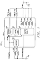
- FIG. 1 illustrates two single-stage phases operating at low load conditions, and a set of very fast phases operating at high load conditions, operated from a lower value intermediate voltage, provided by a first-stage Buck switching converter, embodying the principles of the disclosure.
- FIG. 2 shows a more general implementation, embodying the principles of the disclosure.
- FIG. 3 illustrates a single first-stage Buck switching converter providing an intermediate output voltage rail to multiple second-stage high frequency Buck switching converters, embodying the principles of the disclosure.
- FIG. 4 shows a system where at least some of the second-stage phases are located remotely from the single-stage and first-stage phases, embodying the principles of the disclosure.
- FIG. 5 illustrates a common control signal system, with a DAC and amplifier providing the control signal to all phases, distributed as a dual-ended voltage signal, embodying the principles of the disclosure.
- FIG. 6 shows a system where at least some of the phases are located on a separate silicon die, allowing each part of the switching converter to be optimized for operating conditions, embodying the principles of the disclosure.
- FIG. 7 illustrates an ideal two-chip solution, though not making use of the disclosure as described below, where the two chips are essentially separate systems, and the two DACs are not adequately well matched.
- FIG. 8 shows the overall trans-conductance of the switching converter and the contributions from the local and the remote phases, embodying the principles of the disclosure.
- FIG. 9 illustrates a simplified system, where the master phases provide the single-stage phases and the first-stage “pre-regulator” phases for the two-stage phases, embodying the principles of the disclosure.
- FIG. 10 shows a timing diagram for the calibration window where the DAC voltage of the second-stage phases is calibrated to match the output voltage, embodying the principles of the disclosure.
- FIG. 11 illustrates a variant of the system, where the auto-calibration uses a voltage derived from the intermediate voltage, embodying the principles of the disclosure.
- FIG. 12 is a flow chart of a method for an asymmetric two-stage DC-DC switching converter, for converting an input voltage to an output voltage, embodying the principles of the disclosure.
- An asymmetric two-stage DC-DC switching power converter with very high low-load efficiency and extremely high transient response at high-load is proposed.
- the proposal combines low-switching frequency single-stage phases, for low load operation, with high-switching frequency two-stage phases, for high load operation.
- asymmetrical multiphase converter architecture is that each phase type is optimized for a narrower operating condition. This allows for improved system performance and operating efficiency.
- the proposal highlights the benefits of adding a dual-stage switching converter stage(s) in parallel with a single-stage switching converter stage(s), within the asymmetrical multiphase converter architecture.
- the dual stage phase consists of a lower frequency first stage, responsible of stepping down the input voltage to an intermediate voltage rail.
- the second stage is a high frequency switching converter responsible for stepping down the intermediate voltage to a regulated output voltage desired by the load.
- FIG. 1 illustrates 100 , two single-stage phases operating at low load conditions, and a set of very fast phases operating at high load conditions, operated from a lower value intermediate voltage, provided by a first-stage Buck switching converter, embodying the principles of the disclosure.
- the asymmetrical multiphase converter architecture provides improved over-all system performance by providing optimized phases, for specific operating conditions and by controlling which phases are active based on the current operating conditions.
- the principle benefit is the lower ratio between the intermediate voltage rail V_INTERMEDIATE across capacitor 115 , and the final regulated output voltage V_OUT across capacitor 175 , allowing the second-stage switching converter to operate at a greater switching frequency due to the higher ON-time to OFF-time duty cycle.
- the major benefits of high frequency switching are improved dynamic load response, smaller inductor values and filter components, and improved output ripple characteristics.
- MASTER 130 operates at low load conditions.
- MASTER 130 operates from supply V_SUPPLY, and INTER 135 . They typically operate at relatively low switching frequencies, and with relatively large value inductors 165 and 170 .
- a set of very fast phases, SLAVES 140 is then operated only at high load conditions. These are operated at much higher switching frequencies and with much smaller value inductors 145 , 150 155 , and 160 .
- SLAVES 140 control is from lower value intermediate voltage, V_INTERMEDIATE, regulated down from V_SUPPLY, through first stage switching converter SUPPORT 125 , and inductors 105 and 110 .
- the coordination between the control elements of the switching converter phases may be carried forward in regards to the dual-stage phases.
- the same control signal that controls the output of the single-stage phases may provide the control for the second stage of the two-stage phases.
- the same peak-current signal may be used for all the single-stage phases and for all the second stages of the two-stage phases.
- control elements include the control elements of both the first-stage and second-stage switching converters.
- the intermediate voltage rail, output of the first switching converter stage may be increased or decreased, depending on the current operating condition.
- FIG. 2 shows a more general implementation in 200 , embodying the principles of the disclosure.
- a number of single-stage phases are provided, some using peak-mode and some using valley-mode control, using a variety of frequencies and inductor values, as further described in related patent application Ser. No. 15/189,210.
- PHASE 0 and PHASE 1 typically operate at relatively low switching frequencies, and with relatively large value inductors 224 and 223 .
- PHASE 2 and PHASE 3 typically operate at much higher switching frequencies and with much smaller value inductors 222 and 221 .
- PHASE 0 , PHASE 1 , PHASE 2 , and PHASE 3 operate from supply V_IN.
- a pair of two-stage phases are provided in PHASE 4 and PHASE 5 , operating from a single first-stage phase PHASE 4 / 5 , providing a common intermediate voltage V_INTERMEDIATE across inductor 212 .
- PHASE 4 and PHASE 5 typically operate at very high switching frequencies and very small value inductors 215 and 214 .
- a further two-stage phase is also provided in PHASE 6 which operates from another first-stage, providing a separate intermediate voltage across inductor 211 .
- PHASE 4 / 5 operates from supply V_IN, and output voltage V_OUT is across capacitor 230 .
- low, high, and very high refers to switching frequencies, inductor sizes, and the like, and is meant to be in comparison to other components of the same type, such as converter phases or stages, or inductors, that are connected to other phases or stages, in the same system.
- FIG. 3 300 illustrates a single first-stage Buck switching converter providing an intermediate output voltage rail to multiple second-stage high frequency Buck switching converters, embodying the principles of the disclosure.
- Input voltage V_IN supplies first-stage 310 , which in turn provides a common intermediate voltage V_INTERMEDIATE across inductor 327 , to second stages 315 , 317 , 319 , and 321 .
- Input voltage V_IN also supplies single-stage phases 311 , 313 , 323 , and 325 .
- V_OUT 1 is provided through inductors 312 and 314 , from single-stages 311 and 313 respectively, and V_OUT 2 through inductors 324 and 326 , from single-stages 323 and 325 .
- Second-stage buck converters, 315 , 317 , 319 , and 321 are partitioned to provide power to different regulated outputs.
- V_OUT 1 is provided through inductors 316 and 318 , from second stages 315 and 317 respectively, and V_OUT 2 through inductors 320 and 322 , from second stages 319 and 321 .
- several multi-phase converters are used to provide multiple regulated outputs.
- Communication is provided between the control elements of each of the switching converters.
- the load devices require the multi-phase switching converter to respond to extreme operating conditions, such as dynamic load, and system limitations, such as component height limitation.
- system limitations such as component height limitation.
- FIG. 4 shows system 400 , where at least some of the second-stage phases are located remotely from the single-stage and first stage phases, embodying the principles of the disclosure.
- input voltage V_IN supplies first-stage phase 405 , which in turn supplies second stages 421 and 423 , with a common intermediate voltage V_INTERMEDIATE across inductor 406 .
- Input voltage V_IN also supplies single-stage phases 401 and 403 , which in turn provide V_OUT across inductors 402 and 404 , respectively.
- V_OUT is read at capacitor 425 and the point of the load.
- Second-stage phases 420 are located remotely from single-stage and first stage phases 410 . It may be advantageous to locate high frequency second-stage phases 421 and 423 , and their respective inductors 422 and 424 , away from the switching converter first stage phase, and in close proximity to the actual load device. Note that V_OUT is also read at inductors 422 and 424 , at capacitor 425 and the point of the load.
- any control signal it is beneficial for any control signal to be transmitted as a dual-ended, differential, signal as this is more immune to noise injection. It is also beneficial to add any fast output detection at the remote location. For example, a fast comparator may be used to monitor the output voltage. If the output voltage falls suddenly or falls outside the normal regulation window, then the comparator flags this and the switching converter responds quickly in some way. If this fast response system is used, then it is beneficial for the control signal to be implemented at the remote location.
- a fast comparator may be used to monitor the output voltage. If the output voltage falls suddenly or falls outside the normal regulation window, then the comparator flags this and the switching converter responds quickly in some way. If this fast response system is used, then it is beneficial for the control signal to be implemented at the remote location.
- the remote phases must have information about the state of the local phases and vice-versa. This is most conveniently achieved by using a common control signal for all single-stage, first-stage, and second-stage phases.
- a common control signal for all single-stage, first-stage, and second-stage phases.
- FIG. 5 illustrates a common control signal system 500 , with a DAC and amplifier providing a control signal to all phases, distributed as a dual-ended voltage signal, embodying the principles of the disclosure.
- Control block 510 is comprised of DAC 512 and amplifier 514 .
- the amplifier implements the basic control loop, setting the overall transconductance of the system and the main response shaping.
- Other ways of distributing the control signal are possible, such as a single-ended voltage, a single ended current, or a number of currents one for each phase to be controlled.
- control block 510 is responsible for keeping all phases controlled with a common dual-ended control signal.
- This logic may be implemented in either the remote die with SLAVE 540 , or the local die with MASTER 530 , or in a separate location such as SUPPORT 520 .
- SUPPORT 520 operates from separate DAC 522 , providing intermediate voltage, V_INTERMEDIATE across capacitor 550 , and is comprised of first stage switching converter 524 and SUPPORT PHASES logic 526 .
- Local MASTER 530 operates from DAC 512 at low load conditions and low switching frequencies, providing output voltage V_OUT across capacitor 560 , and is comprised of switching converter 532 , and MASTER PHASES logic 534 .
- Remote SLAVE 540 operates from DAC 512 at high load conditions and higher switching frequencies, providing output voltage V_OUT across capacitor 560 , and is comprised of switching converter 542 , and MASTER PHASES logic 544 .
- the switching converter may be implemented using two different silicon technologies. This may be particularly advantageous if the silicon process of the die containing the single-stage phases is unable to support the switching frequencies of the second-stage phases. In this case, the process is asymmetric, and optimized for the phases that it supports.
- FIG. 6 shows system 600 , where at least some of the phases are located on a separate silicon die, allowing each part of the switching converter to be optimized for operating conditions, embodying the principles of the disclosure.
- PMIC 1 610 which contains MASTER 612 configured to inductor 614 , and intermediate phases INTER 616 configured to inductor 618 , for low load conditions and large value inductors, is implemented using a slow, large-feature size and cheap process. It is likely that this process is not suitable for, or cannot support, the high switching frequency of the slave phases.
- PMIC 2 620 which contains slave phases SLAVE 1 622 configured to inductor 624 , and SLAVE 2 626 configured to inductor 628 , for higher switching frequencies and much smaller value inductors, is implemented using a faster, small-feature size and expensive process.
- Output voltage V_OUT, of the asymmetric two-stage switching converter, is across capacitor 630 .
- the present disclosure describes a way of implementing a control scheme for the remote phases that allows them to operate independently from the main phases, and still regulate correctly in the switching converter system. Specifically the disclosure details how offsets between the remote and main phases can be reduced or eliminated.
- the remote phases can be controlled with little or no information from the rest of the system, such that the remote phases operate effectively, disabling at low loads, and ramping their output current up smoothly, as the switching converter load is increased.
- the remote phases of the disclosure use a separate control scheme from the local phases, operating the switching converter with finite DC output impedance, and providing current from local and remote phases, with good control over the relative currents from each phase.
- the remote phases can be auto-calibrated during startup to remove any offsets in the system, allowing local and remote control loops to be used together without issue, and using either the output voltage of the switching converter just after startup, or the intermediate voltage, as a reference voltage against which the remote phases are calibrated, providing a window during which auto-calibration is completed.
- control signal in this case a dual-ended differential voltage
- the interconnect may be difficult given the application, and the ability to run the remote phases as a separate system is highly desirable.
- the preferred embodiment is operating a switching converter with multiple phases. Some of these phases are single-stage and some of the phases are two-stage.
- the single-stage phases are instantiated locally, within the PMIC.
- the first stages of the two-stage phases are also instantiated locally within the PMIC. These are controlled using a local control loop.
- the second stages of the two-stage phases are instantiated at a remote location. These stages are controlled using their own independent control loop.
- FIG. 7 illustrates an ideal two-chip solution 700 , though not making use of the disclosure as described below, where the two chips are essentially separate systems, and the two DACs are not adequately well matched.
- Master block 710 contains the single-stage phases and the support phases that generate the intermediate voltages in 713 and 718 .
- This block contains DAC 711 to set the target voltages for the master phases.
- amplifiers 714 and 715 which compare the output voltages, across capacitor 730 and capacitor 740 respectively, to the target voltage.
- the output of the amplifiers is used in control blocks 712 and 717 , to determine the duty-cycle of the switching converting on a cycle-by-cycle basis.
- the slave phases, in second stage 720 of the two-phases, are placed remotely from the master block.
- the slave phases have DAC 721 to provide a local target voltage.
- the slave phases also have comparators 724 and 725 , which prevent the slave phases from being active in control 722 , until V_OUT is 5 mV below the target voltage. In the actual system, this is impractical, as the two DAC blocks are not adequately well matched.
- the switching converter functions as follows. At very low loads, the single-stage phases switch independently, and the remote phases do not switch. Once the load is increased beyond a threshold level, the remote phases begin to switch. The current that the remote phases supply increases as the overall load increases.
- the current in all the phases relative to each other are well controlled, such that as the current rises in all the phases, all the phases reach maximum output current at the same point. This can be achieved if all the phases are controlled using a single control block, controlling every phase and having knowledge of the state of every phase. However if interconnect is to be minimized, it can be beneficial not to route control signals between the locations of the local and remote phases of the switching converter.
- An alternative system implements the remote phases as a separate system to the local phases of the switching converter.
- each location is provided with a separate DAC to create a locally generated target voltage.
- the switching converter has finite DC output impedance, and the output voltage falls proportionally to the load current. In this way, as the switching converter is loaded, the phases will increase their output current together.
- FIG. 8 shows 800 , the overall trans-conductance of the switching converter and the contributions from the local and the remote phases, embodying the principles of the disclosure.
- the first panel shows output voltage, VOUT.
- Target voltage VTARGET for the switching converter is indicated, as well as lower threshold VOFFSET, the target voltage for the remote phases.
- the second panel shows load current IOUT. As the load current increases to a maximum IMAX, the output voltage falls. Initially only the local phases are active and supply all the load current, in ILOCAL. Once the load is sufficient, the remote phases are enabled in IREMOTE. Both the local and the remote phases then supply the load, where the maximum local and remote currents reach IMAX_LOCAL and IMAX_REMOTE respectively.
- any offsets between the local and remote sites will cause the switching converter to operate in a way that is non-optimal. If, for example, the switching converter has an effective output impedance of 5 mOhm, a typical offset of 10 mV between the local and remote DACs could equate to a 2 A offset in phase currents.
- the most basic implementation of this scheme is as follows.
- the single stage phases are started without starting the first-stage pre-regulator of the two-stage phases, so that the intermediate voltage is not yet present. No load is present at this point.
- the single stage phases settle, and the output is set to the unloaded voltage of the switching converter. Any offsets in the single-stage phases are present in the output voltage.
- the first-stage phases are enabled and the intermediate voltage charged up.
- the second stage is then enabled, and the output is not allowed to switch.
- the switching converter output voltage is sensed by the second-stage phases and used as a reference voltage for an auto-calibration routine.
- This auto-calibration routine trims the second stage-switching converter control loop, to target a voltage to the voltage of the single-stage phases. If required, an offset may be added in the auto-calibration scheme, to ensure the remote phases do not switch at low loads. Once calibration is complete, the switching converter is allowed to operate as normal, and a load may be applied.
- FIG. 9 illustrates 900 , a simplified system, where master phases 910 provide single-stage phase 913 and first-stage pre-regulator phase 918 for two-stage phase 923 , embodying the principles of the disclosure.
- DAC 911 provides control 912 and control 917 with a local target voltage in the master phases of the switching converter.
- First-stage pre-regulator phase 918 provides an intermediate output voltage, across capacitor 940 .
- the second-stage phases may use the common output voltage V_OUT, across capacitor 930 , to calibrate their own reference voltage in 925 . This may be done by comparing the voltage of DAC 921 with the common output voltage, in second-stage control 922 of the switching converter.
- the calibration system is turned off and the switching converter runs normally.
- the duration of the auto-calibration stage may be defined by a fixed time window after startup, may be flagged using a calibration signal, or may be terminated by raising a flag. If a signal is used to define the auto-calibration window, the second stage may be re-calibrated at any time in the switching converter's operation. This scheme may allow the output voltage to be changed and the remote phases to be re-calibrated at the new voltage level.
- FIG. 10 shows timing diagram 1000 , for the calibration window where the DAC voltage of the second-stage phases is calibrated to match the output voltage, embodying the principles of the disclosure.
- the switching converter is initially enabled, when enable signal ENABLE goes high. Output voltage VOUT then charges up to the correct level, using the single-stage phases only. Once the output is at the correct voltage, intermediate voltage VINTER is charged up. This starts calibration fixed time window CALIB, in which to complete auto-calibration.
- DAC voltage of the second-stage phases, VDAC is calibrated to match output voltage 1010 . Once the calibration is complete CALIB ends, to terminate the calibration window, and the switching converter runs normally.
- FIG. 11 illustrates a variant of the system, 1100 , where auto-calibration uses a voltage derived from the intermediate voltage for trimming, embodying the principles of the disclosure.
- the intermediate voltage would be arranged to be a fixed multiple of the target voltage.
- the switching converter would create a divided-down version of the intermediate voltage and use this for the reference voltage, against which the switching converter would be trimmed.
- Master phases 1110 provide single-stage phase 1113 and first-stage pre-regulator phase 1118 for two-stage phase 1123 .
- DAC 1111 provides control 1112 and control 1117 with a local target voltage in the master phases of the switching converter.
- First-stage pre-regulator phase 1118 provides an intermediate output voltage, across capacitor 1140 .
- the single-stage phases are turned on, their output is also shared with second-stage phases 1120 , the slave phases of the switching converter. So the second-stage phases may use the common output voltage V_OUT, across capacitor 1130 , as a reference voltage in second-stage control 1122 .
- the voltage of DAC 1121 is compared with the calibrated intermediate voltage of 1125 in the second-stage control.
- the second-stage phases do not switch. In this time the intermediate voltage is divided-down and used as the reference for auto-calibration. Once auto-calibration is complete the switching converter then operates as normal. Another variant would use a dedicated signal wire to carry the reference voltage during calibration. After the calibration window this signal wire could then be used for other functions.
- FIG. 12 is flow chart 1200 of a method for operating an asymmetric two-stage DC-DC switching converter, for converting an input voltage to an output voltage, embodying the principles of the disclosure.
- Step 1210 shows operating the switching converter with more than one phase.
- Step 1220 shows a switching converter providing one or more multi-stage phases in parallel with one or more single-stage phases.
- Step 1230 shows a single control signal controlling the single-stage and multi-stage phases.
- Step 1240 shows an intermediate voltage, between a first and second stage, of one or more multi-stage phases.
- the advantages of one or more embodiments of the present disclosure include a practical way of implementing a very fast switching frequency while maintaining high efficiency at low loads. If the high frequency phases were to operate as single-stage architecture, then the switching losses are so great the peak efficiency is unacceptable. If the high frequency phases are operated as a two-stage system with an intermediate voltage, then the switching losses of the high frequency second stage are reduced dramatically.
- the proposal allows for a DC-DC Switching Converter to have reasonable efficiency at high loads. These high frequency second-stage regulators allow very high performance load transient response. By mixing single-stage phases and two-stage phases, an asymmetric DC-DC Switching Converter can be designed which gives improved transient performance while maintaining low-load efficiency.
- Additional advantages include the optional use of an auto-calibration phase for a switching converter with phases in two separate locations.
- the switching converter output voltage, or an intermediate voltage may be used as a reference voltage for an auto-calibration scheme.
- An external reference signal may be used for other functions once the calibration is complete.
Landscapes
- Engineering & Computer Science (AREA)
- Power Engineering (AREA)
- Dc-Dc Converters (AREA)
Abstract
Description
Claims (42)
Priority Applications (2)
| Application Number | Priority Date | Filing Date | Title |
|---|---|---|---|
| US15/278,492 US10594217B2 (en) | 2016-09-28 | 2016-09-28 | Asymmetric two-stage DC-DC switching converter |
| DE102016222191.4A DE102016222191A1 (en) | 2016-09-28 | 2016-11-11 | Asymmetric two-stage DC-DC converter |
Applications Claiming Priority (1)
| Application Number | Priority Date | Filing Date | Title |
|---|---|---|---|
| US15/278,492 US10594217B2 (en) | 2016-09-28 | 2016-09-28 | Asymmetric two-stage DC-DC switching converter |
Publications (2)
| Publication Number | Publication Date |
|---|---|
| US20180091055A1 US20180091055A1 (en) | 2018-03-29 |
| US10594217B2 true US10594217B2 (en) | 2020-03-17 |
Family
ID=61564430
Family Applications (1)
| Application Number | Title | Priority Date | Filing Date |
|---|---|---|---|
| US15/278,492 Active US10594217B2 (en) | 2016-09-28 | 2016-09-28 | Asymmetric two-stage DC-DC switching converter |
Country Status (2)
| Country | Link |
|---|---|
| US (1) | US10594217B2 (en) |
| DE (1) | DE102016222191A1 (en) |
Families Citing this family (2)
| Publication number | Priority date | Publication date | Assignee | Title |
|---|---|---|---|---|
| DE102016211163B4 (en) * | 2016-06-22 | 2019-05-23 | Dialog Semiconductor (Uk) Limited | Multi-phase multi-stage switching power converter system, electronic device and method of operating a multi-phase multi-stage switching power converter system |
| US10601300B2 (en) | 2017-05-19 | 2020-03-24 | Efficient Power Conversion Corporation | Integrated gallium nitride based DC-DC converter |
Citations (18)
| Publication number | Priority date | Publication date | Assignee | Title |
|---|---|---|---|---|
| US4194147A (en) * | 1977-12-05 | 1980-03-18 | Burr-Brown Research Corporation | Parallel connected switching regulator system |
| US4359679A (en) * | 1978-01-16 | 1982-11-16 | Wescom Switching, Inc. | Switching d-c. regulator and load-sharing system for multiple regulators |
| US5883797A (en) * | 1997-06-30 | 1999-03-16 | Power Trends, Inc. | Parallel path power supply |
| US6362608B1 (en) | 2001-02-01 | 2002-03-26 | Maxim Integrated Products, Inc. | Multi-phase switching converters and methods |
| US6650556B2 (en) | 2001-10-31 | 2003-11-18 | Intel Corporation | Multi-phase DC—DC converter |
| US6839252B2 (en) | 2002-05-27 | 2005-01-04 | Richtek Technology Corp. | Two-step ripple-free multi-phase buck converter and method thereof |
| US7092266B2 (en) * | 2003-06-20 | 2006-08-15 | Infineon Technologies Ag | Circuit arrangement for supplying voltage to a load |
| US20060212138A1 (en) | 2005-03-17 | 2006-09-21 | International Rectifier Corporation | Pol system architecture with analog bus |
| US20060290332A1 (en) | 2005-06-24 | 2006-12-28 | Vincent Condito | Integrated circuit capable of balanced polyphase power regulation using redundant feedback circuitry |
| US7183724B2 (en) | 2003-12-16 | 2007-02-27 | Microsemi Corporation | Inverter with two switching stages for driving lamp |
| US7696735B2 (en) | 2007-03-30 | 2010-04-13 | Intel Corporation | Switched capacitor converters |
| US8417980B1 (en) * | 2008-08-19 | 2013-04-09 | Nvidia Corporation | Dual-mode power supply |
| US8493039B2 (en) | 2011-03-30 | 2013-07-23 | Shenzhen China Star Optoelectronics Co. Ltd. | Cascade-connected boost circuit |
| US8772967B1 (en) | 2011-03-04 | 2014-07-08 | Volterra Semiconductor Corporation | Multistage and multiple-output DC-DC converters having coupled inductors |
| DE102013114436A1 (en) | 2013-02-19 | 2014-08-21 | Nvidia Corporation | Electrical power conversion with asymmetric phase response |
| US20150097542A1 (en) | 2013-10-07 | 2015-04-09 | Dialog Semiconductor Gmbh | Asymmetric Inductors in Multi-Phase DCDC Converters |
| US20150115917A1 (en) | 2013-10-29 | 2015-04-30 | Silergy Semiconductor Technology (Hangzhou) Ltd | Control circuit for interleaved switching power supply |
| US20160248327A1 (en) * | 2015-02-20 | 2016-08-25 | Linear Technology Corporation | Control architecture with improved transient response |
-
2016
- 2016-09-28 US US15/278,492 patent/US10594217B2/en active Active
- 2016-11-11 DE DE102016222191.4A patent/DE102016222191A1/en active Pending
Patent Citations (19)
| Publication number | Priority date | Publication date | Assignee | Title |
|---|---|---|---|---|
| US4194147A (en) * | 1977-12-05 | 1980-03-18 | Burr-Brown Research Corporation | Parallel connected switching regulator system |
| US4359679A (en) * | 1978-01-16 | 1982-11-16 | Wescom Switching, Inc. | Switching d-c. regulator and load-sharing system for multiple regulators |
| US5883797A (en) * | 1997-06-30 | 1999-03-16 | Power Trends, Inc. | Parallel path power supply |
| US6362608B1 (en) | 2001-02-01 | 2002-03-26 | Maxim Integrated Products, Inc. | Multi-phase switching converters and methods |
| US6650556B2 (en) | 2001-10-31 | 2003-11-18 | Intel Corporation | Multi-phase DC—DC converter |
| US6839252B2 (en) | 2002-05-27 | 2005-01-04 | Richtek Technology Corp. | Two-step ripple-free multi-phase buck converter and method thereof |
| US7092266B2 (en) * | 2003-06-20 | 2006-08-15 | Infineon Technologies Ag | Circuit arrangement for supplying voltage to a load |
| US7183724B2 (en) | 2003-12-16 | 2007-02-27 | Microsemi Corporation | Inverter with two switching stages for driving lamp |
| US20060212138A1 (en) | 2005-03-17 | 2006-09-21 | International Rectifier Corporation | Pol system architecture with analog bus |
| US20060290332A1 (en) | 2005-06-24 | 2006-12-28 | Vincent Condito | Integrated circuit capable of balanced polyphase power regulation using redundant feedback circuitry |
| US7696735B2 (en) | 2007-03-30 | 2010-04-13 | Intel Corporation | Switched capacitor converters |
| US8417980B1 (en) * | 2008-08-19 | 2013-04-09 | Nvidia Corporation | Dual-mode power supply |
| US8772967B1 (en) | 2011-03-04 | 2014-07-08 | Volterra Semiconductor Corporation | Multistage and multiple-output DC-DC converters having coupled inductors |
| US8493039B2 (en) | 2011-03-30 | 2013-07-23 | Shenzhen China Star Optoelectronics Co. Ltd. | Cascade-connected boost circuit |
| DE102013114436A1 (en) | 2013-02-19 | 2014-08-21 | Nvidia Corporation | Electrical power conversion with asymmetric phase response |
| US20140232368A1 (en) * | 2013-02-19 | 2014-08-21 | Nvidia Corporation | Electric power conversion with assymetric phase response |
| US20150097542A1 (en) | 2013-10-07 | 2015-04-09 | Dialog Semiconductor Gmbh | Asymmetric Inductors in Multi-Phase DCDC Converters |
| US20150115917A1 (en) | 2013-10-29 | 2015-04-30 | Silergy Semiconductor Technology (Hangzhou) Ltd | Control circuit for interleaved switching power supply |
| US20160248327A1 (en) * | 2015-02-20 | 2016-08-25 | Linear Technology Corporation | Control architecture with improved transient response |
Non-Patent Citations (10)
| Title |
|---|
| "A Multistage Interleaved Synchronous Buck Converter With Integrated Output Filter in 0.18 μm SiGe Process," by Siamak Abedinpour et al, IEEE Transactions on Power Electronics, vol. 22, No. 6, Nov. 2007, pp. 2164-2175. |
| "Asymmetrical Interleaved DC/DC Switching Converters for Photovoltaic and Fuel Cell Applications6-Part 1: Circuit Generation, Analysis and Design," by Eliana Arango et al, Energies 2012, 5(11), 4590-4623; doi: 10.3390/en5114590, ISSN 1996-1073, Aug. 6, 2012. |
| "Feed-Forward based Control in a DC-DC Converter of Asymmetric Multistage Stacked Boost Architecture," by Georgios Mademlis et al, IEEE Transactions on Power Electronics, vol. PP Issue: 99 , Mar. 16, 2016, pp. 1-10. |
| "Two-Stage Power Conversion Architecture Suitable for Wide Range Input Voltage," by Seungbum Lim et al, IEEE Transactions on Power Electronics, Feb. 2015, pp. 1-12. |
| "Asymmetrical Interleaved DC/DC Switching Converters for Photovoltaic and Fuel Cell Applications6—Part 1: Circuit Generation, Analysis and Design," by Eliana Arango et al, Energies 2012, 5(11), 4590-4623; doi: 10.3390/en5114590, ISSN 1996-1073, Aug. 6, 2012. |
| Co-pending U.S. Appl. No. 14/052,844, filed Oct. 14, 2013, "Asymmetric Inductors in Multi-Phase DCDC Converters," by Andrew Repton et al, 21 pgs. |
| Co-pending U.S. Appl. No. 15/189,210, filed Jun. 22, 2016, "Hybrid Buck," by Mark Childs, 24 pgs. |
| Co-pending U.S. Appl. No. 15/214,821, filed Jul. 20, 2016, "Regulation of a Multiple Stage Switch Mode Power Converter Through an Intermediate Voltage Control," by Mark Childs, 48 pgs. |
| Co-pending U.S. Appl. No. 15/263,732, filed Sep. 13, 2016, "Multiphase DCDC Converter with Asymmetric GM," by Mark Childs, 26 pgs. |
| German Offide Actio, File No. 10 2016 222 191.4, Applicant: Dialog Semidonductor (UK) Limited dated Aug. 9, 2017, 5 pgs and English language translation, 4 pgs. |
Also Published As
| Publication number | Publication date |
|---|---|
| US20180091055A1 (en) | 2018-03-29 |
| DE102016222191A1 (en) | 2018-03-29 |
Similar Documents
| Publication | Publication Date | Title |
|---|---|---|
| US9837906B1 (en) | Multiphase DCDC converter with asymmetric GM | |
| US9735574B2 (en) | Switching regulator circuits and methods | |
| US9240721B2 (en) | Multiphase digital current mode controller with dynamic current allocation | |
| US10014780B2 (en) | Multiphase switching converter | |
| US8773088B2 (en) | Single inductor multiple output power converter | |
| US9768688B2 (en) | Asymmetric inductors in multi-phase DCDC converters | |
| US7492136B2 (en) | Multi-phase converter with improved load step-up transient response | |
| US7391190B1 (en) | Apparatus and method for three-phase buck-boost regulation | |
| US10924010B2 (en) | Control circuit and control method for switching regulator and switching regulator with the same | |
| US9086708B2 (en) | High slew rate switching regulator circuits and methods | |
| US7030512B2 (en) | Dynamic current sharing dc-dc switching power supply | |
| US20070096703A1 (en) | Dynamic conversion circuit for a voltage regulator module | |
| US20070075689A1 (en) | Dual buck-boost converter with single inductor | |
| US20090108823A1 (en) | Control circuit and method for maintaining high efficiency in switching regulator | |
| JP4834058B2 (en) | Constant on-time voltage regulator with increased maximum duty cycle | |
| EP2337206B1 (en) | Buck-boost switching regulator | |
| US11444539B2 (en) | Switching regulator and electronic device including the same | |
| US20170373594A1 (en) | Hybrid Buck | |
| US20210203230A1 (en) | Switching converter with voltage and current dual-loop control and control method thereof | |
| CN104052275A (en) | System and Methods for Two-Stage Buck Boost Converters with Fast Transient Response | |
| CN103532378A (en) | Voltage converter capable of suppressing output voltage overshooting | |
| US7560916B2 (en) | Voltage-locked loop | |
| US10594217B2 (en) | Asymmetric two-stage DC-DC switching converter | |
| US9998005B2 (en) | Single inductor dual output voltage converter and the method thereof | |
| US20170054368A1 (en) | Multi-Topology Power Converter Controller |
Legal Events
| Date | Code | Title | Description |
|---|---|---|---|
| AS | Assignment |
Owner name: DIALOG SEMICONDUCTOR (UK) LIMITED, UNITED KINGDOM Free format text: ASSIGNMENT OF ASSIGNORS INTEREST;ASSIGNOR:CHILDS, MARK;REEL/FRAME:040211/0826 Effective date: 20160926 |
|
| STPP | Information on status: patent application and granting procedure in general |
Free format text: FINAL REJECTION MAILED |
|
| STPP | Information on status: patent application and granting procedure in general |
Free format text: RESPONSE AFTER FINAL ACTION FORWARDED TO EXAMINER |
|
| STPP | Information on status: patent application and granting procedure in general |
Free format text: ADVISORY ACTION MAILED |
|
| STPP | Information on status: patent application and granting procedure in general |
Free format text: NON FINAL ACTION MAILED |
|
| STPP | Information on status: patent application and granting procedure in general |
Free format text: RESPONSE TO NON-FINAL OFFICE ACTION ENTERED AND FORWARDED TO EXAMINER |
|
| STPP | Information on status: patent application and granting procedure in general |
Free format text: NOTICE OF ALLOWANCE MAILED -- APPLICATION RECEIVED IN OFFICE OF PUBLICATIONS |
|
| STPP | Information on status: patent application and granting procedure in general |
Free format text: PUBLICATIONS -- ISSUE FEE PAYMENT VERIFIED |
|
| STCF | Information on status: patent grant |
Free format text: PATENTED CASE |
|
| MAFP | Maintenance fee payment |
Free format text: PAYMENT OF MAINTENANCE FEE, 4TH YEAR, LARGE ENTITY (ORIGINAL EVENT CODE: M1551); ENTITY STATUS OF PATENT OWNER: LARGE ENTITY Year of fee payment: 4 |