US10594160B2 - Noise mitigation in wireless power systems - Google Patents
Noise mitigation in wireless power systems Download PDFInfo
- Publication number
- US10594160B2 US10594160B2 US15/474,569 US201715474569A US10594160B2 US 10594160 B2 US10594160 B2 US 10594160B2 US 201715474569 A US201715474569 A US 201715474569A US 10594160 B2 US10594160 B2 US 10594160B2
- Authority
- US
- United States
- Prior art keywords
- turn
- layer
- crossover
- inductor
- trace
- Prior art date
- Legal status (The legal status is an assumption and is not a legal conclusion. Google has not performed a legal analysis and makes no representation as to the accuracy of the status listed.)
- Expired - Fee Related, expires
Links
- 230000000116 mitigating effect Effects 0.000 title description 2
- 239000000758 substrate Substances 0.000 claims description 52
- 239000003990 capacitor Substances 0.000 claims description 39
- 230000008878 coupling Effects 0.000 claims description 36
- 238000010168 coupling process Methods 0.000 claims description 36
- 238000005859 coupling reaction Methods 0.000 claims description 36
- 238000000034 method Methods 0.000 claims description 30
- 238000009826 distribution Methods 0.000 claims description 10
- 238000010030 laminating Methods 0.000 claims description 3
- 238000000151 deposition Methods 0.000 claims 1
- 239000011810 insulating material Substances 0.000 claims 1
- 230000005684 electric field Effects 0.000 abstract description 24
- 239000010410 layer Substances 0.000 description 64
- 238000004519 manufacturing process Methods 0.000 description 16
- 239000000463 material Substances 0.000 description 12
- 238000012546 transfer Methods 0.000 description 12
- 238000010276 construction Methods 0.000 description 8
- 239000004020 conductor Substances 0.000 description 6
- 230000000694 effects Effects 0.000 description 4
- 230000005674 electromagnetic induction Effects 0.000 description 4
- 238000001914 filtration Methods 0.000 description 4
- 239000012212 insulator Substances 0.000 description 4
- 239000011521 glass Substances 0.000 description 3
- 239000002184 metal Substances 0.000 description 3
- 229910052751 metal Inorganic materials 0.000 description 3
- RYGMFSIKBFXOCR-UHFFFAOYSA-N Copper Chemical compound [Cu] RYGMFSIKBFXOCR-UHFFFAOYSA-N 0.000 description 2
- 230000006399 behavior Effects 0.000 description 2
- 230000008859 change Effects 0.000 description 2
- 229910052802 copper Inorganic materials 0.000 description 2
- 239000010949 copper Substances 0.000 description 2
- 238000005520 cutting process Methods 0.000 description 2
- 238000009713 electroplating Methods 0.000 description 2
- 238000005530 etching Methods 0.000 description 2
- PCHJSUWPFVWCPO-UHFFFAOYSA-N gold Chemical compound [Au] PCHJSUWPFVWCPO-UHFFFAOYSA-N 0.000 description 2
- 229910052737 gold Inorganic materials 0.000 description 2
- 239000010931 gold Substances 0.000 description 2
- 150000002739 metals Chemical class 0.000 description 2
- 239000002245 particle Substances 0.000 description 2
- 229920000642 polymer Polymers 0.000 description 2
- 239000002356 single layer Substances 0.000 description 2
- BQCADISMDOOEFD-UHFFFAOYSA-N Silver Chemical compound [Ag] BQCADISMDOOEFD-UHFFFAOYSA-N 0.000 description 1
- 238000005299 abrasion Methods 0.000 description 1
- 239000000654 additive Substances 0.000 description 1
- 230000000996 additive effect Effects 0.000 description 1
- 238000003491 array Methods 0.000 description 1
- 230000008901 benefit Effects 0.000 description 1
- 230000001413 cellular effect Effects 0.000 description 1
- 238000007796 conventional method Methods 0.000 description 1
- 230000007423 decrease Effects 0.000 description 1
- 230000003247 decreasing effect Effects 0.000 description 1
- 238000010586 diagram Methods 0.000 description 1
- 238000005323 electroforming Methods 0.000 description 1
- 238000007772 electroless plating Methods 0.000 description 1
- 238000010113 evaporative-pattern casting Methods 0.000 description 1
- 230000007717 exclusion Effects 0.000 description 1
- 230000004907 flux Effects 0.000 description 1
- 230000006698 induction Effects 0.000 description 1
- 229910010272 inorganic material Inorganic materials 0.000 description 1
- 239000011147 inorganic material Substances 0.000 description 1
- 238000000608 laser ablation Methods 0.000 description 1
- 238000010329 laser etching Methods 0.000 description 1
- 238000005259 measurement Methods 0.000 description 1
- 238000012986 modification Methods 0.000 description 1
- 230000004048 modification Effects 0.000 description 1
- 238000000465 moulding Methods 0.000 description 1
- 230000003071 parasitic effect Effects 0.000 description 1
- 230000002093 peripheral effect Effects 0.000 description 1
- 238000005240 physical vapour deposition Methods 0.000 description 1
- 239000004033 plastic Substances 0.000 description 1
- 238000007747 plating Methods 0.000 description 1
- 229920006254 polymer film Polymers 0.000 description 1
- 230000002265 prevention Effects 0.000 description 1
- 230000000750 progressive effect Effects 0.000 description 1
- 238000007430 reference method Methods 0.000 description 1
- 229910052594 sapphire Inorganic materials 0.000 description 1
- 239000010980 sapphire Substances 0.000 description 1
- 230000035945 sensitivity Effects 0.000 description 1
- 238000000926 separation method Methods 0.000 description 1
- 229910052709 silver Inorganic materials 0.000 description 1
- 239000004332 silver Substances 0.000 description 1
- 229910000679 solder Inorganic materials 0.000 description 1
- 230000003068 static effect Effects 0.000 description 1
- XLYOFNOQVPJJNP-UHFFFAOYSA-N water Substances O XLYOFNOQVPJJNP-UHFFFAOYSA-N 0.000 description 1
Images


Classifications
-
- H—ELECTRICITY
- H02—GENERATION; CONVERSION OR DISTRIBUTION OF ELECTRIC POWER
- H02J—CIRCUIT ARRANGEMENTS OR SYSTEMS FOR SUPPLYING OR DISTRIBUTING ELECTRIC POWER; SYSTEMS FOR STORING ELECTRIC ENERGY
- H02J50/00—Circuit arrangements or systems for wireless supply or distribution of electric power
- H02J50/10—Circuit arrangements or systems for wireless supply or distribution of electric power using inductive coupling
-
- H—ELECTRICITY
- H01—ELECTRIC ELEMENTS
- H01F—MAGNETS; INDUCTANCES; TRANSFORMERS; SELECTION OF MATERIALS FOR THEIR MAGNETIC PROPERTIES
- H01F27/00—Details of transformers or inductances, in general
- H01F27/28—Coils; Windings; Conductive connections
- H01F27/2804—Printed windings
-
- H—ELECTRICITY
- H01—ELECTRIC ELEMENTS
- H01F—MAGNETS; INDUCTANCES; TRANSFORMERS; SELECTION OF MATERIALS FOR THEIR MAGNETIC PROPERTIES
- H01F27/00—Details of transformers or inductances, in general
- H01F27/40—Structural association with built-in electric component, e.g. fuse
-
- H—ELECTRICITY
- H01—ELECTRIC ELEMENTS
- H01F—MAGNETS; INDUCTANCES; TRANSFORMERS; SELECTION OF MATERIALS FOR THEIR MAGNETIC PROPERTIES
- H01F38/00—Adaptations of transformers or inductances for specific applications or functions
- H01F38/14—Inductive couplings
-
- H—ELECTRICITY
- H01—ELECTRIC ELEMENTS
- H01F—MAGNETS; INDUCTANCES; TRANSFORMERS; SELECTION OF MATERIALS FOR THEIR MAGNETIC PROPERTIES
- H01F41/00—Apparatus or processes specially adapted for manufacturing or assembling magnets, inductances or transformers; Apparatus or processes specially adapted for manufacturing materials characterised by their magnetic properties
- H01F41/02—Apparatus or processes specially adapted for manufacturing or assembling magnets, inductances or transformers; Apparatus or processes specially adapted for manufacturing materials characterised by their magnetic properties for manufacturing cores, coils, or magnets
- H01F41/04—Apparatus or processes specially adapted for manufacturing or assembling magnets, inductances or transformers; Apparatus or processes specially adapted for manufacturing materials characterised by their magnetic properties for manufacturing cores, coils, or magnets for manufacturing coils
- H01F41/041—Printed circuit coils
-
- H—ELECTRICITY
- H02—GENERATION; CONVERSION OR DISTRIBUTION OF ELECTRIC POWER
- H02J—CIRCUIT ARRANGEMENTS OR SYSTEMS FOR SUPPLYING OR DISTRIBUTING ELECTRIC POWER; SYSTEMS FOR STORING ELECTRIC ENERGY
- H02J50/00—Circuit arrangements or systems for wireless supply or distribution of electric power
- H02J50/005—Mechanical details of housing or structure aiming to accommodate the power transfer means, e.g. mechanical integration of coils, antennas or transducers into emitting or receiving devices
-
- H—ELECTRICITY
- H01—ELECTRIC ELEMENTS
- H01F—MAGNETS; INDUCTANCES; TRANSFORMERS; SELECTION OF MATERIALS FOR THEIR MAGNETIC PROPERTIES
- H01F27/00—Details of transformers or inductances, in general
- H01F27/28—Coils; Windings; Conductive connections
- H01F27/2804—Printed windings
- H01F2027/2809—Printed windings on stacked layers
-
- H—ELECTRICITY
- H02—GENERATION; CONVERSION OR DISTRIBUTION OF ELECTRIC POWER
- H02J—CIRCUIT ARRANGEMENTS OR SYSTEMS FOR SUPPLYING OR DISTRIBUTING ELECTRIC POWER; SYSTEMS FOR STORING ELECTRIC ENERGY
- H02J7/00—Circuit arrangements for charging or depolarising batteries or for supplying loads from batteries
- H02J7/00032—Circuit arrangements for charging or depolarising batteries or for supplying loads from batteries characterised by data exchange
- H02J7/00045—Authentication, i.e. circuits for checking compatibility between one component, e.g. a battery or a battery charger, and another component, e.g. a power source
-
- H02J7/025—
Definitions
- Embodiments described herein generally relate to wireless power systems and, in particular, to wireless power systems contemporaneously operable with capacitive sensors.
- a mobile device can recharge an internal battery by wirelessly coupling to a power converter that is connected to a power source.
- a power converter that is connected to a power source.
- the mobile device and power converter be referred to as a “wireless power system” that transfers power from the power source to the internal battery.
- a conventional wireless power system includes a transmitter that magnetically couples to a receiver within the mobile device to deliver power by electromagnetic induction.
- the conventional wireless power system also introduces voltage noise to the mobile device—via capacitive coupling—during transferring power. Voltage noise can affect voltage-sensitive systems within the mobile device, such as capacitive user input systems, capacitive fingerprint systems, capacitive proximity sensors, and so on.
- Embodiments described herein generally reference wireless power systems including a transmitter and a receiver.
- the transmitter includes a substrate and an array or distribution of transmitter coils on the substrate.
- the transmitter coils are formed onto the substrate, but this may not be required.
- Each of the transmitter coils are formed with at least one crossover per turn.
- a crossover is formed with a corresponding, diametrically opposite, crossover although this may not be required of all embodiments.
- the wireless power system also includes a receiver configured to magnetically couple to at least one transmitter coil of the array.
- the receiver includes a receiver coil that, when magnetically coupled to a transmitter coil, can receive power by electromagnetic induction.
- the receiver coil is also typically formed with at least one crossover per turn.
- coils of either or both the array of transmitter coils or the receiver can include an in-line filter capacitor.
- the in-line filter capacitor bisects a coil, separating the coil into a first portion and a second portion. In this configuration, the in-line filter capacitor is configured to operate as a high-pass filter.
- inventions described herein generally reference method of forming an inductor for a wireless power system.
- the method includes the operations of: selecting a turn layer with a first turn trace and a second turn trace; positioning a crossover layer on the turn layer, the crossover layer including a crossover trace positioned over the first turn trace and over the second turn trace; and electrically connecting the crossover trace to the first turn trace and the second turn trace.
- FIG. 1A depicts a wireless power system including a transmitter and a receiver.
- FIG. 1B depicts a side view of the power converter of FIG. 1A .
- FIG. 2A depicts one layer of a transmitter array of a wireless power system, such as depicted in FIG. 1A .
- FIG. 2B depicts a mobile device that can magnetically couple to—and receive power from—the transmitter array depicted in FIG. 2A .
- FIG. 3A depicts an inductor of a wireless power system.
- FIG. 3B depicts a simplified representation of capacitive coupling between inductors of a wireless power system, such as those depicted in FIG. 3A .
- FIG. 4A depicts an electrically-balanced inductor of a wireless power system.
- FIG. 4B depicts a simplified representation of reduced capacitive coupling between electrically-balanced inductors of a wireless power system, such as those depicted in FIG. 4A .
- FIG. 5 depicts a self-filtering electrically-balanced inductor of a wireless power system, such as described herein.
- FIG. 6A depicts a top view of one layer of a multi-layer implementation of an electrically-balanced inductor of a wireless power system, such as described herein.
- FIG. 6B depicts a cross-section of one layer of the inductor of FIG. 6A .
- FIG. 6C depicts another cross-section of one layer of the inductor of FIG. 6A .
- FIG. 6D depicts another cross-section of multiple layers of an inductor, such as shown in FIG. 6A .
- FIG. 6E depicts an example arrangement of electrically-balanced inductors, such as shown in FIG. 6A .
- FIG. 7 is a simplified flow chart corresponding to a method of manufacturing an inductor.
- FIG. 8 is a simplified flow chart corresponding to another method of manufacturing an inductor.
- FIG. 9 is a simplified flow chart corresponding to another method of manufacturing an inductor.
- FIG. 10 is a simplified flow chart corresponding to another method of manufacturing an inductor.
- cross-hatching or shading in the accompanying figures is generally provided to clarify the boundaries between adjacent elements and also to facilitate legibility of the figures. Accordingly, neither the presence nor the absence of cross-hatching or shading conveys or indicates any preference or requirement for particular materials, material properties, element proportions, element dimensions, commonalities of similarly illustrated elements, or any other characteristic, attribute, or property for any element illustrated in the accompanying figures.
- Embodiments described herein reference a wireless power system including a transmitter device and a receiver device.
- a transmitter coil in the transmitter device magnetically couples to a receiver coil in the receiver device to transfer electrical power to the receiver device by electromagnetic induction.
- embodiments described herein reference certain electrically-balanced coil constructions of either or both the transmitter coil and the receiver coil that are configured to reduce and/or eliminate common mode noise in the receiver device that can result from an unbalanced capacitive coupling between a conventionally-constructed transmitter coil and a conventionally-constructed receiver coil of a conventional wireless power system.
- a conventionally-constructed transmitter coil is defined by a number turns that follow a spiral path from an outer radius to an inner radius.
- progressive impedance through the coil results in a voltage gradient from the outer radius to the inner radius that varies with the input current.
- the varying voltage gradient results in a varying electric field that influences reference voltage levels (e.g., ground plane, supply lines, signal lines, and so on) in a conventionally-constructed receiver device nearby.
- reference voltage levels e.g., ground plane, supply lines, signal lines, and so on
- the conventionally-constructed transmitter coil can introduce common mode noise into a conventionally-constructed receiver device via capacitive coupling.
- systems in the receiver device that depend on differential voltage measurements can behave unpredictably when the receiver device is receiving power, wirelessly, from a conventionally-constructed transmitter coil.
- a capacitive touch sensor false touch events can be registered and/or actual touch events may be rejected.
- Such unpredictable receiver device behavior negatively impacts the user experience of operating the device.
- a conventional transmitter device can include multiple conventionally-constructed transmitter coils, each configured to transfer power to a respective one receiver device or receiver coil.
- a single receiver device can capacitively couple to multiple transmitter coils, which may or may not be in-phase with one another.
- the receiver device can be subject to both differential mode noise and to common mode noise.
- many conventional receiver devices disable or limit the operation of voltage-sensitive systems when the device is receiving power from a conventionally-constructed transmitter coil.
- a conventional receiver device can disable or reduce the sensitivity a capacitive touch screen when that device is receiving power.
- grounded shields configured to protect voltage-sensitive systems in a receiver device from common mode noise or differential mode noise that can result from capacitive coupling.
- grounded shield are necessarily formed from electrically-conductive materials and, as such, reduce the efficiency of power transfer from the transmitter device to the receiver device (e.g., via thermal losses from eddy currents, flux redirection, and so on). Further, grounded shields often add to manufacturing cost and thickness of a device.
- embodiments described herein reference various transmitter coil and receiver coil constructions that reduce the variability of electric fields produced by a transmitter coil and, alternatively, reduce the susceptibility of a receiver coil to capacitive coupling.
- the general terms “inductor” or “electrically-balanced inductor” are used for embodiments in which a particular coil construction may be appropriate for either a transmitter coil or a receiver coil.
- Wireless power systems incorporating electrically-balanced inductors can, without limitation: include a receiver device and/or a transmitter device manufactured without a requirement for additional shields; transfer power from a transmitter device to a receiver device at high efficiency; transfer power from a transmitter device to multiple receiver devices simultaneously and at high efficiency; include a receiver device that incorporates voltage-sensitive systems that can be operated while the receiver device receives power from a transmitter device; and so on.
- An electrically-balanced inductor such as described herein, can be constructed by introducing at least one crossover per turn of the inductor.
- the crossovers in an electrically-balanced inductor balance electrical fields generated by a transmitter coil and electrical field effects experienced by a receiver coil. More specifically, as alternating electric current moves through an electrically-balanced transmitter coil, voltage drops from turn to turn are spatially distributed such that the difference in electric field magnitude between adjacent turns is substantially consistent, regardless of the polarity of current passing through the inductor.
- an electrically-balanced inductor when configured to operate as a transmitter coil of a wireless power system, an electrically-balanced inductor produces an electric field that exhibits substantially reduced variability, and, as such, does not strongly electrically couple to nearby conductors (e.g., a receiver coil).
- the influence of a nearby electric field is distributed across alternating turns of the inductor, thereby reducing differential mode and common mode noise received through capacitive coupling.
- a wireless power system that includes an electrically-balanced transmitter coil in a transmitter device and an electrically-balanced receiver coil in a receiver device. Such a system exhibits substantially reduced capacitive coupling between the transmitter device and the receiver device, enabling operation of voltage-sensitive systems within the receiver device when wirelessly transferring power. It is appreciated, however, that this system configuration may not be required; a wireless power system such as described herein can include one of a transmitter device with an electrically-balanced transmitter coil or a receiver device with an electrically-balanced receiver coil.
- a charging mat such as described herein includes multiple electrically-balanced transmitter coils, arranged or distributed on one or more layers of a substrate, but this may not be required and in some embodiments, a single electrically-balanced transmitter coil may be suitable.
- a mobile device such as described herein includes a single electrically-balanced receiver coil, but this may not be required; additional electrically-balanced receiver coils can be included in other embodiments.
- FIGS. 1A-1B depict a wireless power system 100 including a charging mat 102 and a mobile device 104 .
- FIG. 1A depicts a plan view the wireless power system 100
- FIG. 1B depicts a side view of the wireless power system 100 , specifically illustrating an example embodiment in which a charging mat 102 is accommodated in a low-profile (e.g., thin) enclosure.
- the wireless power system 100 is configured to transfer power—via electromagnetic induction—from the charging mat 102 to one or more mobile devices, one of which may be the mobile device 104 .
- the charging mat is accommodated in an enclosure.
- the enclosure can accommodate: one or more electrically-balanced transmitter coils or transmitter coil arrays or layers, a processor, memory, display, battery, network connections, sensors, input/output ports, acoustic elements, haptic elements, digital and/or analog circuits for performing and/or coordinating tasks of the wireless power system 100 , and so on.
- the enclosure is depicted in FIG. 1A without many of these elements, each of which may be included, partially and/or entirely, within the enclosure and may be operationally or functionally associated with the charging mat 102 .
- the charging mat 102 is fully-integrated; all components of the charging mat 102 are within the enclosure, apart from an electrical connection (e.g., cable) to mains voltage, which is not depicted.
- the mobile device 104 is accommodated within an enclosure.
- the enclosure of the mobile device 104 is smaller than the enclosure of the charging mat 102 , but this may not be required.
- the enclosure of the mobile device 104 can accommodate: one or more electrically-balanced receiver coils, a processor, memory, display, battery, voltage-sensitive systems, capacitive or other sensors, network connections, input/output ports, acoustic elements, haptic elements, digital and/or analog circuits for performing and/or coordinating tasks of the wireless power system 100 or another electronic device, and so on.
- the enclosure of the mobile device 104 is depicted in FIG. 1A without many of these elements, each of which may be included, partially and/or entirely, within the enclosure and may be operationally or functionally associated with the mobile device 104 .
- the mobile device 104 is electronic device such as a cellular phone, a tablet computer, a wearable electronic device (e.g., watch, pendant, bracelet, necklace, anklet, ring, headphone, glasses, wearable display, and so on), a peripheral input device (e.g., keyboard, mouse, trackpad, remote control, stylus, gaming device, gesture input device, and so on), an authentication device or token (e.g., password token, vehicle key, and so on), an access card, an anti-theft or loss prevention device, a home automation device, a display, and so on.
- a cellular phone e.g., cellular phone, a tablet computer
- a wearable electronic device e.g., watch, pendant, bracelet, necklace, anklet, ring, headphone, glasses, wearable display, and so on
- a peripheral input device e.g., keyboard, mouse, trackpad, remote control, stylus, gaming device, gesture input device, and so on
- an authentication device or token e.g.,
- the enclosure of charging mat 102 defines an interface surface for receiving the mobile device 104 .
- the interface surface can be substantially planar, although this is not required.
- the interface surface may be concave, convex, or may take another shape.
- the charging mat 102 includes multiple electrically-balanced transmitter coils distributed at different locations relative to the interface surface (see, e.g., FIG. 2A ).
- each transmitter coil of the charging mat 102 is an electrically-balanced inductor (e.g., including at least one crossover per turn), but this may not be required.
- individual transmitter coils can be associated with different portions of the interface surface. In this manner, the wireless power system 100 can selectively activate or deactivate transmitter coils of the charging mat 102 independently.
- the wireless power system 100 can selectively control power output from each transmitter coil.
- the wireless power system 100 can selectively active a transmitter coil (or more than one transmitter coil) based on the position and/or orientation of the mobile device 104 relative to the interface surface and, in particular, relative to the location of the nearest transmitter coil or coils. More specifically, the wireless power system 100 can selectively activate a transmitter coil based on a coupling factor k that corresponds to the mutual coupling between that transmitter coil and a receiver coil disposed within the mobile device 104 ; the higher the coupling factor, the more likely the wireless power system 100 is to activate that transmitter coil to effect power transfer from that transmitter coil of the charging mat 102 to the receiver coil within the mobile device 104 .
- FIGS. 1A-1B The foregoing embodiment depicted in FIGS. 1A-1B and the various alternatives thereof and variations thereto is presented, generally, for purposes of explanation, and to facilitate an understanding of various possible electronic devices or accessory devices that can incorporate, or be otherwise associated with, a wireless power system, such as described herein.
- a wireless power system such as described herein.
- FIGS. 2A-2B depict a wireless power system, such as the wireless power system shown in FIGS. 1A-1B .
- FIG. 2A depicts a charging mat 200 with a layer of transmitter coils distributed below an interface surface 202 .
- One transmitter coil of the distribution of transmitter coils is labeled as the transmitter coil 204 .
- the transmitter coil 204 along with the other transmitter coils of the distribution of transmitter coils, is depicted as a rounded rectangle, but this shape is not required.
- the transmitter coil 204 can be circular, polygonal, or may take another shape. Similarly, it may not be required to arrange the transmitter coils in a grid such as shown.
- FIG. 2B depicts a mobile device 206 with a receiver coil 208 and a capacitive sensor 210 positioned proximate to the receiver coil 208 .
- the capacitive sensor 210 can be any suitable voltage-sensitive system or sensor such as, but not limited to: capacitive touch input systems, capacitive force input systems, capacitive switches, capacitive buttons, capacitive image sensors, capacitive biometric sensors, capacitive humidity sensors, capacitive particle detectors, and so on.
- the capacitive sensor 210 can be positioned adjacent to (e.g., beside, above, below, and so on) the receiver coil 208 , whereas in others, the capacitive sensor 210 can be intentionally separated from the receiver coil 208 within the enclosure of the mobile device 206 .
- the receiver coil 208 of the mobile device 206 can be aligned with one or more transmitter coils, such as the transmitter coil 204 , when the mobile device 206 is placed on the interface surface 202 to achieve wireless power transfer between the charging mat 200 and the mobile device 206 , via electromagnetic induction. More specifically, the transmitter coil 204 and the receiver coil 208 can be magnetically coupled when an alternating current passes through the transmitter coil 204 .
- the frequency of the alternating current passing through the transmitter coil 204 may be associated with an induction mode (e.g., on the order of kilohertz) or a resonance mode (e.g., on the order of megahertz).
- each transmitter coil of the distribution of transmitter coils is an electrically-balanced inductor, but this may not be required of all embodiments.
- a certain subset of transmitter coils of the distribution of transmitter coils can be conventional inductors (e.g., spiral turns) whereas others may be electrically-balanced inductors, such as described herein.
- only a single transmitter coil may be required.
- the receiver coil 208 can be an electrically-balanced inductor, but this may not be required of all embodiments.
- FIGS. 3A-3B depict a vertically-aligned set of magnetically coupled inductors of a wireless power system.
- the illustrated inductors are constructed without crossovers and, as such, may be susceptible to capacitive coupling.
- a transmitting inductor 300 is defined by a number turns that follow a spiral path from an outer radius to an inner radius.
- An electric current circulates through the transmitting inductor 300 when a voltage is applied across its terminals. As the electric current moves through the transmitting inductor 300 , it encounters impedance that progressively reduces the applied voltage from the positive terminal to the negative terminal. In other words, different portions of the transmitting inductor 300 experience different voltages.
- a voltage difference between separated portions of a circuit or circuit element can be alternatively expressed as an electric field having a magnitude proportionately related to that voltage and to the distance between those separated portions.
- an electric field especially a changing electric field—has the capacity to influence electric charge (e.g., current) in a nearby conductor. More specifically, if an electric field changes (e.g., in position or magnitude), a voltage measured between the electric field source and a nearby conductor correspondingly changes, and a current is exhibited within the conductor that resists that change in voltage.
- This relationship between the electric field source and the conductor is typically modeled as a capacitance, and represented in a circuit diagram as a capacitor, or as a set of capacitors. Such capacitors can be referred to as capacitive couplings between circuits, or circuit portions.
- the transmitting inductor 300 includes a first terminal 302 and a second terminal 304 . If a positive voltage is applied from the first terminal 302 to the second terminal 304 , a voltage at any point along the outer turn of the transmitting inductor 300 (referenced to ground or to the second terminal 304 ) is higher than a voltage at any point along the inner turn of the transmitting inductor 300 . In this example, the voltage from the outer radius to the inner radius generally decreases.
- a voltage at any point along the outer turn of the transmitting inductor 300 is lower (referenced to ground or to the first terminal 302 ) than a voltage at any point along the inner turn of the transmitting inductor 300 .
- the voltage from the outer radius to the inner radius generally increases.
- a voltage measured between an outer turn 306 a and the second terminal 304 is greater than a voltage measured between a first interior turn 300 b and the second terminal 304 which is greater than a voltage measured between a second interior turn 300 c and the second terminal 304 which, in turn, is greater than a voltage measured between an inner turn 306 d and the second terminal 304 .
- the voltage drop e.g., voltage difference
- the voltage drop from the outer turn 300 a to the inner turn 300 d can be represented as an electric field directed from the outer turn 300 a to the inner turn 300 d and having a generally decreasing magnitude.
- a voltage at any point along the outer radius of the transmitting inductor 300 is lower than a voltage at any point along the inner radius of the transmitting inductor 300 . More specifically, a voltage measured between the outer turn 306 a and the first terminal 302 is less than a voltage measured between the first interior turn 300 b and the first terminal 302 which is less than a voltage measured between the second interior turn 300 c and the first terminal 302 which in turn is less than a voltage measured between the inner turn 306 d and the first terminal 302 .
- the voltage gradient from the outer turn 300 a to the inner turn 300 d can be represented as an electric field directed from the inner turn 300 d to the outer turn 300 a and having a generally increasing magnitude.
- an outer turn 300 a of the transmitting inductor 300 is depicted as capacitive coupled—via the coupling capacitor C 1 —to an outer turn 306 a of the receiving inductor 306 .
- Similar coupling relationships are depicted in FIG. 3B for: the first interior turn 300 b of the transmitting inductor 300 and the first interior turn 306 b of the receiving inductor 306 via the coupling capacitor C 2 , the second interior turn 300 c of the transmitting inductor 300 and the second interior turn 306 c of the receiving inductor 306 via the coupling capacitor C 3 , and the inner turn 300 d of the transmitting inductor 300 and the inner turn 306 d of the receiving inductor 306 via the coupling capacitor C 4 .
- FIGS. 4A-4B depict a vertically-aligned set of magnetically coupled inductors of a wireless power system.
- the illustrated inductors are constructed with crossovers and, as such, experience reduced capacitive coupling.
- a transmitting inductor 400 is defined by a number turns that cross over each other to connect to radially-adjacent sections of another turn. As the electric current moves through the transmitting inductor 400 , it encounters impedance that progressively reduces the applied voltage. As such, different portions of the transmitting inductor 400 experience different voltage. However, as a result of the crossovers, the voltage differential between adjacent turns is increased, as compared against the voltage differential between adjacent turns of the inductor depicted in FIGS.
- the transmitting inductor 400 is an electrically-balanced inductor.
- the transmitting inductor 400 includes a first terminal 402 and a second terminal 404 .
- this is merely one example coil construction; coils or inductors can be constructed using the techniques described herein with any number of suitable turns and/or layers.
- the transmitting inductor 400 is depicted as a rounded rectangle, such a shape is not required and other shapes are possible.
- the transmitting inductor 400 also includes three crossover pairs, identified as a first crossover pair 406 , a second crossover pair 408 , and a third crossover pair 410 .
- Each crossover pair of the transmitting inductor 400 includes two independent crossovers, an upper crossover and a lower crossover.
- the upper crossover and the lower crossover of a crossover pair are electrically insulated from one another using any suitable technique.
- a voltage along any turn of any radial section of the transmitting inductor 400 (referenced from ground or from the second terminal 404 ) is immediately adjacent to another turn having a substantially different voltage.
- voltage to ground for turns of any radial section of the transmitting inductor 400 alternate between relatively high voltage and relatively low voltage.
- a voltage along any turn if any radial section of the transmitting inductor 400 (referenced from ground or from the first terminal 402 ) is, again, immediately adjacent to another turn having a substantially different voltage referenced from ground.
- voltage to ground for turns of any radial section of the transmitting inductor 400 alternate between relatively low voltage and relatively high voltage.
- the voltage distribution from outer turn to inner turn for the coil construction depicted in FIG. 4A is substantially the same, regardless of the polarity of voltage applied to the leads of the coil.
- the attendant electric fields that result from the alternating voltages locally interfere with one another. More specifically, relative high voltages turns adjacent to relative low voltage turns result in a substantially averaged net electric field.
- the turn that was previously relatively high voltage exhibits a relatively low voltage and, similarly, the turn that was previously relatively low voltage exhibits a relatively high voltage.
- the electric fields attendant to the voltage differences between the turns once again substantially average to a similar net electric field.
- the electric field generated by the voltage differentials between different turns of the transmitting inductor 400 is generally independent of current direction through the inductor.
- capacitive coupling between the inductors is reduced.
- capacitive coupling between the receiving inductor 412 and the transmitting inductor 400 is modeled with the coupling capacitors C 1 , C 2 , C 4 , and C 4 .
- an outer turn 400 a of the transmitting inductor 400 is depicted as capacitive coupled—via the coupling capacitor C 1 —to an outer turn 412 a of the receiving inductor 412 . Similar coupling relationships are depicted in FIG.
- FIGS. 4A-4B The foregoing embodiments depicted in FIGS. 4A-4B and the various alternatives thereof and variations thereto are presented, generally, for purposes of explanation, and to facilitate an understanding of various possible constructions of electrically-balanced inductors that can be incorporated in, or be otherwise associated with, a wireless power system, such as described herein. However, it will be apparent to one skilled in the art that some of the specific details presented herein may not be required in order to practice a particular described embodiment, or an equivalent thereof.
- an electrically-balanced inductor can also operate as a receiver of the same wireless power system.
- a receiver device e.g., mobile device
- a transmitter device e.g., charging mat
- an electrically-balanced inductor incorporated in a receiver device is constructed with a different number of turns than an electrically-balanced inductor incorporated into a transmitter device of the same wireless power system.
- an electrically-balanced inductor can be implemented with more than one layer of turns.
- a first turn layer can be positioned over a second turn layer.
- the turn layers can be electrically connected to one another with one or more crossovers, although this may not be required.
- an electrically-balanced inductor can include more than one crossover per turn.
- an electrically-balanced inductor can include two or more crossovers per turn.
- a crossover can have a selected slope or shape different from that depicted in FIG. 4A .
- an electrically-balanced inductor incorporated in a receive device includes crossovers that are positioned differently than an electrically-balanced inductor incorporated into a transmitter device of the same wireless power system.
- an electrically-balanced inductor can include different crossover pairs positioned at different radial locations across the inductor.
- an electrically-balanced inductor incorporated in a receiver device is constructed with a different shape than an electrically-balanced inductor incorporated into a transmitter device of the same wireless power system.
- an electrically-balanced inductor can be a member of a set of electrically-balanced inductors that are arranged or distributed in an array.
- the array can be associated with a transmitter device or a receiver device.
- the electrically-balanced inductors of the array or distribution of electrically-balanced inductors can be operated independently or simultaneously.
- an electrically-balanced inductor can be disposed onto or otherwise accommodated on a substrate, such as a circuit board. The substrate can be positioned relative to another substrate that also accommodates an electrically-balanced inductor.
- an electrically-balanced inductor can include one or more self-filtering capacitors to mitigate the effects of a direct current bias.
- FIG. 5 depicts a self-filtering electrically-balanced inductor.
- the electrically-balanced inductor 500 includes an in-line capacitor 502 that extends across a severed turn of the electrically-balanced inductor 500 .
- the in-line capacitor 502 provides low-frequency (e.g., direct current bias) filtering.
- the in-line capacitor 502 in the illustrated embodiment bifurcates the electrically-balanced inductor 500 , but this may not be required of all embodiments. Further, other embodiments, can include more than one in-line capacitor. In some embodiments, the in-line capacitor 502 can be a physical element, but this is not required. In one embodiment, the in-line capacitor 502 can be a parasitic capacitance between turns of the electrically-balanced inductor 500 .
- an electrically-balanced inductor can include more than one filter capacitor.
- an electrically-balanced inductor can position the filter capacitor in a different location from that shown in FIG. 5 .
- the electrically-balanced inductor can position the in-line filter capacitor within a crossover. In this example, the crossover can be formed by the in-line capacitor.
- FIGS. 4A-5 generally describe various inductor or coil constructions of an electrically-balanced inductor that can be used as either a transmitting coil or a receiving coil of a wireless power system. It may be appreciated that these electrically-balanced inductors can be manufactured and/or otherwise formed in any number of suitable ways.
- FIGS. 6A-6E are provided in reference to various example methods of manufacturing and/or constructing an electrically-balanced inductor such as described herein (see e.g., FIGS. 4A-5 ).
- the depicted embodiments relate to a method of manufacturing an electrically-balanced inductor by progressively providing and/or stacking different layers or substrates that accommodate different portions of the electrically-balanced inductor (e.g., crossovers, turn segments, leads, contact pads, in-line filter capacitors and so on).
- the multiple layers can be layers of a multi-layered circuit board.
- the multiple layers can be laminated together in a roll-to-roll manufacturing process.
- the multiple layers can be stacked together and further processed in a subsequent manufacturing operation such as, but not limited to: removing material from one or more layers, adding material to one or more layers, electrically bonding one or more layers together, insulating one or more layers, subjecting one or more layers to curing conditions (e.g., temperature, pressure, light, and so on), electrically connecting one or more portions of the layers to one or more electrical circuits, and so on.
- a subsequent manufacturing operation such as, but not limited to: removing material from one or more layers, adding material to one or more layers, electrically bonding one or more layers together, insulating one or more layers, subjecting one or more layers to curing conditions (e.g., temperature, pressure, light, and so on), electrically connecting one or more portions of the layers to one or more electrical circuits, and so on.
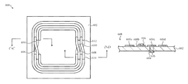
- FIG. 6A depicts a top view of one layer of a multi-layer implementation of an electrically-balanced inductor 600 of a wireless power system, such as described herein.
- crossovers can be formed between different turns of the electrically-balanced inductor 600 with a combination of vias and jumpers.
- the electrically-balanced inductor 600 can be formed onto a substrate 602 .
- the substrate 602 can be any suitable dielectric substrate.
- the substrate 602 is a circuit board layer, a polymer film, or a glass sheet.
- the substrate 602 can be flexible or rigid, and may be made from a single layer of material or multiple layers of material.
- the electrically-balanced inductor 600 can be formed or adhered onto different portions of the substrate 602 .
- the electrically-balanced inductor 600 includes four turn portions along a top portion and four turn portions along a bottom portion. These turn portions are coupled together with crossovers 604 , 606 , 608 , 610 , 612 , and 614 . Some of the crossovers are associated with a top surface of the substrate 602 , such as the crossovers 606 , 610 , and 614 whereas other crossovers are associated with a bottom surface of the substrate 602 , such as the crossovers 604 , 608 , and 612 .
- the crossovers on the bottom surface of the substrate can be coupled to portions of the electrically-balanced inductor 600 formed on the top surface of the substrate with through-substrate vias.
- portions of the electrically-balanced inductor 600 on the top of the substrate are identified, respectively, as the turns 600 a , 600 b , 600 c , and 600 d .
- the crossover 606 is electrically coupled to the turn 600 b .
- the crossover 604 on the underside of the substrate 602 , is connected to the turn 600 c through the via 616 .
- portions of the electrically-balanced inductor 600 on the top of the substrate are identified, respectively, as the turns 600 e , 600 f , 600 g , and 600 a .
- the crossover 610 is electrically coupled to the turn 600 f and the crossover 614 is electrically coupled to the turn 600 a .
- the crossover 612 and the crossover 612 , on the underside of the substrate 602 are respectively connected to the turn 600 e and the turn 600 g the vias 618 , 620 .
- the electrically-balanced inductor 600 can be formed with multiple layers, such as shown in FIG. 6D .
- the electrically-balanced inductor 600 can be formed by electrically connecting independent substrates to one another.
- the electrically-balanced inductor 600 can be formed with multiple layers of turns. In some examples, crossovers can be included between different turns of different layers.
- the electrically-balanced inductor 600 can be formed by laminating different layers or sheets of material together. For example, as shown in FIG. 6E , three layers can be laminated together to for the electrically-balanced inductor 600 .
- a first crossover layer 626 can be positioned over a turn layer 628 which in turn is positioned over a second crossover layer 630 .
- the first crossover layer 626 and the second crossover layer 630 each include one or more conductive traces that are configured to align with conductive traces (e.g., turns) on the turn layer 628 .
- the electrically conductive traces of the first crossover layer 626 , the second crossover layer 630 and the turn layer 628 can be formed into the substrate 602 or onto a layer of the substrate 60 in any suitable manner.
- electrically conductive traces associated with one or more of the first crossover layer 626 , the second crossover layer 630 and the turn layer 628 can be formed into the substrate 602 can be formed by physical vapor deposition, electroplating, electroless plating, etching, or any other suitable method.
- electrically conductive traces associated with one or more of the first crossover layer 626 , the second crossover layer 630 and the turn layer 628 can be formed into the substrate 602 can be formed by adhering metal to the substrate or a layer of the substrate.
- the various electrically conductive metals selected for the first crossover layer 626 , the second crossover layer 630 and the turn layer 628 can be formed into the substrate 602 may be the same or they may be different.
- Example metals that may be suitable include copper, gold, silver, and so on.
- FIG. 6A-6E the various alternatives thereof and variations thereto is presented, generally, for purposes of explanation, and to facilitate an understanding of various example methods of manufacturing and/or constructing an electrically-balanced inductor such as described herein. It will be apparent to one skilled in the art that some of the specific details presented herein may not be required in order to practice a particular described embodiment, or an equivalent thereof.
- a substrate can be made from a thin polymer. Electrically conductive traces can be formed onto the polymer using a suitable method.
- the substrate can be made from glass, sapphire, plastic, or another inorganic material.
- a substrate can be a multi-layer circuit board.
- an electrically-balanced inductor can be formed in another manner.
- an electrically-balanced inductor can be formed by wrapping wire onto a mandrel in a manner that introduces crossovers. For example, while wrapping the mandrel, separators or shims can be inserted that correspond to turns that have yet to be formed.
- an electrically-balanced inductor can be formed as a part of an array of electrically-balanced inductors on the same substrate.
- the substrate can be a single-layer substrate, a stack of independent substrates, or a multi-layer substrate.
- an electrically-balanced inductor can be formed by molding.
- adjacent turns can be connected by mold material channels that are removed in a subsequent operation (e.g., by etching).
- an electrically-balanced inductor can be formed by additive manufacturing methods including, but not limited to, electroforming and/or electroplating, three and dimensional plating.
- insulators can be inserted or formed between different turns of the electrically-balanced inductor.
- an electrically-balanced inductor can be formed by subtractive manufacturing methods including, but not limited to, laser etching and/or ablation, mechanical scribing and/or cutting, water or particle jet abrasion and/or cutting, and so on.
- an electrically-balanced inductor can be formed by severing a conventional inductor (e.g., having spiraling turns) and reconnecting severed portions of the inductor with crossovers.
- FIG. 7 is a simplified flow chart corresponding to a method of manufacturing an inductor.
- the method 700 can be used to form an electrically-balanced inductor such as described herein.
- method 700 can be used to form an electrically-balanced inductor suitable for use in either a receiver device or a transmitter device of a wireless power system, such as described above with reference to FIGS. 1A-2B .
- method 700 includes at operation 702 in which turn traces are formed on one or more layers of a multi-layer circuit board.
- one or more electrical connections e.g., crossovers
- the electrical connections can be made by vias, jumpers, separate circuit layers, solder bridges, or any other suitable method.
- leads of the electrically-balanced inductor is coupled to transmit circuitry.
- FIG. 8 is a simplified flow chart corresponding to another method of manufacturing an inductor.
- method 800 can be used to form an electrically-balanced inductor such as described herein.
- the method 800 can be used to form an electrically-balanced inductor suitable for use in either a receiver device or a transmitter device of a wireless power system, such as described above with reference to FIGS. 1A-2B .
- method 800 includes operation 802 in which a coil mold is prepared to receive mold material.
- the coil mold includes a mold cavity that defines a complete electrically-balanced inductor.
- the coil mold includes a mold cavity that defines only a portion of an electrically-balanced inductor, such as a radial section of an electrically-balanced inductor.
- coil material can be introduced into the mold.
- Suitable coil mold materials include, but are not limited to: copper, gold, evaporative pattern casting material, and so on.
- the molded part is removed from the mold.
- FIG. 9 is a simplified flow chart corresponding to another method of manufacturing an inductor.
- Method 900 includes operation 902 in which a coil is formed without crossovers using a suitable and/or conventional technique.
- portions of the coil can be cut in order to form crossovers between radially-adjacent sections of turns of the coil.
- FIG. 10 is a simplified flow chart corresponding to another method of manufacturing an inductor, such as described herein.
- Method 1000 includes operation 1002 in which a first turn layer is deposited onto a substrate.
- an insulator layer is deposited over the turn layer.
- the insulator layer may optionally include one or more apertures or windows through which an electrical connection can be made.
- a second turn layer can be deposited over the insulator layer.
- an electrical connection can be made between the first turn layer and the second turn layer.
Landscapes
- Engineering & Computer Science (AREA)
- Power Engineering (AREA)
- Computer Networks & Wireless Communication (AREA)
- Manufacturing & Machinery (AREA)
- Charge And Discharge Circuits For Batteries Or The Like (AREA)
- Near-Field Transmission Systems (AREA)
- Coils Or Transformers For Communication (AREA)
- Filters And Equalizers (AREA)
Abstract
Description
Claims (17)
Priority Applications (3)
| Application Number | Priority Date | Filing Date | Title |
|---|---|---|---|
| US15/474,569 US10594160B2 (en) | 2017-01-11 | 2017-03-30 | Noise mitigation in wireless power systems |
| PCT/US2018/012795 WO2018132333A1 (en) | 2017-01-11 | 2018-01-08 | Noise mitigation in wireless power systems |
| SG11201803901XA SG11201803901XA (en) | 2017-01-11 | 2018-01-08 | Noise mitigation in wireless power systems |
Applications Claiming Priority (2)
| Application Number | Priority Date | Filing Date | Title |
|---|---|---|---|
| US201762445202P | 2017-01-11 | 2017-01-11 | |
| US15/474,569 US10594160B2 (en) | 2017-01-11 | 2017-03-30 | Noise mitigation in wireless power systems |
Publications (2)
| Publication Number | Publication Date |
|---|---|
| US20180198318A1 US20180198318A1 (en) | 2018-07-12 |
| US10594160B2 true US10594160B2 (en) | 2020-03-17 |
Family
ID=62783502
Family Applications (1)
| Application Number | Title | Priority Date | Filing Date |
|---|---|---|---|
| US15/474,569 Expired - Fee Related US10594160B2 (en) | 2017-01-11 | 2017-03-30 | Noise mitigation in wireless power systems |
Country Status (3)
| Country | Link |
|---|---|
| US (1) | US10594160B2 (en) |
| SG (1) | SG11201803901XA (en) |
| WO (1) | WO2018132333A1 (en) |
Cited By (2)
| Publication number | Priority date | Publication date | Assignee | Title |
|---|---|---|---|---|
| US20200403449A1 (en) * | 2015-12-22 | 2020-12-24 | Intel Corporation | Uniform wireless charging device |
| US11979030B2 (en) | 2016-08-26 | 2024-05-07 | Apple Inc. | Shared power converter for a wireless transmitter device |
Families Citing this family (7)
| Publication number | Priority date | Publication date | Assignee | Title |
|---|---|---|---|---|
| US10790699B2 (en) | 2015-09-24 | 2020-09-29 | Apple Inc. | Configurable wireless transmitter device |
| US10477741B1 (en) | 2015-09-29 | 2019-11-12 | Apple Inc. | Communication enabled EMF shield enclosures |
| US10651685B1 (en) | 2015-09-30 | 2020-05-12 | Apple Inc. | Selective activation of a wireless transmitter device |
| US10594160B2 (en) | 2017-01-11 | 2020-03-17 | Apple Inc. | Noise mitigation in wireless power systems |
| JP7069836B2 (en) * | 2018-03-02 | 2022-05-18 | トヨタ自動車株式会社 | Coil unit |
| DE102018215972A1 (en) * | 2018-09-19 | 2020-03-19 | Fraunhofer-Gesellschaft zur Förderung der angewandten Forschung e.V. | Method and tool for producing a coil and coil produced therewith |
| GB201915064D0 (en) * | 2019-10-17 | 2019-12-04 | Univ Liverpool | Apparatus for and method of wireless power transfer |
Citations (135)
| Publication number | Priority date | Publication date | Assignee | Title |
|---|---|---|---|---|
| US3502809A (en) | 1966-02-04 | 1970-03-24 | Technical Material Corp | Method and apparatus for phase- or frequency-modulating signals at high power levels by means of saturable magnetic cores |
| JPS5510608B2 (en) | 1972-10-03 | 1980-03-18 | ||
| US4785136A (en) | 1986-11-10 | 1988-11-15 | Mollet John R | Electromagnetic interference shielding cover |
| US4871220A (en) | 1988-06-15 | 1989-10-03 | Litton Systems, Inc. | Short wavelength pass filter having a metal mesh on a semiconducting substrate |
| US5373102A (en) | 1993-08-19 | 1994-12-13 | The United States Of America As Represented By The Secretary Of The Army | Optically transmissive Faraday cage |
| US5384575A (en) | 1988-09-26 | 1995-01-24 | Hughes Aircraft Company | Bandpass frequency selective surface |
| US5496966A (en) | 1991-06-12 | 1996-03-05 | Bellsouth Corporation | Method for controlling indoor electromagnetic signal propagation |
| US5545844A (en) | 1993-08-03 | 1996-08-13 | The Zippertubing Company | Quick access electrical shielding chamber |
| US5563614A (en) | 1989-12-19 | 1996-10-08 | Her Majesty In Right Of Canada, As Represented By The Minister Of Communications | Low noise dual polarization electromagnetic power reception and conversion system |
| US5760584A (en) | 1996-08-16 | 1998-06-02 | General Electric Company | Shield for MR system RF coil provided with multiple capacitive channels for RF current flow |
| US6144512A (en) | 1984-02-21 | 2000-11-07 | Lockheed Martin Corporation | Dynamic filter structures |
| US6269247B1 (en) | 1997-11-27 | 2001-07-31 | Alcatel | Method of spatial location of a mobile station in a cell of a communication network and corresponding base station, mobile station and signaling packet |
| US6449181B1 (en) | 1999-10-01 | 2002-09-10 | Robert Bosch Gmbh | Inverter for conversion of electrical energy |
| US20020137473A1 (en) | 2001-03-12 | 2002-09-26 | Jenkins Deborah L. | Radiation shield for cellular telephones |
| US6492587B1 (en) | 1999-06-21 | 2002-12-10 | Nec Corporation | EMI shield filter and display apparatus having EMI shield filter |
| US20040021376A1 (en) | 2001-05-15 | 2004-02-05 | Klaus Beulich | Converter for electrical machines |
| US6724950B2 (en) | 2000-03-31 | 2004-04-20 | Board Of Regents, The University Of Texas System | Electro-optically tunable filter with mesh structure to filter optical signal |
| US6768051B2 (en) | 2000-03-06 | 2004-07-27 | Marconi Optical Components Limited | Screens for RF magnetic flux |
| US6864419B2 (en) | 2003-06-26 | 2005-03-08 | Inductotherm Corp. | Electromagnetic shield for an induction heating coil |
| US6927574B2 (en) | 2000-03-06 | 2005-08-09 | Koninklijke Phillips Electronics N.V. | Magnetic resonance apparatus including an rf magnetic flux guiding structure for improving the signal-to-noise ratio |
| US7035087B2 (en) | 2003-08-17 | 2006-04-25 | Micro-Star Int'l Co., Ltd. | Electronic apparatus with a housing for seeing inside |
| US7068140B2 (en) | 2003-11-18 | 2006-06-27 | Via Technologies, Inc. | Coplanar transformer with a capacitor |
| US7170363B2 (en) | 2000-03-06 | 2007-01-30 | Marconi Uk Intellectual Property Ltd. | Guides for r.f. magnetic flux |
| WO2008032746A1 (en) | 2006-09-12 | 2008-03-20 | The University Of Tokyo | Power supply sheet and electrically connecting circuit |
| US20080067914A1 (en) | 2006-09-18 | 2008-03-20 | Lg Electronics Inc. | Plasma display apparatus and manufacturing method of electromagnetic wave interference blocking filter therefor |
| CN101202277A (en) | 2007-10-26 | 2008-06-18 | 威盛电子股份有限公司 | Symmetric inductance element |
| KR20080081480A (en) | 2007-03-05 | 2008-09-10 | 엘에스전선 주식회사 | Wireless charger having multiple coil pad and battery charging set having the same |
| US20080303479A1 (en) * | 2005-07-29 | 2008-12-11 | Dong-Young Park | Contact-Less Chargeable Battery and Charging Device, Battery Charging Set, and Charging Control Method Thereof |
| US7466077B2 (en) | 2004-01-17 | 2008-12-16 | Samsung Corning Co., Ltd. | Filter assembly, method of manufacturing the same, and plasma display panel using the same |
| US20090052721A1 (en) | 2005-12-21 | 2009-02-26 | Koninklijke Philips Electronics, N.V. | Combined inductive charging coil and audio speaker for use in a personal care appliance |
| WO2009081126A1 (en) | 2007-12-21 | 2009-07-02 | Amway (Europe) Limited | Circuitry for inductive power transfer |
| US7639206B2 (en) | 2008-05-05 | 2009-12-29 | University Of Central Florida Research Foundation, Inc. | Low-profile frequency selective surface based device and methods of making the same |
| US20100015918A1 (en) | 2008-07-18 | 2010-01-21 | Ferro Solutions, Inc. | Wireless transfer of information using magneto-electric devices |
| US7679205B1 (en) | 2004-02-20 | 2010-03-16 | Phillip Burns | Method and apparatus for converting energy to electricity |
| US7705591B2 (en) | 2007-06-29 | 2010-04-27 | The Boeing Company | Radio frequency sensor systems, electromagnetic sensor arrays, and methods of manufacture |
| US7732038B2 (en) | 2004-07-12 | 2010-06-08 | Dai Nippon Printing Co., Ltd. | Electromagnetic wave shielding filter |
| US7737370B2 (en) | 2006-07-31 | 2010-06-15 | Hitachi Cable, Ltd. | Electromagnetic shielding filter |
| EP2211438A1 (en) | 2009-01-27 | 2010-07-28 | Panasonic Electric Works Co., Ltd. | Contactless power transmission system |
| US7791311B2 (en) | 2005-10-24 | 2010-09-07 | Samsung Electronics Co., Ltd. | Apparatus and method of wirelessly sharing power by inductive method |
| EP2256895A1 (en) | 2009-05-28 | 2010-12-01 | Koninklijke Philips Electronics N.V. | Inductive power system and method |
| US20110050164A1 (en) | 2008-05-07 | 2011-03-03 | Afshin Partovi | System and methods for inductive charging, and improvements and uses thereof |
| US7906936B2 (en) | 2007-10-09 | 2011-03-15 | Powermat Ltd. | Rechargeable inductive charger |
| US20110101788A1 (en) * | 2008-09-12 | 2011-05-05 | University Of Pittsburgh - Of The Commonwealth System Of Higher Education | Wireless Energy Transfer System |
| US7948781B2 (en) | 2007-06-01 | 2011-05-24 | Sanyo Electric Co., Ltd. | Contactless power receiving unit and electronic device employing the same |
| US7948208B2 (en) | 2006-06-01 | 2011-05-24 | Mojo Mobility, Inc. | Power source, charging system, and inductive receiver for mobile devices |
| US7952322B2 (en) | 2006-01-31 | 2011-05-31 | Mojo Mobility, Inc. | Inductive power source and charging system |
| US20110164471A1 (en) * | 2010-01-05 | 2011-07-07 | Access Business Group International Llc | Integrated wireless power system |
| US20110169770A1 (en) | 2010-01-13 | 2011-07-14 | Alps Electric Co., Ltd. | Antenna embedded input device and electronic device having the device |
| US8050063B2 (en) | 2007-05-31 | 2011-11-01 | General Electric Company | Systems and methods for controlling a converter for powering a load |
| US8101931B2 (en) | 2010-04-05 | 2012-01-24 | Miltec Corporation | RF screen assembly for microwave powered UV lamps |
| US8115448B2 (en) | 2007-06-01 | 2012-02-14 | Michael Sasha John | Systems and methods for wireless power |
| US8169185B2 (en) | 2006-01-31 | 2012-05-01 | Mojo Mobility, Inc. | System and method for inductive charging of portable devices |
| US20120104997A1 (en) | 2010-11-01 | 2012-05-03 | Qualcomm Incorporated | Wireless charging device |
| US20120139358A1 (en) | 2010-12-01 | 2012-06-07 | Triune Ip Llc | Multiple Coil Data Transmission System |
| US20120198364A1 (en) | 2011-01-31 | 2012-08-02 | Sap Ag | User interface style guide compliance reporting |
| US8262244B2 (en) | 2009-05-12 | 2012-09-11 | Kimball International, Inc. | Furniture with wireless power |
| US8338990B2 (en) | 2008-03-13 | 2012-12-25 | Access Business Group International Llc | Inductive power supply system with multiple coil primary |
| US20130043734A1 (en) | 2011-08-16 | 2013-02-21 | Qualcomm Incorporated | Wireless power receiver with multiple receiver coils |
| US8436317B1 (en) | 2011-11-09 | 2013-05-07 | Hermes-Microvision, Inc. | Wien filter |
| US8531153B2 (en) | 2008-07-09 | 2013-09-10 | Access Business Group International Llc | Wireless charging system |
| US20130271069A1 (en) | 2012-03-21 | 2013-10-17 | Mojo Mobility, Inc. | Systems and methods for wireless power transfer |
| US20130285604A1 (en) | 2011-01-18 | 2013-10-31 | Mojo Mobility, Inc. | Systems and methods for wireless power transfer |
| US20130285605A1 (en) | 2011-01-18 | 2013-10-31 | Mojo Mobility, Inc. | Systems and methods for wireless power transfer |
| US20130300204A1 (en) | 2011-01-18 | 2013-11-14 | Mojo Mobility, Inc. | Systems and methods for wireless power transfer |
| US8587154B2 (en) | 2007-08-28 | 2013-11-19 | Access Business Group International Llc | Inductive power supply |
| US20140035383A1 (en) | 2012-08-03 | 2014-02-06 | Mediatek Singapore Pte. Ltd. | Dual-mode wireless power receiver |
| US8723053B2 (en) | 2011-03-09 | 2014-05-13 | Select Fabricators, Inc. | Electromagnetically shielded enclosure with operable interfaces |
| US20140132210A1 (en) | 2012-03-21 | 2014-05-15 | Mojo Mobility, Inc. | System and method for charging or powering devices, such as robots, electric vehicles, or other mobile devices or equipment |
| US8729734B2 (en) | 2007-11-16 | 2014-05-20 | Qualcomm Incorporated | Wireless power bridge |
| JP5510608B2 (en) | 2011-03-11 | 2014-06-04 | トヨタ自動車株式会社 | Coil unit, vehicle, external power supply device, and vehicle charging system |
| US8760113B2 (en) | 2009-02-24 | 2014-06-24 | Qualcomm Incorporated | Wireless power charging timing and charging control |
| US20140191568A1 (en) | 2013-01-04 | 2014-07-10 | Mojo Mobility, Inc. | System and method for powering or charging multiple receivers wirelessly with a power transmitter |
| US8779745B2 (en) | 2010-03-01 | 2014-07-15 | National Semiconductor Corporation | Three-quarter bridge power converters for wireless power transfer applications and other applications |
| US8810196B2 (en) | 2008-09-05 | 2014-08-19 | Koninklijke Philips N.V. | Inductive charger and charging method |
| US8836276B2 (en) | 2011-03-07 | 2014-09-16 | Eldon Technology Limited | Charging batteries for electronic devices by talking |
| US8838022B2 (en) | 2010-04-13 | 2014-09-16 | Radeum, Inc. | System and method for securely pairing a wireless device using wireless communication |
| US20140306654A1 (en) | 2013-04-12 | 2014-10-16 | Mojo Mobility, Inc. | System and method for powering or charging receivers or devices having small surface areas or volumes |
| US8890470B2 (en) | 2010-06-11 | 2014-11-18 | Mojo Mobility, Inc. | System for wireless power transfer that supports interoperability, and multi-pole magnets for use therewith |
| US20140354279A1 (en) | 2013-05-29 | 2014-12-04 | Children's Hospital Medical Center | Faraday Cage For MR Imaging With Accessory Equipment |
| US8928284B2 (en) | 2009-09-10 | 2015-01-06 | Qualcomm Incorporated | Variable wireless power transmission |
| US8947892B1 (en) | 2010-08-16 | 2015-02-03 | The Boeing Company | Electronic device protection |
| CN104347259A (en) | 2013-07-23 | 2015-02-11 | 佳邦科技股份有限公司 | Improved thin power inductor manufacturing process |
| US20150043424A1 (en) | 2013-08-06 | 2015-02-12 | The Boeing Company | Wired ethernet adaptor for portable electronic devices |
| US9001031B2 (en) | 2012-07-30 | 2015-04-07 | Qualcomm Mems Technologies, Inc. | Complex passive design with special via implementation |
| US9025143B2 (en) | 2010-11-12 | 2015-05-05 | Industry-Academic Cooperation Foundation Yonsei University | Device for preventing intensity reduction of optical signal, optical emission spectrometer, optical instrument, and mass spectrometer including the same |
| US9041152B2 (en) | 2013-03-14 | 2015-05-26 | Taiwan Semiconductor Manufacturing Company, Ltd. | Inductor with magnetic material |
| US9065423B2 (en) | 2008-09-27 | 2015-06-23 | Witricity Corporation | Wireless energy distribution system |
| US9071062B2 (en) | 2009-02-26 | 2015-06-30 | The University Of British Columbia | Systems and methods for dipole enhanced inductive power transfer |
| US9106083B2 (en) | 2011-01-18 | 2015-08-11 | Mojo Mobility, Inc. | Systems and method for positioning freedom, and support of different voltages, protocols, and power levels in a wireless power system |
| US9118203B2 (en) | 2011-11-15 | 2015-08-25 | Qualcomm Incorporated | Systems and methods for induction charging with a closed magnetic loop |
| US9153998B2 (en) | 2013-12-02 | 2015-10-06 | Qualcomm Incorporated | Wireless power orthogonal polarization antenna array |
| US20150288193A1 (en) | 2014-04-04 | 2015-10-08 | Apple Inc. | Inductive Power Transfer Using Acoustic or Haptic Devices |
| US9161484B2 (en) | 2010-09-26 | 2015-10-13 | Access Business Group International Llc | Selectively controllable electromagnetic shielding |
| US20150303706A1 (en) * | 2014-04-16 | 2015-10-22 | Witricity Corporation | Wireless energy transfer for mobile device applications |
| US9171555B2 (en) | 2010-09-10 | 2015-10-27 | Seagate Technology Llc | Magnetic flux barrier |
| US9177716B2 (en) | 2011-08-25 | 2015-11-03 | Panasonic Intellectual Property Management Co., Ltd. | Method for detecting metal foreign object in contactless power supply system, contactless power supply device, power reception device, and contactless power supply system |
| US20150318710A1 (en) | 2012-12-13 | 2015-11-05 | Lg Innotek Co., Ltd. | Wireless power receiver and method of controlling the same |
| US20150326028A1 (en) * | 2011-09-21 | 2015-11-12 | Pioneer Corporation | Wireless power transmitting apparatus, wireless power receiving apparatus, and wireless power feeding system |
| US20150333562A1 (en) | 2014-05-16 | 2015-11-19 | Samsung Electro-Mechanics Co., Ltd. | Wireless charging transmitter and wireless charging system using the same |
| US20150333530A1 (en) | 2014-05-19 | 2015-11-19 | Apple Inc. | Operating a Wireless Power Transfer System at Multiple Frequencies |
| US9209627B2 (en) | 2010-08-25 | 2015-12-08 | Access Business Group International Llc | Wireless power supply system and multi-layer shim assembly |
| US9217323B2 (en) | 2012-09-24 | 2015-12-22 | Schlumberger Technology Corporation | Mechanical caliper system for a logging while drilling (LWD) borehole caliper |
| US20160036261A1 (en) | 2014-07-29 | 2016-02-04 | Cambridge Silicon Radio Limited | Wireless Charger With Resonator |
| US20160064137A1 (en) | 2014-09-02 | 2016-03-03 | Apple Inc. | Capacitively balanced inductive charging coil |
| US9281759B2 (en) | 2012-01-27 | 2016-03-08 | Lg Electronics Inc. | Power converting apparatus and photovoltaic module |
| US9300147B2 (en) | 2011-06-29 | 2016-03-29 | Lg Electronics Inc. | Method for avoiding signal collision in wireless power transfer |
| US20160172894A1 (en) | 2014-12-16 | 2016-06-16 | Samsung Electronics Co., Ltd. | Wireless charger and wireless power receiver |
| US20160181853A1 (en) | 2014-12-23 | 2016-06-23 | Intel Corporation | Low emission coil topology for wireless charging |
| US20160196943A1 (en) | 2013-08-06 | 2016-07-07 | The Regents Of The University Of Michigan | RECONFIGURABLE DEVICE FOR TERAHERTZ (THz) AND INFRARED (IR) FILTERING AND MODULATION |
| US20160284465A1 (en) | 2015-03-29 | 2016-09-29 | Sanjaya Maniktala | Electromagnetic Interference Shield for Wireless Power Transfer |
| US9497894B1 (en) | 2015-07-22 | 2016-11-15 | John Gordon Ramsey | Low impedance radiofrequency shielded window |
| US20160372948A1 (en) | 2015-06-18 | 2016-12-22 | David Kristian Kvols | RFI/EMI Shielding Enclosure Containing Wireless Charging Element for Personal Electronic Devices Security |
| US9548158B2 (en) | 2014-12-02 | 2017-01-17 | Globalfoundries Inc. | 3D multipath inductor |
| US20170047162A1 (en) * | 2014-11-27 | 2017-02-16 | Brusa Elektronik Ag | Transmitter coils for contactless energy transmission systems with coupling enhancement and stray field reduction |
| US9577460B2 (en) | 2013-10-31 | 2017-02-21 | Samsung Electro-Mechanics Co., Ltd. | Wireless charging device and control method thereof |
| US20170092409A1 (en) | 2015-09-30 | 2017-03-30 | Apple Inc. | Preferentially Magnetically Oriented Ferrites for Improved Power Transfer |
| US20170093199A1 (en) | 2015-09-24 | 2017-03-30 | Apple Inc. | Configurable Wireless Transmitter Device |
| US9620983B2 (en) | 2013-10-01 | 2017-04-11 | Intel Corporation | Ultrasonic universal wireless charging |
| US9643507B2 (en) | 2013-10-03 | 2017-05-09 | The Boeing Company | Recharging an aircraft battery |
| US9711272B2 (en) | 2015-07-09 | 2017-07-18 | Te Connectivity Corporation | Printed circuit for wireless power transfer |
| US9726518B2 (en) | 2012-07-13 | 2017-08-08 | Qualcomm Incorporated | Systems, methods, and apparatus for detection of metal objects in a predetermined space |
| US9748326B2 (en) | 2014-10-06 | 2017-08-29 | Realtek Semiconductor Corporation | Structure of integrated inductor |
| US20170279305A1 (en) | 2014-10-27 | 2017-09-28 | Koninklijke Philips N.V. | Wireless inductive power transfer |
| US9831686B2 (en) | 2013-03-05 | 2017-11-28 | Panasonic Intellectual Property Management Co., Ltd. | Wireless power transmission device |
| US20170353046A1 (en) * | 2016-06-02 | 2017-12-07 | Qualcomm Incorporated | Modular and assemblable wireless charging system and device |
| US9862282B2 (en) | 2013-02-11 | 2018-01-09 | Sew-Eurodrive Gmbh & Co. Kg | Device having a winding configuration and system, especially charging station, for the non-contact transmission of energy to an electric-powered vehicle, having a winding configuration |
| US9893553B2 (en) | 2013-12-24 | 2018-02-13 | Pavan Pudipeddi | Method and system for simultaneously wirelessly charging portable rechargeable devices based on wireless inductive power transfer with seamless free positioning capability |
| US20180048503A1 (en) * | 2015-03-06 | 2018-02-15 | Lg Electronics Inc. | Data transmission method and apparatus in wireless communication system |
| US20180062430A1 (en) * | 2015-03-23 | 2018-03-01 | Mitsubishi Electric Corporation | Bidirectional non-contact power supply device and bidirectional non-contact power supply system |
| US20180062442A1 (en) | 2016-08-26 | 2018-03-01 | Apple Inc. | Shared Power Converter for a Wireless Transmitter Device |
| US20180198318A1 (en) | 2017-01-11 | 2018-07-12 | Apple Inc. | Noise Mitigation in Wireless Power Systems |
| US20180226822A1 (en) | 2016-05-18 | 2018-08-09 | International Business Machines Corporation | Wireless charging surface |
| US10141785B2 (en) | 2014-01-03 | 2018-11-27 | Wilus Institute Of Standards And Technology Inc. | Wireless power transmission apparatus and wireless power transmission method |
| US20190058348A1 (en) | 2017-08-15 | 2019-02-21 | Toyota Motor Engineering & Manufacturing North America, Inc. | Configurable grid charging coil with active switch and sensing system |
| US10477741B1 (en) | 2015-09-29 | 2019-11-12 | Apple Inc. | Communication enabled EMF shield enclosures |
-
2017
- 2017-03-30 US US15/474,569 patent/US10594160B2/en not_active Expired - Fee Related
-
2018
- 2018-01-08 WO PCT/US2018/012795 patent/WO2018132333A1/en active Application Filing
- 2018-01-08 SG SG11201803901XA patent/SG11201803901XA/en unknown
Patent Citations (158)
| Publication number | Priority date | Publication date | Assignee | Title |
|---|---|---|---|---|
| US3502809A (en) | 1966-02-04 | 1970-03-24 | Technical Material Corp | Method and apparatus for phase- or frequency-modulating signals at high power levels by means of saturable magnetic cores |
| JPS5510608B2 (en) | 1972-10-03 | 1980-03-18 | ||
| US6144512A (en) | 1984-02-21 | 2000-11-07 | Lockheed Martin Corporation | Dynamic filter structures |
| US4785136A (en) | 1986-11-10 | 1988-11-15 | Mollet John R | Electromagnetic interference shielding cover |
| US4871220A (en) | 1988-06-15 | 1989-10-03 | Litton Systems, Inc. | Short wavelength pass filter having a metal mesh on a semiconducting substrate |
| US5384575A (en) | 1988-09-26 | 1995-01-24 | Hughes Aircraft Company | Bandpass frequency selective surface |
| US5563614A (en) | 1989-12-19 | 1996-10-08 | Her Majesty In Right Of Canada, As Represented By The Minister Of Communications | Low noise dual polarization electromagnetic power reception and conversion system |
| US5496966A (en) | 1991-06-12 | 1996-03-05 | Bellsouth Corporation | Method for controlling indoor electromagnetic signal propagation |
| US5545844A (en) | 1993-08-03 | 1996-08-13 | The Zippertubing Company | Quick access electrical shielding chamber |
| US5373102A (en) | 1993-08-19 | 1994-12-13 | The United States Of America As Represented By The Secretary Of The Army | Optically transmissive Faraday cage |
| US5760584A (en) | 1996-08-16 | 1998-06-02 | General Electric Company | Shield for MR system RF coil provided with multiple capacitive channels for RF current flow |
| US6269247B1 (en) | 1997-11-27 | 2001-07-31 | Alcatel | Method of spatial location of a mobile station in a cell of a communication network and corresponding base station, mobile station and signaling packet |
| US6492587B1 (en) | 1999-06-21 | 2002-12-10 | Nec Corporation | EMI shield filter and display apparatus having EMI shield filter |
| US6449181B1 (en) | 1999-10-01 | 2002-09-10 | Robert Bosch Gmbh | Inverter for conversion of electrical energy |
| US7170363B2 (en) | 2000-03-06 | 2007-01-30 | Marconi Uk Intellectual Property Ltd. | Guides for r.f. magnetic flux |
| US6768051B2 (en) | 2000-03-06 | 2004-07-27 | Marconi Optical Components Limited | Screens for RF magnetic flux |
| US6927574B2 (en) | 2000-03-06 | 2005-08-09 | Koninklijke Phillips Electronics N.V. | Magnetic resonance apparatus including an rf magnetic flux guiding structure for improving the signal-to-noise ratio |
| US6724950B2 (en) | 2000-03-31 | 2004-04-20 | Board Of Regents, The University Of Texas System | Electro-optically tunable filter with mesh structure to filter optical signal |
| US20020137473A1 (en) | 2001-03-12 | 2002-09-26 | Jenkins Deborah L. | Radiation shield for cellular telephones |
| US20040021376A1 (en) | 2001-05-15 | 2004-02-05 | Klaus Beulich | Converter for electrical machines |
| US6864419B2 (en) | 2003-06-26 | 2005-03-08 | Inductotherm Corp. | Electromagnetic shield for an induction heating coil |
| US7035087B2 (en) | 2003-08-17 | 2006-04-25 | Micro-Star Int'l Co., Ltd. | Electronic apparatus with a housing for seeing inside |
| US7068140B2 (en) | 2003-11-18 | 2006-06-27 | Via Technologies, Inc. | Coplanar transformer with a capacitor |
| US7466077B2 (en) | 2004-01-17 | 2008-12-16 | Samsung Corning Co., Ltd. | Filter assembly, method of manufacturing the same, and plasma display panel using the same |
| US7679205B1 (en) | 2004-02-20 | 2010-03-16 | Phillip Burns | Method and apparatus for converting energy to electricity |
| US7732038B2 (en) | 2004-07-12 | 2010-06-08 | Dai Nippon Printing Co., Ltd. | Electromagnetic wave shielding filter |
| US20080303479A1 (en) * | 2005-07-29 | 2008-12-11 | Dong-Young Park | Contact-Less Chargeable Battery and Charging Device, Battery Charging Set, and Charging Control Method Thereof |
| US7791311B2 (en) | 2005-10-24 | 2010-09-07 | Samsung Electronics Co., Ltd. | Apparatus and method of wirelessly sharing power by inductive method |
| US20090052721A1 (en) | 2005-12-21 | 2009-02-26 | Koninklijke Philips Electronics, N.V. | Combined inductive charging coil and audio speaker for use in a personal care appliance |
| US20110221385A1 (en) | 2006-01-31 | 2011-09-15 | Mojo Mobility, Inc. | Inductive power source and charging system |
| US8947047B2 (en) | 2006-01-31 | 2015-02-03 | Mojo Mobility, Inc. | Efficiency and flexibility in inductive charging |
| US20130099563A1 (en) | 2006-01-31 | 2013-04-25 | Mojo Mobility, Inc. | Distributed charging of mobile devices |
| US8169185B2 (en) | 2006-01-31 | 2012-05-01 | Mojo Mobility, Inc. | System and method for inductive charging of portable devices |
| US7952322B2 (en) | 2006-01-31 | 2011-05-31 | Mojo Mobility, Inc. | Inductive power source and charging system |
| US8629654B2 (en) | 2006-01-31 | 2014-01-14 | Mojo Mobility, Inc. | System and method for inductive charging of portable devices |
| US9276437B2 (en) | 2006-01-31 | 2016-03-01 | Mojo Mobility, Inc. | System and method that provides efficiency and flexiblity in inductive charging |
| US8629652B2 (en) | 2006-06-01 | 2014-01-14 | Mojo Mobility, Inc. | Power source, charging system, and inductive receiver for mobile devices |
| US7948208B2 (en) | 2006-06-01 | 2011-05-24 | Mojo Mobility, Inc. | Power source, charging system, and inductive receiver for mobile devices |
| US20140103873A1 (en) | 2006-06-01 | 2014-04-17 | Mojo Mobility, Inc. | Power source, charging system, and inductive receiver for mobile devices |
| US7737370B2 (en) | 2006-07-31 | 2010-06-15 | Hitachi Cable, Ltd. | Electromagnetic shielding filter |
| WO2008032746A1 (en) | 2006-09-12 | 2008-03-20 | The University Of Tokyo | Power supply sheet and electrically connecting circuit |
| US20080067914A1 (en) | 2006-09-18 | 2008-03-20 | Lg Electronics Inc. | Plasma display apparatus and manufacturing method of electromagnetic wave interference blocking filter therefor |
| KR20080081480A (en) | 2007-03-05 | 2008-09-10 | 엘에스전선 주식회사 | Wireless charger having multiple coil pad and battery charging set having the same |
| US8050063B2 (en) | 2007-05-31 | 2011-11-01 | General Electric Company | Systems and methods for controlling a converter for powering a load |
| US7948781B2 (en) | 2007-06-01 | 2011-05-24 | Sanyo Electric Co., Ltd. | Contactless power receiving unit and electronic device employing the same |
| US8115448B2 (en) | 2007-06-01 | 2012-02-14 | Michael Sasha John | Systems and methods for wireless power |
| US7705591B2 (en) | 2007-06-29 | 2010-04-27 | The Boeing Company | Radio frequency sensor systems, electromagnetic sensor arrays, and methods of manufacture |
| US8587154B2 (en) | 2007-08-28 | 2013-11-19 | Access Business Group International Llc | Inductive power supply |
| US7906936B2 (en) | 2007-10-09 | 2011-03-15 | Powermat Ltd. | Rechargeable inductive charger |
| US8193769B2 (en) | 2007-10-18 | 2012-06-05 | Powermat Technologies, Ltd | Inductively chargeable audio devices |
| CN101202277A (en) | 2007-10-26 | 2008-06-18 | 威盛电子股份有限公司 | Symmetric inductance element |
| US8729734B2 (en) | 2007-11-16 | 2014-05-20 | Qualcomm Incorporated | Wireless power bridge |
| WO2009081126A1 (en) | 2007-12-21 | 2009-07-02 | Amway (Europe) Limited | Circuitry for inductive power transfer |
| US8338990B2 (en) | 2008-03-13 | 2012-12-25 | Access Business Group International Llc | Inductive power supply system with multiple coil primary |
| US7639206B2 (en) | 2008-05-05 | 2009-12-29 | University Of Central Florida Research Foundation, Inc. | Low-profile frequency selective surface based device and methods of making the same |
| US20110050164A1 (en) | 2008-05-07 | 2011-03-03 | Afshin Partovi | System and methods for inductive charging, and improvements and uses thereof |
| US20130093388A1 (en) | 2008-05-07 | 2013-04-18 | Mojo Mobility, Inc. | Inductive charging including use of after-market accessories |
| US20130260677A1 (en) | 2008-05-07 | 2013-10-03 | Mojo Mobility, Inc. | Contextually aware charging of mobile devices |
| US8531153B2 (en) | 2008-07-09 | 2013-09-10 | Access Business Group International Llc | Wireless charging system |
| US20100015918A1 (en) | 2008-07-18 | 2010-01-21 | Ferro Solutions, Inc. | Wireless transfer of information using magneto-electric devices |
| US8810196B2 (en) | 2008-09-05 | 2014-08-19 | Koninklijke Philips N.V. | Inductive charger and charging method |
| US20110101788A1 (en) * | 2008-09-12 | 2011-05-05 | University Of Pittsburgh - Of The Commonwealth System Of Higher Education | Wireless Energy Transfer System |
| US8421274B2 (en) | 2008-09-12 | 2013-04-16 | University Of Pittsburgh-Of The Commonwealth System Of Higher Education | Wireless energy transfer system |
| US9065423B2 (en) | 2008-09-27 | 2015-06-23 | Witricity Corporation | Wireless energy distribution system |
| EP2211438A1 (en) | 2009-01-27 | 2010-07-28 | Panasonic Electric Works Co., Ltd. | Contactless power transmission system |
| US8760113B2 (en) | 2009-02-24 | 2014-06-24 | Qualcomm Incorporated | Wireless power charging timing and charging control |
| US9071062B2 (en) | 2009-02-26 | 2015-06-30 | The University Of British Columbia | Systems and methods for dipole enhanced inductive power transfer |
| US8262244B2 (en) | 2009-05-12 | 2012-09-11 | Kimball International, Inc. | Furniture with wireless power |
| EP2256895A1 (en) | 2009-05-28 | 2010-12-01 | Koninklijke Philips Electronics N.V. | Inductive power system and method |
| US8928284B2 (en) | 2009-09-10 | 2015-01-06 | Qualcomm Incorporated | Variable wireless power transmission |
| US20110164471A1 (en) * | 2010-01-05 | 2011-07-07 | Access Business Group International Llc | Integrated wireless power system |
| US20110169770A1 (en) | 2010-01-13 | 2011-07-14 | Alps Electric Co., Ltd. | Antenna embedded input device and electronic device having the device |
| US8779745B2 (en) | 2010-03-01 | 2014-07-15 | National Semiconductor Corporation | Three-quarter bridge power converters for wireless power transfer applications and other applications |
| US8101931B2 (en) | 2010-04-05 | 2012-01-24 | Miltec Corporation | RF screen assembly for microwave powered UV lamps |
| US8838022B2 (en) | 2010-04-13 | 2014-09-16 | Radeum, Inc. | System and method for securely pairing a wireless device using wireless communication |
| US8896264B2 (en) | 2010-06-11 | 2014-11-25 | Mojo Mobility, Inc. | Inductive charging with support for multiple charging protocols |
| US20150130412A1 (en) | 2010-06-11 | 2015-05-14 | Mojo Mobility, Inc. | Intelligent initiation of inductive charging process |
| US8890470B2 (en) | 2010-06-11 | 2014-11-18 | Mojo Mobility, Inc. | System for wireless power transfer that supports interoperability, and multi-pole magnets for use therewith |
| US8901881B2 (en) | 2010-06-11 | 2014-12-02 | Mojo Mobility, Inc. | Intelligent initiation of inductive charging process |
| US8947892B1 (en) | 2010-08-16 | 2015-02-03 | The Boeing Company | Electronic device protection |
| US9209627B2 (en) | 2010-08-25 | 2015-12-08 | Access Business Group International Llc | Wireless power supply system and multi-layer shim assembly |
| US9171555B2 (en) | 2010-09-10 | 2015-10-27 | Seagate Technology Llc | Magnetic flux barrier |
| US9161484B2 (en) | 2010-09-26 | 2015-10-13 | Access Business Group International Llc | Selectively controllable electromagnetic shielding |
| US20120104997A1 (en) | 2010-11-01 | 2012-05-03 | Qualcomm Incorporated | Wireless charging device |
| US9025143B2 (en) | 2010-11-12 | 2015-05-05 | Industry-Academic Cooperation Foundation Yonsei University | Device for preventing intensity reduction of optical signal, optical emission spectrometer, optical instrument, and mass spectrometer including the same |
| US20120139358A1 (en) | 2010-12-01 | 2012-06-07 | Triune Ip Llc | Multiple Coil Data Transmission System |
| US9178369B2 (en) | 2011-01-18 | 2015-11-03 | Mojo Mobility, Inc. | Systems and methods for providing positioning freedom, and support of different voltages, protocols, and power levels in a wireless power system |
| US20130285604A1 (en) | 2011-01-18 | 2013-10-31 | Mojo Mobility, Inc. | Systems and methods for wireless power transfer |
| US9112364B2 (en) | 2011-01-18 | 2015-08-18 | Mojo Mobility, Inc. | Multi-dimensional inductive charger and applications thereof |
| US9356659B2 (en) | 2011-01-18 | 2016-05-31 | Mojo Mobility, Inc. | Chargers and methods for wireless power transfer |
| US20130300204A1 (en) | 2011-01-18 | 2013-11-14 | Mojo Mobility, Inc. | Systems and methods for wireless power transfer |
| US9112362B2 (en) | 2011-01-18 | 2015-08-18 | Mojo Mobility, Inc. | Methods for improved transfer efficiency in a multi-dimensional inductive charger |
| US9112363B2 (en) | 2011-01-18 | 2015-08-18 | Mojo Mobility, Inc. | Intelligent charging of multiple electric or electronic devices with a multi-dimensional inductive charger |
| US9106083B2 (en) | 2011-01-18 | 2015-08-11 | Mojo Mobility, Inc. | Systems and method for positioning freedom, and support of different voltages, protocols, and power levels in a wireless power system |
| US20130285605A1 (en) | 2011-01-18 | 2013-10-31 | Mojo Mobility, Inc. | Systems and methods for wireless power transfer |
| US20120198364A1 (en) | 2011-01-31 | 2012-08-02 | Sap Ag | User interface style guide compliance reporting |
| US8836276B2 (en) | 2011-03-07 | 2014-09-16 | Eldon Technology Limited | Charging batteries for electronic devices by talking |
| US8723053B2 (en) | 2011-03-09 | 2014-05-13 | Select Fabricators, Inc. | Electromagnetically shielded enclosure with operable interfaces |
| JP5510608B2 (en) | 2011-03-11 | 2014-06-04 | トヨタ自動車株式会社 | Coil unit, vehicle, external power supply device, and vehicle charging system |
| US9124126B2 (en) | 2011-03-11 | 2015-09-01 | Toyota Jidosha Kabushiki Kaisha | Coil unit, power transmission device, external power feeding apparatus, and vehicle charging system |
| US9300147B2 (en) | 2011-06-29 | 2016-03-29 | Lg Electronics Inc. | Method for avoiding signal collision in wireless power transfer |
| US20130043734A1 (en) | 2011-08-16 | 2013-02-21 | Qualcomm Incorporated | Wireless power receiver with multiple receiver coils |
| US9177716B2 (en) | 2011-08-25 | 2015-11-03 | Panasonic Intellectual Property Management Co., Ltd. | Method for detecting metal foreign object in contactless power supply system, contactless power supply device, power reception device, and contactless power supply system |
| US20150326028A1 (en) * | 2011-09-21 | 2015-11-12 | Pioneer Corporation | Wireless power transmitting apparatus, wireless power receiving apparatus, and wireless power feeding system |
| US8436317B1 (en) | 2011-11-09 | 2013-05-07 | Hermes-Microvision, Inc. | Wien filter |
| US9118203B2 (en) | 2011-11-15 | 2015-08-25 | Qualcomm Incorporated | Systems and methods for induction charging with a closed magnetic loop |
| US9281759B2 (en) | 2012-01-27 | 2016-03-08 | Lg Electronics Inc. | Power converting apparatus and photovoltaic module |
| US20140132210A1 (en) | 2012-03-21 | 2014-05-15 | Mojo Mobility, Inc. | System and method for charging or powering devices, such as robots, electric vehicles, or other mobile devices or equipment |
| US20130271069A1 (en) | 2012-03-21 | 2013-10-17 | Mojo Mobility, Inc. | Systems and methods for wireless power transfer |
| US9726518B2 (en) | 2012-07-13 | 2017-08-08 | Qualcomm Incorporated | Systems, methods, and apparatus for detection of metal objects in a predetermined space |
| US9001031B2 (en) | 2012-07-30 | 2015-04-07 | Qualcomm Mems Technologies, Inc. | Complex passive design with special via implementation |
| US20140035383A1 (en) | 2012-08-03 | 2014-02-06 | Mediatek Singapore Pte. Ltd. | Dual-mode wireless power receiver |
| US9217323B2 (en) | 2012-09-24 | 2015-12-22 | Schlumberger Technology Corporation | Mechanical caliper system for a logging while drilling (LWD) borehole caliper |
| US20150318710A1 (en) | 2012-12-13 | 2015-11-05 | Lg Innotek Co., Ltd. | Wireless power receiver and method of controlling the same |
| US20140191568A1 (en) | 2013-01-04 | 2014-07-10 | Mojo Mobility, Inc. | System and method for powering or charging multiple receivers wirelessly with a power transmitter |
| US9862282B2 (en) | 2013-02-11 | 2018-01-09 | Sew-Eurodrive Gmbh & Co. Kg | Device having a winding configuration and system, especially charging station, for the non-contact transmission of energy to an electric-powered vehicle, having a winding configuration |
| US9831686B2 (en) | 2013-03-05 | 2017-11-28 | Panasonic Intellectual Property Management Co., Ltd. | Wireless power transmission device |
| US9041152B2 (en) | 2013-03-14 | 2015-05-26 | Taiwan Semiconductor Manufacturing Company, Ltd. | Inductor with magnetic material |
| US20140306654A1 (en) | 2013-04-12 | 2014-10-16 | Mojo Mobility, Inc. | System and method for powering or charging receivers or devices having small surface areas or volumes |
| US20140354279A1 (en) | 2013-05-29 | 2014-12-04 | Children's Hospital Medical Center | Faraday Cage For MR Imaging With Accessory Equipment |
| CN104347259A (en) | 2013-07-23 | 2015-02-11 | 佳邦科技股份有限公司 | Improved thin power inductor manufacturing process |
| US20160196943A1 (en) | 2013-08-06 | 2016-07-07 | The Regents Of The University Of Michigan | RECONFIGURABLE DEVICE FOR TERAHERTZ (THz) AND INFRARED (IR) FILTERING AND MODULATION |
| US20150043424A1 (en) | 2013-08-06 | 2015-02-12 | The Boeing Company | Wired ethernet adaptor for portable electronic devices |
| US9620983B2 (en) | 2013-10-01 | 2017-04-11 | Intel Corporation | Ultrasonic universal wireless charging |
| US9643507B2 (en) | 2013-10-03 | 2017-05-09 | The Boeing Company | Recharging an aircraft battery |
| US9577460B2 (en) | 2013-10-31 | 2017-02-21 | Samsung Electro-Mechanics Co., Ltd. | Wireless charging device and control method thereof |
| US9153998B2 (en) | 2013-12-02 | 2015-10-06 | Qualcomm Incorporated | Wireless power orthogonal polarization antenna array |
| US9893553B2 (en) | 2013-12-24 | 2018-02-13 | Pavan Pudipeddi | Method and system for simultaneously wirelessly charging portable rechargeable devices based on wireless inductive power transfer with seamless free positioning capability |
| US10141785B2 (en) | 2014-01-03 | 2018-11-27 | Wilus Institute Of Standards And Technology Inc. | Wireless power transmission apparatus and wireless power transmission method |
| US20150288193A1 (en) | 2014-04-04 | 2015-10-08 | Apple Inc. | Inductive Power Transfer Using Acoustic or Haptic Devices |
| US20150303707A1 (en) | 2014-04-16 | 2015-10-22 | Witricity Corporation | Wireless energy transfer for mobile device applications |
| US20150303706A1 (en) * | 2014-04-16 | 2015-10-22 | Witricity Corporation | Wireless energy transfer for mobile device applications |
| US9735628B2 (en) | 2014-04-16 | 2017-08-15 | Witricity Corporation | Wireless energy transfer for mobile device applications |
| US9917479B2 (en) | 2014-04-16 | 2018-03-13 | Witricity Corporation | Wireless energy transfer for mobile device applications |
| US20150333562A1 (en) | 2014-05-16 | 2015-11-19 | Samsung Electro-Mechanics Co., Ltd. | Wireless charging transmitter and wireless charging system using the same |
| US20150333530A1 (en) | 2014-05-19 | 2015-11-19 | Apple Inc. | Operating a Wireless Power Transfer System at Multiple Frequencies |
| US20160036261A1 (en) | 2014-07-29 | 2016-02-04 | Cambridge Silicon Radio Limited | Wireless Charger With Resonator |
| US20160064137A1 (en) | 2014-09-02 | 2016-03-03 | Apple Inc. | Capacitively balanced inductive charging coil |
| US9748326B2 (en) | 2014-10-06 | 2017-08-29 | Realtek Semiconductor Corporation | Structure of integrated inductor |
| US20170279305A1 (en) | 2014-10-27 | 2017-09-28 | Koninklijke Philips N.V. | Wireless inductive power transfer |
| US20170047162A1 (en) * | 2014-11-27 | 2017-02-16 | Brusa Elektronik Ag | Transmitter coils for contactless energy transmission systems with coupling enhancement and stray field reduction |
| US9548158B2 (en) | 2014-12-02 | 2017-01-17 | Globalfoundries Inc. | 3D multipath inductor |
| US20160172894A1 (en) | 2014-12-16 | 2016-06-16 | Samsung Electronics Co., Ltd. | Wireless charger and wireless power receiver |
| US20160181853A1 (en) | 2014-12-23 | 2016-06-23 | Intel Corporation | Low emission coil topology for wireless charging |
| US20180048503A1 (en) * | 2015-03-06 | 2018-02-15 | Lg Electronics Inc. | Data transmission method and apparatus in wireless communication system |
| US20180062430A1 (en) * | 2015-03-23 | 2018-03-01 | Mitsubishi Electric Corporation | Bidirectional non-contact power supply device and bidirectional non-contact power supply system |
| US20160284465A1 (en) | 2015-03-29 | 2016-09-29 | Sanjaya Maniktala | Electromagnetic Interference Shield for Wireless Power Transfer |
| US20160372948A1 (en) | 2015-06-18 | 2016-12-22 | David Kristian Kvols | RFI/EMI Shielding Enclosure Containing Wireless Charging Element for Personal Electronic Devices Security |
| US9711272B2 (en) | 2015-07-09 | 2017-07-18 | Te Connectivity Corporation | Printed circuit for wireless power transfer |
| US9497894B1 (en) | 2015-07-22 | 2016-11-15 | John Gordon Ramsey | Low impedance radiofrequency shielded window |
| US20170093199A1 (en) | 2015-09-24 | 2017-03-30 | Apple Inc. | Configurable Wireless Transmitter Device |
| US10477741B1 (en) | 2015-09-29 | 2019-11-12 | Apple Inc. | Communication enabled EMF shield enclosures |
| US20170092409A1 (en) | 2015-09-30 | 2017-03-30 | Apple Inc. | Preferentially Magnetically Oriented Ferrites for Improved Power Transfer |
| US20180226822A1 (en) | 2016-05-18 | 2018-08-09 | International Business Machines Corporation | Wireless charging surface |
| US20170353046A1 (en) * | 2016-06-02 | 2017-12-07 | Qualcomm Incorporated | Modular and assemblable wireless charging system and device |
| US20180062442A1 (en) | 2016-08-26 | 2018-03-01 | Apple Inc. | Shared Power Converter for a Wireless Transmitter Device |
| US20180198318A1 (en) | 2017-01-11 | 2018-07-12 | Apple Inc. | Noise Mitigation in Wireless Power Systems |
| US20190058348A1 (en) | 2017-08-15 | 2019-02-21 | Toyota Motor Engineering & Manufacturing North America, Inc. | Configurable grid charging coil with active switch and sensing system |
Non-Patent Citations (2)
| Title |
|---|
| Invitation to Pay Additional Fees and Search Report dated Mar. 23, 2018; PCT/US2018/012795; 11 pages. |
| U.S. Appl. No. 10/044,232, filed Aug. 2018, Crosby et al. |
Cited By (2)
| Publication number | Priority date | Publication date | Assignee | Title |
|---|---|---|---|---|
| US20200403449A1 (en) * | 2015-12-22 | 2020-12-24 | Intel Corporation | Uniform wireless charging device |
| US11979030B2 (en) | 2016-08-26 | 2024-05-07 | Apple Inc. | Shared power converter for a wireless transmitter device |
Also Published As
| Publication number | Publication date |
|---|---|
| US20180198318A1 (en) | 2018-07-12 |
| WO2018132333A4 (en) | 2018-08-23 |
| WO2018132333A1 (en) | 2018-07-19 |
| SG11201803901XA (en) | 2018-08-30 |
Similar Documents
| Publication | Publication Date | Title |
|---|---|---|
| US10594160B2 (en) | Noise mitigation in wireless power systems | |
| US11538622B2 (en) | High current, low equivalent series resistance printed circuit board coil for power transfer application | |
| US10523063B2 (en) | Common mode noise compensation in wireless power systems | |
| TWI522026B (en) | Substrate having electronic component embedded therein and method of manufacturing the same | |
| CN102170605B (en) | Micro-electro-mechanical microphone and be integrated with the MEMS microphone chip of filter | |
| CN107408442B (en) | Common mode noise filter | |
| TWI571047B (en) | Lc composite component | |
| JPWO2015147132A1 (en) | Antenna device and communication device | |
| US9659709B2 (en) | Common mode filter and manufacturing method thereof | |
| JP2013105756A (en) | Electronic component to be incorporated into wiring substrate and part built-in type substrate | |
| US9577598B2 (en) | Thin film type common mode filter | |
| US10848120B2 (en) | Multilayer LC filter | |
| EP3340748B1 (en) | Multilayer substrate | |
| JP2015087888A (en) | Non-contact communication module and card reader | |
| KR20140028452A (en) | Coil component | |
| CN107452460B (en) | Electronic component | |
| KR101922870B1 (en) | Common mode filter | |
| KR101530066B1 (en) | Common mode filter and manufacturing method thereof | |
| JP2015130607A (en) | Communication device | |
| CN210042406U (en) | Embedded substrate and electronic equipment | |
| WO2021148585A1 (en) | Position-free, multiple output capacitive power transfer system | |
| WO2019015525A1 (en) | Hearing aid compatible mobile terminal structure | |
| US9236847B2 (en) | Common mode filter | |
| TWI508361B (en) | Common mode filter | |
| CN108174504A (en) | A kind of PCB circuit board |
Legal Events
| Date | Code | Title | Description |
|---|---|---|---|
| AS | Assignment |
Owner name: APPLE INC., CALIFORNIA Free format text: ASSIGNMENT OF ASSIGNORS INTEREST;ASSIGNORS:JAIN, KARAN S.;DATTA, SUPRATIK;VENUGOPAL, NANDITA;AND OTHERS;SIGNING DATES FROM 20170322 TO 20170323;REEL/FRAME:041801/0330 |
|
| STPP | Information on status: patent application and granting procedure in general |
Free format text: NON FINAL ACTION MAILED |
|
| STPP | Information on status: patent application and granting procedure in general |
Free format text: RESPONSE TO NON-FINAL OFFICE ACTION ENTERED AND FORWARDED TO EXAMINER |
|
| STPP | Information on status: patent application and granting procedure in general |
Free format text: NOTICE OF ALLOWANCE MAILED -- APPLICATION RECEIVED IN OFFICE OF PUBLICATIONS |
|
| STPP | Information on status: patent application and granting procedure in general |
Free format text: AWAITING TC RESP., ISSUE FEE NOT PAID |
|
| STPP | Information on status: patent application and granting procedure in general |
Free format text: NOTICE OF ALLOWANCE MAILED -- APPLICATION RECEIVED IN OFFICE OF PUBLICATIONS |
|
| STPP | Information on status: patent application and granting procedure in general |
Free format text: PUBLICATIONS -- ISSUE FEE PAYMENT VERIFIED |
|
| STPP | Information on status: patent application and granting procedure in general |
Free format text: DOCKETED NEW CASE - READY FOR EXAMINATION |
|
| STPP | Information on status: patent application and granting procedure in general |
Free format text: NOTICE OF ALLOWANCE MAILED -- APPLICATION RECEIVED IN OFFICE OF PUBLICATIONS |
|
| STPP | Information on status: patent application and granting procedure in general |
Free format text: AWAITING TC RESP., ISSUE FEE NOT PAID |
|
| STPP | Information on status: patent application and granting procedure in general |
Free format text: PUBLICATIONS -- ISSUE FEE PAYMENT VERIFIED |
|
| STCF | Information on status: patent grant |
Free format text: PATENTED CASE |
|
| FEPP | Fee payment procedure |
Free format text: MAINTENANCE FEE REMINDER MAILED (ORIGINAL EVENT CODE: REM.); ENTITY STATUS OF PATENT OWNER: LARGE ENTITY |
|
| LAPS | Lapse for failure to pay maintenance fees |
Free format text: PATENT EXPIRED FOR FAILURE TO PAY MAINTENANCE FEES (ORIGINAL EVENT CODE: EXP.); ENTITY STATUS OF PATENT OWNER: LARGE ENTITY |
|
| STCH | Information on status: patent discontinuation |
Free format text: PATENT EXPIRED DUE TO NONPAYMENT OF MAINTENANCE FEES UNDER 37 CFR 1.362 |