US10566949B2 - Micromachined ultrasound transducer using multiple piezoelectric materials - Google Patents
Micromachined ultrasound transducer using multiple piezoelectric materials Download PDFInfo
- Publication number
- US10566949B2 US10566949B2 US15/342,719 US201615342719A US10566949B2 US 10566949 B2 US10566949 B2 US 10566949B2 US 201615342719 A US201615342719 A US 201615342719A US 10566949 B2 US10566949 B2 US 10566949B2
- Authority
- US
- United States
- Prior art keywords
- piezoelectric
- transducer
- electrode
- layer
- electrodes
- Prior art date
- Legal status (The legal status is an assumption and is not a legal conclusion. Google has not performed a legal analysis and makes no representation as to the accuracy of the status listed.)
- Active, expires
Links
- 239000000463 material Substances 0.000 title claims abstract description 62
- 238000002604 ultrasonography Methods 0.000 title description 14
- 239000000758 substrate Substances 0.000 claims description 20
- 229910052451 lead zirconate titanate Inorganic materials 0.000 claims description 14
- XLOMVQKBTHCTTD-UHFFFAOYSA-N Zinc monoxide Chemical compound [Zn]=O XLOMVQKBTHCTTD-UHFFFAOYSA-N 0.000 claims description 6
- PIGFYZPCRLYGLF-UHFFFAOYSA-N Aluminum nitride Chemical compound [Al]#N PIGFYZPCRLYGLF-UHFFFAOYSA-N 0.000 claims description 5
- HFGPZNIAWCZYJU-UHFFFAOYSA-N lead zirconate titanate Chemical compound [O-2].[O-2].[O-2].[O-2].[O-2].[Ti+4].[Zr+4].[Pb+2] HFGPZNIAWCZYJU-UHFFFAOYSA-N 0.000 claims description 5
- BITYAPCSNKJESK-UHFFFAOYSA-N potassiosodium Chemical compound [Na].[K] BITYAPCSNKJESK-UHFFFAOYSA-N 0.000 claims description 5
- 229910052751 metal Inorganic materials 0.000 description 7
- 239000002184 metal Substances 0.000 description 7
- VYPSYNLAJGMNEJ-UHFFFAOYSA-N Silicium dioxide Chemical compound O=[Si]=O VYPSYNLAJGMNEJ-UHFFFAOYSA-N 0.000 description 6
- 238000000034 method Methods 0.000 description 6
- 230000035945 sensitivity Effects 0.000 description 6
- PMHQVHHXPFUNSP-UHFFFAOYSA-M copper(1+);methylsulfanylmethane;bromide Chemical compound Br[Cu].CSC PMHQVHHXPFUNSP-UHFFFAOYSA-M 0.000 description 5
- 230000009977 dual effect Effects 0.000 description 5
- 230000000694 effects Effects 0.000 description 5
- 229910052581 Si3N4 Inorganic materials 0.000 description 3
- 239000000377 silicon dioxide Substances 0.000 description 3
- HQVNEWCFYHHQES-UHFFFAOYSA-N silicon nitride Chemical compound N12[Si]34N5[Si]62N3[Si]51N64 HQVNEWCFYHHQES-UHFFFAOYSA-N 0.000 description 3
- FYYHWMGAXLPEAU-UHFFFAOYSA-N Magnesium Chemical compound [Mg] FYYHWMGAXLPEAU-UHFFFAOYSA-N 0.000 description 2
- XUIMIQQOPSSXEZ-UHFFFAOYSA-N Silicon Chemical compound [Si] XUIMIQQOPSSXEZ-UHFFFAOYSA-N 0.000 description 2
- 238000005452 bending Methods 0.000 description 2
- 238000000151 deposition Methods 0.000 description 2
- 238000013461 design Methods 0.000 description 2
- 239000012530 fluid Substances 0.000 description 2
- 239000011777 magnesium Substances 0.000 description 2
- 229910052749 magnesium Inorganic materials 0.000 description 2
- 239000012528 membrane Substances 0.000 description 2
- 229910021420 polycrystalline silicon Inorganic materials 0.000 description 2
- 229910052710 silicon Inorganic materials 0.000 description 2
- 239000010703 silicon Substances 0.000 description 2
- 235000012239 silicon dioxide Nutrition 0.000 description 2
- 239000011734 sodium Substances 0.000 description 2
- 229910052782 aluminium Inorganic materials 0.000 description 1
- 238000013459 approach Methods 0.000 description 1
- 238000003491 array Methods 0.000 description 1
- 238000004891 communication Methods 0.000 description 1
- 239000002131 composite material Substances 0.000 description 1
- 239000004020 conductor Substances 0.000 description 1
- 230000003247 decreasing effect Effects 0.000 description 1
- 230000008021 deposition Effects 0.000 description 1
- 238000011161 development Methods 0.000 description 1
- 238000002059 diagnostic imaging Methods 0.000 description 1
- 239000002305 electric material Substances 0.000 description 1
- 238000005516 engineering process Methods 0.000 description 1
- 238000005530 etching Methods 0.000 description 1
- 230000002349 favourable effect Effects 0.000 description 1
- 150000002500 ions Chemical class 0.000 description 1
- 238000001459 lithography Methods 0.000 description 1
- 229910052750 molybdenum Inorganic materials 0.000 description 1
- 229910021421 monocrystalline silicon Inorganic materials 0.000 description 1
- 238000009659 non-destructive testing Methods 0.000 description 1
- 238000000059 patterning Methods 0.000 description 1
- 229910052697 platinum Inorganic materials 0.000 description 1
- 229920005591 polysilicon Polymers 0.000 description 1
- 238000012545 processing Methods 0.000 description 1
- 238000011160 research Methods 0.000 description 1
- 239000004065 semiconductor Substances 0.000 description 1
- 239000010409 thin film Substances 0.000 description 1
- 239000011787 zinc oxide Substances 0.000 description 1
Images


Classifications
-
- H—ELECTRICITY
- H03—ELECTRONIC CIRCUITRY
- H03H—IMPEDANCE NETWORKS, e.g. RESONANT CIRCUITS; RESONATORS
- H03H9/00—Networks comprising electromechanical or electro-acoustic devices; Electromechanical resonators
- H03H9/15—Constructional features of resonators consisting of piezoelectric or electrostrictive material
- H03H9/17—Constructional features of resonators consisting of piezoelectric or electrostrictive material having a single resonator
- H03H9/171—Constructional features of resonators consisting of piezoelectric or electrostrictive material having a single resonator implemented with thin-film techniques, i.e. of the film bulk acoustic resonator [FBAR] type
- H03H9/172—Means for mounting on a substrate, i.e. means constituting the material interface confining the waves to a volume
- H03H9/174—Membranes
-
- B—PERFORMING OPERATIONS; TRANSPORTING
- B06—GENERATING OR TRANSMITTING MECHANICAL VIBRATIONS IN GENERAL
- B06B—METHODS OR APPARATUS FOR GENERATING OR TRANSMITTING MECHANICAL VIBRATIONS OF INFRASONIC, SONIC, OR ULTRASONIC FREQUENCY, e.g. FOR PERFORMING MECHANICAL WORK IN GENERAL
- B06B1/00—Methods or apparatus for generating mechanical vibrations of infrasonic, sonic, or ultrasonic frequency
- B06B1/02—Methods or apparatus for generating mechanical vibrations of infrasonic, sonic, or ultrasonic frequency making use of electrical energy
- B06B1/06—Methods or apparatus for generating mechanical vibrations of infrasonic, sonic, or ultrasonic frequency making use of electrical energy operating with piezoelectric effect or with electrostriction
- B06B1/0603—Methods or apparatus for generating mechanical vibrations of infrasonic, sonic, or ultrasonic frequency making use of electrical energy operating with piezoelectric effect or with electrostriction using a piezoelectric bender, e.g. bimorph
-
- H—ELECTRICITY
- H03—ELECTRONIC CIRCUITRY
- H03H—IMPEDANCE NETWORKS, e.g. RESONANT CIRCUITS; RESONATORS
- H03H9/00—Networks comprising electromechanical or electro-acoustic devices; Electromechanical resonators
- H03H9/02—Details
- H03H9/02244—Details of microelectro-mechanical resonators
-
- H—ELECTRICITY
- H03—ELECTRONIC CIRCUITRY
- H03H—IMPEDANCE NETWORKS, e.g. RESONANT CIRCUITS; RESONATORS
- H03H9/00—Networks comprising electromechanical or electro-acoustic devices; Electromechanical resonators
- H03H9/15—Constructional features of resonators consisting of piezoelectric or electrostrictive material
- H03H9/17—Constructional features of resonators consisting of piezoelectric or electrostrictive material having a single resonator
- H03H9/178—Constructional features of resonators consisting of piezoelectric or electrostrictive material having a single resonator of a laminated structure of multiple piezoelectric layers with inner electrodes
-
- H—ELECTRICITY
- H04—ELECTRIC COMMUNICATION TECHNIQUE
- H04R—LOUDSPEAKERS, MICROPHONES, GRAMOPHONE PICK-UPS OR LIKE ACOUSTIC ELECTROMECHANICAL TRANSDUCERS; DEAF-AID SETS; PUBLIC ADDRESS SYSTEMS
- H04R17/00—Piezoelectric transducers; Electrostrictive transducers
-
- H—ELECTRICITY
- H10—SEMICONDUCTOR DEVICES; ELECTRIC SOLID-STATE DEVICES NOT OTHERWISE PROVIDED FOR
- H10N—ELECTRIC SOLID-STATE DEVICES NOT OTHERWISE PROVIDED FOR
- H10N30/00—Piezoelectric or electrostrictive devices
- H10N30/20—Piezoelectric or electrostrictive devices with electrical input and mechanical output, e.g. functioning as actuators or vibrators
- H10N30/204—Piezoelectric or electrostrictive devices with electrical input and mechanical output, e.g. functioning as actuators or vibrators using bending displacement, e.g. unimorph, bimorph or multimorph cantilever or membrane benders
- H10N30/2047—Membrane type
-
- H—ELECTRICITY
- H10—SEMICONDUCTOR DEVICES; ELECTRIC SOLID-STATE DEVICES NOT OTHERWISE PROVIDED FOR
- H10N—ELECTRIC SOLID-STATE DEVICES NOT OTHERWISE PROVIDED FOR
- H10N30/00—Piezoelectric or electrostrictive devices
- H10N30/80—Constructional details
- H10N30/85—Piezoelectric or electrostrictive active materials
- H10N30/853—Ceramic compositions
- H10N30/8542—Alkali metal based oxides, e.g. lithium, sodium or potassium niobates
-
- H—ELECTRICITY
- H10—SEMICONDUCTOR DEVICES; ELECTRIC SOLID-STATE DEVICES NOT OTHERWISE PROVIDED FOR
- H10N—ELECTRIC SOLID-STATE DEVICES NOT OTHERWISE PROVIDED FOR
- H10N30/00—Piezoelectric or electrostrictive devices
- H10N30/80—Constructional details
- H10N30/85—Piezoelectric or electrostrictive active materials
- H10N30/853—Ceramic compositions
- H10N30/8548—Lead based oxides
- H10N30/8554—Lead zirconium titanate based
-
- H—ELECTRICITY
- H03—ELECTRONIC CIRCUITRY
- H03H—IMPEDANCE NETWORKS, e.g. RESONANT CIRCUITS; RESONATORS
- H03H9/00—Networks comprising electromechanical or electro-acoustic devices; Electromechanical resonators
- H03H9/15—Constructional features of resonators consisting of piezoelectric or electrostrictive material
- H03H2009/155—Constructional features of resonators consisting of piezoelectric or electrostrictive material using MEMS techniques
Definitions
- the present disclosure is generally related to micromachined ultrasound transducers and more particularly optimizing the transmit and receive sensitivity of piezoelectric micromachined ultrasound transducers (PMUTs) through the use of two distinct piezoelectric materials.
- PMUTs piezoelectric micromachined ultrasound transducers
- a unimorph structure consists of a single active layer of piezoelectric material sandwiched between two electrodes coupled with a passive bending layer.
- a voltage is applied across the electrodes, which induces a transverse stress in the piezoelectric layer via the inverse piezoelectric effect, resulting in an out-of-plane deflection which transmits an ultrasonic pressure wave into a gas or fluid.
- the applied pressure results in out-of-plane bending and the generation of measurable charge via the direct piezoelectric effect.
- Bimorph structures utilize two piezoelectric layers between patterned electrodes and are typically driven differentially.
- the piezoelectric material constants (piezoelectric coefficients, dielectric constant, Young's modulus, etc.) of the chosen piezoelectric material are only optimized for a single mode of operation, i.e., transmitter or receiver.
- the inability to optimize the transducer's sensitivity for both transmitter and receiver modes results in significant reduction in the system performance for ultrasonic systems commonly used in medical imaging, ranging, non-destructive testing, ultrasonic data communication, and gesture recognition applications.
- An aspect of the present disclosure is to provide a transducer that is optimized for use both as an ultrasound transmitter and as an ultrasound receiver by using multiple piezoelectric materials.
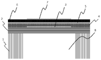
- FIG. 1 is a cross section of a circular embodiment of a dual material PMUT with a structural layer beneath the piezoelectric layers.
- FIG. 2 is a cross section showing PMUT deflection under applied voltage.
- FIG. 3A is an isometric view of an embodiment of a dual material PMUT with annular and circular electrodes.
- FIG. 3B is an electrical schematic illustrating an equivalent circuit to the PMUT shown in FIG. 3A .
- FIG. 4A is an isometric view of an additional circular embodiment of a dual material PMUT without the additional structural layer
- FIG. 4B is an equivalent circuit of the embodiment from FIG. 4A
- FIG. 4C is an isometric view of yet another embodiment in which there are four “electrodes” but only three “electrode layers”.
- FIGS. 5A-5F are a sequence of cross sections depicting an example of process flow for fabricating a PMUT in accordance with aspects of the present disclosure.
- FIG. 6 is an isometric view of an embodiment of an array of dual material PMUT devices.
- the present invention generally comprises a method to improve the performance of piezoelectric micromachined ultrasound transducers, of any shape, through the use of different piezoelectric materials for each mode of operation. More specifically, the invention provides a method to increase the transmit and receive sensitivity of an ultrasound transducer operating both as a transmitter and as a receiver. Aspects of the present disclosure apply to devices consisting of a single transducer or multiple transducers in an array.
- electrode layer is used to refer to a layer of conductive material, e.g., a metal, which may be patterned to form one or more “electrodes” (sometimes called contacts).
- a piezoelectric micromachined ultrasound transducer incorporates multiple distinct piezoelectric materials for operation as a transmitter and as a receiver.
- layers of piezoelectric materials with different properties such as, but not limited to: Young's modulus, piezoelectric coefficients, dielectric constant, and Poisson's ratio, transducer performance can be optimized to both transmit and receive sound.
- Young's modulus Young's modulus
- piezoelectric coefficients piezoelectric coefficients
- dielectric constant dielectric constant
- transducer performance can be optimized to both transmit and receive sound.
- the described method applies to individual transducers as well as 1 D and 2 D arrays of transducers fabricated on a common substrate.
- the transducer includes first and second piezoelectric layers made of corresponding different first and second piezoelectric materials and three or more electrodes, implemented in two or more conductive electrode layers.
- the first piezoelectric layer is sandwiched between a first pair of electrodes and the second piezoelectric layer is sandwiched between a second pair of electrodes.
- the first and second pairs of electrodes contain no more than one electrode that is common to both pairs.
- FIG. 1 shows a possible embodiment of the transducer, in cross section, according to the present invention.
- the PMUT consists of a suspended thin plate structure.
- the substrate 1 forms the supporting layer and is patterned to release the thin plate structure.
- the structural layer 2 provides additional plate thickness, thereby decreasing the sensitivity to residual stress in the thin film layers as well as enabling PMUTs to be fabricated with a range of possible operating frequencies, as required by different applications.
- the patterned receiver electrode 3 and the receiver piezoelectric layer 4 with material properties (piezoelectric coefficients, dielectric constant, Young's modulus, etc.) chosen for maximum receiver sensitivity, are deposited on top of the structural layer 2 .
- the ground electrode 5 and transmitter piezoelectric layer 6 are deposited and patterned along with the transmit electrode 7 .
- the electrodes 3 and 7 are shown as a circular electrode in the center of the suspended plate but other configurations, an outer ring for example, can be employed.
- the substrate 1 may act as an electrode if it is made of a semiconducting material, such as silicon.
- one of the metal layers that form electrodes 3 , 5 , 7 e.g., the layer forming the ground electrode 5 , may be omitted.
- An acoustic resonator tube 8 is incorporated into the design, e.g., by forming an opening through the substrate 1 to a back side of the structural layer 2 .
- the combination of the structural layer 2 , piezoelectric layers 4 , 6 and the metal layers 3 , 5 , and 7 is sometimes referred to as a diaphragm or membrane.
- transmitter mode a voltage is applied between the transmitter electrode 7 and the ground electrode 5 as shown in FIG. 2 . Due to the inverse piezoelectric effect, transverse stress is generated in the transmitter piezoelectric layer 6 , chosen for its desirable material properties in transmitter mode, which results in out of plane deflection. Reversing the voltage polarity, we obtain deflection in the opposite direction.
- the vibrating plate displaces gas or fluid, transmitting a pressure wave.
- an incoming pressure wave deflects the plate, generating a stress gradient in the receiver piezoelectric layer 4 , chosen to optimize receiver mode performance, which generates charge on the receiver electrode 3 and ground electrode 5 via the direct piezoelectric effect. The charge is measured electrically.
- one example of a dual material transducer is a combination aluminum nitride (AlN) and Lead Zirconate Titanate (PZT) transducer.
- PZT is chosen as the transmitter mode piezoelectric layer 6 due to its favorable transverse piezoelectric coefficient, e 31 , which is approximately 15 ⁇ larger than that of AlN. Since the output pressure is directly proportional to the piezoelectric coefficient, we can realize an increase in output pressure by using the PZT as the piezoelectric layer when transmitting. However, in receiver mode, the large dielectric constant of PZT and consequent increase in capacitance results in severely degraded receiver sensitivity relative to AlN.
- AlN is used as the receiver piezoelectric layer 4 .
- Alternative piezoelectric materials such as Potassium Sodium Niobate KNN (K x Na 1-x NbO 3 ) or PMN-PT (Lead Magnesium Niobate-Lead Titanate) may be used in place of PZT, while alternative materials such as ZnO may be used in place of AlN.
- the thickness of the structural layer 2 may be from 0.5 micron to 40 microns, and more specifically from 1 micron to 10 microns.
- the thickness of the piezoelectric layers 4 and 6 may be from 0.2 microns to 6 microns, and more specifically from 0.5 microns to 2.5 microns.
- the diameter of the transducer resonator tube 8 may be from 30 microns to 4000 microns, and specifically from 100 microns to 1500 microns, and more specifically from 400 microns to 1000 microns.
- the length of the acoustic resonator tube 8 may be from 10 microns to 4000 microns and more specifically from 150 microns to 450 microns.
- the operating frequency of the transducer may be from 1 kHz to 100 MHz, and specifically from 10 kHz to 1 MHz, and more specifically from 50 kHz to 500 kHz.
- the metal layer beneath the AlN piezoelectric layer may be Mo or Pt or Al, and may range in thickness from 100 nm to 500 nm.
- FIG. 3A illustrates an example of an implementation in which there are four “electrodes” but only two “electrode layers”.
- the transmitter piezoelectric material 19 is patterned to occupy an annular ring at the outer diameter of the transducer, with a transmitter electrode 22 patterned on top of the transmitter piezoelectric material 19 .
- the transmitter piezoelectric material 19 and a receiver piezoelectric material 20 are formed on a lower electrode layer 18 that is patterned into two bottom electrodes 18 A, 18 B.
- An upper electrode layer formed over the transmitter piezoelectric material 19 and receiver piezo electric material 20 is patterned to form a corresponding transmitter electrode 22 and receiver electrode 21 .
- the transmitter piezoelectric material 19 , transmitter electrode 22 , receiver piezoelectric material 20 and receiver electrode 21 are formed over an opening 23 in the substrate 16 .
- the opening frees structural layer 17 from the substrate 16 , allowing the membrane to vibrate.
- the length of the opening may be selected so that it acts as a resonator tube.
- the receiver piezoelectric material 20 is patterned into a circular region at the center of the transducer overlying the opening 23 with its accompanying receiver electrode 21 .
- the annular and central electrode configuration it is possible to differentially drive the transmitter and receiver electrodes to increase the output pressure per volt.
- FIG. 3B An equivalent circuit of the embodiment from FIG. 3A , illustrating the electrical connections to the first and second piezoelectric materials, is shown in FIG. 3B .
- the transmitter piezoelectric material 19 has two electrical contacts, top contact 22 and bottom contact 18 A.
- the receiver piezoelectric material 20 has two electrical contacts, top contact 21 and bottom contact 18 B.
- both of the bottom contacts 18 A, 18 B are made in the bottom electrode layer 18 , they can be electrically isolated, as shown in FIG. 3B , or they may be connected together.
- the structural layer may be omitted from the layer stack.
- FIG. 4A Piezoelectric layers 10 , 13 , and a ground electrode layer 12 are sandwiched between receiver electrode layer 11 and transmitter electrode layer 14 that overlie an opening 15 in substrate 9 .
- a voltage is applied between the top electrode layer 14 and the ground electrode layer 12 , thereby developing piezoelectric stress in the transmitter piezoelectric layer 13 .
- the receiver piezoelectric layer 10 acts as the passive structural layer, so that transverse piezoelectric stress in transmitter piezoelectric layer 13 results in an out-of-plane deflection of the structure.
- the transmitter piezoelectric layer 13 acts as the structural layer. In this case an incoming pressure wave deflects the plate, generating transverse stress in the receiver piezoelectric layer 10 , which generates a charge on the receiver electrode layer 11 via the direct piezoelectric effect. The charge is measured electrically.
- FIG. 4B An equivalent circuit of the embodiment from FIG. 4A , illustrating the electrical connections to the first and second piezoelectric materials, is shown in FIG. 4B .
- the transmitter piezoelectric layer 13 has two electrical contacts, a top contact formed from the transmitter electrode layer 14 and a bottom contact formed by the ground electrode layer 12 .
- the receiver piezoelectric layer 10 has two electrical contacts, a top contact formed from the receiver electrode layer 11 and bottom contact formed by the ground electrode layer 12 .
- FIG. 4C shows another embodiment in which these contacts are electrically isolated by patterning the ground electrode layer 12 .
- FIG. 4C illustrates an example in which there are four “electrodes” but only three “electrode layers”. Referring to FIG. 4C , piezoelectric layers 10 , 13 , and ground electrodes 12 A, 12 B formed from ground electrode layer 12 are sandwiched between receiver and transmitter electrodes 11 , 14 that overlie an opening 15 in substrate 9 .
- a voltage is applied between the annular ring top electrode 14 and the annular ring ground electrode 12 A, thereby developing piezoelectric stress in the transmitter piezoelectric layer 13 .
- the receiver piezoelectric layer 10 acts as the passive structural layer, so that transverse piezoelectric stress in transmitter layer 13 results in an out-of-plane deflection of the structure.
- the transmitter piezoelectric layer 13 acts as the structural layer. In this case an incoming pressure wave deflects the plate, generating transverse stress in the receiver piezoelectric layer 10 , which develops charge on the central circular receiver electrode 11 and the central circular ground electrode 12 B.
- FIGS. 5A-5F An example process flow is outlined in FIGS. 5A-5F .
- the process starts with the deposition of a structural layer 52 on a substrate 51 , as depicted in FIG. 5A .
- the structural layer 52 may be single crystal silicon, polysilicon, silicon nitride or silicon dioxide.
- a metal receiver electrode 53 is then patterned using lithography and etching, as shown in FIG. 5B .
- a receiver piezoelectric layer 54 , metal electrode 55 , and transmitter piezoelectric layers 56 are deposited and the transmitter electrode 57 is patterned on top as shown in FIG. 5C to FIG. 5D .
- Vias 58 are etched to expose the interconnect to the individual electrodes, as shown in FIG. 5E .
- the plate structure is released and an acoustic resonator tube 59 formed, e.g., by a deep reactive ion etch (DRIE).
- DRIE deep reactive ion etch
- FIG. 6 depicts an example of an array 60 containing multiple transducers 61 formed on a common substrate 62 .
- a transducer may include more than two piezoelectric layers and more than three electrodes. Therefore, it will be appreciated that the scope of the present invention fully encompasses other embodiments which may become obvious to those skilled in the art.
Abstract
Description
-
- 1. A piezoelectric micromachined ultrasound transducer with a diaphragm of any shape incorporating distinct piezoelectric materials for transmitter and receiver operation.
- 2. The piezoelectric micromachined ultrasound transducer recited in any preceding embodiment, wherein the transducer is an element of an array of transducers; and wherein the array comprises a plurality of transducers on a substrate.
- 3. The piezoelectric micromachined ultrasound transducer recited in any preceding embodiment, wherein the transducer diaphragm is square, rectangular, hexagonal, circular, or elliptical in shape.
- 4. The piezoelectric micromachined ultrasound transducer recited in any preceding embodiment, wherein any of the piezoelectric materials used are Aluminum Nitride (AlN), Zinc Oxide (ZnO), Potassium Sodium Niobate KNN (KxNa1-xNbO3), PMN-PT (Lead Magnesium Niobate-Lead Titanate), or Lead Zirconate Titanate (PZT).
- 5. The piezoelectric micromachined ultrasound transducer recited in any preceding embodiment, wherein the structural layer is Silicon (Si), polycrystalline Si, Silicon Dioxide (SiO2), or Silicon Nitride (Si3N4).
Claims (22)
Priority Applications (2)
| Application Number | Priority Date | Filing Date | Title |
|---|---|---|---|
| US15/342,719 US10566949B2 (en) | 2014-05-09 | 2016-11-03 | Micromachined ultrasound transducer using multiple piezoelectric materials |
| US16/794,099 US11711067B2 (en) | 2014-05-09 | 2020-02-18 | Micromachined ultrasound transducer using multiple piezoelectric materials |
Applications Claiming Priority (3)
| Application Number | Priority Date | Filing Date | Title |
|---|---|---|---|
| US201461991408P | 2014-05-09 | 2014-05-09 | |
| PCT/US2015/024114 WO2015171224A1 (en) | 2014-05-09 | 2015-04-02 | Micromachined ultrasound transducer using multiple piezoelectric materials |
| US15/342,719 US10566949B2 (en) | 2014-05-09 | 2016-11-03 | Micromachined ultrasound transducer using multiple piezoelectric materials |
Related Parent Applications (1)
| Application Number | Title | Priority Date | Filing Date |
|---|---|---|---|
| PCT/US2015/024114 Continuation WO2015171224A1 (en) | 2014-05-09 | 2015-04-02 | Micromachined ultrasound transducer using multiple piezoelectric materials |
Related Child Applications (1)
| Application Number | Title | Priority Date | Filing Date |
|---|---|---|---|
| US16/794,099 Continuation US11711067B2 (en) | 2014-05-09 | 2020-02-18 | Micromachined ultrasound transducer using multiple piezoelectric materials |
Publications (2)
| Publication Number | Publication Date |
|---|---|
| US20170194934A1 US20170194934A1 (en) | 2017-07-06 |
| US10566949B2 true US10566949B2 (en) | 2020-02-18 |
Family
ID=54392834
Family Applications (2)
| Application Number | Title | Priority Date | Filing Date |
|---|---|---|---|
| US15/342,719 Active 2036-08-18 US10566949B2 (en) | 2014-05-09 | 2016-11-03 | Micromachined ultrasound transducer using multiple piezoelectric materials |
| US16/794,099 Active 2036-10-12 US11711067B2 (en) | 2014-05-09 | 2020-02-18 | Micromachined ultrasound transducer using multiple piezoelectric materials |
Family Applications After (1)
| Application Number | Title | Priority Date | Filing Date |
|---|---|---|---|
| US16/794,099 Active 2036-10-12 US11711067B2 (en) | 2014-05-09 | 2020-02-18 | Micromachined ultrasound transducer using multiple piezoelectric materials |
Country Status (3)
| Country | Link |
|---|---|
| US (2) | US10566949B2 (en) |
| EP (1) | EP3140869B1 (en) |
| WO (1) | WO2015171224A1 (en) |
Cited By (1)
| Publication number | Priority date | Publication date | Assignee | Title |
|---|---|---|---|---|
| US11711067B2 (en) | 2014-05-09 | 2023-07-25 | Invensense, Inc. | Micromachined ultrasound transducer using multiple piezoelectric materials |
Families Citing this family (52)
| Publication number | Priority date | Publication date | Assignee | Title |
|---|---|---|---|---|
| WO2016054448A1 (en) | 2014-10-02 | 2016-04-07 | Chirp Microsystems | Piezoelectric micromachined ultrasonic transducers having differential transmit and receive circuitry |
| US10490728B2 (en) | 2016-04-15 | 2019-11-26 | Globalfoundries Singapore Pte. Ltd. | Fabrication methods for a piezoelectric micro-electromechanical system (MEMS) |
| US10445547B2 (en) | 2016-05-04 | 2019-10-15 | Invensense, Inc. | Device mountable packaging of ultrasonic transducers |
| US10315222B2 (en) | 2016-05-04 | 2019-06-11 | Invensense, Inc. | Two-dimensional array of CMOS control elements |
| US10706835B2 (en) | 2016-05-10 | 2020-07-07 | Invensense, Inc. | Transmit beamforming of a two-dimensional array of ultrasonic transducers |
| US10562070B2 (en) | 2016-05-10 | 2020-02-18 | Invensense, Inc. | Receive operation of an ultrasonic sensor |
| US10441975B2 (en) | 2016-05-10 | 2019-10-15 | Invensense, Inc. | Supplemental sensor modes and systems for ultrasonic transducers |
| US11673165B2 (en) | 2016-05-10 | 2023-06-13 | Invensense, Inc. | Ultrasonic transducer operable in a surface acoustic wave (SAW) mode |
| US10539539B2 (en) | 2016-05-10 | 2020-01-21 | Invensense, Inc. | Operation of an ultrasonic sensor |
| US10452887B2 (en) | 2016-05-10 | 2019-10-22 | Invensense, Inc. | Operating a fingerprint sensor comprised of ultrasonic transducers |
| WO2017218299A1 (en) | 2016-06-17 | 2017-12-21 | Chirp Microsystems, Inc. | Piezoelectric micromachined ultrasonic transducers having stress relief features |
| WO2018012443A1 (en) | 2016-07-14 | 2018-01-18 | 株式会社村田製作所 | Piezoelectric transformer |
| WO2018037858A1 (en) | 2016-08-24 | 2018-03-01 | 株式会社村田製作所 | Piezoelectric transformer |
| HUE059513T2 (en) * | 2016-10-20 | 2022-11-28 | Grieshaber Vega Kg | Vibration sensor with integrated temperature detection |
| WO2018081439A1 (en) * | 2016-10-27 | 2018-05-03 | Cts Corporation | Transducer, transducer array, and method of making the same |
| SG11201903872SA (en) | 2016-10-31 | 2019-05-30 | Thales Australia Ltd | Acoustic transducer |
| JP6618938B2 (en) * | 2017-02-10 | 2019-12-11 | 株式会社東芝 | Transducers and transducer arrays |
| US10474862B2 (en) | 2017-06-01 | 2019-11-12 | Invensense, Inc. | Image generation in an electronic device using ultrasonic transducers |
| EP3676025A4 (en) | 2017-11-16 | 2021-04-07 | Chirp Microsystems, Inc. | Piezoelectric micromachined ultrasonic transducer with a patterned membrane structure |
| JP7022572B2 (en) * | 2017-11-17 | 2022-02-18 | ローム株式会社 | Ultrasonic sensor |
| US10984209B2 (en) | 2017-12-01 | 2021-04-20 | Invensense, Inc. | Darkfield modeling |
| US10997388B2 (en) | 2017-12-01 | 2021-05-04 | Invensense, Inc. | Darkfield contamination detection |
| WO2019109010A1 (en) | 2017-12-01 | 2019-06-06 | Invensense, Inc. | Darkfield tracking |
| US11151355B2 (en) | 2018-01-24 | 2021-10-19 | Invensense, Inc. | Generation of an estimated fingerprint |
| US11181627B2 (en) | 2018-02-05 | 2021-11-23 | Denso Corporation | Ultrasonic sensor |
| FI128208B (en) * | 2018-02-08 | 2019-12-31 | Tikitin Oy | Coupled MEMS Resonator |
| US10656007B2 (en) | 2018-04-11 | 2020-05-19 | Exo Imaging Inc. | Asymmetrical ultrasound transducer array |
| US10648852B2 (en) | 2018-04-11 | 2020-05-12 | Exo Imaging Inc. | Imaging devices having piezoelectric transceivers |
| US10936843B2 (en) | 2018-12-28 | 2021-03-02 | Invensense, Inc. | Segmented image acquisition |
| CN109815918B (en) * | 2019-01-28 | 2021-11-05 | 京东方科技集团股份有限公司 | Fingerprint identification module, manufacturing method and driving method thereof, and display device |
| CN110152965A (en) * | 2019-04-15 | 2019-08-23 | 杭州电子科技大学 | A kind of double frequency piezoelectric type micromachined ultrasonic transducer and preparation method thereof |
| CN114007765B (en) * | 2019-05-20 | 2023-06-23 | 应美盛公司 | Double-layer ultrasonic transducer |
| US11188735B2 (en) | 2019-06-24 | 2021-11-30 | Invensense, Inc. | Fake finger detection using ridge features |
| WO2020264046A1 (en) | 2019-06-25 | 2020-12-30 | Invensense, Inc. | Fake finger detection based on transient features |
| US11176345B2 (en) | 2019-07-17 | 2021-11-16 | Invensense, Inc. | Ultrasonic fingerprint sensor with a contact layer of non-uniform thickness |
| US11216632B2 (en) | 2019-07-17 | 2022-01-04 | Invensense, Inc. | Ultrasonic fingerprint sensor with a contact layer of non-uniform thickness |
| US11232549B2 (en) | 2019-08-23 | 2022-01-25 | Invensense, Inc. | Adapting a quality threshold for a fingerprint image |
| US11358537B2 (en) * | 2019-09-04 | 2022-06-14 | Ford Global Technologies, Llc | Systems and methods for a piezoelectric diaphragm transducer for automotive microphone applications |
| AU2020344610A1 (en) | 2019-09-12 | 2022-04-07 | Exo Imaging, Inc. | Increased MUT coupling efficiency and bandwidth via edge groove, virtual pivots, and free boundaries |
| US11392789B2 (en) | 2019-10-21 | 2022-07-19 | Invensense, Inc. | Fingerprint authentication using a synthetic enrollment image |
| EP3815795A1 (en) * | 2019-10-30 | 2021-05-05 | Nederlandse Organisatie voor toegepast- natuurwetenschappelijk Onderzoek TNO | Membrane transducer with improved bandwidth |
| CN115551650A (en) | 2020-03-09 | 2022-12-30 | 应美盛公司 | Ultrasonic fingerprint sensor with contact layer of non-uniform thickness |
| US11243300B2 (en) | 2020-03-10 | 2022-02-08 | Invensense, Inc. | Operating a fingerprint sensor comprised of ultrasonic transducers and a presence sensor |
| US11328165B2 (en) | 2020-04-24 | 2022-05-10 | Invensense, Inc. | Pressure-based activation of fingerprint spoof detection |
| US11819881B2 (en) | 2021-03-31 | 2023-11-21 | Exo Imaging, Inc. | Imaging devices having piezoelectric transceivers with harmonic characteristics |
| US11951512B2 (en) | 2021-03-31 | 2024-04-09 | Exo Imaging, Inc. | Imaging devices having piezoelectric transceivers with harmonic characteristics |
| US11899143B2 (en) | 2021-07-12 | 2024-02-13 | Robert Bosch Gmbh | Ultrasound sensor array for parking assist systems |
| CN114543715A (en) * | 2022-02-18 | 2022-05-27 | 上海声动微科技有限公司 | Ultrasonic sensor and manufacturing method |
| CN114486014B (en) * | 2022-03-18 | 2022-11-22 | 浙江仙声科技有限公司 | Ultrasonic transducer unit and array combining PMUT with MEMS pressure sensor and manufacturing method |
| CN117548319A (en) * | 2022-08-05 | 2024-02-13 | 天津大学 | Micromechanical ultrasonic transducer structure with double PMUTs on bearing layer and manufacturing method thereof |
| CN117548320A (en) * | 2022-08-05 | 2024-02-13 | 天津大学 | Micromechanical ultrasonic transducer structure with double PMUTs arranged on same side of substrate and manufacturing method thereof |
| CN117548321A (en) * | 2022-08-05 | 2024-02-13 | 天津大学 | Micromechanical ultrasound transducer structure with dual carrier layers and method for manufacturing the same |
Citations (12)
| Publication number | Priority date | Publication date | Assignee | Title |
|---|---|---|---|---|
| US6087198A (en) * | 1998-02-12 | 2000-07-11 | Texas Instruments Incorporated | Low cost packaging for thin-film resonators and thin-film resonator-based filters |
| US20030013870A1 (en) | 1996-03-08 | 2003-01-16 | The Scripps Research Institute | Carbopeptoids and carbonucleotoids |
| US20030173870A1 (en) * | 2002-03-12 | 2003-09-18 | Shuh-Yueh Simon Hsu | Piezoelectric ultrasound transducer assembly having internal electrodes for bandwidth enhancement and mode suppression |
| US20040027216A1 (en) * | 2002-08-08 | 2004-02-12 | Qing Ma | Forming film bulk acoustic resonator filters |
| US20080024563A1 (en) * | 2006-07-25 | 2008-01-31 | Matsushita Electric Industrial Co., Ltd. | Piezoelectric thin film element, ink jet head, and ink jet type recording apparatus |
| US20080122317A1 (en) | 2006-11-27 | 2008-05-29 | Fazzio R Shane | Multi-layer transducers with annular contacts |
| WO2011129855A2 (en) | 2009-12-02 | 2011-10-20 | Massachusetts Institute Of Technology | Wide-bandwidth mems-scale piezoelectric energy harvesting device |
| US20110304412A1 (en) | 2010-06-10 | 2011-12-15 | Hao Zhang | Acoustic Wave Resonators and Methods of Manufacturing Same |
| US20120306316A1 (en) * | 2011-05-31 | 2012-12-06 | Seiko Epson Corporation | Ultrasonic transducer, biological sensor, and method for manufacturing an ultrasonic transducer |
| EP2562836A1 (en) | 2010-04-23 | 2013-02-27 | Murata Manufacturing Co., Ltd. | Piezoelectric actuator and manufacturing method for piezoelectric actuator |
| US20130162102A1 (en) * | 2011-12-27 | 2013-06-27 | Firas Sammoura | Tunable ultrasound transducers |
| US20140139071A1 (en) * | 2011-08-03 | 2014-05-22 | Murata Manufacturing Co., Ltd. | Ultrasonic transducer |
Family Cites Families (6)
| Publication number | Priority date | Publication date | Assignee | Title |
|---|---|---|---|---|
| US5938612A (en) * | 1997-05-05 | 1999-08-17 | Creare Inc. | Multilayer ultrasonic transducer array including very thin layer of transducer elements |
| JP2005051689A (en) * | 2003-07-31 | 2005-02-24 | Matsushita Electric Works Ltd | Ultrasonic array sensor, and method of manufacturing the same and ultrasonic sensor |
| WO2008134909A1 (en) * | 2007-05-07 | 2008-11-13 | Baumer Electric Ag | Acoustic transducer |
| JP6154729B2 (en) * | 2013-10-28 | 2017-06-28 | 富士フイルム株式会社 | Method for manufacturing piezoelectric element |
| EP3140869B1 (en) * | 2014-05-09 | 2019-06-05 | Chirp Microsystems, Inc. | Micromachined ultrasound transducer using multiple piezoelectric materials |
| WO2016115363A1 (en) * | 2015-01-16 | 2016-07-21 | The Regents Of The University Of California | Piezoelectric transducers and methods of making and using the same |
-
2015
- 2015-04-02 EP EP15789257.1A patent/EP3140869B1/en active Active
- 2015-04-02 WO PCT/US2015/024114 patent/WO2015171224A1/en active Application Filing
-
2016
- 2016-11-03 US US15/342,719 patent/US10566949B2/en active Active
-
2020
- 2020-02-18 US US16/794,099 patent/US11711067B2/en active Active
Patent Citations (12)
| Publication number | Priority date | Publication date | Assignee | Title |
|---|---|---|---|---|
| US20030013870A1 (en) | 1996-03-08 | 2003-01-16 | The Scripps Research Institute | Carbopeptoids and carbonucleotoids |
| US6087198A (en) * | 1998-02-12 | 2000-07-11 | Texas Instruments Incorporated | Low cost packaging for thin-film resonators and thin-film resonator-based filters |
| US20030173870A1 (en) * | 2002-03-12 | 2003-09-18 | Shuh-Yueh Simon Hsu | Piezoelectric ultrasound transducer assembly having internal electrodes for bandwidth enhancement and mode suppression |
| US20040027216A1 (en) * | 2002-08-08 | 2004-02-12 | Qing Ma | Forming film bulk acoustic resonator filters |
| US20080024563A1 (en) * | 2006-07-25 | 2008-01-31 | Matsushita Electric Industrial Co., Ltd. | Piezoelectric thin film element, ink jet head, and ink jet type recording apparatus |
| US20080122317A1 (en) | 2006-11-27 | 2008-05-29 | Fazzio R Shane | Multi-layer transducers with annular contacts |
| WO2011129855A2 (en) | 2009-12-02 | 2011-10-20 | Massachusetts Institute Of Technology | Wide-bandwidth mems-scale piezoelectric energy harvesting device |
| EP2562836A1 (en) | 2010-04-23 | 2013-02-27 | Murata Manufacturing Co., Ltd. | Piezoelectric actuator and manufacturing method for piezoelectric actuator |
| US20110304412A1 (en) | 2010-06-10 | 2011-12-15 | Hao Zhang | Acoustic Wave Resonators and Methods of Manufacturing Same |
| US20120306316A1 (en) * | 2011-05-31 | 2012-12-06 | Seiko Epson Corporation | Ultrasonic transducer, biological sensor, and method for manufacturing an ultrasonic transducer |
| US20140139071A1 (en) * | 2011-08-03 | 2014-05-22 | Murata Manufacturing Co., Ltd. | Ultrasonic transducer |
| US20130162102A1 (en) * | 2011-12-27 | 2013-06-27 | Firas Sammoura | Tunable ultrasound transducers |
Non-Patent Citations (3)
| Title |
|---|
| Extended European Search Report for EP15789257.1 dated Dec. 13, 2017. |
| International Search Report and Written Opinion for PCT/US2015/024114 dated Sep. 10, 2017. |
| U.S. Appl. No. 61/991,408, to Stefon Shelton, filed May 9, 2014. |
Cited By (1)
| Publication number | Priority date | Publication date | Assignee | Title |
|---|---|---|---|---|
| US11711067B2 (en) | 2014-05-09 | 2023-07-25 | Invensense, Inc. | Micromachined ultrasound transducer using multiple piezoelectric materials |
Also Published As
| Publication number | Publication date |
|---|---|
| US20170194934A1 (en) | 2017-07-06 |
| EP3140869A4 (en) | 2018-01-10 |
| WO2015171224A1 (en) | 2015-11-12 |
| US11711067B2 (en) | 2023-07-25 |
| US20200266798A1 (en) | 2020-08-20 |
| EP3140869B1 (en) | 2019-06-05 |
| EP3140869A1 (en) | 2017-03-15 |
Similar Documents
| Publication | Publication Date | Title |
|---|---|---|
| US11711067B2 (en) | Micromachined ultrasound transducer using multiple piezoelectric materials | |
| US10293377B2 (en) | Micromachined ultrasonic transducers with a slotted membrane structure | |
| US9437802B2 (en) | Multi-layered thin film piezoelectric devices and methods of making the same | |
| US10864553B2 (en) | Piezoelectric transducers and methods of making and using the same | |
| JP6065421B2 (en) | Ultrasonic probe and ultrasonic inspection device | |
| US11292030B2 (en) | Piezoelectric micromachined ultrasonic transducers having stress relief features | |
| JP5260650B2 (en) | CMUT with high-K dielectric | |
| WO2018207578A1 (en) | Piezoelectric microphone chip and piezoelectric microphone | |
| WO2018155276A1 (en) | Ultrasonic sensor | |
| Akhbari et al. | Bimorph pMUT with dual electrodes | |
| CN111182429B (en) | High fill rate MEMS transducer | |
| JP2009182838A (en) | Elastic wave transducer, elastic wave transducer array, ultrasonic probe, and ultrasonic imaging apparatus | |
| JP5178791B2 (en) | Capacitive ultrasonic transducer | |
| Wang et al. | Highly sensitive piezoelectric micromachined ultrasonic transducer (pMUT) operated in air | |
| Sadeghpour et al. | Bendable piezoelectric micromachined ultrasound transducer (PMUT) arrays based on silicon-on-insulator (SOI) technology | |
| JP4640249B2 (en) | Ultrasonic sensor | |
| CN116723754A (en) | Piezoelectric micromechanical ultrasonic transducer and manufacturing method thereof | |
| Ren et al. | Micromachined piezoelectric acoustic device | |
| US20240136994A1 (en) | Micro-electro-mechanical system device and piezoelectric composite stack thereof | |
| WO2024027730A1 (en) | Micromachined ultrasonic transducer structure having having dual pmuts provided at same side as substrate, and manufacturing method therefor | |
| JP6288235B2 (en) | Ultrasonic probe and ultrasonic inspection device | |
| Deng et al. | An Analytical Method for the Enhancement of Electromechanical Coupling of Piezoelectric Micromachined Ultrasonic Transducers Combined with Pre-Stress | |
| CN116600907A (en) | Ultrasonic transducer array device | |
| Sadeghpour et al. | Klik hier als u tekst wilt invoeren. Bendable Piezoele | |
| JP2023549917A (en) | Ultrasonic transducer array device |
Legal Events
| Date | Code | Title | Description |
|---|---|---|---|
| AS | Assignment |
Owner name: CHIRP MICROSYSTEMS, INC., CALIFORNIA Free format text: ASSIGNMENT OF ASSIGNORS INTEREST;ASSIGNORS:SHELTON, STEFON;GUEDES, ANDRE;PRZYBYLA, RICHARD;AND OTHERS;SIGNING DATES FROM 20171120 TO 20171127;REEL/FRAME:044241/0512 |
|
| STPP | Information on status: patent application and granting procedure in general |
Free format text: NON FINAL ACTION MAILED |
|
| STPP | Information on status: patent application and granting procedure in general |
Free format text: RESPONSE TO NON-FINAL OFFICE ACTION ENTERED AND FORWARDED TO EXAMINER |
|
| STPP | Information on status: patent application and granting procedure in general |
Free format text: FINAL REJECTION MAILED |
|
| STPP | Information on status: patent application and granting procedure in general |
Free format text: ADVISORY ACTION MAILED |
|
| STPP | Information on status: patent application and granting procedure in general |
Free format text: DOCKETED NEW CASE - READY FOR EXAMINATION |
|
| STPP | Information on status: patent application and granting procedure in general |
Free format text: NOTICE OF ALLOWANCE MAILED -- APPLICATION RECEIVED IN OFFICE OF PUBLICATIONS |
|
| FEPP | Fee payment procedure |
Free format text: ENTITY STATUS SET TO UNDISCOUNTED (ORIGINAL EVENT CODE: BIG.); ENTITY STATUS OF PATENT OWNER: LARGE ENTITY |
|
| STCF | Information on status: patent grant |
Free format text: PATENTED CASE |
|
| AS | Assignment |
Owner name: INVENSENSE, INC., CALIFORNIA Free format text: MERGER;ASSIGNOR:CHIRP MICROSYSTEMS, INC.;REEL/FRAME:059518/0746 Effective date: 20220330 |
|
| MAFP | Maintenance fee payment |
Free format text: PAYMENT OF MAINTENANCE FEE, 4TH YEAR, LARGE ENTITY (ORIGINAL EVENT CODE: M1551); ENTITY STATUS OF PATENT OWNER: LARGE ENTITY Year of fee payment: 4 |