US10404202B2 - Electronic control device and control method thereof - Google Patents
Electronic control device and control method thereof Download PDFInfo
- Publication number
- US10404202B2 US10404202B2 US16/083,845 US201616083845A US10404202B2 US 10404202 B2 US10404202 B2 US 10404202B2 US 201616083845 A US201616083845 A US 201616083845A US 10404202 B2 US10404202 B2 US 10404202B2
- Authority
- US
- United States
- Prior art keywords
- arm switching
- switching elements
- inverter circuit
- power supply
- phase
- Prior art date
- Legal status (The legal status is an assumption and is not a legal conclusion. Google has not performed a legal analysis and makes no representation as to the accuracy of the status listed.)
- Active
Links
Images


Classifications
-
- B—PERFORMING OPERATIONS; TRANSPORTING
- B62—LAND VEHICLES FOR TRAVELLING OTHERWISE THAN ON RAILS
- B62D—MOTOR VEHICLES; TRAILERS
- B62D5/00—Power-assisted or power-driven steering
- B62D5/04—Power-assisted or power-driven steering electrical, e.g. using an electric servo-motor connected to, or forming part of, the steering gear
- B62D5/0457—Power-assisted or power-driven steering electrical, e.g. using an electric servo-motor connected to, or forming part of, the steering gear characterised by control features of the drive means as such
- B62D5/0481—Power-assisted or power-driven steering electrical, e.g. using an electric servo-motor connected to, or forming part of, the steering gear characterised by control features of the drive means as such monitoring the steering system, e.g. failures
- B62D5/0487—Power-assisted or power-driven steering electrical, e.g. using an electric servo-motor connected to, or forming part of, the steering gear characterised by control features of the drive means as such monitoring the steering system, e.g. failures detecting motor faults
-
- H—ELECTRICITY
- H02—GENERATION; CONVERSION OR DISTRIBUTION OF ELECTRIC POWER
- H02P—CONTROL OR REGULATION OF ELECTRIC MOTORS, ELECTRIC GENERATORS OR DYNAMO-ELECTRIC CONVERTERS; CONTROLLING TRANSFORMERS, REACTORS OR CHOKE COILS
- H02P29/00—Arrangements for regulating or controlling electric motors, appropriate for both AC and DC motors
- H02P29/02—Providing protection against overload without automatic interruption of supply
- H02P29/024—Detecting a fault condition, e.g. short circuit, locked rotor, open circuit or loss of load
- H02P29/0241—Detecting a fault condition, e.g. short circuit, locked rotor, open circuit or loss of load the fault being an overvoltage
-
- B—PERFORMING OPERATIONS; TRANSPORTING
- B62—LAND VEHICLES FOR TRAVELLING OTHERWISE THAN ON RAILS
- B62D—MOTOR VEHICLES; TRAILERS
- B62D5/00—Power-assisted or power-driven steering
- B62D5/04—Power-assisted or power-driven steering electrical, e.g. using an electric servo-motor connected to, or forming part of, the steering gear
- B62D5/0457—Power-assisted or power-driven steering electrical, e.g. using an electric servo-motor connected to, or forming part of, the steering gear characterised by control features of the drive means as such
- B62D5/0481—Power-assisted or power-driven steering electrical, e.g. using an electric servo-motor connected to, or forming part of, the steering gear characterised by control features of the drive means as such monitoring the steering system, e.g. failures
- B62D5/0484—Power-assisted or power-driven steering electrical, e.g. using an electric servo-motor connected to, or forming part of, the steering gear characterised by control features of the drive means as such monitoring the steering system, e.g. failures for reaction to failures, e.g. limp home
-
- H—ELECTRICITY
- H02—GENERATION; CONVERSION OR DISTRIBUTION OF ELECTRIC POWER
- H02M—APPARATUS FOR CONVERSION BETWEEN AC AND AC, BETWEEN AC AND DC, OR BETWEEN DC AND DC, AND FOR USE WITH MAINS OR SIMILAR POWER SUPPLY SYSTEMS; CONVERSION OF DC OR AC INPUT POWER INTO SURGE OUTPUT POWER; CONTROL OR REGULATION THEREOF
- H02M7/00—Conversion of ac power input into dc power output; Conversion of dc power input into ac power output
- H02M7/42—Conversion of dc power input into ac power output without possibility of reversal
- H02M7/44—Conversion of dc power input into ac power output without possibility of reversal by static converters
- H02M7/48—Conversion of dc power input into ac power output without possibility of reversal by static converters using discharge tubes with control electrode or semiconductor devices with control electrode
- H02M7/53—Conversion of dc power input into ac power output without possibility of reversal by static converters using discharge tubes with control electrode or semiconductor devices with control electrode using devices of a triode or transistor type requiring continuous application of a control signal
- H02M7/537—Conversion of dc power input into ac power output without possibility of reversal by static converters using discharge tubes with control electrode or semiconductor devices with control electrode using devices of a triode or transistor type requiring continuous application of a control signal using semiconductor devices only, e.g. single switched pulse inverters
- H02M7/539—Conversion of dc power input into ac power output without possibility of reversal by static converters using discharge tubes with control electrode or semiconductor devices with control electrode using devices of a triode or transistor type requiring continuous application of a control signal using semiconductor devices only, e.g. single switched pulse inverters with automatic control of output wave form or frequency
- H02M7/5395—Conversion of dc power input into ac power output without possibility of reversal by static converters using discharge tubes with control electrode or semiconductor devices with control electrode using devices of a triode or transistor type requiring continuous application of a control signal using semiconductor devices only, e.g. single switched pulse inverters with automatic control of output wave form or frequency by pulse-width modulation
-
- H—ELECTRICITY
- H02—GENERATION; CONVERSION OR DISTRIBUTION OF ELECTRIC POWER
- H02P—CONTROL OR REGULATION OF ELECTRIC MOTORS, ELECTRIC GENERATORS OR DYNAMO-ELECTRIC CONVERTERS; CONTROLLING TRANSFORMERS, REACTORS OR CHOKE COILS
- H02P25/00—Arrangements or methods for the control of AC motors characterised by the kind of AC motor or by structural details
- H02P25/16—Arrangements or methods for the control of AC motors characterised by the kind of AC motor or by structural details characterised by the circuit arrangement or by the kind of wiring
- H02P25/22—Multiple windings; Windings for more than three phases
-
- H—ELECTRICITY
- H02—GENERATION; CONVERSION OR DISTRIBUTION OF ELECTRIC POWER
- H02P—CONTROL OR REGULATION OF ELECTRIC MOTORS, ELECTRIC GENERATORS OR DYNAMO-ELECTRIC CONVERTERS; CONTROLLING TRANSFORMERS, REACTORS OR CHOKE COILS
- H02P27/00—Arrangements or methods for the control of AC motors characterised by the kind of supply voltage
- H02P27/04—Arrangements or methods for the control of AC motors characterised by the kind of supply voltage using variable-frequency supply voltage, e.g. inverter or converter supply voltage
- H02P27/06—Arrangements or methods for the control of AC motors characterised by the kind of supply voltage using variable-frequency supply voltage, e.g. inverter or converter supply voltage using dc to ac converters or inverters
- H02P27/08—Arrangements or methods for the control of AC motors characterised by the kind of supply voltage using variable-frequency supply voltage, e.g. inverter or converter supply voltage using dc to ac converters or inverters with pulse width modulation
-
- H—ELECTRICITY
- H02—GENERATION; CONVERSION OR DISTRIBUTION OF ELECTRIC POWER
- H02P—CONTROL OR REGULATION OF ELECTRIC MOTORS, ELECTRIC GENERATORS OR DYNAMO-ELECTRIC CONVERTERS; CONTROLLING TRANSFORMERS, REACTORS OR CHOKE COILS
- H02P29/00—Arrangements for regulating or controlling electric motors, appropriate for both AC and DC motors
- H02P29/02—Providing protection against overload without automatic interruption of supply
- H02P29/024—Detecting a fault condition, e.g. short circuit, locked rotor, open circuit or loss of load
- H02P29/028—Detecting a fault condition, e.g. short circuit, locked rotor, open circuit or loss of load the motor continuing operation despite the fault condition, e.g. eliminating, compensating for or remedying the fault
-
- H—ELECTRICITY
- H02—GENERATION; CONVERSION OR DISTRIBUTION OF ELECTRIC POWER
- H02P—CONTROL OR REGULATION OF ELECTRIC MOTORS, ELECTRIC GENERATORS OR DYNAMO-ELECTRIC CONVERTERS; CONTROLLING TRANSFORMERS, REACTORS OR CHOKE COILS
- H02P29/00—Arrangements for regulating or controlling electric motors, appropriate for both AC and DC motors
- H02P29/02—Providing protection against overload without automatic interruption of supply
- H02P29/032—Preventing damage to the motor, e.g. setting individual current limits for different drive conditions
-
- H—ELECTRICITY
- H02—GENERATION; CONVERSION OR DISTRIBUTION OF ELECTRIC POWER
- H02P—CONTROL OR REGULATION OF ELECTRIC MOTORS, ELECTRIC GENERATORS OR DYNAMO-ELECTRIC CONVERTERS; CONTROLLING TRANSFORMERS, REACTORS OR CHOKE COILS
- H02P5/00—Arrangements specially adapted for regulating or controlling the speed or torque of two or more electric motors
- H02P5/74—Arrangements specially adapted for regulating or controlling the speed or torque of two or more electric motors controlling two or more ac dynamo-electric motors
Definitions
- the present invention relates to an electronic control device for driving a multiphase motor including plural coil sets and relates to a control method thereof.
- the control device and method are used, for example, for an electric power steering (EPS) devices or for steer-by-wire motor control.
- EPS electric power steering
- assisted steering is stopped and shifted to manual steering.
- sudden shift to the manual steering is said to be dangerous, and there is a growing demand to prevent sudden stop of the assisted steering during driving.
- Patent Document 2 discloses setting different voltage values for a center voltage of a pulse width modulation (PWM) signal output from an inverter of a first system and that output from an inverter of a second system so as to provide a potential difference between them to allow a larger amount of current to flow from the inverter of the first system to the inverter of the second system upon intersystem short-circuit. Consequently, the sum of current detection values in three phases, which is basically “0”, deviates from zero, by which it can be determined that an intersystem short-circuit has occurred.
- PWM pulse width modulation
- a short-circuit current not flowing through motor coils has a pulsed waveform. This leads to a problem that a failure cannot be detected unless the current is detected at a moment when a potential difference appears between PWM outputs. For example, regarding a downstream shunt system, current is generally detected for A/D conversion at the midpoint of a low output period. In this case, no potential difference appears between the systems, a short-circuit current cannot be detected. Thus, a current value has to be A/D converted within a short period that a potential difference is generated between a PWM pulse of the first system and that of the second system. This increases a load on a microcomputer (CPU) as a controller.
- CPU microcomputer
- an object of the present invention is to provide an electronic control device and a control method thereof, which can detect an intersystem short-circuit without increasing a processing load on a controller.
- the present invention provides an electronic control device comprising: a motor including multiphase coil sets of first and second systems; inverter circuits of the first and second systems, including upper arm switching elements and lower arm switching elements which are provided for each of phases of the multiphase coil sets of the first and second systems of the motor and selectively controlled to be ON/OFF; and a controller for controlling inverter circuits of the first and second systems, which turns ON the upper arm switching elements or lower arm switching elements of all phases in the inverter circuit of the first system and turns ON the lower arm switching elements or upper arm switching elements of all phases in the inverter circuit of the second system while determining whether a power supply failure has occurred between the first and second systems based on a value of current flowing through the lower arm switching element or upper arm switching element in the inverter circuit of the second system.
- the present invention provides a control method for an electronic control device including a motor including multiphase coil sets of first and second systems, and inverter circuits of the first and second systems, including upper arm switching elements and lower arm switching elements which are provided for each of phases of the multiphase coil sets of the first and second systems of the motor and selectively controlled to be ON/OFF, the method comprising the steps of: turning ON the upper arm switching elements or lower arm switching elements of all phases in the inverter circuit of the first system and turning ON the lower arm switching elements or upper arm switching elements of all phases in the inverter circuit of the second system; detecting a value of current flowing through the lower arm switching element or upper arm switching element in the inverter circuit of the second system; and determining whether a power supply failure has occurred between the first and second systems based on the detected value of current.
- the upper arm switching elements (or the lower arm switching elements) of all phases in the inverter circuit of the first system are turned ON to apply a high potential to the first coil set (or control the first coil set to be at a low potential) and the lower arm switching elements (or the upper arm switching elements) of all phases in the inverter circuit of the second system are turned ON to control the second coil set to be at a low potential (or apply a high potential to the second coil set).
- FIG. 1 is a circuit diagram illustrating a configuration example of an electronic control device according to a first embodiment of the present invention.
- FIG. 2 is a circuit diagram illustrating a configuration example of an inverter circuit of a first system and a current detecting circuit of FIG. 1 .
- FIG. 3 is a circuit diagram illustrating a configuration example of an inverter circuit of a second system and a current detecting circuit of FIG. 1 .
- FIG. 4 is a circuit diagram illustrating a configuration example of first and second phase potential detecting circuits of FIG. 1 .
- FIG. 5 is a schematic diagram of an electric power steering device to which the electronic control device of FIGS. 1 to 4 is applied.
- FIG. 6 is a flowchart partially illustrating a control method for the electronic control device according to the first embodiment of the present invention.
- FIG. 7 is a flowchart partially illustrating a control method for the electronic control device according to the first embodiment of the present invention.
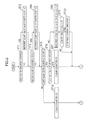
- FIG. 8A is a waveform chart illustrating a result of comparing a PWM signal of a first system and that of a second system in a conventional technique.
- FIG. 8B is a waveform chart illustrating a result of comparing a PWM signal of a first system and that of a second system according to the present invention.
- FIG. 9 is a circuit diagram illustrating another configuration example of the inverter circuit of the first system and the current detecting circuit of FIG. 1 .
- FIG. 10 is a circuit diagram illustrating another configuration example of the inverter circuit of the second system of and the current detecting circuit of FIG. 1 .
- FIG. 11 is a circuit diagram illustrating a configuration example of an inverter circuit of a first system in an electronic control device and a current detecting circuit thereof according to a second embodiment of the present invention.
- FIG. 12 is a circuit diagram illustrating a configuration example of an inverter circuit of a second system in the electronic control device and a current detecting circuit thereof according to the second embodiment of the present invention.
- FIG. 13 is a flowchart partially illustrating a control method for the electronic control device according to the second embodiment of the present invention.
- FIG. 14 is a flowchart partially illustrating a control method for the electronic control device according to the second embodiment of the present invention.
- FIG. 15 is a circuit diagram illustrating another configuration example of the inverter circuit of the first system in the electronic control device according to the second embodiment of the present invention and the current detecting circuit thereof.
- FIG. 16 is a circuit diagram illustrating another configuration example of the inverter circuit of the second system in the electronic control device according to the second embodiment of the present invention and the current detecting circuit thereof.
- FIGS. 1 to 4 illustrate a configuration example of an electronic control device according to a first embodiment of the present invention.
- FIG. 5 is a schematic diagram of an EPS device to which this electronic control device is applied. First, the EPS device is described briefly. Next, described is an electronic control device for controlling a multiphase motor that assists steering force in the EPS device.
- the EPS device is composed of a steering wheel 10 , a steering torque detecting sensor 11 , an assisting multiphase motor 12 , an electronic control device 13 for controlling multiphase motor 12 , and the like. Also, steering torque detecting sensor 11 and a reducer 16 are disposed in a steering column 15 that houses a steering shaft 14 .
- Steering torque detecting sensor 11 detects steering torque that acts on steering shaft 14 during the driver's steering operation, and electronic control device 13 controls driving of multiphase motor 12 based on a steering torque signal S 1 , a vehicle speed signal S 2 , etc., so that multiphase motor 12 can generate steering assist force according to a driving state of the vehicle.
- a pinion gear 17 provided on a tip end of steering shaft 14 is rotated thereby, a rack shaft 18 moves horizontally to the right or left in a travel direction.
- the driver's steering operation is transmitted to a wheel (tire) 19 to turn the vehicle in a desired direction.
- multiphase (in this example, three-phase) motor 12 includes first and second coil sets (muntiphase coil sets of the first and second systems) 12 a , 12 b .
- First coil set 12 a includes a U-phase coil Ua, a V-phase coil Va, and a W-phase coil Wa.
- Second coil set 12 b includes a U-phase coil Ub, a V-phase coil Vb, and a W-phase coil Wb.
- the coil sets 12 a , 12 b can be separately driven by a drive circuit 21 a in a first system of electronic control device 13 and a drive circuit 21 b in a second system thereof, respectively.
- Three-phase motor 12 has a rotor 12 d equipped with an angle sensor 12 e .
- a signal (angle detection signal) S 13 corresponding to a rotational angle of rotor 12 d detected by angle sensor 12 e is input to a microcomputer (CPU) 20 .
- Drive circuit 21 a of the first system is composed of an inverter circuit 22 a , a driver 23 a for inverter circuit 22 a , a capacitor 24 a , a power supply relay (semiconductor relay) 25 a , a driver 26 a for power supply relay 25 a , a current detecting circuit 27 a , and the like.
- Drive circuit 21 a is controlled by microcomputer 20 .
- Microcomputer 20 can also function as a diagnosis apparatus for detecting a failure.
- drive lines (current supply paths) 1 U, 1 V, 1 W between drive circuit 21 a and U-phase coil Ua, V-phase coil Va, and W-phase coil Wa of three-phase motor 12 are provided with phase relays 28 U, 28 V, 28 W that serve as a power supply cutoff element.
- a power supply line 37 a of inverter circuit 22 a is connected to a battery (power supply) BA via power supply relay 25 a .
- Capacitor 24 a is connected between power supply line 37 a and a ground point. Capacitor 24 a assists power supply from battery BA to inverter circuit 22 a and also, eliminates noise components such as surge current.
- As power supply relay 25 a an N-channel MOSFET including a parasitic diode Da is used as power supply relay 25 a .
- Driver 23 a includes H-side driver units corresponding to upper arm switching elements (upstream drive elements) and L-side driver units corresponding to lower arm switching elements (downstream drive elements), which are configured to drive U, V and W phases of inverter circuit 22 a .
- Output terminals of the respective H-side driver units are connected to control terminals of the upper arm switching elements, and microcomputer 20 executes selective ON/OFF control thereof.
- output terminals of the respective L-side driver units are connected to control terminals of the lower arm switching elements, and microcomputer 20 executes selective ON/OFF control thereof.
- an output terminal of driver 26 a is connected to a gate of the N-channel MOSFET that functions as power supply relay 25 a , and microcomputer 20 executes selective ON/OFF control thereof.
- Outputs of inverter circuit 22 a are supplied from drive lines 1 U, 1 V, 1 W to U-phase coil Ua, V-phase coil Va, and W-phase coil Wa of coil set 12 a through drain and source regions of N-channel MOSFETs that function as phase relays 28 U, 28 V, 28 W, respectively.
- phase relays 28 U, 28 V, 28 W are selectively controlled to be ON/OFF by microcomputer 20 to supply current between inverter circuit 22 a and coil set 12 a or cut off current supply therebetween.
- a parasitic diode is formed in a forward direction from the source to the drain.
- a pull up resistor 6 a Connected between U-phase drive line 1 U and battery BA is a pull up resistor 6 a that functions as a potential applying circuit for applying and holding an intermediate potential to drive line 1 U.
- Pull up resistor 6 a is configured to apply an intermediate potential between a voltage of battery BA and the ground potential to U-phase drive line 1 U.
- U-phase drive line 1 U is connected to pull up resistor 6 a but it can be connected to V-phase drive line 1 V or W-phase drive line 1 W.
- Phase potentials of drive lines 1 U, 1 V, 1 W are detected by a phase potential detecting circuit 4 a and the detection result is input to microcomputer 20 .
- drive circuit 21 b of the second system is composed of an inverter circuit 22 b , a driver 23 b for inverter circuit 22 b , a capacitor 24 b , a power supply relay (semiconductor relay) 25 b , a driver 26 b for power supply relay 25 b , current detecting circuit 27 b , and the like.
- Drive circuit 21 b is controlled by microcomputer 20 .
- Drive lines (current supply paths) 2 U, 2 V, 2 W between drive circuit 21 b and U-phase coil Ub, V-phase coil Vb, and W-phase coil Wb of three-phase motor 12 are equipped with phase relays 29 U, 29 V, 29 W that function as a power supply cutoff element.
- Inverter circuit 22 b has a power supply line 37 b connected to battery BA via power supply relay 25 b .
- Capacitor 24 b is connected between power supply line 37 b and the ground point. Capacitor 24 b assists power supply from battery BA to inverter circuit 22 b and eliminates noise components such as surge current.
- As power supply relay 25 b an N-channel MOSFET including a parasitic diode Db is used.
- Driver 23 b includes H-side driver units corresponding to upper arm switching elements (upstream drive elements) for driving the U, V and W phases of inverter circuit 22 b , and L-side driver units corresponding to lower arm switching elements (downstream drive elements) thereof.
- Output terminals of the respective H-side driver units are connected to control terminals of the upper arm switching elements and selectively controlled to be ON/OFF by microcomputer 20 .
- output terminals of the respective L-side driver units are connected to control terminals of the lower arm switching elements, and microcomputer 20 executes selective ON/OFF control thereof.
- an output terminal of driver 26 b is connected to a gate of the N-channel MOSFET that functions as power supply relay 25 b , and microcomputer 20 executes selective ON/OFF control thereof.
- phase relays 29 U, 29 V, 29 W are selectively controlled to be ON/OFF by microcomputer 20 similar to phase relays 28 U, 28 V, 28 W, to thereby supply current between inverter circuit 22 b and coil set 12 b or cut off the current supply.
- MOSFETs as phase relays 29 U, 29 V, 29 W, a parasitic diode is formed in a forward direction from the source to the drain.
- U-phase drive line 2 U Connected between U-phase drive line 2 U and battery BA is a pull up resistor 6 b for applying and holding an intermediate potential to drive line 2 U.
- Pull up resistor 6 b applies an intermediate potential between voltage of battery BA and the ground potential to U-phase drive line 2 U.
- U-phase drive line 2 U is connected to pull up resistor 6 b , but it can be connected to V-phase drive line 2 V or W-phase drive line 2 W.
- Phase potentials of drive lines 2 U, 2 V 2 W are detected by a phase potential detecting circuit 4 b and the detection result is input to microcomputer 20 .
- Microcomputer 20 as a main controller receives steering torque signal S 1 and vehicle speed signal S 2 from the EPS device, and also receives detection signals S 3 to S 8 of current detecting circuits 27 a , 27 b in electronic control device 13 , signals S 9 a to S 11 a and signals S 9 b to S 11 b corresponding to phase potentials detected by phase potential detecting circuits 4 a , 4 b , and the like. Also, microcomputer 20 receives an angle detection signal S 13 from angle sensor 12 e provided in three-phase motor 12 .
- Microcomputer 20 determines whether a short-circuit failure has occurred between coil sets 12 a and 12 b or between inverter circuits 22 a and 22 b based on signals S 3 to S 8 , S 9 a to S 11 a , S 9 b to S 11 b , S 12 a , S 12 b , etc. Then, if no short-circuit failure has occurred, microcomputer 20 controls drive circuits 21 a and 21 b based on signals S 1 , S 2 , S 13 , etc. to drive three-phase motor 12 , so as to generate steering assist force according to a running state of a vehicle.
- FIG. 2 illustrates a configuration example of inverter circuit 22 a and current detecting circuit 27 a of FIG. 1 .
- Inverter circuit 22 a has three-phase bridge circuit configuration with three sets of switching elements for driving U-phase coil Ua, V-phase coil Va, and W-phase coil Wa of three-phase motor 12 on a phase basis via drive lines 1 U, 1 V, 1 W.
- the switching elements are configured by N-channel MOSFETs 31 to 36 .
- Current detecting circuit 27 a is composed of current detecting resistors 38 a to 40 a that function as a current detecting element, and buffers 47 a to 49 a for amplifying voltages (corresponding to currents flowing through the three-phase bridge circuit) detected by current detecting resistors 38 a to 40 a.
- MOSFETs 31 , 32 drain and source regions are series-connected between power supply line 37 a and one end of current detecting resistor 38 a , and their common node is connected to one end of drive line 1 U.
- MOSFETs 33 , 34 drain and source regions are series-connected between power supply line 37 a and one end of current detecting resistor 39 a , and their common node is connected to one end of drive line 1 V.
- MOSFETs 35 and 36 drain and source regions are series-connected between power supply line 37 a and one end of current detecting resistor 40 a , and their common node is connected to one end of drive line 1 W.
- the other ends of current detecting resistors 38 a to 40 a are connected to a negative terminal of the power supply and thus grounded, and voltages detected by current detecting resistors 38 a to 40 a are input to buffers 47 a to 49 a .
- Outputs of buffers 47 a to 49 a are input to microcomputer 20 as detection signals S 3 to S 5 (U-phase current detection value Uai, V-phase current detection value Vai, and W-phase current detection value Wai) corresponding to currents flowing through inverter circuit 22 a.
- diodes D 1 to D 6 connected in the forward direction between the source and drain in MOSFETs 31 to 36 are parasitic diodes.
- FIG. 3 illustrates a configuration example of inverter circuit 22 b and current detecting circuit 27 b of FIG. 1 .
- Inverter circuit 22 b has the same circuit configuration as inverter circuit 22 a , i.e., has three-phase bridge circuit configuration with three sets of switching elements for driving U-phase coil Ub, V-phase coil Vb, and W-phase coil Wb of three-phase motor 12 on a phase basis via drive lines 2 U, 2 V, 2 W. Similar to the above, the switching elements are configured by N-channel MOSFETs 41 to 46 .
- current detecting circuit 27 b is composed of current detecting resistors 38 b to 40 b and buffers 47 b to 49 b for amplifying voltages (corresponding to currents flowing through the three-phase bridge circuit) detected by current detecting resistors 38 b to 40 b , similar to current detecting circuit 27 a.
- MOSFETs 41 , 42 drain and source regions are series-connected between power supply line 37 b and one end of current detecting resistor 38 b , and their common node is connected to one end of drive line 2 U.
- MOSFETs 43 , 44 drain and source regions are series-connected between power supply line 37 b and one end of current detecting resistor 39 b , and their common node is connected to one end of drive line 2 V.
- MOSFETs 45 , 46 drain and source regions are series-connected between power supply line 37 b and one end of current detecting resistor 40 b , and their common node is connected to one end of drive line 2 W.
- Diodes D 7 to D 12 connected in the forward direction between the source and drain in MOSFET 41 to 46 are parasitic diodes.
- FIG. 4 illustrates a configuration example of phase potential detecting circuits 4 a , 4 b of FIG. 1 .
- Phase current detecting circuits 4 a , 4 b detect potentials of drive lines 1 U, 1 V, 1 W, and drive lines 2 U, 2 V, 2 W from inverter circuits 22 a , 22 b to coil sets 12 a , 12 b , respectively, on a phase basis.
- Phase current detecting circuit 4 a is composed of resistors R 1 , R 2 , resistors R 3 , R 4 , and resistors R 5 , R 6 that are series-connected between drive lines 1 U, 1 V, 1 W and the ground point, respectively.
- Phase current detecting circuit 4 b is composed of resistors R 7 , R 8 , resistors R 9 , R 10 , and resistors R 11 , R 12 that are series-connected between drive lines 2 U, 2 V, 2 W and the ground point.
- the potentials at the nodes between resistors R 1 and R 2 , resistors R 3 and R 4 , and resistors R 5 and R 6 are input to microcomputer 20 as signals S 9 a to S 11 a corresponding to detection potentials of U-phase coil Ua, V-phase coil Va, and W-phase coil Wa of coil set 12 a .
- the potentials at the nodes between resistors R 7 and R 8 , resistors R 9 and R 10 , and resistors R 11 and R 12 are input to microcomputer 20 as signals S 9 b to S 11 b corresponding to detection potentials of U-phase coil Ub, V-phase coil Vb, and W-phase coil Wb of coil set 12 b.
- the failure diagnosis operation is started and executed at predetermined time intervals (for example, in milliseconds) during the control of three-phase motor 12 .
- This diagnosis operation is outlined below. That is, a phase of a carrier in the first system is inverted with respect to that in the second system to generate a PWM signal (inverted control signal pulse) for driving inverter circuit 22 a . In other words, the carriers of the first and second systems are made out of phase. Under this condition, when all phases are at low level on the current detection side as a target system while all phases are at high level in the other system, current detection (A/D conversion of a detected current value) is carried out.
- A/D conversion of a current value has to be carried out within periods ⁇ t1 and ⁇ t2 in which a potential difference appears between PWM signals of the first and second systems as illustrated in FIG. 8A .
- This causes an increase in load of a controller.
- a phase of the carrier in the first system is inverted. With this, a midpoint t0 in high period of all phases in the first system matches a midpoint t0 in low period of all phases in the second system. At this timing, current must flow into the first system from the second system.
- MOSFETs 31 , 33 , 35 as upper arm switching elements of all phases in inverter circuit 22 a of the first system are turned ON to apply a high potential to first coil set 12 a , and MOSFETs 42 , 44 , 46 as lower arm switching elements of all phases in inverter circuit 22 b of the second system to control second coil set 12 b to a low potential.
- values of currents flowing through current paths of MOSFETs 42 , 44 , 46 as lower arm switching elements of the inverter circuit 22 b of the second system are detected by current detecting circuit 27 b . If the sum of values in three phases is a predetermined value or more, it is determined that a current supply failure has occurred between the first and second systems.
- inverter circuit 22 a of the first system is executed on inverter circuit 22 b of the second system as well.
- microcomputer 20 outputs a PWM signal to drivers 23 a , 23 b . Also, signals for turning ON power supply relays 25 a , 25 b are output to drivers 26 a , 26 b .
- Each H-side driver and each L-side driver in drivers 23 a , 23 b supply drive signals based on PWM signals to gates of MOSFETs 31 to 36 and 41 to 46 of inverter circuits 22 a , 22 b of the first and second systems based on the PWM signals so as to selectively control the gates to be ON/OFF.
- three-phase motor 12 is driven in three phases by drive circuit 21 a via drive lines 1 U, 1 V, 1 W. Moreover, the motor is driven in three phases by drive circuit 21 b via drive lines 2 U, 2 V, 2 W. At this time, the duty ratio of the PWM signal is varied based on steering torque signal S 1 , vehicle speed signal S 2 , and the like to control an output torque of three-phase motor 12 , thereby changing an assist force.
- step ST 1 it is determined whether the operation of the first system is stopped. If the operation is stopped, a count value C 1 a of a stop transition counter C 1 of the first system is incremented by “+1” (step ST 2 ). If the operation is not stopped, it is determined whether the operation of the second system is stopped (step ST 3 ).
- step ST 4 a count value C 2 b of a stop transition counter C 2 of the second system is incremented by “+1” (step ST 4 ). If the operation is not stopped, it is determined whether count value C 2 b of stop transition counter C 2 of the second system is 0 or 5 (step ST 5 ).
- step ST 5 it is determined whether the sum of U-phase current detection value Uai, V-phase current detection value Vai, and W-phase current detection value Wai in current detecting circuit 27 a of the first system is 5 A (5 amp) or less, that is, “Uai+Vai+Wai ⁇ 5 A” (step ST 6 ). Then, if “Uai+Vai+Wai ⁇ 5 A”, an abnormality counter C 3 of the first system is cleared (step ST 7 ). If “Uai+Vai+Wai>5 A”, a count value C 3 a of abnormality counter C 3 of the first system is incremented by “+1” (step ST 8 ). After abnormality counter C 3 of the first system is cleared in step ST 7 , the processing proceeds to step ST 12 of FIG. 7 to determine whether count value C 1 a of stop transition counter C 1 of the first system is 0 or 5.
- step ST 9 count value C 3 a of abnormality counter C 3 of the first system satisfies “C 3 a ⁇ 5”. If “C 3 a ⁇ 5”, the operation of the first system is stopped (step ST 10 ). The operation of the first system is stopped by, for example, turning OFF MOSFETs 31 to 36 of inverter circuit 22 a to control the output of inverter circuit 22 a to a high impedance. If “C 3 a ⁇ 5”, the processing proceeds to step ST 12 .
- step ST 11 If it is determined that count value C 2 b is not 0 or 5 in step ST 5 above, abnormality counter C 3 of the first system is cleared and the processing proceeds to step ST 13 of FIG. 7 (step ST 11 ).
- step ST 12 it is determined whether count value C 1 a of stop transition counter C 1 of the first system is 0 or 5. If it is determined that count value C 1 a is 0 or 5, it is determined whether the sum of U-phase current detection value Ubi, V-phase current detection value Vbi, and W-phase current detection value Wbi in current detecting circuit 27 b of the second system is 5 A (5 amp) or less, that is, “Ubi+Vbi+Wbi ⁇ 5 A” (step ST 13 ). Then, if “Ubi+Vbi+Wbi ⁇ 5 A”, abnormality counter C 4 of the second system is cleared and the processing is terminated (step ST 14 ).
- step ST 15 it is determined whether count value C 4 b of abnormality counter C 4 of the second system satisfies “C 4 b ⁇ 5”. If “C 4 b ⁇ 5”, the operation of the second system is stopped and the processing is terminated (step ST 17 ). If “C 4 b ⁇ 5”, the processing is terminated at this point. The operation of the second system is stopped by, for example, turning OFF MOSFETs 41 to 46 of inverter circuit 22 b to control the output of inverter circuit 22 b to a high impedance.
- step ST 18 If it is determined that count value C 1 a is not 0 or 5 in step ST 12 above, abnormality counter C 4 of the second system is cleared and the processing is terminated (step ST 18 ).
- microcomputer 20 turns OFF all MOSFETs 31 to 36 of inverter circuit 22 a to hold the output at a high impedance and then, executes motor control operation with drive circuit 21 b of the second system. Alternatively, it turns OFF phase relays 28 U, 28 V, 28 W so that no drive current is supplied from inverter circuit 22 a to coil set 12 a.
- the microcomputer turns OFF all MOSFETs 41 to 46 of inverter circuit 22 b to hold the output at a high impedance and then, executes a motor control operation with drive circuit 21 a of the first system. Alternatively, it turns OFF phase relays 29 U, 29 V, 29 W so that no drive current is supplied from inverter circuit 22 b to coil set 12 b.
- the steering assist force generated by either drive circuit 21 a or drive circuit 21 b is reduced to 1 ⁇ 2 of that generated by both of them. Nevertheless, since the assist operation can be continued, the degradation in safety, caused by sudden stop of assist operation, can be suppressed.
- a power supply failure determination which is executed based on a current value in the other system, is stopped for a predetermined period.
- a diagnosis may be stopped for a predetermined period by turning ON MOSFETs 31 , 33 , 35 as upper arm switching elements of all phases in inverter circuit 22 a of the second system to hold a high potential under control and also, by turning ON MOSFETs 42 , 44 , 46 as lower arm switching elements of all phases in the first system to hold a low potential under control.
- the predetermined period indicates the time until the opposing inverter circuit (the other inverter circuit) stops operation and current supply is stopped.
- the microcomputer waits the predetermined period before confirmation about a failure of own system. After current supply is stopped, the microcomputer may confirm whether own system has failed.
- This processing is to A/D convert current values detected at midpoints of low outputs of the first and second systems.
- current flows in both directions at some timing and it is detected that a failure has occurred in the respective systems.
- the other system is placed in a standby state. Then, the current values of the first and second systems are detected. If a short-circuit failure has occurred, current flows from the first system to the second system and also from the second system to the first system. Thus, only when an abnormality has been found on the both sides, it is determined that an intergate short-circuit has occurred, and one of the two systems is stopped.
- FIGS. 9 and 10 illustrate another configuration example of inverter circuits 22 a , 22 b of the first and second systems, and current detecting circuits 27 a , 27 b thereof illustrated in FIGS. 2 and 3 .
- FIGS. 2 and 3 illustrate a downstream shunt system in which current detecting circuits 27 a , 27 b are provided between inverter circuits 22 a , 22 b and the ground point, respectively.
- FIGS. 9 and 10 illustrate an upstream shunt system in which current detecting circuits 27 a , 27 b are provided between power supply lines 37 a , 37 b (positive terminals of the power supply) and inverter circuits 22 a , 22 b , respectively.
- a phase of the carrier of the first system is inverted to generate a PWM signal for driving the inverter circuit, whereby an abnormal current caused by intersystem short-circuit can be reliably detected. Furthermore, since the timing of current detection and subsequent A/D conversion can be the same as the A/D conversion (value at midpoint of low output period) for power supply control, an increase in processing load on the microcomputer can be minimized.
- FIGS. 11 and 12 illustrate an electronic control device according to a second embodiment of the present invention.
- FIGS. 1I and 12 are circuit diagrams illustrating configuration examples of inverter circuits 22 a , 22 b of the first and second systems in FIG. 1 and current detecting circuits 27 a , 27 b thereof.
- current detecting circuit 27 a is configured of current detecting resistor 38 a , buffer 47 a , and peak hold circuit 50 a
- current detecting circuit 27 b is configured of current detecting resistor 38 b , buffer 47 b , and peak hold circuit 50 b.
- inverter circuit 22 a of the first system has the same configuration as in FIG. 2 , and current detecting resistor 38 a is connected between inverter circuit 22 a and the ground point.
- a voltage detected by the current detecting resistor 38 a is input to buffer 47 a .
- the output of buffer 47 a is input to microcomputer 20 as detection signal S 3 corresponding to current flowing in inverter circuit 22 a and also input to peak hold circuit 50 a , and a peak value is input to microcomputer 20 as detection signal S 4 .
- inverter circuit 22 b of the second system has the same configuration as in FIG. 11 , and current detecting resistor 38 b is connected between inverter circuit 22 b and the ground point.
- a voltage detected by current detecting resistor 38 b is input to buffer 47 b .
- the output of buffer 47 b is input to microcomputer 20 as detection signal S 5 corresponding to current flowing in inverter circuit 22 b and also input to peak hold circuit 50 b , and a peak value is input to microcomputer 20 as detection signal S 6 .
- the failure diagnosis operation based on the control method of the second embodiment is started and executed at predetermined time intervals (for example, in milliseconds) during control of the three-phase motor similar to the first embodiment.
- MOSFETs 31 , 33 , 35 as upper arm switching elements of all phases in inverter circuit 22 a of the first system are turned ON to apply a high potential to first coil set 12 a and MOSFETs 42 , 44 , 46 as lower arm switching elements of all phases in inverter circuit 22 b of the second system are turned ON to control second coil set 12 b to a low potential.
- current detecting circuit 27 b detects values of currents flowing through current paths of MOSFETs 41 , 43 , 45 as upper arm switching elements of inverter circuit 22 b of the second system and MOSFETs 42 , 44 , 46 as lower arm switching elements thereof. Then, if a 1N shunt current detection value is a predetermined value or more, it is determined that a power supply failure has occurred between the first and second systems.
- step ST 21 it is determined whether the operation of the first system is stopped. If the operation is stopped, count value C 1 a of stop transition counter C 1 of the first system is incremented by “+1” (step ST 22 ), or otherwise, it is determined whether the operation of the second system is stopped (step ST 23 ).
- step ST 23 If it is determined that the operation is stopped in step ST 23 , count value C 2 b of stop transition counter C 2 of the second system is incremented by “+1” (step ST 24 ), or otherwise, it is determined whether the count value C 2 b of stop transition counter C 2 of the second system is 0 or 5 (step ST 25 ).
- step ST 25 If it is determined in step ST 25 that count value C 2 b is 0 or 5, it is determined whether a current detection value (1N shunt current detection value) in current detecting circuit 27 a of the first system is 100 A (100 amp) or less (step ST 26 ). Then, if the value is 100 A or less, abnormality counter C 3 of the first system is cleared (step ST 27 ), whereas if the value is not 100 A or less, count value C 3 a of abnormality counter C 3 of the first system is incremented by “+1” (step ST 28 ). After abnormality counter C 3 of the first system is cleared in step ST 27 , the processing moves to step ST 32 of FIG. 14 to determine whether count value C 1 a of stop transition counter C 1 of the first system is 0 or 5.
- step ST 29 it is determined whether count value C 3 a of abnormality counter C 3 of the first system satisfies “C 3 a ⁇ 5”, and if “C 3 a ⁇ 5”, the operation of the first system is stopped (step ST 30 ). If “C 3 a ⁇ 5” is not satisfied, the processing moves to step ST 32 .
- step ST 25 If it is determined in step ST 25 that count value C 2 b is not 0 or 5, abnormality counter C 3 of the first system is cleared, and the processing moves to step ST 33 of FIG. 14 (step ST 31 ).
- step ST 32 it is determined whether count value C 1 a of stop transition counter C 1 of the first system is 0 or 5, and if it is determined that count value Ca is 0 or 5, it is determined whether a current detection value (1N shunt current detection value) in current detecting circuit 27 b of the second system is 100 A (100 amp) or less (step ST 33 ). Then, if the value is 100 A or less, abnormality counter C 4 of the second system is cleared and the processing is terminated (step ST 34 ).
- step ST 35 it is determined whether count value C 4 b of abnormality counter C 4 of the second system satisfies “C 4 b ⁇ 5”. If “C 4 b ⁇ 5”, the operation of the second system is stopped and then, the processing is terminated (step ST 37 ). If “C 4 b ⁇ 5”, the processing is terminated at this point.
- step ST 32 If it is determined in step ST 32 that count value C 1 a is not 0 or 5, abnormality counter C 4 of the second system is cleared and the processing is terminated (step ST 38 ).
- microcomputer 20 turns OFF all MOSFETs 31 to 36 of inverter circuit 22 a and holds the output at a high impedance and in this state, executes the motor control operation with drive circuit 21 b of the second system. Alternatively, it turns OFF phase relays 28 U, 28 V, 28 W not to supply a drive current from inverter circuit 22 a to coil set 12 a.
- the microcomputer turns OFF all MOSFETs 41 to 46 of inverter circuit 22 b and holds the output at a high impedance and in this state, executes a motor control operation with drive circuit 21 a of the first system. Alternatively, it turns OFF phase relays 29 U, 29 V, 29 W not to supply a drive current from inverter circuit 22 b to coil set 12 b.
- the steering assist force generated by either drive circuit 21 a or drive circuit 21 b is reduced to 1 ⁇ 2 of that generated by both of them. Nevertheless, since the assist operation can be continued, the degradation in safety, caused by sudden stop of assist operation, can be suppressed.
- FIGS. 15 and 16 illustrate another configuration example of inverter circuits 22 a , 22 b of the first and second systems and current detecting circuits 27 a , 27 b thereof illustrated in FIGS. 11 and 12 , respectively.
- FIGS. 11 and 12 illustrate a downstream shunt system in which current detecting circuits 27 a , 27 b are provided between inverter circuits 22 a , 22 b and the ground point, respectively.
- FIGS. 15 and 16 illustrate an upstream shunt system in which current detecting circuits 27 a , 27 b are provided between power supply lines 37 a , 37 b and inverter circuits 22 a , 22 b , respectively.
- the other basic configuration is the same as those in FIGS.
- control method for the electronic control device according to the second embodiment of the present invention can also provide substantially the same operational effects as in the first embodiment.
- the electronic control device is applied to the EPS device.
- it can be applied to any other types of devices or systems for driving a multiphase motor with inverter circuits of the two systems (or plural systems), such as a steer-by-wire device as well as the EPS device.
- the inverter circuits of the two systems are controlled by one microcomputer.
- the electronic control device has the phase relay between each inverter circuit and the coils of the motor.
- the present invention is also applicable to an electronic control device having no phase relay.
- one semiconductor element for the phase relay is provided in each phase.
- the present invention is also applicable to such a configuration that a phase relay has two semiconductor elements with oppositely formed parasitic diodes.
- the carrier for the upper arm switching element in the inverter circuit of the first system is inverted and a center value of the inverted control signal pulse is approximated to a value at midpoint of low potential period of all phases in the inverter circuit of the second system.
- substantially the same operation effects can be achieved by, for example, setting coil sets 12 a and 12 b of three-phase motor 12 substantially 180 degrees out of phase. If the coils are substantially 180 degrees out of phase, voltage phases are opposite to each other. Thus, if the voltage (amplitude of the voltage) of the first system increases, that of the second system decreases, whereby a timing of current detection is expanded.
- MOSFET Metal Oxide Semiconductor Field Effect Transistor
- IGBT Insulated Gate Bipolar Transistor
- One mode of the present invention is an electronic control device for driving a motor including multiphase coil sets of first and second systems, including inverter circuits of the first and second systems, which include upper arm switching elements and lower arm switching elements which are provided for each of phases of the multiphase coil sets of the first and second systems and selectively controlled to be ON/OFF, in which the upper arm switching elements or lower arm switching elements of all phases in the inverter circuit of the first system are turned ON and the lower arm switching elements or upper arm switching elements of all phases in the inverter circuit of the second system are turned ON, and in this state, it is determined whether a power supply failure has occurred between the first and second systems based on a value of current flowing through the lower arm switching element or upper arm switching element in the inverter circuit of the second system.
- the upper arm switching elements or lower arm switching elements of all phases in the inverter circuit of the second system are turned ON and the lower arm switching elements or upper arm switching elements of all phases in the inverter circuit of the first system are turned ON and in this state, it is determined whether a power supply failure has occurred between the first and second systems based on a value of current flowing through the lower arm switching element or upper arm switching element in the inverter circuit of the first system.
- a PWM carrier signal for a switching element of the inverter circuit in the first system is substantially 180 degrees out of phase from a PWM carrier signal for a switching element of the inverter circuit in the second system.
- the multiphase coil sets of the first and second systems are disposed with a phase difference of substantially 180 degrees in electric angle.
- a current detecting element is provided between a lower arm switching element of at least one phase in each system and a negative terminal of the power supply.
- a current detecting element is provided between a lower arm switching element of each phase in each system and a negative terminal of the power supply.
- a current detecting element is provided between an upper arm switching element of at least one phase in each system and a positive terminal of the power supply.
- a current detecting element is provided between an upper arm switching element of each phase in each system and a negative terminal of the power supply.
- a current detecting element is provided between a motor coil and a node between upper and lower arm switching elements of at least one phase in each system.
- a current detecting element is provided between a motor coil and a node between upper and lower arm switching elements of each phase in each system.
- the upper and lower arm switching elements of all phases in the inverter of the first or second system are controlled to be OFF.
- the upper and lower arm switching elements of all phases in the inverter of the system that has been determined to have abnormal current are controlled to be OFF.
- the multiphase motor is for electric power steering devices or for steer-by-wire control.
- one mode of the present invention is a control method for an electronic control device that drives a motor including multiphase coil sets of first and second systems, and includes inverter circuits of the first and second systems, including upper arm switching elements and lower arm switching elements which are provided for each of phases of the multiphase coil sets of the first and second systems of the motor and selectively controlled to be ON/OFF, the method including the steps of: turning ON the upper arm switching elements or lower arm switching elements of all phases in the inverter circuit of the first system and turning ON the lower arm switching elements or upper arm switching elements of all phases in the inverter circuit of the second system; detecting a value of current flowing through the lower arm switching element or upper arm switching element in the inverter circuit of the second system; and determining whether a power supply failure has occurred between the first and second systems based on the detected value of current.
- the step of determining whether a power supply failure has occurred between the first and second systems when the detected value of current or the sum of current values in all phases is a predetermined value or more, it is determined that a power supply failure has occurred between the first and second systems.
Landscapes
- Engineering & Computer Science (AREA)
- Power Engineering (AREA)
- Chemical & Material Sciences (AREA)
- Combustion & Propulsion (AREA)
- Transportation (AREA)
- Mechanical Engineering (AREA)
- Inverter Devices (AREA)
- Control Of Ac Motors In General (AREA)
- Control Of Electric Motors In General (AREA)
Abstract
Description
- Patent Document 1: JP 2011-152027 A
- Patent Document 2: JP 2014-176229 A
- 1U, 1V, 1W, 2U, 2V, 2W Drive line
- 4 a, 4 b Phase potential detecting circuit
- 6 a, 6 b Pull up resistor
- 12 Three-phase motor (multiphase motor)
- 12 a, 12 b Coil set
- 13 Electronic control device
- 20 Microcomputer (controller)
- 21 a, 21 b Drive circuit
- 22 a, 22 b Inverter circuit
- 23 a, 23 b Driver
- 25 a, 25 b Power supply relay
- 27 a, 27 b Current detecting circuit
- 28U, 28V, 28W, 29U, 29V, 29W Phase relay
- 31 to 36, 41 to 46 MOSFET
Claims (20)
Applications Claiming Priority (3)
| Application Number | Priority Date | Filing Date | Title |
|---|---|---|---|
| JP2016053517A JP6533754B2 (en) | 2016-03-17 | 2016-03-17 | Electronic control device and control method thereof |
| JP2016-053517 | 2016-03-17 | ||
| PCT/JP2016/073267 WO2017158861A1 (en) | 2016-03-17 | 2016-08-08 | Electronic control device and control method thereof |
Publications (2)
| Publication Number | Publication Date |
|---|---|
| US20190089288A1 US20190089288A1 (en) | 2019-03-21 |
| US10404202B2 true US10404202B2 (en) | 2019-09-03 |
Family
ID=59852201
Family Applications (1)
| Application Number | Title | Priority Date | Filing Date |
|---|---|---|---|
| US16/083,845 Active US10404202B2 (en) | 2016-03-17 | 2016-08-08 | Electronic control device and control method thereof |
Country Status (6)
| Country | Link |
|---|---|
| US (1) | US10404202B2 (en) |
| JP (1) | JP6533754B2 (en) |
| KR (1) | KR101958160B1 (en) |
| CN (1) | CN108702129B (en) |
| DE (1) | DE112016006613B4 (en) |
| WO (1) | WO2017158861A1 (en) |
Families Citing this family (2)
| Publication number | Priority date | Publication date | Assignee | Title |
|---|---|---|---|---|
| CN108604875B (en) * | 2016-02-17 | 2022-02-01 | 三菱电机株式会社 | Power conversion device |
| EP4047809A1 (en) * | 2021-02-22 | 2022-08-24 | Hamilton Sundstrand Corporation | Control distribution architecture |
Citations (7)
| Publication number | Priority date | Publication date | Assignee | Title |
|---|---|---|---|---|
| JP2011152027A (en) | 2009-12-25 | 2011-08-04 | Denso Corp | Motor drive apparatus, and electric power steering apparatus using the same |
| US20130257332A1 (en) | 2012-03-29 | 2013-10-03 | Kosuke Nakano | Electric motor driving apparatus having failure detection circuit, and failure detection method for the electric motor driving apparatus having failure detection circuit |
| US20140253006A1 (en) | 2013-03-11 | 2014-09-11 | Denso Corporation | Power converter |
| JP2015173554A (en) | 2014-03-12 | 2015-10-01 | 日立オートモティブシステムズ株式会社 | Motor controller |
| US20170346436A1 (en) * | 2016-05-27 | 2017-11-30 | Denso Corporation | Control apparatus of rotary electric machine and electric power steering apparatus using the same |
| US20190023315A1 (en) * | 2016-03-14 | 2019-01-24 | Mitsubishi Electric Corporation | Electric motor control system and electric power steering apparatus therewith |
| US20190077449A1 (en) * | 2016-03-04 | 2019-03-14 | Nidec Corporation | Power conversion device, motor drive unit, electric power steering device, and relay module |
Family Cites Families (8)
| Publication number | Priority date | Publication date | Assignee | Title |
|---|---|---|---|---|
| JP2884942B2 (en) | 1992-09-17 | 1999-04-19 | 株式会社日立製作所 | Electric car control device |
| JP4831503B2 (en) | 2009-09-30 | 2011-12-07 | 株式会社デンソー | Control device for multi-phase rotating machine and electric power steering device using the same |
| JP5045799B2 (en) | 2010-08-27 | 2012-10-10 | 株式会社デンソー | Power conversion device, drive device, and electric power steering device using the same |
| JP5622053B2 (en) * | 2012-02-09 | 2014-11-12 | 株式会社デンソー | Control device for multi-phase rotating machine and electric power steering device using the same |
| JP5614661B2 (en) | 2012-10-09 | 2014-10-29 | 株式会社デンソー | Rotating electrical machine control device and electric power steering device using the same |
| JP5790733B2 (en) | 2013-10-22 | 2015-10-07 | 株式会社デンソー | Power supply current monitoring device |
| JP2015104240A (en) | 2013-11-26 | 2015-06-04 | 株式会社デンソー | Rotary electric machine driving device, and electric power steering device using the same |
| JP6211443B2 (en) | 2014-03-14 | 2017-10-11 | 日立オートモティブシステムズ株式会社 | Electric motor control device |
-
2016
- 2016-03-17 JP JP2016053517A patent/JP6533754B2/en active Active
- 2016-08-08 DE DE112016006613.9T patent/DE112016006613B4/en active Active
- 2016-08-08 CN CN201680082750.5A patent/CN108702129B/en active Active
- 2016-08-08 US US16/083,845 patent/US10404202B2/en active Active
- 2016-08-08 WO PCT/JP2016/073267 patent/WO2017158861A1/en active Application Filing
- 2016-08-08 KR KR1020187025583A patent/KR101958160B1/en active IP Right Grant
Patent Citations (9)
| Publication number | Priority date | Publication date | Assignee | Title |
|---|---|---|---|---|
| JP2011152027A (en) | 2009-12-25 | 2011-08-04 | Denso Corp | Motor drive apparatus, and electric power steering apparatus using the same |
| US20130257332A1 (en) | 2012-03-29 | 2013-10-03 | Kosuke Nakano | Electric motor driving apparatus having failure detection circuit, and failure detection method for the electric motor driving apparatus having failure detection circuit |
| JP2013207975A (en) | 2012-03-29 | 2013-10-07 | Mitsubishi Electric Corp | Motor driving device with failure detection circuit, and failure detection method for motor driving device |
| US20140253006A1 (en) | 2013-03-11 | 2014-09-11 | Denso Corporation | Power converter |
| JP2014176229A (en) | 2013-03-11 | 2014-09-22 | Denso Corp | Power conversion device |
| JP2015173554A (en) | 2014-03-12 | 2015-10-01 | 日立オートモティブシステムズ株式会社 | Motor controller |
| US20190077449A1 (en) * | 2016-03-04 | 2019-03-14 | Nidec Corporation | Power conversion device, motor drive unit, electric power steering device, and relay module |
| US20190023315A1 (en) * | 2016-03-14 | 2019-01-24 | Mitsubishi Electric Corporation | Electric motor control system and electric power steering apparatus therewith |
| US20170346436A1 (en) * | 2016-05-27 | 2017-11-30 | Denso Corporation | Control apparatus of rotary electric machine and electric power steering apparatus using the same |
Also Published As
| Publication number | Publication date |
|---|---|
| DE112016006613T5 (en) | 2018-11-29 |
| JP6533754B2 (en) | 2019-06-19 |
| KR20180103175A (en) | 2018-09-18 |
| WO2017158861A1 (en) | 2017-09-21 |
| KR101958160B1 (en) | 2019-03-13 |
| DE112016006613B4 (en) | 2022-10-13 |
| CN108702129A (en) | 2018-10-23 |
| CN108702129B (en) | 2020-02-18 |
| JP2017169383A (en) | 2017-09-21 |
| US20190089288A1 (en) | 2019-03-21 |
Similar Documents
| Publication | Publication Date | Title |
|---|---|---|
| US10421482B2 (en) | Electronic control unit and control method for the same | |
| KR101662480B1 (en) | Electric motor control device and control method | |
| US8232752B2 (en) | Electric motor control apparatus | |
| EP3193443B1 (en) | Inverter device for driving multi-phase ac motor | |
| US10093351B2 (en) | Electronic control unit and electric power steering apparatus equipped with the same | |
| US9806643B2 (en) | Drive control apparatus for electric motor | |
| EP2755314B1 (en) | Switch driving circuit, inverter apparatus and power steering apparatus | |
| US20170085205A1 (en) | Controller and control method for motor | |
| US20160028336A1 (en) | Control apparatus for electric motor and control method for electric motor | |
| US20110068728A1 (en) | Motor drive device | |
| US9806648B2 (en) | Motor control device and electric power steering system | |
| US20150280609A1 (en) | Load driving device | |
| US20190393825A1 (en) | Failure diagnosis method for inverter circuit | |
| JP2013198202A (en) | Inverter device and power steering device | |
| US10071762B2 (en) | Detection and mitigation of inverter errors in steering system motors | |
| US11183963B2 (en) | Abnormality detection device | |
| US9831807B2 (en) | Motor control apparatus and power steering system | |
| US10924054B2 (en) | Failure diagnosis method for inverter circuit | |
| US10574171B2 (en) | Inductive load control device | |
| EP3367548A1 (en) | Inverter circuit, motor controller, and power steering system | |
| US10404202B2 (en) | Electronic control device and control method thereof | |
| JP6445900B2 (en) | Electric power steering device | |
| JP2018160972A (en) | Control device of motor drive circuit and diagnostic method of motor drive circuit | |
| JP6131874B2 (en) | Inverter circuit failure detection method, drive device, and motor drive system |
Legal Events
| Date | Code | Title | Description |
|---|---|---|---|
| FEPP | Fee payment procedure |
Free format text: ENTITY STATUS SET TO UNDISCOUNTED (ORIGINAL EVENT CODE: BIG.); ENTITY STATUS OF PATENT OWNER: LARGE ENTITY |
|
| AS | Assignment |
Owner name: HITACHI AUTOMOTIVE SYSTEMS, LTD., JAPAN Free format text: ASSIGNMENT OF ASSIGNORS INTEREST;ASSIGNORS:KOSEKI, TOMONOBU;YATSUGI, TOMISHIGE;IIJIMA, FUMIYA;SIGNING DATES FROM 20180730 TO 20180803;REEL/FRAME:046833/0455 |
|
| STPP | Information on status: patent application and granting procedure in general |
Free format text: DOCKETED NEW CASE - READY FOR EXAMINATION |
|
| STPP | Information on status: patent application and granting procedure in general |
Free format text: NOTICE OF ALLOWANCE MAILED -- APPLICATION RECEIVED IN OFFICE OF PUBLICATIONS |
|
| STPP | Information on status: patent application and granting procedure in general |
Free format text: PUBLICATIONS -- ISSUE FEE PAYMENT VERIFIED |
|
| STCF | Information on status: patent grant |
Free format text: PATENTED CASE |
|
| AS | Assignment |
Owner name: HITACHI ASTEMO, LTD., JAPAN Free format text: CHANGE OF NAME;ASSIGNOR:HITACHI AUTOMOTIVE SYSTEMS, LTD.;REEL/FRAME:056299/0447 Effective date: 20210101 |
|
| MAFP | Maintenance fee payment |
Free format text: PAYMENT OF MAINTENANCE FEE, 4TH YEAR, LARGE ENTITY (ORIGINAL EVENT CODE: M1551); ENTITY STATUS OF PATENT OWNER: LARGE ENTITY Year of fee payment: 4 |