US10248155B2 - Semiconductor device including clock generating circuit and channel management circuit - Google Patents
Semiconductor device including clock generating circuit and channel management circuit Download PDFInfo
- Publication number
- US10248155B2 US10248155B2 US15/415,041 US201715415041A US10248155B2 US 10248155 B2 US10248155 B2 US 10248155B2 US 201715415041 A US201715415041 A US 201715415041A US 10248155 B2 US10248155 B2 US 10248155B2
- Authority
- US
- United States
- Prior art keywords
- clock
- circuit
- request signal
- unit
- channel management
- Prior art date
- Legal status (The legal status is an assumption and is not a legal conclusion. Google has not performed a legal analysis and makes no representation as to the accuracy of the status listed.)
- Active, expires
Links
Images


Classifications
-
- G—PHYSICS
- G06—COMPUTING; CALCULATING OR COUNTING
- G06F—ELECTRIC DIGITAL DATA PROCESSING
- G06F1/00—Details not covered by groups G06F3/00 - G06F13/00 and G06F21/00
- G06F1/04—Generating or distributing clock signals or signals derived directly therefrom
- G06F1/06—Clock generators producing several clock signals
-
- G—PHYSICS
- G06—COMPUTING; CALCULATING OR COUNTING
- G06F—ELECTRIC DIGITAL DATA PROCESSING
- G06F1/00—Details not covered by groups G06F3/00 - G06F13/00 and G06F21/00
- G06F1/26—Power supply means, e.g. regulation thereof
- G06F1/32—Means for saving power
- G06F1/3203—Power management, i.e. event-based initiation of a power-saving mode
- G06F1/3234—Power saving characterised by the action undertaken
- G06F1/3237—Power saving characterised by the action undertaken by disabling clock generation or distribution
-
- Y—GENERAL TAGGING OF NEW TECHNOLOGICAL DEVELOPMENTS; GENERAL TAGGING OF CROSS-SECTIONAL TECHNOLOGIES SPANNING OVER SEVERAL SECTIONS OF THE IPC; TECHNICAL SUBJECTS COVERED BY FORMER USPC CROSS-REFERENCE ART COLLECTIONS [XRACs] AND DIGESTS
- Y02—TECHNOLOGIES OR APPLICATIONS FOR MITIGATION OR ADAPTATION AGAINST CLIMATE CHANGE
- Y02D—CLIMATE CHANGE MITIGATION TECHNOLOGIES IN INFORMATION AND COMMUNICATION TECHNOLOGIES [ICT], I.E. INFORMATION AND COMMUNICATION TECHNOLOGIES AIMING AT THE REDUCTION OF THEIR OWN ENERGY USE
- Y02D10/00—Energy efficient computing, e.g. low power processors, power management or thermal management
-
- Y02D10/128—
-
- Y—GENERAL TAGGING OF NEW TECHNOLOGICAL DEVELOPMENTS; GENERAL TAGGING OF CROSS-SECTIONAL TECHNOLOGIES SPANNING OVER SEVERAL SECTIONS OF THE IPC; TECHNICAL SUBJECTS COVERED BY FORMER USPC CROSS-REFERENCE ART COLLECTIONS [XRACs] AND DIGESTS
- Y02—TECHNOLOGIES OR APPLICATIONS FOR MITIGATION OR ADAPTATION AGAINST CLIMATE CHANGE
- Y02D—CLIMATE CHANGE MITIGATION TECHNOLOGIES IN INFORMATION AND COMMUNICATION TECHNOLOGIES [ICT], I.E. INFORMATION AND COMMUNICATION TECHNOLOGIES AIMING AT THE REDUCTION OF THEIR OWN ENERGY USE
- Y02D30/00—Reducing energy consumption in communication networks
- Y02D30/50—Reducing energy consumption in communication networks in wire-line communication networks, e.g. low power modes or reduced link rate
-
- Y02D50/20—
Definitions
- Exemplary embodiments of the present disclosure relate to a semiconductor device including a semiconductor circuit.
- SoCs system-on-chips
- SoCs may be implemented into a form in which conventional multi-functional blocks such as, for example, intellectual property (IP) blocks, are integrated on a single chip.
- IP intellectual property
- SoCs increase in integration density and size, and as the operating speed thereof is improved, low power consumption becomes an important factor, since high power consumption may raise the temperature of a chip, resulting in the SoC malfunctioning or the SoC being damaged.
- a semiconductor device includes a first clock generating circuit including a first control circuit and a first clock gating circuit, a first channel management circuit which communicates with the first clock generating circuit according to a full handshake method, a second clock generating circuit including a second control circuit and a second clock gating circuit, and a second channel management circuit which communicates with the second clock generating circuit according to the full handshake method.
- the first clock gating circuit outputs a first clock
- the second clock gating circuit outputs a second clock different from the first clock.
- a semiconductor device includes a first clock generating circuit including a first control circuit and a first clock gating circuit, a first channel management circuit which communicates with the first clock generating circuit according to a full handshake method, and a second clock generating circuit including a second control circuit and a second clock gating circuit.
- the second clock generating circuit communicates with the first channel management circuit according to the full handshake method.
- the first clock gating circuit outputs a first clock
- the second clock gating circuit outputs a second clock different from the first clock.
- a semiconductor device includes a first clock generating circuit including a first control circuit and a first clock gating circuit, a first channel management circuit which communicates with the first clock generating circuit according to a full handshake method, and a second channel management circuit which communicates with the first clock generating circuit according to the full handshake method.
- the first channel management circuit transmits a first clock request signal to the first clock generating circuit
- the second channel management circuit transmits a second clock request signal to the first clock generating circuit.
- FIG. 1 is a block diagram illustrating a semiconductor device according to exemplary embodiments of the present disclosure.
- FIG. 2 is a block diagram illustrating a clock management unit included in a semiconductor device according to exemplary embodiments of the present disclosure.
- FIG. 3 is a block diagram illustrating an intellectual property (IP) block included in a semiconductor device according to exemplary embodiments of the present disclosure.
- IP intellectual property
- FIG. 4 illustrates a signal transmission path among a plurality of control circuits according to exemplary embodiments of the present disclosure.
- FIG. 5A illustrates a clock request signal and a clock acknowledgement signal used in exemplary embodiments of the present disclosure.
- FIG. 5B illustrates a clock level transition for the clock request signal and the clock acknowledgement signal used in exemplary embodiments of the present disclosure.
- FIG. 6 is a block diagram illustrating a semiconductor device according to exemplary embodiments of the present disclosure.
- FIG. 7 is a block diagram illustrating a semiconductor device according to exemplary embodiments of the present disclosure.
- FIG. 8 is a block diagram illustrating a semiconductor device according to exemplary embodiments of the present disclosure.
- FIG. 9A is a block diagram illustrating a semiconductor device according to exemplary embodiments of the present disclosure.
- FIG. 9B is a timing diagram illustrating an operation of the semiconductor device of FIG. 9A according to exemplary embodiments of the present disclosure.
- FIG. 10A is a block diagram illustrating a semiconductor device according to exemplary embodiments of the present disclosure.
- FIG. 10B is a timing diagram illustrating an operation of the semiconductor device of FIG. 10A according to exemplary embodiments of the present disclosure.
- FIG. 11 is a block diagram illustrating a semiconductor device according to exemplary embodiments of the present disclosure.
- FIG. 12 is a block diagram illustrating a semiconductor device according to exemplary embodiments of the present disclosure.
- FIG. 13 is a block diagram illustrating a semiconductor device according to exemplary embodiments of the present disclosure.
- FIG. 14 is a block diagram illustrating a semiconductor device according to exemplary embodiments of the present disclosure.
- FIG. 15 is a block diagram illustrating an embodiment of a semiconductor system including a semiconductor device according to exemplary embodiments of the present disclosure.
- FIG. 16 is a block diagram illustrating an embodiment of a semiconductor system including a semiconductor device according to exemplary embodiments of the present disclosure.
- each of the units described herein may be implemented as and referred to as circuits (e.g., a clock MUX unit be implemented as a circuit and referred to as a clock MUX circuit, a clock gating unit may be implemented as a circuit and referred to as a clock gating circuit, a channel management unit may be implemented as a circuit and referred to as a channel management circuit, etc.).
- a clock MUX unit be implemented as a circuit and referred to as a clock MUX circuit
- a clock gating unit may be implemented as a circuit and referred to as a clock gating circuit
- a channel management unit may be implemented as a circuit and referred to as a channel management circuit, etc.
- FIG. 1 is a block diagram illustrating a semiconductor device according to exemplary embodiments of the present disclosure.
- the semiconductor device may include an input/output pad 101 , a clock management unit (CMU) 100 , a power management unit (PMU) 300 , and a logic block.
- the logic block may be implemented as, for example, at least one intellectual property (IP) block 200 , 210 and 220 .
- IP blocks may also be referred to herein as logic blocks.
- the clock management unit 100 may generate operation clock signals.
- the operation clock signals may be provided respectively to first to third IP blocks 200 , 210 and 220 .
- the clock management unit 100 may generate first, second and third clock signals CLK 1 , CLK 2 and CLK 3 , and respectively provide these clock signals to first to third IP blocks 200 , 210 and 220 .
- Each of the first, second and third IP blocks 200 , 210 and 220 may be connected to a system bus.
- the first, second and third IP blocks 200 , 210 and 220 may communicate with one another through the system bus.
- each of the first, second and third IP blocks 200 , 210 and 220 may include, for example, a processor, a graphic processor, a memory controller, an input/output interface block, etc.
- the clock management unit 100 may provide the first clock signal CLK 1 to the first IP block 200 , the second clock signal CLK 2 to the second IP block 210 , and the third clock signal CLK 3 to the third IP block 220 .
- One of the first, second and third IP blocks 200 , 210 and 220 may transmit a clock request signal to the clock management unit 100 according to a full handshake method.
- the first IP block 200 may transmit a first clock request signal REQ 1 to the clock management unit 100 according to a full handshake method.
- the clock management unit 100 may receive the first clock request signal REQ 1 , and transmit a first clock acknowledgement signal ACK 1 to the first IP block 200 .
- the clock management unit 100 may substantially simultaneously transmit the first clock signal CLK 1 to the first IP block 200 .
- the second and third IP blocks 210 and 220 may respectively transmit a second and third clock request signal REQ 2 and REQ 3 to the clock management unit 100
- the clock management unit 100 may respectively transmit a second and third clock acknowledgment signal ACK 2 and ACK 3 to the second and third IP blocks 210 and 220 .
- an interface between the clock management unit 100 and the first, second and third IP blocks 200 , 210 and 220 may adopt a format of a full handshake method.
- the interface may be implemented to comply with Q-channel interface or P-channel interface of ARM Holdings, Ltd., but the scope of the present disclosure is not limited thereto.
- Clock gating is a technique for grouping a computer system into small functional blocks, acid turning off the power in a block which is not used.
- a block in a part(s) which is not used can be switched off to save power, and heat which might otherwise be generated from the block can be reduced.
- the clock management unit 100 may perform, sequentially from a rear end of the IP blocks, clock gating on the IP block which does not need an operation clock from among the first, second and third IP blocks 200 , 210 and 220 such that clock gating is automatically performed without causing an error to an operation of the IP blocks. As a result, power consumption may be reduced.
- the power management unit 300 may control power being supplied to the semiconductor device. For example, when the semiconductor device enters a standby mode, the power management unit 300 may turn off a power control circuit so as to cut off power being supplied to the semiconductor device. In this case, the power management unit 300 may continuously consume power, but the power being consumed by the power management unit 300 may be significantly smaller than the power being supplied in the whole of the semiconductor device. Thus, power consumption in the semiconductor device may be substantially reduced in a standby mode.
- the power management unit 300 may cut off the power being supplied to the clock management unit 100 when the semiconductor device is in a standby mode. This may occur when the first, second and third IP blocks 200 , 210 and 220 do not make a clock request.
- FIG. 2 is a block diagram illustrating a clock management unit 100 included in a semiconductor device according to exemplary embodiments of the present disclosure.
- the clock management unit 100 may include clock components 120 a , 120 b , 120 c , 120 d , 120 e , 120 f and 120 g (also referred to as clock generating circuits), channel management (CMM) circuits 130 and 132 , and a clock management unit (CM) controller 110 .
- the clock components 120 a , 120 b , 120 c , 120 d , 120 e , 120 f and 120 g may generate clock signals to be provided to the IF blocks 200 and 210 .
- the CM circuits 130 and 132 may be respectively disposed between the clock components 120 f and 120 g and the IP blocks 200 and 210 so as to provide a communication channel CH between the clock management unit 100 and the IP blocks 200 and 210 .
- the CMU controller 110 may provide a clock signal to the IP blocks 200 and 210 using the clock components 120 a , 120 b , 120 c , 120 d , 120 e , 120 f and 120 g . As shown in FIG.
- the clock component 120 b may receive a clock from the clock component 120 a (e.g., CLK 1 ) or a clock from, for example, an external device (e.g., from another CMU other than the CMU 100 ) (e.g., CLK 2 ).
- a clock from the clock component 120 a e.g., CLK 1
- an external device e.g., from another CMU other than the CMU 100
- CLK 2 may receive a clock from the clock component 120 a (e.g., CLK 1 ) or a clock from, for example, an external device (e.g., from another CMU other than the CMU 100 ) (e.g., CLK 2 ).
- the communication channel CH provided by the CM circuits 130 and 132 may be implemented to accord to a low power interface (LPI), Q-channel interface or P-channel interface of ARM Holdings, Ltd., but the scope of the present disclosure is not limited thereto.
- the communication channel CH can be implemented as those which comply with a certain preset communication protocol depending on purposes of implementation.
- the clock components 120 a , 120 b , 120 c , 120 d , 120 e , 120 f and 120 g may respectively include clock sources CSs 124 a , 124 b , 124 c , 124 d , 124 e , 124 f and 124 g , and clock control circuits CCs 122 a , 122 b , 122 c , 122 d , 122 e , 122 f and 122 g (also referred to as control circuits) for controlling the respective clock sources 124 a , 124 b , 124 c , 124 d , 124 e , 124 f and 124 g .
- the clock sources CSs 124 a , 124 b , 124 c , 124 d , 124 e , 124 f and 124 g may include, for example, a multiplexer (MUX) circuit, a clock dividing circuit, a short stop circuit, a clock gating circuit, etc.
- MUX multiplexer
- the clock components 120 a , 120 b , 120 c , 120 d , 120 e , 120 f and 120 g may form a parent-child relationship among them.
- the clock component 120 a may be a parent of the clock component 120 b
- the clock component 120 b may be a child of the clock component 120 a and a parent of the clock component 120 c .
- the clock component 120 e may be a parent of the two clock components 120 f and 120 g
- the clock components 120 f and 120 g may be children of the clock component 120 e .
- FIG. 1 the exemplary embodiment shown in FIG.
- the clock component 120 a disposed most adjacent to a phase locked loop (PLL) may be a root clock component
- the clock components 120 f and 120 g disposed most adjacent to the IP blocks 200 and 210 may be leaf clock components.
- the above-described parent-child relationship may also be formed among the clock control circuits 122 a , 122 b , 122 c , 122 d , 122 e , 122 f and 122 g , and among the clock sources 124 a , 124 b , 124 c , 124 d , 124 e , 124 f and 124 g according to the parent-child relationship formed among the clock components 120 a , 120 b , 120 c , 120 d , 120 e , 120 f and 120 g.
- the clock control circuits 122 a , 122 b , 122 c , 122 d , 122 e , 122 f and 122 g may transmit and receive clock requests REQs and acknowledgements ACKs between parents and children, and provide clock signals to the IP blocks 200 and 210 .
- the clock management unit 100 may stop providing a clock signal to the IP block 200 .
- the CM circuit 130 may transmit a first signal indicating stoppage of the clock signal to the IP block 200 under the control of the clock management unit 100 or the CMU controller 110 .
- the IP block 200 which has received the first signal may finish the work under processing, and then transmit a second signal to the CM circuit 130 indicating that the clock signal may be stopped.
- the CM circuit 130 may receive the second signal from the IP block 200 , and then request the clock component 120 f , which is its parent, to stop providing the clock signal.
- the CM circuit 130 may transmit, to the IP block 200 , a QREQn signal having a first logic value (for example, logic low, which will hereinafter be denoted by L), as a first signal. Subsequently, the CM circuit 130 may receive, from the IP block 200 , a QACCEPTn signal having, for example, a first logic value, as a second signal, and then transmit a clock request REQ having, for example, a first logic value, to the clock component 120 f . In this case, the clock request REQ having a first logic value may mean “a request to stop clock provision”.
- the clock control circuit 122 f which has received, from the CM circuit 130 , the clock request REQ having a first logic value (e.g., the request to stop clock provision), may disable the clock source 124 f (e.g., a clock gating circuit) so as to stop provision of the clock signal. As a result, the IP block 200 may enter a sleep mode. During the process, the clock control circuit 122 f may provide an acknowledgement ACK having a first logic value to the CM circuit 130 .
- the CM circuit 130 which has transmitted the request to stop clock provision having a first logic value and then received the acknowledgement ACK having a first logic value, does not ensure stoppage of clock provision from the clock source 124 f .
- the acknowledgement ACK indicates that the clock control circuit 122 f has recognized that the clock component 120 f , which is a parent of the CM circuit 130 , does not need to provide a clock to the CM circuit 130 any longer.
- the clock control circuit 122 f of the clock component 120 f may transmit a clock request REQ having a first logic value to the clock control circuit 122 e of the clock component 120 e , which is its parent. If the IP block 210 also does not need a clock signal, when, for example, the clock control circuit 122 e has received a request to stop clock provision from the clock control circuit 122 g , the clock control circuit 122 e may disable the clock source 124 e (e.g., a clock diving circuit) so as to stop providing a clock signal. Thus, the IP blocks 200 and 210 may enter a sleep mode.
- the clock source 124 e e.g., a clock diving circuit
- This operation may be performed in a similar manner on the other clock control circuits 122 a , 122 b , 122 c and 122 d.
- the clock control circuit 122 e of the clock component 120 f transmits a clock request REQ having a first logic value to the clock control circuit 122 e of the clock component 120 e , which is its parent, but the IP block 210 is in a running state (e.g., is not entering a sleep state), the clock control circuit 122 e may not disable the clock source 124 e .
- the clock control circuit 122 e may then disable the clock source 124 e and transmit a clock signal REQ having a first logic value to the clock control circuit 122 d , which is its parent. That is, the clock control circuit 122 e may disable the clock source 124 e only when the clock control circuit 122 e has received requests to stop clock provision from both the clock control circuits 122 f and 122 g , which are its children.
- the clock management unit 100 may restart providing a clock signal to the IP blocks 200 and 210 .
- the CM circuit 130 may transmit a clock request REQ having a second logic value (e.g., logic high, which will hereinafter be denoted by H) to the clock control circuit 122 f of the clock component 120 f , which is its parent, and wait for an acknowledgement ACK from the clock control circuit 122 f .
- the clock request REQ having a second logic value may mean “a request for clock provision”, and the acknowledgement ACK for the request for clock provision may mean that the clock source 124 f has restarted clock provision.
- the clock control circuit 122 f may not directly enable the clock source 124 f (e.g., a clock gating circuit), and may wait for provision of a clock signal from its parent.
- the clock control circuit 122 f may then transmit a clock request REQ having a second logic value, that is, a request for clock provision, to the clock control circuit 122 e , which is its parent, and wait for an acknowledgement ACK from the clock control circuit 122 e .
- This operation may be performed in a similar manner on the clock control circuits 122 a , 122 b , 122 c and 122 d.
- the clock control circuit 122 a which is a root clock component having received a clock request REQ having a second logic value from the clock control circuit 122 b may disable the clock source 124 a (e.g., a multiplexer circuit), and transmit an acknowledgement ACK to the clock control circuit 122 b .
- the clock control circuit 122 e may then transmit an acknowledgement ACK to the clock control circuit 122 f notifying it that the clock source 124 e has restarted providing a clock.
- the clock control circuit 122 f which has received the acknowledgement ACK may then enable the clock source 124 f to provide a clock signal to the IP block 200 , and provide an acknowledgement ACK to the CM circuit 130 .
- the clock control circuits 122 a , 122 b , 122 c , 122 d , 122 e , 122 f and 122 g may operate according to a full handshake method in which a parent and children transmit and receive a clock request REQ and an acknowledgement ACK therebetween. That is, according to exemplary embodiments of the present disclosure, a full handshake method refers to an operation in which a parent and child transmit and receive a clock request REQ and an acknowledgment request ACK therebetween.
- the clock control circuits 122 a , 122 b , 122 c , 122 d , 122 e , 122 f and 122 g may control the clock sources 124 a , 124 b , 124 c , 124 d , 124 e , 124 f and 124 g in terms of hardware so as to control the clock signals provided to the IP blocks 200 and 210 .
- the clock control circuits 122 a , 122 b , 122 c , 122 d , 122 e , 122 f and 122 g may operate autonomously so as to transmit a clock request REQ to their parents or control the clock sources 124 a , 124 b , 124 c , 124 d , 124 e , 124 f and 124 g , and operate under the control of the CMU controller 110 .
- the clock control circuits 122 a , 122 b , 122 c , 122 d , 122 e , 122 f and 122 g may include a finite state machine (FSM) for controlling each of the clock sources 124 a , 124 b , 124 c , 124 d , 124 e , 124 f and 124 g according to the clock request REQ transmitted and received between parents and children.
- FSM finite state machine
- the clock component 120 f may communicate with the channel management circuit 130 according to a full handshake method, and may output a first clock to the IP block 200 . Further, the clock component 120 g may communicate with the channel management circuit 132 according to a full handshake method, and may output a second clock different from the first clock to the IP block 210 .
- FIG. 3 is a block diagram illustrating an intellectual property (IP) block included in a semiconductor device according to exemplary embodiments of the present disclosure.
- IP intellectual property
- the first IP block 200 may include a channel adapter 202 and an IP core 204 .
- FIG. 3 illustrates the IP block 200 as an example. It is to be understood that the second and third IP blocks 210 and 220 may include substantially the same components.
- the channel adapter 202 may communicate with the first CM circuit 130 according to a full handshake method.
- the channel adapter 202 may be, for example, a Q-channel adapter.
- the first IP block 200 may transmit the first clock request signal REQ 1 and receive the first clock signal CLK 1 through the channel adapter 202 .
- the first IP block 200 may transmit the first clock request signal REQ 1 and receive an acknowledgement ACK signal indicating an existence of a clock through the channel adapter 202 , and receive the first clock signal CLK 1 directly from the clock component controlled by the channel adapter 202 .
- the IP core 204 may include, for example, a processor, a graphic processor, a memory controller, an input/output interface block, etc.
- FIG. 4 illustrates a signal transmission path among a plurality of control circuits according to exemplary embodiments of the present disclosure.
- the plurality of clock control circuits may operate using a handshake signal including a clock request signal REQ and an acknowledgement signal ACK (also referred to as a clock acknowledgement signal).
- the clock request signal REQ and the clock acknowledgement signal ACK may have, for example, the first logic value (for example, logic low) and the second logic value (for example, logic high), but the method for implementing the clock request signal REQ and the clock acknowledgement signal ACK is not limited thereto.
- a clock consumer may deliver information indicating that a clock is needed, to a clock provider, by transmitting a clock request signal REQ having, for example, a second logic value, to the clock provider.
- the clock consumer may deliver information indicating that a clock is not needed any longer, to the clock provider, by transmitting a clock request signal REQ having, for example, a first logic value to the clock provider.
- the clock provider may transmit a clock acknowledgement signal ACK having, for example, a second logic value, to the clock consumer, indicating that a clock signal is being stably provided to the clock consumer from the clock provider.
- the clock provider may transmit a clock acknowledgement signal ACK having a first logic value to the clock consumer, indicating that the clock provider is not capable of notifying, to the clock consumer, whether a clock signal is being provided.
- the clock control circuit 122 b may transmit, from a position of the clock consumer, a clock request signal (PARENT_CLK_REQ) having, for example, a second logic value, to the clock control circuit 122 a , thereby transmitting information indicating that a clock is needed, to the clock control circuit 122 a , which is the clock provider.
- the clock component (that is, the clock provider) including the clock control circuit 122 a may provide a clock signal to the clock component (that is, the clock consumer) including the clock control circuit 122 b , and the clock control circuit 122 b may then receive a clock acknowledgement signal (PARENT_CLK_ACK) having, for example, a second logic value, from the clock control circuit 122 a.
- the clock control circuit 122 b may receive, at a position of the clock provider, a clock request signal (CHILD_CLK_REQ) having, for example, a second logic value, from the clock control circuit 122 f , which indicates that the clock control circuit 122 f , which is the clock consumer, needs a clock.
- the clock component (that is, the clock provider) including the clock control circuit 122 b may then provide a clock signal to the clock component (that is, the clock consumer) including the clock control circuit 122 f , and the clock control circuit 122 b may then transmit, from a position of the clock provider, a clock acknowledgement signal (CHILD_CLK_ACK) having, for example, a second logic value, to the clock control circuit 122 f.
- a clock request signal (CHILD_CLK_REQ) having, for example, a second logic value
- the clock control circuit 122 b may transmit, from a position of the clock consumer, a clock request signal (PARENT_CLK_REQ) having, for example, a first logic value, to the clock control circuit 122 a , thereby delivering information indicating that a clock is not needed any longer, to the clock control circuit 122 a , which is a clock provider.
- a clock request signal PARENT_CLK_REQ
- the clock control circuit 122 b may then receive a clock acknowledgement signal (PARENT_CLK_ACK) having, for example, a first logic value, from the clock control circuit 122 a , indicating that provision of a clock from the clock provider is not ensured (e.g., the clock control circuit 122 a (the clock provider) is not capable of notifying the clock control circuit 122 (the clock consumer) whether the requested clock signal is being provided).
- a clock acknowledgement signal PARENT_CLK_ACK
- the clock control circuit 122 b may receive, at a position of the clock provider, a clock request signal (CHILD_CLK_REQ) having, for example, a first logic value, from the clock control circuit 122 f , indicating that the clock control circuit 122 f , which is the clock consumer, does not need a clock any longer.
- the clock control circuit 122 b may then transmit a clock acknowledgement signal (CHILD_CLK_ACK) having, for example, a first logic value, to the clock control circuit 122 f , indicating that provision of a clock from the clock provider is not ensured.
- a combinational path among the clock control circuits described above may include a path in which the clock control circuit 122 b transmits a clock request signal (PARENT_CLK_REQ) to the clock control circuit 122 a , which is its parent, and then the clock control circuit 122 b receives a clock acknowledgement signal (PARENT_CLK_ACK) from the clock control circuit 122 a , which is its parent, and a path in which the clock control circuit 122 b receives a clock request signal (CHILD_CLK_REQ) from the clock control circuit 122 f , which is its child, and then the clock control circuit 122 b transmits a clock acknowledgement signal (CHILD_CLK_ACK) to the clock control circuit 122 f , which is its child, but may not include a path in Which the clock control circuit 122 b receives the clock acknowledgement signal (PARENT_CLK_ACK) from the clock control circuit 122 a , which is its parent, and then transmits the clock request signal (
- the clock request signal REQ and the clock acknowledgement signal ACK described above may be implemented according to a general full handshake method, and the clock provider and the clock consumer may belong to the same single clock domain or clock domains different from each other.
- the clock provider and the clock consumer may belong to a single clock domain, they operate in response to a same reference clock signal.
- a clock provider and a clock consumer belong to different clock domains, they operate in response to different reference clock signals.
- a clock multiplexer circuit, a clock dividing circuit, a clock gating circuit, etc. connected to and communicating with the respective clock control circuits may use a clock domain different from those of the clock control circuits. That is, the clock frequency in a signal line transmitting a clock request signal and the clock frequency of an actually provided operating clock may be different from each other.
- FIG. 5A illustrates a clock request signal and a clock acknowledgement signal used in exemplary embodiments of the present disclosure.
- FIG. 5B illustrates a clock level transition for the clock request signal and the clock acknowledgement signal used in exemplary embodiments of the present disclosure.
- the transition of the clock request signal REQ to a second logic value at time T 1 may indicate that the clock consumer transmits, to the clock provider, information indicating that a clock signal CLK is needed.
- the clock provider may provide a clock signal CLK to the clock consumer after time T 1 .
- the clock provider may transmit a clock acknowledgement signal ACK having a second logic value to the clock consumer, which may indicate that a clock signal CLK is being stably provided to the clock consumer from the clock provider (see section I).
- the transition of the clock request signal REQ to a first logic value may indicate that the clock consumer transmits, to the clock provider, information indicating that a clock signal CLK is not needed any longer.
- the clock provider may stop providing the clock signal CLK to the clock consumer, or still continue providing the clock signal CLK.
- the clock provider may transmit, to the clock consumer, a clock acknowledgement signal ACK having a first logic value, which may indicate that the clock provider is not capable of notifying, to the clock consumer, whether a clock signal is being provided.
- section I is the only section in which the clock signal CLK is being stably provided from the clock provider to the clock consumer, and whether the clock signal CLK is being provided from the clock provider to the clock consumer is unknown in the other sections II.
- FIG. 5B represents a possible combination of the clock request signal REQ and the clock acknowledgement signal ACK, and a possible transition between the two signals when the second logic value is represented by 1 and the first logic value is represented by 0.
- state S 0 indicates a state before time T 1 and a state after time T 4
- state S 1 indicates a state from time T 1 to time T 2
- state S 2 indicates a state from time T 2 to time T 3
- state S 3 indicates a state from time T 3 to time T 4
- a combination of the clock request signal REQ and the clock acknowledgement signal ACK may change in the order of state S 0 , state S 1 , state S 2 , state S 3 , and state S 0 (see arrows in a solid line).
- the full handshake method is configured to enable the first IP block 200 to activate the first clock request signal REQ 1 when the first IP block 200 needs a clock.
- the first IP block 200 may turn the first clock request signal REQ 1 to a high state.
- the clock management unit 100 may activate the first clock acknowledgement signal ACK 1 to the first clock request signal REQ 1 in response to the activation of the first clock request signal REQ 1 . That is, the clock management unit 100 may turn the first clock acknowledgement signal ACK 1 to a high state.
- the clock management unit 100 may transmit the first clock signal CLK 1 to the first IP block 200 prior to the activation of the first clock acknowledgement signal ACK 1 .
- the clock management unit 100 may transmit the first clock signal CLK 1 to the first IP block 200 substantially simultaneously with the activation of the first clock acknowledgement signal ACK 1 .
- the first IP block 200 may deactivate the first clock request signal REQ 1 . That is, the first IP block 200 may turn the first clock request signal REQ 1 to a low state.
- the clock management unit 100 may turn the first clock acknowledgement signal ACK 1 to a low state. In addition, the clock management unit 100 may substantially simultaneously deactivate the first clock signal CLK 1 .
- the first IP block 200 can operate normally while the first clock acknowledgement signal ACK 1 is in the activated state.
- a full handshake method of the clock management unit 100 will now be described with reference to FIGS. 1 and 2 .
- the description will be made under the assumption that the clock components 120 a , 120 b , 120 c , 120 d , 120 e and 120 f of FIG. 2 are respectively a phase locked loop (PLL) controller, a clock MUX unit, a first clock dividing unit, a short stop circuit, a second clock dividing unit, and a first clock gating unit.
- PLL phase locked loop
- Each of the PLL controller, the clock MUX unit, the first clock dividing unit, the short stop circuit, the second clock dividing unit, and the first clock gating unit may include the clock sources 124 a , 124 b , 124 c , 124 d , 124 e and 124 f.
- the PLL controller may include an oscillator OSC and a clock MUX circuit for taking, as an input, a PLL.
- the clock MUX unit may include a clock MUX circuit for taking, as an input, a plurality of clock signals.
- the first clock dividing unit may include a first clock dividing circuit.
- the short stop circuit may include a first clock gating circuit.
- the second clock dividing unit may include a second clock dividing circuit.
- the first clock gating unit may include a second clock gating circuit.
- the PLL controller may include the clock control circuit 122 a .
- the clock MUX unit may include the clock control circuit 122 b .
- the first clock dividing unit may include the clock control circuit 122 e .
- a short stop circuit 114 may include the clock control circuit 122 d .
- the second clock dividing unit may include the clock control circuit 122 e .
- the first clock gating unit may include the clock control circuit 122 f.
- Each of the clock control circuits 122 a , 122 b , 122 c , 122 d , 122 e and 122 f may communicate according to a full handshake method.
- each of the clock control circuits 122 a and 122 b may support a full handshake method between the PLL controller and the clock MUX unit.
- Each of the clock control circuits 122 b and 122 c may support a full handshake method between the clock MUX unit and the first clock dividing unit.
- Each of the clock control circuits 122 c and 122 d may support a full handshake method between the first clock dividing unit and the short stop circuit.
- Each of the clock control circuits 122 d and 122 e may support a full handshake method between the short stop circuit and the second clock dividing unit.
- Each of the clock control circuits 122 e and 122 f may support a full handshake method between the second clock dividing unit and the first clock gating unit.
- each of the clock control circuit 122 f and the CM circuit 130 may support a full handshake method between the first clock gating unit and the CM circuit 130 .
- a clock request signal may indicate that the corresponding IP block desires for the CMU 100 to provide it with a clock signal or desires for the CMU 100 to stop providing it with the clock signal.
- the CMU 100 responds to a clock request signal with a clock acknowledgement signal indicating it is currently providing or is about to provide the requested clock signal, or it has stopped providing or is about to stop providing the requested clock signal, and the CMU 100 responds with a clock acknowledgement signal indicating only that it is acknowledging receipt of the clock request signal without providing information on the state of the clock signal.
- the full handshake method may refer to connected clock components (e.g., a parent clock component and a child clock component) exchanging a clock request signal and a clock acknowledgement signal therebetween.
- the first IP block 200 may make a request for an operation clock to the clock management unit 100 according to a full handshake method. For example, the IP block 200 may activate a clock request signal when an operation clock is needed. That is, the first IP block 200 may transmit an activated clock request signal to the clock management unit 100 when an operation clock is needed.
- the CM circuit 130 may receive the activated clock request signal.
- the CM circuit 130 may transmit the activated clock request signal to the first clock gating unit.
- the first clock gating unit may transmit the activated clock request signal to the second clock dividing unit.
- the second clock dividing unit may transmit the activated clock request signal to the short stop circuit.
- the short stop circuit may transmit the activated clock request signal to the first clock dividing unit.
- the first clock dividing unit may transmit the activated clock request signal to the clock MUX unit.
- the clock MUX unit may transmit the activated clock request signal to the PLL controller.
- each of the PLL controller, the clock MUX unit, the first clock dividing unit, the short stop circuit, the second clock dividing unit, the first clock gating unit, and the first CM circuit 130 may be implemented as a combinational circuit. Accordingly, the activated clock request signal can be transmitted from the first CM circuit to the PLL controller at a time.
- the PLL controller may activate a clock acknowledgement signal with respect to the activated clock request signal. That is, the PLL controller may transmit, to the clock MUX unit, a clock acknowledgement signal in response to the activated clock request signal. At substantially the same time, the PLL controller may transmit a clock signal CLK to the clock MUX unit.
- the clock MUX unit may transmit the activated clock acknowledgement signal to the first clock dividing unit. At substantially the same time, the clock MUX unit may transmit the clock signal CLK to the first clock dividing unit.
- the first clock dividing unit may transmit the activated clock acknowledgement signal to the short stop circuit. At substantially the same time, the first clock dividing unit may transmit the clock signal CLK to the short stop circuit.
- the short stop circuit may transmit the activated clock acknowledgement signal to the second clock dividing unit. At substantially the same time, the short stop circuit may transmit the clock signal CLK to the second clock dividing unit.
- the second clock dividing unit may transmit the activated clock acknowledgement signal to the first gating unit. At substantially the same time, the second clock dividing unit may transmit the clock signal CLK to the first clock gating unit.
- the first clock gating unit may transmit the activated clock acknowledgement signal to the first CM circuit 130 . At substantially the same time, the first clock gating unit may provide the clock signal CLK to the first IP block 200 .
- the clock acknowledgement signal can be transmitted from the PLL controller to the first CM circuit at a time.
- the first IP block 200 may deactivate the clock request signal when a clock is not needed. That is, the first IP block 200 may transmit the deactivated clock request signal to the clock management unit 100 when a clock is not needed.
- the CM circuit 130 may receive the deactivated clock request signal.
- the CM circuit 130 may transmit the deactivated clock request signal to the first clock gating unit.
- the first clock gating unit may transmit the deactivated clock request signal to the second clock dividing unit.
- the second clock dividing unit may transmit the deactivated clock request signal to the short stop circuit.
- the short stop circuit may transmit the deactivated clock request signal to the first clock dividing unit.
- the first clock dividing unit may transmit the deactivated clock request signal to the clock MUX unit.
- the clock MUX unit may transmit the deactivated clock request signal to the PLL controller.
- Each of the PLL controller, the clock MUX unit, the first clock dividing unit, the short stop circuit, the second clock dividing unit, the first clock gating unit, and the first CM circuit 130 may be implemented as a combinational circuit. Accordingly, the deactivated clock request signal can be transmitted from the first CM circuit to the PLL controller at a time.
- the PLL controller may deactivate a clock acknowledgement signal with respect to the deactivated clock request signal. That is, the PLL controller may transmit, to the clock MUX unit, the deactivated clock acknowledgement signal. At substantially the same time, the PLL controller may deactivate a clock signal CLK, and may still transmit the clock signal CLK to the clock MUX unit.
- the clock MUX unit may transmit the deactivated clock acknowledgement signal to the first clock dividing unit. At substantially the same time, the clock MUX unit may deactivate the clock signal CLK, and may still transmit the clock signal CLK to the first clock dividing unit.
- the first clock dividing unit may transmit the deactivated clock acknowledgement signal to the short stop circuit. At substantially the same time, the first clock dividing unit may deactivate the clock signal CLK, and may still transmit the clock signal CLK to the short stop circuit.
- the short stop circuit may transmit the deactivated clock acknowledgement signal to the second clock dividing unit. At substantially the same time, the short stop circuit may deactivate the clock signal CLK, and may still transmit the clock signal CLK to the second clock dividing unit.
- the second clock dividing unit may transmit the deactivated clock acknowledgement signal to the first clock gating unit. At substantially the same time, the second clock dividing unit may deactivate the clock signal CLK, and may still transmit the clock signal CLK to the first clock gating unit.
- the first clock gating unit may transmit the deactivated clock acknowledgement signal to the CM circuit 130 . At substantially the same time, the first clock gating unit may deactivate the clock signal CLK.
- the clock acknowledgement signal can be transmitted from the PLL controller to the first CM circuit 130 at a time.
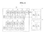
- FIG. 6 is a block diagram illustrating a semiconductor device according to exemplary embodiments of the present disclosure.
- a clock management unit 110 a in a semiconductor device 1 may include a first PLL controller 111 (also referred to as a first PLL controller circuit), a first clock MUX unit 112 (also referred to as a first clock MUX circuit), a first clock dividing unit 113 (also referred to as a first clock dividing circuit or a first clock dividing component), a first clock gating unit 114 (also referred to as a first clock gating circuit), a first channel management unit 115 (also referred to as a first channel management circuit), a second PLL controller 121 (also referred to as a second PLL controller circuit), a second clock MUX unit 122 (also referred to as a second clock MUX circuit), a second clock dividing unit 123 (also referred to as a second clock dividing circuit), and a second clock gating unit 124 (also referred to as a second clock gating circuit).
- a first PLL controller 111 also referred to as a first
- FIG. 6 illustrates an exemplary embodiment in which an operation of a second IP block 172 is dependent on an operation of a first IP block 171 .
- FIG. 6 illustrates an exemplary embodiment in which the second IP block 172 operates whenever the first IP block 171 operates.
- the second IP block 172 has the possibility to operate when the first IP block 171 operates.
- the first channel management unit 115 may communicate with the first clock gating unit 114 and/or the second clock gating unit 124 according to a full handshake method. For example, when the first IP block 171 transmits a clock request signal REQ to the first channel management unit 115 , the first channel management unit 115 may transmit the clock request signal REQ to the first clock gating unit 114 .
- the first PLL controller 111 , the first clock MUX unit 112 , the first clock dividing unit 113 , the first clock gating unit 114 , and the first channel management unit 115 may communicate with one another according to a full handshake method, and the clock request signal REQ can be transmitted from the first channel management unit 115 to the first PLL controller 111 at a time.
- the first clock MUX unit 112 may include a control circuit and a clock multiplexer circuit.
- the control circuit of the first clock MUX unit 112 may include an arbiter circuit, a multiplexer converter circuit, and an adapter circuit.
- Other MUX units described herein may include a similar configuration to the first clock MUX unit 112 .
- the clock acknowledgement signal ACK When the clock acknowledgement signal ACK is transmitted from the first PLL controller 111 , the clock acknowledgement signal ACK may be transmitted to the first clock gating unit 114 , the clock gating circuit may be deactivated according to a control of a control circuit included in the first clock gating unit 114 , and the first clock CLK 1 may be provided to the first IP block 171 .
- the first IP block 171 may deactivate the clock request signal REQ.
- the clock request signal REQ transmitted to the first clock gating unit 114 may be deactivated and clock gating may be performed according to a control of the control circuit included in the first clock gating unit 114 .
- the second IP block 172 Since an operation of the second IP block 172 is dependent on an operation of the first IP block 171 , the second IP block 172 cannot generate a clock request signal, and when the clock request signal REQ is activated in the first IP block 171 , the second clock CLK 2 may be provided to the second IP block 172 from the second clock gating unit 124 .
- the second PLL controller 121 , the second clock MUX unit 122 , the second clock dividing unit 123 , the second clock gating unit 124 , and the first channel management unit 115 may communicate with one another according to a full handshake method, and the clock request signal REQ can be transmitted from the first channel management unit 115 to the second PLL controller 121 at a time.
- the clock acknowledgement signal ACK When the clock acknowledgement signal ACK is transmitted from the second PLL controller 121 , the clock acknowledgement signal ACK may be transmitted to the second clock gating unit 124 , the clock gating circuit may be deactivated according to a control of a control circuit included in the second clock gating unit 124 , and the second clock CLK 2 may be provided to the second IP block 172 .
- the clock gating unit 114 (also referred to as a clock generating circuit), which includes a control circuit and a clock gating circuit, communicates with the channel management unit 115 (also referred to as a channel management circuit) according to a full handshake method and outputs a first clock to the IP block 171 .
- the clock gating unit 124 (also referred to as a clock generating circuit), which includes a control circuit and a clock gating circuit, communicates with the channel management circuit 115 according to a full handshake method and outputs a second clock different from the first clock to the IP block 172 .
- FIG. 7 is a block diagram illustrating a semiconductor device according to exemplary embodiments of the present disclosure.
- a clock management unit 110 b in a semiconductor device 2 may include the first PLL controller 111 , the first clock MUX unit 112 , the first clock dividing unit 113 , the first clock gating unit 114 , the first channel management unit 115 , a third clock gating unit 125 , and a second channel management unit 126 . According to exemplary embodiments, some of these components may be omitted or duplicated in the clock management unit 110 b.
- FIG. 7 illustrates an exemplary embodiment in which the second channel management unit 126 is used as a dummy unit.
- the second channel management unit 126 may control the clock request signal REQ according to a control of software stored in a separate special function register (SFR).
- SFR special function register
- the software stored in the SFR may determine whether the second IP block 172 needs a clock, and may control the clock request signal REQ according to a control of separate software.
- the first channel management unit 115 may communicate with the first clock gating unit 114 according to a full handshake method
- the second channel management unit 126 may communicate with the third clock gating unit 125 according to a full handshake method.
- the first channel management unit 115 may transmit the clock request signal REQ to the first clock gating unit 114 .
- the second IP block 172 does not directly communicate with the second channel management unit 126 .
- the first PLL controller 111 , the first clock MUX unit 112 , the first clock dividing unit 113 , the first clock gating unit 114 , and the first channel management unit 115 may communicate with one another according to a full handshake method, and the clock request signal REQ can be transmitted from the first channel management unit 115 to the first PLL controller 111 at a time.
- the clock acknowledgement signal ACK When the clock acknowledgement signal ACK is transmitted from the first PLL controller 111 , the clock acknowledgement signal ACK may be transmitted to the first clock gating unit 114 , the clock gating circuit included in the first clock gating unit 114 may be deactivated according to a control of the control circuit included in the first clock gating unit 114 , and the first clock CLK 1 may be provided to the first IP block 171 .
- the first PLL controller 111 , the first clock MUX unit 112 , the first clock dividing unit 113 , the third clock gating unit 125 , and the second channel management unit 126 may communicate with one another according to a full handshake method, and the clock request signal REQ can be transmitted from the second channel management unit 126 to the first PLL controller 111 at a time.
- the first clock dividing unit 113 may include a control circuit and a clock dividing circuit.
- the control circuit included in the first clock dividing unit 113 may include an arbiter circuit and an adapter circuit.
- the clock acknowledgement signal ACK When the clock acknowledgement signal ACK is transmitted from the first PLL controller 111 , the clock acknowledgement signal ACK may be transmitted to the third clock gating unit 125 , the clock gating circuit included in the third clock gating unit 125 may be deactivated according to a control of a control circuit included in the third clock gating unit 125 , and the second clock CLK 2 may be provided to the second IP block 172 .
- the first IP block 171 may deactivate the clock request signal REQ.
- the clock request signal REQ transmitted to the first clock gating unit 114 may be deactivated and clock gating may be performed according to a control of the control circuit included in the first clock gating unit 114 .
- the clock request signal REQ may be deactivated according to a control of the software included in the SFR, and clock gating may be performed according to the control of the control circuit included in the third clock gating unit 125 .
- FIG. 8 is a block diagram illustrating a semiconductor device according to exemplary embodiments of the present disclosure.
- a clock management unit 110 c in a semiconductor device 3 may include the first PLL controller 111 , the first clock MUX unit 112 , the first clock dividing unit 113 , the first clock gating unit 114 , the first channel management unit 115 , the third clock gating unit 125 , and a third channel management unit 127 . According to exemplary embodiments, some of these components may be omitted or duplicated in the clock management unit 110 c.
- FIG. 8 illustrates an exemplary embodiment in which an operation of the first IP block 171 and an operation of the second IP block 172 are independent of each other.
- the first IP block 171 operates regardless of whether the second IP block 172 operates and vice versa, and the first IP block 171 and the second IP block 172 may perform clock requesting independently of each other.
- the first channel management unit 115 may communicate with the first clock gating unit 114 according to a full handshake method
- the third channel management unit 127 may communicate with the third clock gating unit 125 according to a full handshake method.
- the first IP block 171 transmits the clock request signal REQ to the first channel management unit 115
- the first channel management unit 115 transmits the clock request signal REQ to the first clock gating unit 114
- the second IP block 172 may independently transmit the clock request signal REQ to the third channel management unit 127
- the third channel management unit 127 may transmit the clock request signal REQ to the third clock gating unit 125 .
- the first PLL controller 111 , the first clock MUX unit 112 , the first clock dividing unit 113 , the first clock gating unit 114 , and the first channel management unit 115 may communicate with one another according to a full handshake method, and the clock request signal REQ can be transmitted from the first channel management unit 115 to the first PLL controller 111 at a time.
- the clock acknowledgement signal ACK When the clock acknowledgement signal ACK is transmitted from the first PLL controller 111 , the clock acknowledgement signal ACK may be transmitted to the first clock gating unit 114 , the clock gating circuit may be deactivated according to a control of the control circuit included in the first clock gating unit 114 , and the first clock signal CLK 1 may be provided to the first IP block 171 .
- the first PLL controller 111 , the first clock MUX unit 112 , the first clock dividing unit 113 , the third clock gating unit 125 , and the third channel management unit 127 may communicate with one another according to a full handshake method, and the clock request signal REQ can be transmitted from the third channel management unit 127 to the first PLL controller 111 at a time.
- the clock acknowledgement signal ACK When the clock acknowledgement signal ACK is transmitted from the first PLL controller 111 , the clock acknowledgement signal ACK may be transmitted to the third clock gating unit 125 , the clock gating circuit included in the third clock gating unit 125 may be deactivated according to a control of the control circuit included in the third clock gating unit 125 , and the second clock CLK 2 may be provided to the second IP block 172 .
- the first IP block 171 may deactivate the clock request signal REQ.
- the clock request signal REQ transmitted to the first clock gating unit 114 may be deactivated and clock gating may be performed according to a control of the control circuit included in the first clock gating unit 114 .
- the second IP block 172 may deactivate the clock request signal REQ.
- the clock request signal REQ transmitted to the third clock gating unit 125 may be deactivated and clock gating may be performed according to a control of the control circuit included in the third clock gating unit 125 .
- the clock gating unit 114 (also referred to as a clock generating circuit), which includes a control circuit and a clock gating circuit, communicates with the channel management unit 115 (also referred to as a channel management circuit) according to a full handshake method.
- the clock gating unit 125 (also referred to as a clock generating circuit), which includes a control circuit and a clock gating circuit, communicates with the channel management unit 127 (also referred to as a channel management circuit) according to a full handshake method.
- the clock gating circuit 114 outputs a first clock to the IP block 171
- the clock gating circuit 125 outputs a second clock different from the first clock to the IP block 172 .
- FIG. 9A is a block diagram illustrating a semiconductor device according to exemplary embodiments of the present disclosure.
- FIG. 9B is a timing diagram illustrating an operation of the semiconductor device of FIG. 9A according to exemplary embodiments of the present disclosure.
- a clock management unit 110 d in a semiconductor device 4 may include the first PLL controller 111 , the first clock MUX unit 112 , the first clock dividing unit 113 , the first clock gating unit 114 , the first channel management unit 115 , and the third clock gating unit 125 . According to exemplary embodiments, some of these components may be omitted or duplicated in the clock management unit 110 d.
- FIGS. 9A and 9B illustrate an exemplary embodiment in which a channel management unit and clock gating units, which are its parents, are connected to one another in a 1:n relationship.
- FIGS. 9A and 9B illustrate an exemplary embodiment in which a plurality of clock gating units share one channel management unit among them during operation.
- an operation of the second IP block 172 is dependent on an operation of the first IP block 171 , and the second block 172 operates whenever the first IP block 171 operates.
- the second IP block 172 has the possibility to operate when the first IP block 171 operates.
- the first channel management unit 115 may communicate with the first clock gating unit 114 and/or the third clock gating unit 125 according to a full handshake method. For example, when the first IP block 171 transmits a clock request signal REQ to the first channel management unit 115 , the first channel management unit 115 may transmit the clock request signal REQ to the first clock gating unit 114 .
- the first PLL controller 111 , the first clock MUX unit 112 , the first clock dividing unit 113 , the first clock gating unit 114 , and the first channel management unit 115 may communicate with one another according to a full handshake method, and the clock request signal REQ can be transmitted from the first channel management unit 115 to the first PLL controller 111 at a time.
- the clock acknowledgement signal ACK When the clock acknowledgement signal ACK is transmitted from the first PLL controller 111 , the clock acknowledgement signal ACK may be transmitted to the first clock gating unit 114 , the clock gating circuit may be deactivated according to a control of the control circuit included in the first clock gating unit 114 , and the first clock CLK 1 may be provided to the first IP block 171 .
- the second IP block 172 Since an operation of the second IP block 172 is dependent on an operation of the first IP block 171 , the second IP block 172 cannot generate a clock request signal, and when the clock request signal REQ is activated in the first IP block 171 , the second clock CLK 2 may be provided to the second IP block 172 from the second clock gating unit 124 .
- the first PLL controller 111 , the first clock MUX unit 112 , the first clock dividing unit 113 , the third clock gating unit 125 , and the first channel management unit 115 may communicate with one another according to a full handshake method, and the clock request signal REQ can be transmitted from the first channel management unit 115 to the first PLL controller 111 at a time.
- the clock acknowledgement signal ACK When the clock acknowledgement signal ACK is transmitted from the first PLL controller 111 , the clock acknowledgement signal ACK may be transmitted to the third clock gating unit 125 , the clock gating circuit included in the third clock gating unit 125 may be deactivated according to a control of the control circuit included in the third clock gating unit 125 , and the second clock CLK 2 may be provided to the second IP block 172 .
- the first IP block 171 may deactivate the clock request signal REQ.
- the clock request signal REQ transmitted to the first clock gating unit 114 may be deactivated and clock gating may be performed according to a control of the control circuit included in the first clock gating unit 114 .
- the clock request signal REQ transmitted to the third clock gating unit 125 may also be deactivated and clock gating may be performed according to a control of the control circuit included in the third clock gating unit 125 .
- FIG. 10A is a block diagram illustrating a semiconductor device according to exemplary embodiments of the present disclosure.
- FIG. 10B is a timing diagram illustrating an operation of the semiconductor device of FIG. 10A according to exemplary embodiments of the present disclosure.
- a clock management unit 110 e in a semiconductor device 5 may include the first PLL controller 111 , the first clock MUX unit 112 , the first clock dividing unit 113 , the first clock gating unit 114 , the first channel management unit 115 , and a fourth channel management unit 128 . According to exemplary embodiments, some of these components may be omitted or duplicated in the clock management unit 110 e.
- FIGS. 10A and 10B illustrate an exemplary embodiment in which channel management units and a clock gating unit, which is its parent, are connected to one another in an n:1 relationship.
- FIGS. 10A and 10B illustrate an exemplary embodiment in which a plurality of channel management units are connected to one clock gating unit.
- a plurality of IP blocks may use one clock among them (e.g., a plurality of IP blocks may share one clock).
- the plurality of IP blocks may use the same clock, and when there are clock requests from the plurality of IP blocks, a control circuit included in the clock gating unit may perform an OR operation so as to determine whether a clock is needed.
- the first channel management unit 115 may communicate with the first clock gating unit 114 according to a full handshake method
- the fourth channel management unit 128 may communicate with the first clock gating unit 114 according to a full handshake method.
- the first clock gating unit 114 may perform an OR operation.
- the first PLL controller 111 , the first clock MUX unit 112 , the first clock dividing unit 113 , the first clock gating unit 114 , and the first channel management unit 115 may communicate with one another according to a full handshake method, and the clock request signal REQ can be transmitted from the first channel management unit 115 to the first PLL controller 111 at a time.
- the clock acknowledgement signal ACK When the clock acknowledgement signal ACK is transmitted from the first PLL controller 111 , the clock acknowledgement signal ACK may be transmitted to the first clock gating unit 114 , the clock gating circuit may be deactivated according to a control of the control circuit included in the first clock gating unit 114 , and the first clock CLK 1 may be provided to the first IP block 171 .
- the first IP block 171 may deactivate the clock request signal REQ.
- the clock request signal REQ transmitted to the first clock gating unit 114 may be deactivated.
- the control circuit included in the first clock gating unit 114 may perform an AND operation so as to determine whether to perform clock gating.
- the first PLL controller 111 , the first clock MUX unit 112 , the first clock dividing unit 113 , the first clock gating unit 114 , and the fourth channel management unit 128 may communicate with one another according to a full handshake method, and the clock request signal REQ can be transmitted from the fourth channel management unit 128 to the first PLL controller 111 at a time.
- the clock acknowledgement signal ACK When the clock acknowledgement signal ACK is transmitted from the first PLL controller 111 , the clock acknowledgement signal ACK may be transmitted to the first clock gating unit 114 , the clock gating circuit may be deactivated according to a control of the control circuit included in the first clock gating unit 114 , and the first clock CLK 1 may be provided to the second IP block 172 . That is, the clock provided to the first IP block 171 and the clock provided to the second IP block 172 may be the same.
- the clock gating unit 114 (also referred to as a clock generating circuit), which includes a control circuit and a clock gating circuit, communicates with the channel management unit 115 (also referred to as a channel management circuit) according to a full handshake method. Further, the channel management unit 128 (also referred to as a channel management circuit) communicates with the clock generating circuit 114 according to a full handshake method.
- the channel management circuit 115 transmits a first clock request signal to the clock generating circuit 114 , and the channel management circuit 128 transmits a second clock request signal to the clock generating circuit 114 .
- the clock generating circuit 114 outputs a clock when at least one of the first clock request signal or the second clock request signal is activated.
- FIG. 11 is a block diagram illustrating a semiconductor device according to exemplary embodiments of the present disclosure.
- a clock management unit 110 f in a semiconductor device 6 may include the first controller 111 , the first clock MUX unit 112 , the first clock dividing unit 113 , a first clock gating unit 114 a , the first channel management unit 115 , the third clock gating unit 125 , the second PLL controller 121 , the second clock MUX unit 122 , the second clock dividing unit 123 , the second clock gating unit 124 , and the second channel management unit 126 .
- some of these components may be omitted or duplicated in the clock management unit 110 f.
- FIG. 11 illustrates an exemplary embodiment in which channel management units and clock gating units, which are their parents, are connected to one another in an win relationship. That is, FIG. 11 illustrates an exemplary embodiment in which the 1:n relationship and the n:1 relationship, which are described above, are both applied.
- An operation of the clock management unit 110 f in the semiconductor device 6 according to exemplary embodiments of the present disclosure may be substantially the same as those described above.
- FIG. 12 is a block diagram illustrating a semiconductor device according to exemplary embodiments of the present disclosure.
- a clock management unit 110 g in a semiconductor device 7 may include the first PLL controller 111 , the first clock MUX unit 112 , the first clock dividing unit 113 , a first clock gating unit 114 b , the first channel management unit 115 , the second PLL controller 121 , the second clock MUX unit 122 , the second clock dividing unit 123 , the second clock gating unit 124 , the second channel management unit 126 , and a fifth channel management unit 131 .
- some of these components may be omitted or duplicated in the clock management unit 110 g.
- FIG. 12 illustrates an exemplary embodiment in which channel management units and clock gating units, which are their parents, are connected to one another in an n:m relationship. That is, FIG. 12 illustrates an exemplary embodiment in which the 1:n relationship and the n:1 relationship, which are described above, are both applied.
- An operation of the clock management unit 110 g in the semiconductor device 7 according to exemplary embodiments of the present disclosure may be substantially the same as those described above.
- FIG. 13 is a block diagram illustrating a semiconductor device according to exemplary embodiments of the present disclosure.
- a semiconductor device 700 may include a central processing unit 710 , a clock generator 720 , a clock management unit 730 , a RAM 740 , a ROM 750 , and a memory control unit 760 connected to one another through a system bus.
- the oscillator OSC may be disposed outside the semiconductor device 700 so as to provide an oscillation signal to the semiconductor device 700 .
- the semiconductor device 700 illustrated in FIG. 13 is merely exemplary, and that the present disclosure is not limited thereto.
- the semiconductor device 700 may include various other functional blocks, and the oscillator OSC may be provided within the semiconductor device 700 .
- the semiconductor device 700 shown in FIG. 13 may be provided as an application processor in a semiconductor system.
- the clock generator 720 may generate a reference clock signal CLK_IN having a reference frequency by using a signal from the oscillator OSC.
- the clock management unit 730 may receive the reference clock signal CLK_IN, generate an operating clock signal CLK_OUT having a predetermined frequency, and provide the generated operating clock signal CLK_OUT to each of the functional blocks.
- the clock management unit 730 may include one or more master clock controller and slave clock controller, and each of the clock controllers may generate the operating clock signal CLK_OUT by using the reference clock signal CLK_IN.
- the clock controllers in the clock management unit 730 may be connected through a channel so as to manage clock signals in terms of hardware. Further, the clock controllers in the clock management unit 730 may be connected to the functional blocks through a channel so as to perform clock requesting and acknowledging to the request in terms of hardware.
- the central processing unit 710 may process or execute code and/or data stored in the RAM 740 .
- the central processing unit 710 may process or execute the code and/or data in response to an operating clock output from the clock management unit 730 .
- the central processing unit 710 may be implemented as a multi-core processor.
- the multi-core processor may be one computing component having two or more independent substantial processors, and each of the processors may read and execute program instructions.
- the multi-core processor may drive a plurality of accelerators at substantially the same time.
- a data processing system including the multi-core processor may perform multi-acceleration.
- the RAM 740 may temporarily store, for example, program code, data, or instructions therein.
- program code and/or data stored in an internal or external memory may be temporarily stored in the RAM 740 according to a control of the central processing unit 710 or a booting code stored in the ROM 750 .
- the memory control unit 760 may be a block for interfacing with the internal or external memory, and the memory control unit 760 may control overall operation of the memory, and also control general data exchange between a host and the memory.
- FIG. 14 is a block diagram illustrating a semiconductor device according to exemplary embodiments of the present disclosure.
- FIG. 14 illustrates an exemplary embodiment in which a semiconductor device 800 includes a power management unit 810 for managing power supplied to functional blocks.
- the power management unit 810 may be designed to manage power used inside the semiconductor device 800 .
- the semiconductor device 800 may include the power management unit 810 and a plurality of functional blocks 821 and 822 .
- the functional blocks 821 and 822 may be classified as a master functional block 821 and a slave functional block 822 .
- To operate the master functional block 821 power is supplied to the master functional block 821 .
- power is supplied to one or more slave functional blocks 822 associated with the operation of the master functional block 821 .
- a master power controller 811 may communicate with each of slave power controllers 812 and 813 through a channel.
- the power management unit 810 may receive input power Power_in, and control the power so as to convert the power to be suitable for each of the functional blocks, and may generate output power Power_out. Further, the power management unit 810 may provide power or cut off power supplied to the master functional block 821 and the slave functional block 822 according to a power request Req.
- the master power controller 811 may receive the power request Req in terms of software on the basis of code processing of the central processing unit, or receive the power request Req in terms of hardware from the master functional block 821 . Further, the master functional block 821 may provide power on/off instruction Pwr On/Off to the slave power controllers 812 and 813 , and receive power acknowledgement Ack On/Off from the slave power controllers 812 and 813 .
- FIG. 15 is a block diagram illustrating an embodiment of a semiconductor system including a semiconductor device according to exemplary embodiments of the present disclosure.
- a semiconductor system 900 may include a system-on-chip (SoC) 901 , an antenna 910 , a radio frequency transceiver 920 , an input device 930 , and a display 940 .
- the radio frequency transceiver 920 may transmit or receive radio frequency signals through the antenna 910 .
- the radio frequency transceiver 920 may convert the radio frequency signals received through the antenna 910 into signals which can be processed by the SoC 901 .
- the SoC 901 may process the signal output from the radio frequency transceiver 920 , and transmit the processed signal to the display 940 . Further, the radio frequency transceiver 920 may convert the signal output from the SoC 901 into a radio frequency signal, and output the converted radio frequency signal to an external device through the antenna 910 .
- the input device 930 may enable a control signal for controlling an operation of the SoC 901 or data to be processed by the SoC 901 to be input, and may be implemented as, for example, a pointing device such as a touch pad and a computer mouse, as well as a keypad, or a keyboard.
- FIG. 16 is a block diagram illustrating an embodiment of a semiconductor system including a semiconductor device according to exemplary embodiments of the present disclosure.
- a memory system 1000 may be implemented as a data processing device such as a solid state drive (SSD).
- the memory system 1000 may include a plurality of memory devices 1500 , a memory controller 1200 capable of controlling a data processing operation of each of the plurality of memory devices 1500 , a volatile memory device 1300 such as DRAM, and an SoC 1100 for controlling storage of data transmitted/received between the memory controller 1200 and a host 1400 , into the volatile memory device 1300 .
- the SoC 1100 may be implemented according to the exemplary embodiments described above.
- Exemplary embodiments of the present disclosure provide a semiconductor device in which a connection relation between a channel management unit and an intellectual property (IP) block is defined in an SoC so as to enable various clock consumers to be applied to the semiconductor device.
- IP intellectual property
Landscapes
- Engineering & Computer Science (AREA)
- Theoretical Computer Science (AREA)
- Physics & Mathematics (AREA)
- General Engineering & Computer Science (AREA)
- General Physics & Mathematics (AREA)
- Information Transfer Systems (AREA)
- Semiconductor Integrated Circuits (AREA)
Abstract
A semiconductor device includes a first clock generating circuit including a first control circuit and a first clock gating circuit, a first channel management circuit which communicates with the first clock generating circuit according to a full handshake method, a second clock generating circuit including a second control circuit and a second clock gating circuit, and a second channel management circuit which communicates with the second clock generating circuit according to the full handshake method. The first clock gating circuit outputs a first clock, and the second clock gating circuit outputs a second clock different from the first clock.
Description
This application claims priority to and the benefit of U.S. Provisional Patent Application No. 62/286,895 filed on Jan. 25, 2016, U.S. Provisional Patent Application No. 62/286,860 filed on Jan. 25, 2016, Korean Patent Application No. 10-2017-0007002 filed on Jan. 16, 2017, and Korean Patent Application No. 10-2017-0010945 filed on Jan. 24, 2017, the disclosures of which are incorporated by reference herein in their entireties.
Exemplary embodiments of the present disclosure relate to a semiconductor device including a semiconductor circuit.
With the gradual convergence of computers, communications, broadcasts, etc., the demand for existing application specific integrated circuits (ASICs) and application specific standard products (ASSPs) is changing due to the demand for system-on-chips (SoCs). Further, the trend toward lighter, thinner, more compact and high-performance information technology (IT) devices is a factor accelerating the development of SoCs.
With the development of semiconductor processing technology, SoCs may be implemented into a form in which conventional multi-functional blocks such as, for example, intellectual property (IP) blocks, are integrated on a single chip.
As SoCs increase in integration density and size, and as the operating speed thereof is improved, low power consumption becomes an important factor, since high power consumption may raise the temperature of a chip, resulting in the SoC malfunctioning or the SoC being damaged.
According to an exemplary embodiment of the present disclosure, a semiconductor device includes a first clock generating circuit including a first control circuit and a first clock gating circuit, a first channel management circuit which communicates with the first clock generating circuit according to a full handshake method, a second clock generating circuit including a second control circuit and a second clock gating circuit, and a second channel management circuit which communicates with the second clock generating circuit according to the full handshake method. The first clock gating circuit outputs a first clock, and the second clock gating circuit outputs a second clock different from the first clock.
According to an exemplary embodiment of the present disclosure, a semiconductor device includes a first clock generating circuit including a first control circuit and a first clock gating circuit, a first channel management circuit which communicates with the first clock generating circuit according to a full handshake method, and a second clock generating circuit including a second control circuit and a second clock gating circuit. The second clock generating circuit communicates with the first channel management circuit according to the full handshake method. The first clock gating circuit outputs a first clock, and the second clock gating circuit outputs a second clock different from the first clock.
According to an exemplary embodiment of the present disclosure, a semiconductor device includes a first clock generating circuit including a first control circuit and a first clock gating circuit, a first channel management circuit which communicates with the first clock generating circuit according to a full handshake method, and a second channel management circuit which communicates with the first clock generating circuit according to the full handshake method. The first channel management circuit transmits a first clock request signal to the first clock generating circuit, and the second channel management circuit transmits a second clock request signal to the first clock generating circuit.
The above and other features of the present disclosure will become more apparent by describing in detail exemplary embodiments thereof with reference to the accompanying drawings, in which:
It will be understood that the terms “first,” “second,” “third,” etc. are used herein to distinguish one element from another, and the elements are not limited by these terms. Thus, a “first” element in an exemplary embodiment may be described as a “second” element in another exemplary embodiment.
Further, when two processes are described as being performed substantially simultaneously or at substantially the same time as each other, it is to be understood that the processes may be performed at exactly the same time or at about the same time as would be understood by a person having ordinary skill in the art.
Further, it will be understood that each of the units described herein may be implemented as and referred to as circuits (e.g., a clock MUX unit be implemented as a circuit and referred to as a clock MUX circuit, a clock gating unit may be implemented as a circuit and referred to as a clock gating circuit, a channel management unit may be implemented as a circuit and referred to as a channel management circuit, etc.).
Referring to FIG. 1 , the semiconductor device according to exemplary embodiments of the present disclosure may include an input/output pad 101, a clock management unit (CMU) 100, a power management unit (PMU) 300, and a logic block. The logic block may be implemented as, for example, at least one intellectual property (IP) block 200, 210 and 220. IP blocks may also be referred to herein as logic blocks.
The clock management unit 100 may generate operation clock signals. The operation clock signals may be provided respectively to first to third IP blocks 200, 210 and 220. For example, the clock management unit 100 may generate first, second and third clock signals CLK1, CLK2 and CLK3, and respectively provide these clock signals to first to third IP blocks 200, 210 and 220.
Each of the first, second and third IP blocks 200, 210 and 220 may be connected to a system bus. The first, second and third IP blocks 200, 210 and 220 may communicate with one another through the system bus. In exemplary embodiments of the present disclosure, each of the first, second and third IP blocks 200, 210 and 220 may include, for example, a processor, a graphic processor, a memory controller, an input/output interface block, etc.
The clock management unit 100 may provide the first clock signal CLK1 to the first IP block 200, the second clock signal CLK2 to the second IP block 210, and the third clock signal CLK3 to the third IP block 220.
One of the first, second and third IP blocks 200, 210 and 220 may transmit a clock request signal to the clock management unit 100 according to a full handshake method.
For example, the first IP block 200 may transmit a first clock request signal REQ1 to the clock management unit 100 according to a full handshake method. The clock management unit 100 may receive the first clock request signal REQ1, and transmit a first clock acknowledgement signal ACK1 to the first IP block 200. The clock management unit 100 may substantially simultaneously transmit the first clock signal CLK1 to the first IP block 200. Similarly, the second and third IP blocks 210 and 220 may respectively transmit a second and third clock request signal REQ2 and REQ3 to the clock management unit 100, and the clock management unit 100 may respectively transmit a second and third clock acknowledgment signal ACK2 and ACK3 to the second and third IP blocks 210 and 220.
In exemplary embodiments of the present disclosure, an interface between the clock management unit 100 and the first, second and third IP blocks 200, 210 and 220 may adopt a format of a full handshake method. In exemplary embodiments of the present disclosure, the interface may be implemented to comply with Q-channel interface or P-channel interface of ARM Holdings, Ltd., but the scope of the present disclosure is not limited thereto.
Clock gating is a technique for grouping a computer system into small functional blocks, acid turning off the power in a block which is not used. When using a computer, not all parts of a computer system will operate at all times. Thus, a block in a part(s) which is not used can be switched off to save power, and heat which might otherwise be generated from the block can be reduced.
The clock management unit 100 according to exemplary embodiments of the present disclosure may perform, sequentially from a rear end of the IP blocks, clock gating on the IP block which does not need an operation clock from among the first, second and third IP blocks 200, 210 and 220 such that clock gating is automatically performed without causing an error to an operation of the IP blocks. As a result, power consumption may be reduced.
The power management unit 300 may control power being supplied to the semiconductor device. For example, when the semiconductor device enters a standby mode, the power management unit 300 may turn off a power control circuit so as to cut off power being supplied to the semiconductor device. In this case, the power management unit 300 may continuously consume power, but the power being consumed by the power management unit 300 may be significantly smaller than the power being supplied in the whole of the semiconductor device. Thus, power consumption in the semiconductor device may be substantially reduced in a standby mode.
For example, the power management unit 300 may cut off the power being supplied to the clock management unit 100 when the semiconductor device is in a standby mode. This may occur when the first, second and third IP blocks 200, 210 and 220 do not make a clock request.
Referring to FIG. 2 , the clock management unit 100 may include clock components 120 a, 120 b, 120 c, 120 d, 120 e, 120 f and 120 g (also referred to as clock generating circuits), channel management (CMM) circuits 130 and 132, and a clock management unit (CM) controller 110. The clock components 120 a, 120 b, 120 c, 120 d, 120 e, 120 f and 120 g may generate clock signals to be provided to the IF blocks 200 and 210. The CM circuits 130 and 132 may be respectively disposed between the clock components 120 f and 120 g and the IP blocks 200 and 210 so as to provide a communication channel CH between the clock management unit 100 and the IP blocks 200 and 210. The CMU controller 110 may provide a clock signal to the IP blocks 200 and 210 using the clock components 120 a, 120 b, 120 c, 120 d, 120 e, 120 f and 120 g. As shown in FIG. 2 , in an exemplary embodiment, the clock component 120 b may receive a clock from the clock component 120 a (e.g., CLK1) or a clock from, for example, an external device (e.g., from another CMU other than the CMU 100) (e.g., CLK2).
In exemplary embodiments of the present disclosure, the communication channel CH provided by the CM circuits 130 and 132 may be implemented to accord to a low power interface (LPI), Q-channel interface or P-channel interface of ARM Holdings, Ltd., but the scope of the present disclosure is not limited thereto. For example, according to exemplary embodiments, the communication channel CH can be implemented as those which comply with a certain preset communication protocol depending on purposes of implementation.
The clock components 120 a, 120 b, 120 c, 120 d, 120 e, 120 f and 120 g may respectively include clock sources CSs 124 a, 124 b, 124 c, 124 d, 124 e, 124 f and 124 g, and clock control circuits CCs 122 a, 122 b, 122 c, 122 d, 122 e, 122 f and 122 g (also referred to as control circuits) for controlling the respective clock sources 124 a, 124 b, 124 c, 124 d, 124 e, 124 f and 124 g. The clock sources CSs 124 a, 124 b, 124 c, 124 d, 124 e, 124 f and 124 g may include, for example, a multiplexer (MUX) circuit, a clock dividing circuit, a short stop circuit, a clock gating circuit, etc.
The clock components 120 a, 120 b, 120 c, 120 d, 120 e, 120 f and 120 g may form a parent-child relationship among them. In the embodiment shown in FIG. 2 , the clock component 120 a may be a parent of the clock component 120 b, and the clock component 120 b may be a child of the clock component 120 a and a parent of the clock component 120 c. Further, the clock component 120 e may be a parent of the two clock components 120 f and 120 g, and the clock components 120 f and 120 g may be children of the clock component 120 e. In the exemplary embodiment shown in FIG. 2 , the clock component 120 a disposed most adjacent to a phase locked loop (PLL) may be a root clock component, and the clock components 120 f and 120 g disposed most adjacent to the IP blocks 200 and 210 may be leaf clock components. The above-described parent-child relationship may also be formed among the clock control circuits 122 a, 122 b, 122 c, 122 d, 122 e, 122 f and 122 g, and among the clock sources 124 a, 124 b, 124 c, 124 d, 124 e, 124 f and 124 g according to the parent-child relationship formed among the clock components 120 a, 120 b, 120 c, 120 d, 120 e, 120 f and 120 g.
The clock control circuits 122 a, 122 b, 122 c, 122 d, 122 e, 122 f and 122 g may transmit and receive clock requests REQs and acknowledgements ACKs between parents and children, and provide clock signals to the IP blocks 200 and 210.
For example, when the IP block 200 does not need a clock signal, for example, when the IP block 200 is entering a sleep state, the clock management unit 100 may stop providing a clock signal to the IP block 200.
For example, the CM circuit 130 may transmit a first signal indicating stoppage of the clock signal to the IP block 200 under the control of the clock management unit 100 or the CMU controller 110. The IP block 200 which has received the first signal may finish the work under processing, and then transmit a second signal to the CM circuit 130 indicating that the clock signal may be stopped. The CM circuit 130 may receive the second signal from the IP block 200, and then request the clock component 120 f, which is its parent, to stop providing the clock signal.
In one example, when the communication channel CH provided by the CM circuit 130 complies with Q-channel interface, the CM circuit 130 may transmit, to the IP block 200, a QREQn signal having a first logic value (for example, logic low, which will hereinafter be denoted by L), as a first signal. Subsequently, the CM circuit 130 may receive, from the IP block 200, a QACCEPTn signal having, for example, a first logic value, as a second signal, and then transmit a clock request REQ having, for example, a first logic value, to the clock component 120 f. In this case, the clock request REQ having a first logic value may mean “a request to stop clock provision”.
The clock control circuit 122 f which has received, from the CM circuit 130, the clock request REQ having a first logic value (e.g., the request to stop clock provision), may disable the clock source 124 f (e.g., a clock gating circuit) so as to stop provision of the clock signal. As a result, the IP block 200 may enter a sleep mode. During the process, the clock control circuit 122 f may provide an acknowledgement ACK having a first logic value to the CM circuit 130. The CM circuit 130, which has transmitted the request to stop clock provision having a first logic value and then received the acknowledgement ACK having a first logic value, does not ensure stoppage of clock provision from the clock source 124 f. However, the acknowledgement ACK indicates that the clock control circuit 122 f has recognized that the clock component 120 f, which is a parent of the CM circuit 130, does not need to provide a clock to the CM circuit 130 any longer.
The clock control circuit 122 f of the clock component 120 f may transmit a clock request REQ having a first logic value to the clock control circuit 122 e of the clock component 120 e, which is its parent. If the IP block 210 also does not need a clock signal, when, for example, the clock control circuit 122 e has received a request to stop clock provision from the clock control circuit 122 g, the clock control circuit 122 e may disable the clock source 124 e (e.g., a clock diving circuit) so as to stop providing a clock signal. Thus, the IP blocks 200 and 210 may enter a sleep mode.
This operation may be performed in a similar manner on the other clock control circuits 122 a, 122 b, 122 c and 122 d.
When the clock control circuit 122 f of the clock component 120 f transmits a clock request REQ having a first logic value to the clock control circuit 122 e of the clock component 120 e, which is its parent, but the IP block 210 is in a running state (e.g., is not entering a sleep state), the clock control circuit 122 e may not disable the clock source 124 e. When the IP block 210 does not need a clock signal any longer afterward, the clock control circuit 122 e may then disable the clock source 124 e and transmit a clock signal REQ having a first logic value to the clock control circuit 122 d, which is its parent. That is, the clock control circuit 122 e may disable the clock source 124 e only when the clock control circuit 122 e has received requests to stop clock provision from both the clock control circuits 122 f and 122 g, which are its children.
When the IP blocks 200 and 210 are in a sleep state, and all of the clock sources 124 a, 124 b, 124 c, 124 d, 124 e and 124 f are disabled and the IP block 200 enters a running state, the clock management unit 100 may restart providing a clock signal to the IP blocks 200 and 210.
The CM circuit 130 may transmit a clock request REQ having a second logic value (e.g., logic high, which will hereinafter be denoted by H) to the clock control circuit 122 f of the clock component 120 f, which is its parent, and wait for an acknowledgement ACK from the clock control circuit 122 f. In this case, the clock request REQ having a second logic value may mean “a request for clock provision”, and the acknowledgement ACK for the request for clock provision may mean that the clock source 124 f has restarted clock provision. The clock control circuit 122 f may not directly enable the clock source 124 f (e.g., a clock gating circuit), and may wait for provision of a clock signal from its parent.
The clock control circuit 122 f may then transmit a clock request REQ having a second logic value, that is, a request for clock provision, to the clock control circuit 122 e, which is its parent, and wait for an acknowledgement ACK from the clock control circuit 122 e. This operation may be performed in a similar manner on the clock control circuits 122 a, 122 b, 122 c and 122 d.
The clock control circuit 122 a, which is a root clock component having received a clock request REQ having a second logic value from the clock control circuit 122 b may disable the clock source 124 a (e.g., a multiplexer circuit), and transmit an acknowledgement ACK to the clock control circuit 122 b. When the clock sources 124 b, 124 c, 124 d, 124 e and 124 f are sequentially disabled by the method described above, the clock control circuit 122 e may then transmit an acknowledgement ACK to the clock control circuit 122 f notifying it that the clock source 124 e has restarted providing a clock. The clock control circuit 122 f which has received the acknowledgement ACK may then enable the clock source 124 f to provide a clock signal to the IP block 200, and provide an acknowledgement ACK to the CM circuit 130.
As described above, the clock control circuits 122 a, 122 b, 122 c, 122 d, 122 e, 122 f and 122 g may operate according to a full handshake method in which a parent and children transmit and receive a clock request REQ and an acknowledgement ACK therebetween. That is, according to exemplary embodiments of the present disclosure, a full handshake method refers to an operation in which a parent and child transmit and receive a clock request REQ and an acknowledgment request ACK therebetween. Thus, the clock control circuits 122 a, 122 b, 122 c, 122 d, 122 e, 122 f and 122 g may control the clock sources 124 a, 124 b, 124 c, 124 d, 124 e, 124 f and 124 g in terms of hardware so as to control the clock signals provided to the IP blocks 200 and 210.
The clock control circuits 122 a, 122 b, 122 c, 122 d, 122 e, 122 f and 122 g may operate autonomously so as to transmit a clock request REQ to their parents or control the clock sources 124 a, 124 b, 124 c, 124 d, 124 e, 124 f and 124 g, and operate under the control of the CMU controller 110. In exemplary embodiments of the present disclosure, the clock control circuits 122 a, 122 b, 122 c, 122 d, 122 e, 122 f and 122 g may include a finite state machine (FSM) for controlling each of the clock sources 124 a, 124 b, 124 c, 124 d, 124 e, 124 f and 124 g according to the clock request REQ transmitted and received between parents and children.
According to exemplary embodiments, the clock component 120 f may communicate with the channel management circuit 130 according to a full handshake method, and may output a first clock to the IP block 200. Further, the clock component 120 g may communicate with the channel management circuit 132 according to a full handshake method, and may output a second clock different from the first clock to the IP block 210.
Referring to FIG. 3 , the first IP block 200 may include a channel adapter 202 and an IP core 204. FIG. 3 illustrates the IP block 200 as an example. It is to be understood that the second and third IP blocks 210 and 220 may include substantially the same components.
The channel adapter 202 may communicate with the first CM circuit 130 according to a full handshake method. The channel adapter 202 may be, for example, a Q-channel adapter. The first IP block 200 may transmit the first clock request signal REQ1 and receive the first clock signal CLK1 through the channel adapter 202. Alternatively, the first IP block 200 may transmit the first clock request signal REQ1 and receive an acknowledgement ACK signal indicating an existence of a clock through the channel adapter 202, and receive the first clock signal CLK1 directly from the clock component controlled by the channel adapter 202.
The IP core 204 may include, for example, a processor, a graphic processor, a memory controller, an input/output interface block, etc.
Referring to FIG. 4 , the plurality of clock control circuits may operate using a handshake signal including a clock request signal REQ and an acknowledgement signal ACK (also referred to as a clock acknowledgement signal). The clock request signal REQ and the clock acknowledgement signal ACK may have, for example, the first logic value (for example, logic low) and the second logic value (for example, logic high), but the method for implementing the clock request signal REQ and the clock acknowledgement signal ACK is not limited thereto.
In exemplary embodiments of the present disclosure, a clock consumer may deliver information indicating that a clock is needed, to a clock provider, by transmitting a clock request signal REQ having, for example, a second logic value, to the clock provider. Alternatively, the clock consumer may deliver information indicating that a clock is not needed any longer, to the clock provider, by transmitting a clock request signal REQ having, for example, a first logic value to the clock provider.
The clock provider may transmit a clock acknowledgement signal ACK having, for example, a second logic value, to the clock consumer, indicating that a clock signal is being stably provided to the clock consumer from the clock provider. Alternatively, the clock provider may transmit a clock acknowledgement signal ACK having a first logic value to the clock consumer, indicating that the clock provider is not capable of notifying, to the clock consumer, whether a clock signal is being provided.
For example, the clock control circuit 122 b may transmit, from a position of the clock consumer, a clock request signal (PARENT_CLK_REQ) having, for example, a second logic value, to the clock control circuit 122 a, thereby transmitting information indicating that a clock is needed, to the clock control circuit 122 a, which is the clock provider. The clock component (that is, the clock provider) including the clock control circuit 122 a may provide a clock signal to the clock component (that is, the clock consumer) including the clock control circuit 122 b, and the clock control circuit 122 b may then receive a clock acknowledgement signal (PARENT_CLK_ACK) having, for example, a second logic value, from the clock control circuit 122 a.
The clock control circuit 122 b may receive, at a position of the clock provider, a clock request signal (CHILD_CLK_REQ) having, for example, a second logic value, from the clock control circuit 122 f, which indicates that the clock control circuit 122 f, which is the clock consumer, needs a clock. The clock component (that is, the clock provider) including the clock control circuit 122 b may then provide a clock signal to the clock component (that is, the clock consumer) including the clock control circuit 122 f, and the clock control circuit 122 b may then transmit, from a position of the clock provider, a clock acknowledgement signal (CHILD_CLK_ACK) having, for example, a second logic value, to the clock control circuit 122 f.
As another example, the clock control circuit 122 b may transmit, from a position of the clock consumer, a clock request signal (PARENT_CLK_REQ) having, for example, a first logic value, to the clock control circuit 122 a, thereby delivering information indicating that a clock is not needed any longer, to the clock control circuit 122 a, which is a clock provider. The clock control circuit 122 b may then receive a clock acknowledgement signal (PARENT_CLK_ACK) having, for example, a first logic value, from the clock control circuit 122 a, indicating that provision of a clock from the clock provider is not ensured (e.g., the clock control circuit 122 a (the clock provider) is not capable of notifying the clock control circuit 122 (the clock consumer) whether the requested clock signal is being provided).
The clock control circuit 122 b may receive, at a position of the clock provider, a clock request signal (CHILD_CLK_REQ) having, for example, a first logic value, from the clock control circuit 122 f, indicating that the clock control circuit 122 f, which is the clock consumer, does not need a clock any longer. The clock control circuit 122 b may then transmit a clock acknowledgement signal (CHILD_CLK_ACK) having, for example, a first logic value, to the clock control circuit 122 f, indicating that provision of a clock from the clock provider is not ensured.
A combinational path among the clock control circuits described above may include a path in which the clock control circuit 122 b transmits a clock request signal (PARENT_CLK_REQ) to the clock control circuit 122 a, which is its parent, and then the clock control circuit 122 b receives a clock acknowledgement signal (PARENT_CLK_ACK) from the clock control circuit 122 a, which is its parent, and a path in which the clock control circuit 122 b receives a clock request signal (CHILD_CLK_REQ) from the clock control circuit 122 f, which is its child, and then the clock control circuit 122 b transmits a clock acknowledgement signal (CHILD_CLK_ACK) to the clock control circuit 122 f, which is its child, but may not include a path in Which the clock control circuit 122 b receives the clock acknowledgement signal (PARENT_CLK_ACK) from the clock control circuit 122 a, which is its parent, and then transmits the clock request signal (PARENT_CLK_REQ) to the clock control circuit 122 a, which is its parent (shown as “X” in FIG. 4 ).
The clock request signal REQ and the clock acknowledgement signal ACK described above may be implemented according to a general full handshake method, and the clock provider and the clock consumer may belong to the same single clock domain or clock domains different from each other. When a clock provider and a clock consumer belong to a single clock domain, they operate in response to a same reference clock signal. When a clock provider and a clock consumer belong to different clock domains, they operate in response to different reference clock signals.
In exemplary embodiments of the present disclosure, a clock multiplexer circuit, a clock dividing circuit, a clock gating circuit, etc. connected to and communicating with the respective clock control circuits may use a clock domain different from those of the clock control circuits. That is, the clock frequency in a signal line transmitting a clock request signal and the clock frequency of an actually provided operating clock may be different from each other.
Referring to FIG. 5A , the transition of the clock request signal REQ to a second logic value at time T1 may indicate that the clock consumer transmits, to the clock provider, information indicating that a clock signal CLK is needed. The clock provider may provide a clock signal CLK to the clock consumer after time T1.
At time T2, the clock provider may transmit a clock acknowledgement signal ACK having a second logic value to the clock consumer, which may indicate that a clock signal CLK is being stably provided to the clock consumer from the clock provider (see section I).
At time T3, the transition of the clock request signal REQ to a first logic value may indicate that the clock consumer transmits, to the clock provider, information indicating that a clock signal CLK is not needed any longer. After time T3, the clock provider may stop providing the clock signal CLK to the clock consumer, or still continue providing the clock signal CLK.
At time T4, the clock provider may transmit, to the clock consumer, a clock acknowledgement signal ACK having a first logic value, which may indicate that the clock provider is not capable of notifying, to the clock consumer, whether a clock signal is being provided.
Thus, referring to FIG. 5A , section I is the only section in which the clock signal CLK is being stably provided from the clock provider to the clock consumer, and whether the clock signal CLK is being provided from the clock provider to the clock consumer is unknown in the other sections II.
Referring to both FIG. 5A and FIG. 5B , state S0 indicates a state before time T1 and a state after time T4, and state S1 indicates a state from time T1 to time T2. In addition, state S2 indicates a state from time T2 to time T3, and state S3 indicates a state from time T3 to time T4. A combination of the clock request signal REQ and the clock acknowledgement signal ACK may change in the order of state S0, state S1, state S2, state S3, and state S0 (see arrows in a solid line).
When a circuit is implemented such that the clock request signal REQ is transitioned to a second logic value and the clock acknowledgement signal ACK is substantially simultaneously transitioned to a second logic value at time T1, a combination of values of the clock request signal REQ and the clock acknowledgement signal ACK may be transitioned directly to state S2 from state S0. Similarly, when a circuit is implemented such that the clock request signal REQ is transitioned to a first logic value and the clock acknowledgement signal ACK is substantially simultaneously transitioned to a first logic value at time T3, a combination of values of the clock request signal REQ and the clock acknowledgement signal ACK may be transitioned directly to state S0 from state S2 (see arrows in dotted lines).
A full handshake method according to exemplary embodiments of the present disclosure will be described with reference to FIGS. 1, 2, and 4 .
The full handshake method is configured to enable the first IP block 200 to activate the first clock request signal REQ1 when the first IP block 200 needs a clock. For example, the first IP block 200 may turn the first clock request signal REQ1 to a high state.
The clock management unit 100 may activate the first clock acknowledgement signal ACK1 to the first clock request signal REQ1 in response to the activation of the first clock request signal REQ1. That is, the clock management unit 100 may turn the first clock acknowledgement signal ACK1 to a high state.
The clock management unit 100 may transmit the first clock signal CLK1 to the first IP block 200 prior to the activation of the first clock acknowledgement signal ACK1. Alternatively, the clock management unit 100 may transmit the first clock signal CLK1 to the first IP block 200 substantially simultaneously with the activation of the first clock acknowledgement signal ACK1.
When the first IP block 200 does not need a clock, the first IP block 200 may deactivate the first clock request signal REQ1. That is, the first IP block 200 may turn the first clock request signal REQ1 to a low state.
When the first clock request signal REQ1 is in a low state, the clock management unit 100 may turn the first clock acknowledgement signal ACK1 to a low state. In addition, the clock management unit 100 may substantially simultaneously deactivate the first clock signal CLK1.
The first IP block 200 can operate normally while the first clock acknowledgement signal ACK1 is in the activated state.
A full handshake method of the clock management unit 100 according to exemplary embodiments of the present disclosure will now be described with reference to FIGS. 1 and 2 . The description will be made under the assumption that the clock components 120 a, 120 b, 120 c, 120 d, 120 e and 120 f of FIG. 2 are respectively a phase locked loop (PLL) controller, a clock MUX unit, a first clock dividing unit, a short stop circuit, a second clock dividing unit, and a first clock gating unit. However, it is to be understood that this is merely an exemplary embodiment, and the scope of the present disclosure is not limited thereto.
Each of the PLL controller, the clock MUX unit, the first clock dividing unit, the short stop circuit, the second clock dividing unit, and the first clock gating unit may include the clock sources 124 a, 124 b, 124 c, 124 d, 124 e and 124 f.
For example, the PLL controller may include an oscillator OSC and a clock MUX circuit for taking, as an input, a PLL. The clock MUX unit may include a clock MUX circuit for taking, as an input, a plurality of clock signals. The first clock dividing unit may include a first clock dividing circuit. The short stop circuit may include a first clock gating circuit. The second clock dividing unit may include a second clock dividing circuit. The first clock gating unit may include a second clock gating circuit.
Further, the PLL controller may include the clock control circuit 122 a. The clock MUX unit may include the clock control circuit 122 b. The first clock dividing unit may include the clock control circuit 122 e. A short stop circuit 114 may include the clock control circuit 122 d. The second clock dividing unit may include the clock control circuit 122 e. The first clock gating unit may include the clock control circuit 122 f.
Each of the clock control circuits 122 a, 122 b, 122 c, 122 d, 122 e and 122 f may communicate according to a full handshake method. For example, each of the clock control circuits 122 a and 122 b may support a full handshake method between the PLL controller and the clock MUX unit.
Each of the clock control circuits 122 b and 122 c may support a full handshake method between the clock MUX unit and the first clock dividing unit.
Each of the clock control circuits 122 c and 122 d may support a full handshake method between the first clock dividing unit and the short stop circuit.
Each of the clock control circuits 122 d and 122 e may support a full handshake method between the short stop circuit and the second clock dividing unit.
Each of the clock control circuits 122 e and 122 f may support a full handshake method between the second clock dividing unit and the first clock gating unit.
Similarly, each of the clock control circuit 122 f and the CM circuit 130 may support a full handshake method between the first clock gating unit and the CM circuit 130.
According to exemplary embodiments of the present disclosure, a clock request signal may indicate that the corresponding IP block desires for the CMU 100 to provide it with a clock signal or desires for the CMU 100 to stop providing it with the clock signal. According to exemplary embodiments, in a full handshake method, the CMU 100 responds to a clock request signal with a clock acknowledgement signal indicating it is currently providing or is about to provide the requested clock signal, or it has stopped providing or is about to stop providing the requested clock signal, and the CMU 100 responds with a clock acknowledgement signal indicating only that it is acknowledging receipt of the clock request signal without providing information on the state of the clock signal. Thus, in exemplary embodiments, the full handshake method may refer to connected clock components (e.g., a parent clock component and a child clock component) exchanging a clock request signal and a clock acknowledgement signal therebetween.
The first IP block 200 may make a request for an operation clock to the clock management unit 100 according to a full handshake method. For example, the IP block 200 may activate a clock request signal when an operation clock is needed. That is, the first IP block 200 may transmit an activated clock request signal to the clock management unit 100 when an operation clock is needed.
The CM circuit 130 may receive the activated clock request signal. The CM circuit 130 may transmit the activated clock request signal to the first clock gating unit. The first clock gating unit may transmit the activated clock request signal to the second clock dividing unit. The second clock dividing unit may transmit the activated clock request signal to the short stop circuit. The short stop circuit may transmit the activated clock request signal to the first clock dividing unit. The first clock dividing unit may transmit the activated clock request signal to the clock MUX unit. The clock MUX unit may transmit the activated clock request signal to the PLL controller.
In exemplary embodiments of the present disclosure, each of the PLL controller, the clock MUX unit, the first clock dividing unit, the short stop circuit, the second clock dividing unit, the first clock gating unit, and the first CM circuit 130 may be implemented as a combinational circuit. Accordingly, the activated clock request signal can be transmitted from the first CM circuit to the PLL controller at a time.
The PLL controller may activate a clock acknowledgement signal with respect to the activated clock request signal. That is, the PLL controller may transmit, to the clock MUX unit, a clock acknowledgement signal in response to the activated clock request signal. At substantially the same time, the PLL controller may transmit a clock signal CLK to the clock MUX unit.
The clock MUX unit may transmit the activated clock acknowledgement signal to the first clock dividing unit. At substantially the same time, the clock MUX unit may transmit the clock signal CLK to the first clock dividing unit.
The first clock dividing unit may transmit the activated clock acknowledgement signal to the short stop circuit. At substantially the same time, the first clock dividing unit may transmit the clock signal CLK to the short stop circuit.
The short stop circuit may transmit the activated clock acknowledgement signal to the second clock dividing unit. At substantially the same time, the short stop circuit may transmit the clock signal CLK to the second clock dividing unit.
The second clock dividing unit may transmit the activated clock acknowledgement signal to the first gating unit. At substantially the same time, the second clock dividing unit may transmit the clock signal CLK to the first clock gating unit.
The first clock gating unit may transmit the activated clock acknowledgement signal to the first CM circuit 130. At substantially the same time, the first clock gating unit may provide the clock signal CLK to the first IP block 200.
Thus, as can be seen, in an exemplary embodiment, the clock acknowledgement signal can be transmitted from the PLL controller to the first CM circuit at a time.
The first IP block 200 may deactivate the clock request signal when a clock is not needed. That is, the first IP block 200 may transmit the deactivated clock request signal to the clock management unit 100 when a clock is not needed.
The CM circuit 130 may receive the deactivated clock request signal. The CM circuit 130 may transmit the deactivated clock request signal to the first clock gating unit. The first clock gating unit may transmit the deactivated clock request signal to the second clock dividing unit. The second clock dividing unit may transmit the deactivated clock request signal to the short stop circuit. The short stop circuit may transmit the deactivated clock request signal to the first clock dividing unit. The first clock dividing unit may transmit the deactivated clock request signal to the clock MUX unit. The clock MUX unit may transmit the deactivated clock request signal to the PLL controller.
Each of the PLL controller, the clock MUX unit, the first clock dividing unit, the short stop circuit, the second clock dividing unit, the first clock gating unit, and the first CM circuit 130 may be implemented as a combinational circuit. Accordingly, the deactivated clock request signal can be transmitted from the first CM circuit to the PLL controller at a time.
The PLL controller may deactivate a clock acknowledgement signal with respect to the deactivated clock request signal. That is, the PLL controller may transmit, to the clock MUX unit, the deactivated clock acknowledgement signal. At substantially the same time, the PLL controller may deactivate a clock signal CLK, and may still transmit the clock signal CLK to the clock MUX unit.
The clock MUX unit may transmit the deactivated clock acknowledgement signal to the first clock dividing unit. At substantially the same time, the clock MUX unit may deactivate the clock signal CLK, and may still transmit the clock signal CLK to the first clock dividing unit.
The first clock dividing unit may transmit the deactivated clock acknowledgement signal to the short stop circuit. At substantially the same time, the first clock dividing unit may deactivate the clock signal CLK, and may still transmit the clock signal CLK to the short stop circuit.
The short stop circuit may transmit the deactivated clock acknowledgement signal to the second clock dividing unit. At substantially the same time, the short stop circuit may deactivate the clock signal CLK, and may still transmit the clock signal CLK to the second clock dividing unit.
The second clock dividing unit may transmit the deactivated clock acknowledgement signal to the first clock gating unit. At substantially the same time, the second clock dividing unit may deactivate the clock signal CLK, and may still transmit the clock signal CLK to the first clock gating unit.
The first clock gating unit may transmit the deactivated clock acknowledgement signal to the CM circuit 130. At substantially the same time, the first clock gating unit may deactivate the clock signal CLK.
Similarly, the clock acknowledgement signal can be transmitted from the PLL controller to the first CM circuit 130 at a time.
Referring to FIG. 6 , a clock management unit 110 a in a semiconductor device 1 according to exemplary embodiments of the present disclosure may include a first PLL controller 111 (also referred to as a first PLL controller circuit), a first clock MUX unit 112 (also referred to as a first clock MUX circuit), a first clock dividing unit 113 (also referred to as a first clock dividing circuit or a first clock dividing component), a first clock gating unit 114 (also referred to as a first clock gating circuit), a first channel management unit 115 (also referred to as a first channel management circuit), a second PLL controller 121 (also referred to as a second PLL controller circuit), a second clock MUX unit 122 (also referred to as a second clock MUX circuit), a second clock dividing unit 123 (also referred to as a second clock dividing circuit), and a second clock gating unit 124 (also referred to as a second clock gating circuit). According to exemplary embodiments, some of these components may be omitted or duplicated in the clock management unit 110 a.
The first channel management unit 115 may communicate with the first clock gating unit 114 and/or the second clock gating unit 124 according to a full handshake method. For example, when the first IP block 171 transmits a clock request signal REQ to the first channel management unit 115, the first channel management unit 115 may transmit the clock request signal REQ to the first clock gating unit 114.
The first PLL controller 111, the first clock MUX unit 112, the first clock dividing unit 113, the first clock gating unit 114, and the first channel management unit 115 may communicate with one another according to a full handshake method, and the clock request signal REQ can be transmitted from the first channel management unit 115 to the first PLL controller 111 at a time. The first clock MUX unit 112 may include a control circuit and a clock multiplexer circuit. The control circuit of the first clock MUX unit 112 may include an arbiter circuit, a multiplexer converter circuit, and an adapter circuit. Other MUX units described herein may include a similar configuration to the first clock MUX unit 112.
When the clock acknowledgement signal ACK is transmitted from the first PLL controller 111, the clock acknowledgement signal ACK may be transmitted to the first clock gating unit 114, the clock gating circuit may be deactivated according to a control of a control circuit included in the first clock gating unit 114, and the first clock CLK1 may be provided to the first IP block 171.
When the first IP block 171 does not need the first clock CLK1, the first IP block 171 may deactivate the clock request signal REQ. Thus, the clock request signal REQ transmitted to the first clock gating unit 114 may be deactivated and clock gating may be performed according to a control of the control circuit included in the first clock gating unit 114.
Since an operation of the second IP block 172 is dependent on an operation of the first IP block 171, the second IP block 172 cannot generate a clock request signal, and when the clock request signal REQ is activated in the first IP block 171, the second clock CLK2 may be provided to the second IP block 172 from the second clock gating unit 124.
The second PLL controller 121, the second clock MUX unit 122, the second clock dividing unit 123, the second clock gating unit 124, and the first channel management unit 115 may communicate with one another according to a full handshake method, and the clock request signal REQ can be transmitted from the first channel management unit 115 to the second PLL controller 121 at a time.
When the clock acknowledgement signal ACK is transmitted from the second PLL controller 121, the clock acknowledgement signal ACK may be transmitted to the second clock gating unit 124, the clock gating circuit may be deactivated according to a control of a control circuit included in the second clock gating unit 124, and the second clock CLK2 may be provided to the second IP block 172.
Referring to FIG. 6 , according to an exemplary embodiment, the clock gating unit 114 (also referred to as a clock generating circuit), which includes a control circuit and a clock gating circuit, communicates with the channel management unit 115 (also referred to as a channel management circuit) according to a full handshake method and outputs a first clock to the IP block 171. Further, the clock gating unit 124 (also referred to as a clock generating circuit), which includes a control circuit and a clock gating circuit, communicates with the channel management circuit 115 according to a full handshake method and outputs a second clock different from the first clock to the IP block 172.
Referring to FIG. 7 , a clock management unit 110 b in a semiconductor device 2 according to exemplary embodiments of the present disclosure may include the first PLL controller 111, the first clock MUX unit 112, the first clock dividing unit 113, the first clock gating unit 114, the first channel management unit 115, a third clock gating unit 125, and a second channel management unit 126. According to exemplary embodiments, some of these components may be omitted or duplicated in the clock management unit 110 b.
The software stored in the SFR may determine whether the second IP block 172 needs a clock, and may control the clock request signal REQ according to a control of separate software.
The first channel management unit 115 may communicate with the first clock gating unit 114 according to a full handshake method, and the second channel management unit 126 may communicate with the third clock gating unit 125 according to a full handshake method.
For example, when the clock request signal REQ is transmitted to the first channel management unit 115 by the first IP block 171, the first channel management unit 115 may transmit the clock request signal REQ to the first clock gating unit 114. However, as described above, the second IP block 172 does not directly communicate with the second channel management unit 126.
The first PLL controller 111, the first clock MUX unit 112, the first clock dividing unit 113, the first clock gating unit 114, and the first channel management unit 115 may communicate with one another according to a full handshake method, and the clock request signal REQ can be transmitted from the first channel management unit 115 to the first PLL controller 111 at a time.
When the clock acknowledgement signal ACK is transmitted from the first PLL controller 111, the clock acknowledgement signal ACK may be transmitted to the first clock gating unit 114, the clock gating circuit included in the first clock gating unit 114 may be deactivated according to a control of the control circuit included in the first clock gating unit 114, and the first clock CLK1 may be provided to the first IP block 171.
Further, the first PLL controller 111, the first clock MUX unit 112, the first clock dividing unit 113, the third clock gating unit 125, and the second channel management unit 126 may communicate with one another according to a full handshake method, and the clock request signal REQ can be transmitted from the second channel management unit 126 to the first PLL controller 111 at a time. The first clock dividing unit 113 may include a control circuit and a clock dividing circuit. The control circuit included in the first clock dividing unit 113 may include an arbiter circuit and an adapter circuit.
When the clock acknowledgement signal ACK is transmitted from the first PLL controller 111, the clock acknowledgement signal ACK may be transmitted to the third clock gating unit 125, the clock gating circuit included in the third clock gating unit 125 may be deactivated according to a control of a control circuit included in the third clock gating unit 125, and the second clock CLK2 may be provided to the second IP block 172.
When the first IP block 171 does not need the first clock CLK1, the first IP block 171 may deactivate the clock request signal REQ. Thus, the clock request signal REQ transmitted to the first clock gating unit 114 may be deactivated and clock gating may be performed according to a control of the control circuit included in the first clock gating unit 114.
When the second IP block 172 does not need the second clock CLK2, the clock request signal REQ may be deactivated according to a control of the software included in the SFR, and clock gating may be performed according to the control of the control circuit included in the third clock gating unit 125.
Referring to FIG. 8 , a clock management unit 110 c in a semiconductor device 3 according to exemplary embodiments of the present disclosure may include the first PLL controller 111, the first clock MUX unit 112, the first clock dividing unit 113, the first clock gating unit 114, the first channel management unit 115, the third clock gating unit 125, and a third channel management unit 127. According to exemplary embodiments, some of these components may be omitted or duplicated in the clock management unit 110 c.
The first channel management unit 115 may communicate with the first clock gating unit 114 according to a full handshake method, and the third channel management unit 127 may communicate with the third clock gating unit 125 according to a full handshake method.
For example, when the first IP block 171 transmits the clock request signal REQ to the first channel management unit 115, the first channel management unit 115 transmits the clock request signal REQ to the first clock gating unit 114. Further, the second IP block 172 may independently transmit the clock request signal REQ to the third channel management unit 127, and the third channel management unit 127 may transmit the clock request signal REQ to the third clock gating unit 125.
The first PLL controller 111, the first clock MUX unit 112, the first clock dividing unit 113, the first clock gating unit 114, and the first channel management unit 115 may communicate with one another according to a full handshake method, and the clock request signal REQ can be transmitted from the first channel management unit 115 to the first PLL controller 111 at a time.
When the clock acknowledgement signal ACK is transmitted from the first PLL controller 111, the clock acknowledgement signal ACK may be transmitted to the first clock gating unit 114, the clock gating circuit may be deactivated according to a control of the control circuit included in the first clock gating unit 114, and the first clock signal CLK1 may be provided to the first IP block 171.
Further, the first PLL controller 111, the first clock MUX unit 112, the first clock dividing unit 113, the third clock gating unit 125, and the third channel management unit 127 may communicate with one another according to a full handshake method, and the clock request signal REQ can be transmitted from the third channel management unit 127 to the first PLL controller 111 at a time.
When the clock acknowledgement signal ACK is transmitted from the first PLL controller 111, the clock acknowledgement signal ACK may be transmitted to the third clock gating unit 125, the clock gating circuit included in the third clock gating unit 125 may be deactivated according to a control of the control circuit included in the third clock gating unit 125, and the second clock CLK2 may be provided to the second IP block 172.
When the first IP block 171 does not need the first clock CLK1, the first IP block 171 may deactivate the clock request signal REQ. Thus, the clock request signal REQ transmitted to the first clock gating unit 114 may be deactivated and clock gating may be performed according to a control of the control circuit included in the first clock gating unit 114.
When the second IP block 172 does not need the second clock CLK2, the second IP block 172 may deactivate the clock request signal REQ. Thus, the clock request signal REQ transmitted to the third clock gating unit 125 may be deactivated and clock gating may be performed according to a control of the control circuit included in the third clock gating unit 125.
Referring to FIG. 8 , according to an exemplary embodiment, the clock gating unit 114 (also referred to as a clock generating circuit), which includes a control circuit and a clock gating circuit, communicates with the channel management unit 115 (also referred to as a channel management circuit) according to a full handshake method. Further, the clock gating unit 125 (also referred to as a clock generating circuit), which includes a control circuit and a clock gating circuit, communicates with the channel management unit 127 (also referred to as a channel management circuit) according to a full handshake method. The clock gating circuit 114 outputs a first clock to the IP block 171, and the clock gating circuit 125 outputs a second clock different from the first clock to the IP block 172.
Referring to FIGS. 9A and 9B , a clock management unit 110 d in a semiconductor device 4 according to exemplary embodiments of the present disclosure may include the first PLL controller 111, the first clock MUX unit 112, the first clock dividing unit 113, the first clock gating unit 114, the first channel management unit 115, and the third clock gating unit 125. According to exemplary embodiments, some of these components may be omitted or duplicated in the clock management unit 110 d.
According to this configuration, an operation of the second IP block 172 is dependent on an operation of the first IP block 171, and the second block 172 operates whenever the first IP block 171 operates. Thus, according to exemplary embodiments, the second IP block 172 has the possibility to operate when the first IP block 171 operates.
The first channel management unit 115 may communicate with the first clock gating unit 114 and/or the third clock gating unit 125 according to a full handshake method. For example, when the first IP block 171 transmits a clock request signal REQ to the first channel management unit 115, the first channel management unit 115 may transmit the clock request signal REQ to the first clock gating unit 114.
The first PLL controller 111, the first clock MUX unit 112, the first clock dividing unit 113, the first clock gating unit 114, and the first channel management unit 115 may communicate with one another according to a full handshake method, and the clock request signal REQ can be transmitted from the first channel management unit 115 to the first PLL controller 111 at a time.
When the clock acknowledgement signal ACK is transmitted from the first PLL controller 111, the clock acknowledgement signal ACK may be transmitted to the first clock gating unit 114, the clock gating circuit may be deactivated according to a control of the control circuit included in the first clock gating unit 114, and the first clock CLK1 may be provided to the first IP block 171.
Since an operation of the second IP block 172 is dependent on an operation of the first IP block 171, the second IP block 172 cannot generate a clock request signal, and when the clock request signal REQ is activated in the first IP block 171, the second clock CLK2 may be provided to the second IP block 172 from the second clock gating unit 124.
The first PLL controller 111, the first clock MUX unit 112, the first clock dividing unit 113, the third clock gating unit 125, and the first channel management unit 115 may communicate with one another according to a full handshake method, and the clock request signal REQ can be transmitted from the first channel management unit 115 to the first PLL controller 111 at a time.
When the clock acknowledgement signal ACK is transmitted from the first PLL controller 111, the clock acknowledgement signal ACK may be transmitted to the third clock gating unit 125, the clock gating circuit included in the third clock gating unit 125 may be deactivated according to a control of the control circuit included in the third clock gating unit 125, and the second clock CLK2 may be provided to the second IP block 172.
When the first IP block 171 does not need the first clock CLK1, the first IP block 171 may deactivate the clock request signal REQ. Thus, the clock request signal REQ transmitted to the first clock gating unit 114 may be deactivated and clock gating may be performed according to a control of the control circuit included in the first clock gating unit 114. In this case, the clock request signal REQ transmitted to the third clock gating unit 125 may also be deactivated and clock gating may be performed according to a control of the control circuit included in the third clock gating unit 125.
Referring to FIGS. 10A and 10B , a clock management unit 110 e in a semiconductor device 5 according to exemplary embodiments of the present disclosure may include the first PLL controller 111, the first clock MUX unit 112, the first clock dividing unit 113, the first clock gating unit 114, the first channel management unit 115, and a fourth channel management unit 128. According to exemplary embodiments, some of these components may be omitted or duplicated in the clock management unit 110 e.
According to this configuration, a plurality of IP blocks may use one clock among them (e.g., a plurality of IP blocks may share one clock). For example, the plurality of IP blocks may use the same clock, and when there are clock requests from the plurality of IP blocks, a control circuit included in the clock gating unit may perform an OR operation so as to determine whether a clock is needed.
The first channel management unit 115 may communicate with the first clock gating unit 114 according to a full handshake method, and the fourth channel management unit 128 may communicate with the first clock gating unit 114 according to a full handshake method. For example, when the first IP block 171 transmits the clock request signal REQ to the first channel management unit 115, or when the second IP block 172 transmits the clock request signal REQ to the fourth channel management unit 128, the first clock gating unit 114 may perform an OR operation.
The first PLL controller 111, the first clock MUX unit 112, the first clock dividing unit 113, the first clock gating unit 114, and the first channel management unit 115 may communicate with one another according to a full handshake method, and the clock request signal REQ can be transmitted from the first channel management unit 115 to the first PLL controller 111 at a time.
When the clock acknowledgement signal ACK is transmitted from the first PLL controller 111, the clock acknowledgement signal ACK may be transmitted to the first clock gating unit 114, the clock gating circuit may be deactivated according to a control of the control circuit included in the first clock gating unit 114, and the first clock CLK1 may be provided to the first IP block 171.
When the first IP block 171 does not need the first clock CLK1, the first IP block 171 may deactivate the clock request signal REQ. As a result, the clock request signal REQ transmitted to the first clock gating unit 114 may be deactivated. In this case, the control circuit included in the first clock gating unit 114 may perform an AND operation so as to determine whether to perform clock gating.
The first PLL controller 111, the first clock MUX unit 112, the first clock dividing unit 113, the first clock gating unit 114, and the fourth channel management unit 128 may communicate with one another according to a full handshake method, and the clock request signal REQ can be transmitted from the fourth channel management unit 128 to the first PLL controller 111 at a time.
When the clock acknowledgement signal ACK is transmitted from the first PLL controller 111, the clock acknowledgement signal ACK may be transmitted to the first clock gating unit 114, the clock gating circuit may be deactivated according to a control of the control circuit included in the first clock gating unit 114, and the first clock CLK1 may be provided to the second IP block 172. That is, the clock provided to the first IP block 171 and the clock provided to the second IP block 172 may be the same.
According to an exemplary embodiment, referring to FIG. 10A , the clock gating unit 114 (also referred to as a clock generating circuit), which includes a control circuit and a clock gating circuit, communicates with the channel management unit 115 (also referred to as a channel management circuit) according to a full handshake method. Further, the channel management unit 128 (also referred to as a channel management circuit) communicates with the clock generating circuit 114 according to a full handshake method. The channel management circuit 115 transmits a first clock request signal to the clock generating circuit 114, and the channel management circuit 128 transmits a second clock request signal to the clock generating circuit 114. The clock generating circuit 114 outputs a clock when at least one of the first clock request signal or the second clock request signal is activated.
Referring to FIG. 11 , a clock management unit 110 f in a semiconductor device 6 according to exemplary embodiments of the present disclosure may include the first controller 111, the first clock MUX unit 112, the first clock dividing unit 113, a first clock gating unit 114 a, the first channel management unit 115, the third clock gating unit 125, the second PLL controller 121, the second clock MUX unit 122, the second clock dividing unit 123, the second clock gating unit 124, and the second channel management unit 126. According to exemplary embodiments, some of these components may be omitted or duplicated in the clock management unit 110 f.
An operation of the clock management unit 110 f in the semiconductor device 6 according to exemplary embodiments of the present disclosure may be substantially the same as those described above.
Referring to FIG. 12 , a clock management unit 110 g in a semiconductor device 7 according to exemplary embodiments of the present disclosure may include the first PLL controller 111, the first clock MUX unit 112, the first clock dividing unit 113, a first clock gating unit 114 b, the first channel management unit 115, the second PLL controller 121, the second clock MUX unit 122, the second clock dividing unit 123, the second clock gating unit 124, the second channel management unit 126, and a fifth channel management unit 131. According to exemplary embodiments, some of these components may be omitted or duplicated in the clock management unit 110 g.
An operation of the clock management unit 110 g in the semiconductor device 7 according to exemplary embodiments of the present disclosure may be substantially the same as those described above.
Referring to FIG. 13 , a semiconductor device 700 may include a central processing unit 710, a clock generator 720, a clock management unit 730, a RAM 740, a ROM 750, and a memory control unit 760 connected to one another through a system bus. The oscillator OSC may be disposed outside the semiconductor device 700 so as to provide an oscillation signal to the semiconductor device 700. It is to be understood that the semiconductor device 700 illustrated in FIG. 13 is merely exemplary, and that the present disclosure is not limited thereto. For example, in exemplary embodiments, the semiconductor device 700 may include various other functional blocks, and the oscillator OSC may be provided within the semiconductor device 700. The semiconductor device 700 shown in FIG. 13 may be provided as an application processor in a semiconductor system.
The clock generator 720 may generate a reference clock signal CLK_IN having a reference frequency by using a signal from the oscillator OSC. The clock management unit 730 may receive the reference clock signal CLK_IN, generate an operating clock signal CLK_OUT having a predetermined frequency, and provide the generated operating clock signal CLK_OUT to each of the functional blocks. The clock management unit 730 may include one or more master clock controller and slave clock controller, and each of the clock controllers may generate the operating clock signal CLK_OUT by using the reference clock signal CLK_IN.
Further, the clock controllers in the clock management unit 730 may be connected through a channel so as to manage clock signals in terms of hardware. Further, the clock controllers in the clock management unit 730 may be connected to the functional blocks through a channel so as to perform clock requesting and acknowledging to the request in terms of hardware.
The central processing unit 710 may process or execute code and/or data stored in the RAM 740. For example, the central processing unit 710 may process or execute the code and/or data in response to an operating clock output from the clock management unit 730. The central processing unit 710 may be implemented as a multi-core processor. The multi-core processor may be one computing component having two or more independent substantial processors, and each of the processors may read and execute program instructions. The multi-core processor may drive a plurality of accelerators at substantially the same time. Thus, a data processing system including the multi-core processor may perform multi-acceleration.
The RAM 740 may temporarily store, for example, program code, data, or instructions therein. For example, program code and/or data stored in an internal or external memory may be temporarily stored in the RAM 740 according to a control of the central processing unit 710 or a booting code stored in the ROM 750. The memory control unit 760 may be a block for interfacing with the internal or external memory, and the memory control unit 760 may control overall operation of the memory, and also control general data exchange between a host and the memory.
The semiconductor device 800 may include the power management unit 810 and a plurality of functional blocks 821 and 822. The functional blocks 821 and 822 may be classified as a master functional block 821 and a slave functional block 822. To operate the master functional block 821, power is supplied to the master functional block 821. In addition, power is supplied to one or more slave functional blocks 822 associated with the operation of the master functional block 821.
A master power controller 811 may communicate with each of slave power controllers 812 and 813 through a channel. The power management unit 810 may receive input power Power_in, and control the power so as to convert the power to be suitable for each of the functional blocks, and may generate output power Power_out. Further, the power management unit 810 may provide power or cut off power supplied to the master functional block 821 and the slave functional block 822 according to a power request Req.
The master power controller 811 may receive the power request Req in terms of software on the basis of code processing of the central processing unit, or receive the power request Req in terms of hardware from the master functional block 821. Further, the master functional block 821 may provide power on/off instruction Pwr On/Off to the slave power controllers 812 and 813, and receive power acknowledgement Ack On/Off from the slave power controllers 812 and 813.
Referring to FIG. 15 , according to exemplary embodiments, a semiconductor system 900 may include a system-on-chip (SoC) 901, an antenna 910, a radio frequency transceiver 920, an input device 930, and a display 940. The radio frequency transceiver 920 may transmit or receive radio frequency signals through the antenna 910. For example, the radio frequency transceiver 920 may convert the radio frequency signals received through the antenna 910 into signals which can be processed by the SoC 901.
Therefore, the SoC 901 may process the signal output from the radio frequency transceiver 920, and transmit the processed signal to the display 940. Further, the radio frequency transceiver 920 may convert the signal output from the SoC 901 into a radio frequency signal, and output the converted radio frequency signal to an external device through the antenna 910. The input device 930 may enable a control signal for controlling an operation of the SoC 901 or data to be processed by the SoC 901 to be input, and may be implemented as, for example, a pointing device such as a touch pad and a computer mouse, as well as a keypad, or a keyboard.
Referring to FIG. 16 , a memory system 1000 may be implemented as a data processing device such as a solid state drive (SSD). The memory system 1000 may include a plurality of memory devices 1500, a memory controller 1200 capable of controlling a data processing operation of each of the plurality of memory devices 1500, a volatile memory device 1300 such as DRAM, and an SoC 1100 for controlling storage of data transmitted/received between the memory controller 1200 and a host 1400, into the volatile memory device 1300. The SoC 1100 may be implemented according to the exemplary embodiments described above.
Exemplary embodiments of the present disclosure provide a semiconductor device in which a connection relation between a channel management unit and an intellectual property (IP) block is defined in an SoC so as to enable various clock consumers to be applied to the semiconductor device.
While the present disclosure has been particularly illustrated and described with reference to the exemplary embodiments thereof it will be understood by those of ordinary skill in the art that various changes in form and detail may be made therein without departing from the spirit and scope of the present disclosure as defined by the following claims.
Claims (15)
1. A semiconductor device, comprising:
a first clock generating circuit including a first control circuit and a first clock gating circuit;
a first channel management circuit which communicates with the first clock generating circuit according to a full handshake method;
a second clock generating circuit including a second control circuit and a second clock gating circuit; and
a second channel management circuit which communicates with the second clock generating circuit according to the full handshake method,
wherein the first clock gating circuit outputs a first clock, and the second clock gating circuit outputs a second clock different from the first clock,
wherein the first channel management circuit transmits a second clock request signal to the first clock generating circuit in response to a first clock request signal, and the first clock generating circuit transmits a first clock acknowledgement signal to the first channel management circuit in response to the second clock request signal,
wherein the second channel management circuit transmits a fourth clock request signal to the second clock generating circuit in response to a third clock request signal, and the second clock generating circuit transmits a second clock acknowledgement signal to the second channel management circuit in response to the fourth clock request signal.
2. The semiconductor device of claim 1 , wherein the first control circuit deactivates the first clock gating circuit when the second clock request signal is activated, and the second control circuit deactivates the second clock gating circuit when the fourth clock request signal is activated.
3. The semiconductor device of claim 1 , further comprising:
a first logic block which communicates with the first channel management circuit, and a second logic block which communicates with the second channel management circuit.
4. The semiconductor device of claim 3 , wherein the first channel management circuit and the first logic block communicate using the full handshake method.
5. The semiconductor device of claim 3 , wherein the first logic block is an intellectual property (IP) block, and the IP block activates the first clock request signal when the first clock is needed by the IP block.
6. The semiconductor device of claim 5 , wherein the first clock generating circuit provides the first clock to the IP block in response to the first clock request signal.
7. The semiconductor device of claim 6 , wherein the IP block deactivates the first clock request signal when the first clock is not needed by the IP block.
8. The semiconductor device of claim 1 , wherein the first clock generating circuit and the first channel management circuit communicate using a single clock domain.
9. The semiconductor device of claim 8 , wherein the first control circuit and the first clock gating circuit use different clock domains.
10. A semiconductor device, comprising:
a first clock generating circuit including a first control circuit and a first clock gating circuit;
a first channel management circuit which communicates with the first clock generating circuit according to a full handshake method; and
a second clock generating circuit including a second control circuit and a second clock gating circuit,
wherein the second clock generating circuit communicates with the first channel management circuit according to the full handshake method, and
the first clock gating circuit outputs a first clock, and the second clock gating circuit outputs a second clock different from the first clock,
wherein the first channel management circuit transmits a first clock request signal to the first clock generating circuit, and a second clock request signal to the second clock generating circuit,
wherein the first clock generating circuit transmits a first clock acknowledgement signal to the first channel management circuit in response to the first clock request signal,
wherein the second clock generating circuit transmits a second clock acknowledgement signal to the first channel management circuit in response to the second clock request signal.
11. The semiconductor device of claim 10 , wherein the first control circuit deactivates the first clock gating circuit when the first clock request signal is activated, and the second control circuit deactivates the second clock gating circuit when the second clock request signal is activated.
12. A semiconductor device, comprising:
a first clock generating circuit including a first control circuit and a first clock gating circuit;
a first channel management circuit which communicates with the first clock generating circuit according to a full handshake method; and
a second channel management circuit which communicates with the first clock generating circuit according to the full handshake method,
wherein the first channel management circuit transmits a first clock request signal to the first clock generating circuit, and the second channel management circuit transmits a second clock request signal to the first clock generating circuit,
wherein the first clock generating circuit transmits a first clock acknowledgment signal to the first channel management circuit in response to the first clock request signal, and transmits a second clock acknowledgment signal to the second channel management circuit in response to the second clock request signal.
13. The semiconductor device of claim 12 , wherein the first clock generating circuit outputs a first clock when at least one of the first clock request signal or the second clock request signal is activated.
14. The semiconductor device of claim 13 , further comprising:
a first logic block which communicates with the first channel management circuit using the full handshake method; and
a second logic block which communicates with the second channel management circuit using the full handshake method.
15. The semiconductor device of claim 14 , wherein the first clock generating circuit provides the first clock to at least one of the first logic block or the second logic block.
Priority Applications (4)
| Application Number | Priority Date | Filing Date | Title |
|---|---|---|---|
| US15/415,041 US10248155B2 (en) | 2016-01-25 | 2017-01-25 | Semiconductor device including clock generating circuit and channel management circuit |
| DE102017110788.6A DE102017110788A1 (en) | 2016-01-25 | 2017-05-18 | Semiconductor device |
| CN201710600073.8A CN108319326B (en) | 2016-01-25 | 2017-07-21 | Semiconductor device with a plurality of semiconductor chips |
| TW106124821A TWI740988B (en) | 2016-01-25 | 2017-07-25 | Semiconductor device |
Applications Claiming Priority (7)
| Application Number | Priority Date | Filing Date | Title |
|---|---|---|---|
| US201662286860P | 2016-01-25 | 2016-01-25 | |
| US201662286895P | 2016-01-25 | 2016-01-25 | |
| KR10-2017-0007002 | 2017-01-16 | ||
| KR1020170007002A KR102550422B1 (en) | 2016-01-25 | 2017-01-16 | Semiconductor device |
| KR10-2017-0010945 | 2017-01-24 | ||
| KR1020170010945A KR102467172B1 (en) | 2016-01-25 | 2017-01-24 | Semiconductor device |
| US15/415,041 US10248155B2 (en) | 2016-01-25 | 2017-01-25 | Semiconductor device including clock generating circuit and channel management circuit |
Publications (2)
| Publication Number | Publication Date |
|---|---|
| US20170212549A1 US20170212549A1 (en) | 2017-07-27 |
| US10248155B2 true US10248155B2 (en) | 2019-04-02 |
Family
ID=59360506
Family Applications (1)
| Application Number | Title | Priority Date | Filing Date |
|---|---|---|---|
| US15/415,041 Active 2037-04-09 US10248155B2 (en) | 2016-01-25 | 2017-01-25 | Semiconductor device including clock generating circuit and channel management circuit |
Country Status (1)
| Country | Link |
|---|---|
| US (1) | US10248155B2 (en) |
Cited By (1)
| Publication number | Priority date | Publication date | Assignee | Title |
|---|---|---|---|---|
| US11592861B2 (en) | 2020-08-12 | 2023-02-28 | Samsung Electronics Co., Ltd. | Semiconductor device |
Families Citing this family (1)
| Publication number | Priority date | Publication date | Assignee | Title |
|---|---|---|---|---|
| US11867744B2 (en) * | 2020-10-20 | 2024-01-09 | Nvidia Corporation | Techniques for isolating interfaces while testing semiconductor devices |
Citations (70)
| Publication number | Priority date | Publication date | Assignee | Title |
|---|---|---|---|---|
| US5373293A (en) | 1991-04-30 | 1994-12-13 | Kabushiki Kaisha Toshiba | Mixed analog/digital mixed integrated circuit having a digital clock inhibit |
| US5600839A (en) | 1993-10-01 | 1997-02-04 | Advanced Micro Devices, Inc. | System and method for controlling assertion of a peripheral bus clock signal through a slave device |
| US5655127A (en) | 1994-02-04 | 1997-08-05 | Intel Corporation | Method and apparatus for control of power consumption in a computer system |
| US5661751A (en) | 1994-02-02 | 1997-08-26 | Advanced Micro Devices | System and technique for power management of a universal asynchronous receiver/transmitter by automatic clock gating |
| US5793993A (en) | 1995-01-26 | 1998-08-11 | General Magic, Inc. | Method for transmitting bus commands and data over two wires of a serial bus |
| JPH11143570A (en) | 1997-11-11 | 1999-05-28 | Kawasaki Steel Corp | Clock stop signal generation circuit for lsi |
| US5978930A (en) | 1996-10-11 | 1999-11-02 | Nec Corporation | Clock signal control system for stopping and activating a clock signal |
| US6021501A (en) | 1995-05-26 | 2000-02-01 | National Semiconductor Corporation | Clock enable/disable circuit of power management system |
| US6437617B2 (en) | 1998-02-27 | 2002-08-20 | Nec Corporation | Method of controlling a clock signal and circuit for controlling a clock signal |
| US20020152407A1 (en) | 2000-11-03 | 2002-10-17 | Stmicroelectronics S.R.I. | Power down protocol for integrated circuits |
| US20030117176A1 (en) | 2001-08-29 | 2003-06-26 | Jean-Louis Tardieux | Generic serial port architecture and system |
| US6654898B1 (en) | 1999-07-15 | 2003-11-25 | Apple Computer, Inc. | Stable clock generation internal to a functional integrated circuit chip |
| US20040153678A1 (en) * | 2003-02-05 | 2004-08-05 | Infineon Technologies North America Corp. | Microprocessor idle mode management system |
| US6822481B1 (en) | 2003-06-12 | 2004-11-23 | Agilent Technologies, Inc. | Method and apparatus for clock gating clock trees to reduce power dissipation |
| US20040243874A1 (en) | 2003-05-30 | 2004-12-02 | Byers Charles Calvin | Programmable clock management component reconfiguration upon receipt of one or more control signals to be able to process one or more frequency signals |
| US6915438B2 (en) | 2003-04-04 | 2005-07-05 | Arraycomm, Inc | Distributed power management method for monitoring control/status signal of sub-modules to manage power of sub-modules by activating clock signal during operation of sub-modules |
| US6927604B2 (en) * | 2003-08-21 | 2005-08-09 | International Business Machines Corporation | Clock signal selector circuit with reduced probability of erroneous output due to metastability |
| US20050232218A1 (en) * | 2004-04-19 | 2005-10-20 | Broadcom Corporation | Low-power operation of systems requiring low-latency and high-throughput |
| KR20060064146A (en) | 2004-12-08 | 2006-06-13 | 어보브반도체 주식회사 | Low power micro controller |
| US20060161797A1 (en) | 2003-01-24 | 2006-07-20 | Eckhard Grass | Asynchronous wrapper for a globally asynchronous, locally synchronous (gals) circuit |
| US7111183B1 (en) | 2002-10-10 | 2006-09-19 | Lattice Semiconductor Corporation | Expansion method for complex power-sequencing applications |
| US20060248367A1 (en) | 2005-04-29 | 2006-11-02 | Fischer Timothy C | Count calibration for synchronous data transfer between clock domains |
| US7142478B2 (en) | 2004-03-19 | 2006-11-28 | Infineon Technologies Ag | Clock stop detector |
| US7162556B2 (en) | 2004-02-20 | 2007-01-09 | Oki Electric Industry Co., Ltd. | Matrix type bus connection system and power reduction method therefor |
| US7174467B1 (en) | 2001-07-18 | 2007-02-06 | Advanced Micro Devices, Inc. | Message based power management in a multi-processor system |
| JP2007065756A (en) | 2005-08-29 | 2007-03-15 | Nec Corp | Clock control circuit, clock control method, semiconductor integrated circuit device, and electronic apparatus |
| US7245161B2 (en) * | 2005-09-15 | 2007-07-17 | International Business Machines Corporation | Apparatus and method for verifying glitch-free operation of a multiplexer |
| JP2008097594A (en) | 2006-09-14 | 2008-04-24 | Yaskawa Electric Corp | Low power consumption system and method of low power consumption for use in this system |
| US20080178024A1 (en) | 2006-02-15 | 2008-07-24 | Oki Electric Industry Co., Ltd. | Multilayered bus system |
| KR100852885B1 (en) | 2006-08-08 | 2008-08-19 | 엠텍비젼 주식회사 | Circuit and method for controlling current consumed therein in power-down mode, and i2c interface circuit |
| US7443218B2 (en) | 2005-06-29 | 2008-10-28 | Renesas Technology Corp. | Semiconductor integrated circuit with pulsed clock data latch |
| US20080301604A1 (en) | 2007-05-30 | 2008-12-04 | Alexander Itskovich | Apparatus for and method of estimating the quality of clock gating solutions for integrated circuit design |
| US20090150706A1 (en) | 2007-12-11 | 2009-06-11 | Myeong-Hoon Oh | Wrapper circuit for globally asynchronous locally synchronous system and method for operating the same |
| JP2010021793A (en) | 2008-07-10 | 2010-01-28 | Toshiba Corp | Semiconductor integrated circuit device and power consumption control method |
| US7694042B2 (en) | 2005-11-03 | 2010-04-06 | Samsung Electronics Co., Ltd. | Instantaneous data-driven clock-gating device and hard-wired streaming processing system including the same |
| US7797561B1 (en) | 2006-12-21 | 2010-09-14 | Nvidia Corporation | Automatic functional block level clock-gating |
| US7813908B2 (en) | 2007-04-27 | 2010-10-12 | Freescale Semiconductor, Inc. | Clock control module simulator and method thereof |
| US20110050300A1 (en) | 2007-09-27 | 2011-03-03 | Peter Klapproth | Clock Generator |
| US7971086B2 (en) | 2007-02-06 | 2011-06-28 | D. S. P. Group Ltd. | Integrated waking/while-awake power management system with breaking distance timer for high wake-up latency portion of hardware |
| US20110202788A1 (en) | 2010-02-12 | 2011-08-18 | Blue Wonder Communications Gmbh | Method and device for clock gate controlling |
| US8086975B2 (en) | 2008-04-10 | 2011-12-27 | University Of Southern California | Power aware asynchronous circuits |
| US8132144B2 (en) | 2009-06-17 | 2012-03-06 | Oracle America, Inc. | Automatic clock-gating insertion and propagation technique |
| US8140925B2 (en) | 2007-06-26 | 2012-03-20 | International Business Machines Corporation | Method and apparatus to debug an integrated circuit chip via synchronous clock stop and scan |
| US20120131370A1 (en) | 2008-09-25 | 2012-05-24 | Ren Wang | Conserving power in a computer system |
| US8289048B2 (en) | 2010-04-28 | 2012-10-16 | Intel Corporation | State transitioning clock gating |
| US8291244B2 (en) | 2006-07-28 | 2012-10-16 | Arm Limited | Power management in a data processing device having masters and slaves |
| US8375239B2 (en) | 2010-02-26 | 2013-02-12 | Renesas Electronics Corporation | Clock control signal generation circuit, clock selector, and data processing device |
| US20130055004A1 (en) * | 2011-08-31 | 2013-02-28 | Kleanthes Koniaris | Hardware-based automatic clock gating |
| US20130124895A1 (en) | 2011-11-14 | 2013-05-16 | Texas Instruments Incorporated | Microprocessor based power management system architecture |
| US20130173951A1 (en) * | 2011-12-30 | 2013-07-04 | Gabriel Vogel | Controlling communication of a clock signal to a peripheral |
| US8533648B2 (en) | 2010-05-13 | 2013-09-10 | Oracle International Corporation | Automatic clock-gating propagation technique |
| US8572418B2 (en) | 2009-03-12 | 2013-10-29 | Qualcomm Incorporated | Moving clock gating cell closer to clock source based on enable signal propagation time to clocked storage element |
| US8656196B2 (en) | 2010-04-07 | 2014-02-18 | Apple Inc. | Hardware automatic performance state transitions in system on processor sleep and wake events |
| US20140082396A1 (en) | 2012-09-14 | 2014-03-20 | Oracle International Corporation | Method and apparatus for distributed generation of multiple configurable ratioed clock domains within a high speed domain |
| US20140089697A1 (en) | 2012-09-27 | 2014-03-27 | Soo Yong KIM | System-on-chip with capability for controlling power supply according to data transaction and method of operating the same |
| US8826047B1 (en) * | 2009-03-02 | 2014-09-02 | Marvell International Ltd. | Self governing power management architecture that allows independent management of devices based on clock signals and a plurality of control signals written to control registers |
| US20140266333A1 (en) * | 2013-03-12 | 2014-09-18 | Sebastien Jouin | Generating clock on demand |
| US8898502B2 (en) | 2011-07-05 | 2014-11-25 | Psion Inc. | Clock domain crossing interface |
| US8924612B2 (en) | 2012-04-04 | 2014-12-30 | Arm Limited | Apparatus and method for providing a bidirectional communications link between a master device and a slave device |
| JP5678849B2 (en) | 2011-09-14 | 2015-03-04 | 株式会社デンソー | Communication system and transceiver |
| US8996906B1 (en) * | 2010-05-13 | 2015-03-31 | Tabula, Inc. | Clock management block |
| US20150200669A1 (en) | 2012-09-19 | 2015-07-16 | Qualcomm Incorporated | Clock gating circuit for reducing dynamic power |
| US9152598B2 (en) | 2012-11-28 | 2015-10-06 | Atmel Corporation | Connecting multiple slave devices to a single master controller in bus system |
| US9172377B2 (en) | 2011-01-10 | 2015-10-27 | Taiwan Semiconductor Manufacturing Company, Ltd. | Clock-tree transformation in high-speed ASIC implementation |
| US20150373313A1 (en) | 2012-07-23 | 2015-12-24 | Seiko Epson Corporation | Projector and control method therefor |
| US20160094337A1 (en) | 2014-09-30 | 2016-03-31 | Youn-Sik CHOI | System-on-chip to support full handshake and mobile device having the same |
| KR20160038671A (en) | 2014-09-30 | 2016-04-07 | 삼성전자주식회사 | System-on-chip to support full handshake and mobile device having the same |
| US20160116934A1 (en) | 2014-10-23 | 2016-04-28 | Samsung Electronics Co., Ltd. | Clock circuit for generating clock signal and semiconductor integrated circuit device including the same |
| US20160350259A1 (en) | 2015-05-26 | 2016-12-01 | Samsung Electronics Co., Ltd. | System on chip including clock management unit and method of operating the system on chip |
| US9766648B2 (en) | 2013-07-16 | 2017-09-19 | Ford Global Technologies, Llc | Controller system coordinated using a timing signal and method of controller coordination using a timing signal |
-
2017
- 2017-01-25 US US15/415,041 patent/US10248155B2/en active Active
Patent Citations (74)
| Publication number | Priority date | Publication date | Assignee | Title |
|---|---|---|---|---|
| US5373293A (en) | 1991-04-30 | 1994-12-13 | Kabushiki Kaisha Toshiba | Mixed analog/digital mixed integrated circuit having a digital clock inhibit |
| US5600839A (en) | 1993-10-01 | 1997-02-04 | Advanced Micro Devices, Inc. | System and method for controlling assertion of a peripheral bus clock signal through a slave device |
| US5661751A (en) | 1994-02-02 | 1997-08-26 | Advanced Micro Devices | System and technique for power management of a universal asynchronous receiver/transmitter by automatic clock gating |
| US5655127A (en) | 1994-02-04 | 1997-08-05 | Intel Corporation | Method and apparatus for control of power consumption in a computer system |
| US5793993A (en) | 1995-01-26 | 1998-08-11 | General Magic, Inc. | Method for transmitting bus commands and data over two wires of a serial bus |
| US6021501A (en) | 1995-05-26 | 2000-02-01 | National Semiconductor Corporation | Clock enable/disable circuit of power management system |
| US5978930A (en) | 1996-10-11 | 1999-11-02 | Nec Corporation | Clock signal control system for stopping and activating a clock signal |
| JPH11143570A (en) | 1997-11-11 | 1999-05-28 | Kawasaki Steel Corp | Clock stop signal generation circuit for lsi |
| US6437617B2 (en) | 1998-02-27 | 2002-08-20 | Nec Corporation | Method of controlling a clock signal and circuit for controlling a clock signal |
| US6654898B1 (en) | 1999-07-15 | 2003-11-25 | Apple Computer, Inc. | Stable clock generation internal to a functional integrated circuit chip |
| US20020152407A1 (en) | 2000-11-03 | 2002-10-17 | Stmicroelectronics S.R.I. | Power down protocol for integrated circuits |
| US7174467B1 (en) | 2001-07-18 | 2007-02-06 | Advanced Micro Devices, Inc. | Message based power management in a multi-processor system |
| US20030117176A1 (en) | 2001-08-29 | 2003-06-26 | Jean-Louis Tardieux | Generic serial port architecture and system |
| US6889331B2 (en) | 2001-08-29 | 2005-05-03 | Analog Devices, Inc. | Dynamic voltage control method and apparatus |
| US7111183B1 (en) | 2002-10-10 | 2006-09-19 | Lattice Semiconductor Corporation | Expansion method for complex power-sequencing applications |
| US20060161797A1 (en) | 2003-01-24 | 2006-07-20 | Eckhard Grass | Asynchronous wrapper for a globally asynchronous, locally synchronous (gals) circuit |
| US20040153678A1 (en) * | 2003-02-05 | 2004-08-05 | Infineon Technologies North America Corp. | Microprocessor idle mode management system |
| US6915438B2 (en) | 2003-04-04 | 2005-07-05 | Arraycomm, Inc | Distributed power management method for monitoring control/status signal of sub-modules to manage power of sub-modules by activating clock signal during operation of sub-modules |
| US20040243874A1 (en) | 2003-05-30 | 2004-12-02 | Byers Charles Calvin | Programmable clock management component reconfiguration upon receipt of one or more control signals to be able to process one or more frequency signals |
| US6822481B1 (en) | 2003-06-12 | 2004-11-23 | Agilent Technologies, Inc. | Method and apparatus for clock gating clock trees to reduce power dissipation |
| US6927604B2 (en) * | 2003-08-21 | 2005-08-09 | International Business Machines Corporation | Clock signal selector circuit with reduced probability of erroneous output due to metastability |
| US7162556B2 (en) | 2004-02-20 | 2007-01-09 | Oki Electric Industry Co., Ltd. | Matrix type bus connection system and power reduction method therefor |
| US7142478B2 (en) | 2004-03-19 | 2006-11-28 | Infineon Technologies Ag | Clock stop detector |
| US20050232218A1 (en) * | 2004-04-19 | 2005-10-20 | Broadcom Corporation | Low-power operation of systems requiring low-latency and high-throughput |
| KR20060064146A (en) | 2004-12-08 | 2006-06-13 | 어보브반도체 주식회사 | Low power micro controller |
| US20060248367A1 (en) | 2005-04-29 | 2006-11-02 | Fischer Timothy C | Count calibration for synchronous data transfer between clock domains |
| US7443218B2 (en) | 2005-06-29 | 2008-10-28 | Renesas Technology Corp. | Semiconductor integrated circuit with pulsed clock data latch |
| KR101184182B1 (en) | 2005-06-29 | 2012-09-18 | 르네사스 일렉트로닉스 가부시키가이샤 | A semiconductor integrated circuit device |
| JP2007065756A (en) | 2005-08-29 | 2007-03-15 | Nec Corp | Clock control circuit, clock control method, semiconductor integrated circuit device, and electronic apparatus |
| US7245161B2 (en) * | 2005-09-15 | 2007-07-17 | International Business Machines Corporation | Apparatus and method for verifying glitch-free operation of a multiplexer |
| US7694042B2 (en) | 2005-11-03 | 2010-04-06 | Samsung Electronics Co., Ltd. | Instantaneous data-driven clock-gating device and hard-wired streaming processing system including the same |
| US20080178024A1 (en) | 2006-02-15 | 2008-07-24 | Oki Electric Industry Co., Ltd. | Multilayered bus system |
| US8291244B2 (en) | 2006-07-28 | 2012-10-16 | Arm Limited | Power management in a data processing device having masters and slaves |
| KR100852885B1 (en) | 2006-08-08 | 2008-08-19 | 엠텍비젼 주식회사 | Circuit and method for controlling current consumed therein in power-down mode, and i2c interface circuit |
| JP2008097594A (en) | 2006-09-14 | 2008-04-24 | Yaskawa Electric Corp | Low power consumption system and method of low power consumption for use in this system |
| US7797561B1 (en) | 2006-12-21 | 2010-09-14 | Nvidia Corporation | Automatic functional block level clock-gating |
| US7971086B2 (en) | 2007-02-06 | 2011-06-28 | D. S. P. Group Ltd. | Integrated waking/while-awake power management system with breaking distance timer for high wake-up latency portion of hardware |
| US7813908B2 (en) | 2007-04-27 | 2010-10-12 | Freescale Semiconductor, Inc. | Clock control module simulator and method thereof |
| US20080301604A1 (en) | 2007-05-30 | 2008-12-04 | Alexander Itskovich | Apparatus for and method of estimating the quality of clock gating solutions for integrated circuit design |
| US8140925B2 (en) | 2007-06-26 | 2012-03-20 | International Business Machines Corporation | Method and apparatus to debug an integrated circuit chip via synchronous clock stop and scan |
| US20110050300A1 (en) | 2007-09-27 | 2011-03-03 | Peter Klapproth | Clock Generator |
| US20090150706A1 (en) | 2007-12-11 | 2009-06-11 | Myeong-Hoon Oh | Wrapper circuit for globally asynchronous locally synchronous system and method for operating the same |
| US8086975B2 (en) | 2008-04-10 | 2011-12-27 | University Of Southern California | Power aware asynchronous circuits |
| JP2010021793A (en) | 2008-07-10 | 2010-01-28 | Toshiba Corp | Semiconductor integrated circuit device and power consumption control method |
| US20120131370A1 (en) | 2008-09-25 | 2012-05-24 | Ren Wang | Conserving power in a computer system |
| US8826047B1 (en) * | 2009-03-02 | 2014-09-02 | Marvell International Ltd. | Self governing power management architecture that allows independent management of devices based on clock signals and a plurality of control signals written to control registers |
| US8572418B2 (en) | 2009-03-12 | 2013-10-29 | Qualcomm Incorporated | Moving clock gating cell closer to clock source based on enable signal propagation time to clocked storage element |
| US8132144B2 (en) | 2009-06-17 | 2012-03-06 | Oracle America, Inc. | Automatic clock-gating insertion and propagation technique |
| US20110202788A1 (en) | 2010-02-12 | 2011-08-18 | Blue Wonder Communications Gmbh | Method and device for clock gate controlling |
| US8375239B2 (en) | 2010-02-26 | 2013-02-12 | Renesas Electronics Corporation | Clock control signal generation circuit, clock selector, and data processing device |
| US8656196B2 (en) | 2010-04-07 | 2014-02-18 | Apple Inc. | Hardware automatic performance state transitions in system on processor sleep and wake events |
| US8289048B2 (en) | 2010-04-28 | 2012-10-16 | Intel Corporation | State transitioning clock gating |
| US8533648B2 (en) | 2010-05-13 | 2013-09-10 | Oracle International Corporation | Automatic clock-gating propagation technique |
| US8996906B1 (en) * | 2010-05-13 | 2015-03-31 | Tabula, Inc. | Clock management block |
| US9172377B2 (en) | 2011-01-10 | 2015-10-27 | Taiwan Semiconductor Manufacturing Company, Ltd. | Clock-tree transformation in high-speed ASIC implementation |
| US8898502B2 (en) | 2011-07-05 | 2014-11-25 | Psion Inc. | Clock domain crossing interface |
| US20130055004A1 (en) * | 2011-08-31 | 2013-02-28 | Kleanthes Koniaris | Hardware-based automatic clock gating |
| US9081517B2 (en) | 2011-08-31 | 2015-07-14 | Apple Inc. | Hardware-based automatic clock gating |
| JP5678849B2 (en) | 2011-09-14 | 2015-03-04 | 株式会社デンソー | Communication system and transceiver |
| US20130124895A1 (en) | 2011-11-14 | 2013-05-16 | Texas Instruments Incorporated | Microprocessor based power management system architecture |
| US20130173951A1 (en) * | 2011-12-30 | 2013-07-04 | Gabriel Vogel | Controlling communication of a clock signal to a peripheral |
| US8924612B2 (en) | 2012-04-04 | 2014-12-30 | Arm Limited | Apparatus and method for providing a bidirectional communications link between a master device and a slave device |
| US20150373313A1 (en) | 2012-07-23 | 2015-12-24 | Seiko Epson Corporation | Projector and control method therefor |
| US20140082396A1 (en) | 2012-09-14 | 2014-03-20 | Oracle International Corporation | Method and apparatus for distributed generation of multiple configurable ratioed clock domains within a high speed domain |
| US20150200669A1 (en) | 2012-09-19 | 2015-07-16 | Qualcomm Incorporated | Clock gating circuit for reducing dynamic power |
| US20140089697A1 (en) | 2012-09-27 | 2014-03-27 | Soo Yong KIM | System-on-chip with capability for controlling power supply according to data transaction and method of operating the same |
| US9152598B2 (en) | 2012-11-28 | 2015-10-06 | Atmel Corporation | Connecting multiple slave devices to a single master controller in bus system |
| US20140266333A1 (en) * | 2013-03-12 | 2014-09-18 | Sebastien Jouin | Generating clock on demand |
| US9766648B2 (en) | 2013-07-16 | 2017-09-19 | Ford Global Technologies, Llc | Controller system coordinated using a timing signal and method of controller coordination using a timing signal |
| US20160094337A1 (en) | 2014-09-30 | 2016-03-31 | Youn-Sik CHOI | System-on-chip to support full handshake and mobile device having the same |
| KR20160038671A (en) | 2014-09-30 | 2016-04-07 | 삼성전자주식회사 | System-on-chip to support full handshake and mobile device having the same |
| US20160116934A1 (en) | 2014-10-23 | 2016-04-28 | Samsung Electronics Co., Ltd. | Clock circuit for generating clock signal and semiconductor integrated circuit device including the same |
| US20160350259A1 (en) | 2015-05-26 | 2016-12-01 | Samsung Electronics Co., Ltd. | System on chip including clock management unit and method of operating the system on chip |
| KR20160138786A (en) | 2015-05-26 | 2016-12-06 | 삼성전자주식회사 | System on chip includiing clock management unit and operating method thereof |
Non-Patent Citations (4)
| Title |
|---|
| U.S. OA dated Aug. 28, 2018 in related U.S. Appl. No. 15/414,819. |
| U.S. OA dated Jul. 9, 2018 in related U.S. Appl. No. 15/414,969. |
| U.S. OA dated Oct. 4, 2018 in related U.S. Appl. No. 15/415,020. |
| U.S. OA dated Sep. 17, 2018 in related U.S. Appl. No. 15/415,162. |
Cited By (2)
| Publication number | Priority date | Publication date | Assignee | Title |
|---|---|---|---|---|
| US11592861B2 (en) | 2020-08-12 | 2023-02-28 | Samsung Electronics Co., Ltd. | Semiconductor device |
| US11860687B2 (en) | 2020-08-12 | 2024-01-02 | Samsung Electronics Co., Ltd. | Semiconductor device |
Also Published As
| Publication number | Publication date |
|---|---|
| US20170212549A1 (en) | 2017-07-27 |
Similar Documents
| Publication | Publication Date | Title |
|---|---|---|
| US10853304B2 (en) | System on chip including clock management unit and method of operating the system on chip | |
| TWI740988B (en) | Semiconductor device | |
| US10296065B2 (en) | Clock management using full handshaking | |
| US11789515B2 (en) | Semiconductor device | |
| US20130249290A1 (en) | Adaptive Voltage Scaling Using a Serial Interface | |
| CN111512266A (en) | System, apparatus, and method for handshake protocol for low power state transitions | |
| US11275708B2 (en) | System on chip including clock management unit and method of operating the system on chip | |
| US20130311804A1 (en) | Master slave qpi protocol for coordinated idle power management in glueless and clustered systems | |
| US10248155B2 (en) | Semiconductor device including clock generating circuit and channel management circuit | |
| US10209734B2 (en) | Semiconductor device, semiconductor system, and method of operating the semiconductor device | |
| US10587265B2 (en) | Semiconductor device and semiconductor system | |
| TWI752067B (en) | Semiconductor device and a semiconductor system | |
| CN108319326B (en) | Semiconductor device with a plurality of semiconductor chips | |
| KR20170088750A (en) | Semiconductor device, semiconductor system and method for operating semiconductor device | |
| US20230104271A1 (en) | System on chip and application processor | |
| US20150106635A1 (en) | Semiconductor integrated circuit and method of controlling the same |
Legal Events
| Date | Code | Title | Description |
|---|---|---|---|
| AS | Assignment |
Owner name: SAMSUNG ELECTRONICS CO., LTD., KOREA, REPUBLIC OF Free format text: ASSIGNMENT OF ASSIGNORS INTEREST;ASSIGNORS:KIM, SE HUN;KIM, AH CHAN;CHOI, YOUN SIK;AND OTHERS;REEL/FRAME:041079/0685 Effective date: 20170123 |
|
| STCF | Information on status: patent grant |
Free format text: PATENTED CASE |
|
| MAFP | Maintenance fee payment |
Free format text: PAYMENT OF MAINTENANCE FEE, 4TH YEAR, LARGE ENTITY (ORIGINAL EVENT CODE: M1551); ENTITY STATUS OF PATENT OWNER: LARGE ENTITY Year of fee payment: 4 |