RU2435161C2 - Device for non-destructive check of structure by means of vibration analysis - Google Patents
Device for non-destructive check of structure by means of vibration analysis Download PDFInfo
- Publication number
- RU2435161C2 RU2435161C2 RU2008151161/28A RU2008151161A RU2435161C2 RU 2435161 C2 RU2435161 C2 RU 2435161C2 RU 2008151161/28 A RU2008151161/28 A RU 2008151161/28A RU 2008151161 A RU2008151161 A RU 2008151161A RU 2435161 C2 RU2435161 C2 RU 2435161C2
- Authority
- RU
- Russia
- Prior art keywords
- microsensors
- control device
- vibration waves
- plates
- computing system
- Prior art date
Links
- 238000004458 analytical method Methods 0.000 title claims description 13
- 230000001066 destructive effect Effects 0.000 title 1
- 239000000758 substrate Substances 0.000 claims abstract description 25
- 239000011159 matrix material Substances 0.000 claims abstract description 4
- 230000000694 effects Effects 0.000 claims abstract description 3
- 230000007547 defect Effects 0.000 claims description 35
- 239000000463 material Substances 0.000 claims description 14
- 230000005540 biological transmission Effects 0.000 claims description 13
- 239000000853 adhesive Substances 0.000 claims description 10
- 230000001070 adhesive effect Effects 0.000 claims description 10
- 238000009659 non-destructive testing Methods 0.000 claims description 10
- 238000003860 storage Methods 0.000 claims description 10
- 230000004044 response Effects 0.000 claims description 8
- 238000013507 mapping Methods 0.000 claims description 7
- 238000010183 spectrum analysis Methods 0.000 claims description 7
- 238000001514 detection method Methods 0.000 claims description 5
- 230000002159 abnormal effect Effects 0.000 claims description 4
- 230000003595 spectral effect Effects 0.000 claims description 4
- 238000005259 measurement Methods 0.000 abstract description 5
- 230000006399 behavior Effects 0.000 abstract description 3
- 239000000126 substance Substances 0.000 abstract 1
- 238000012806 monitoring device Methods 0.000 description 15
- 238000005516 engineering process Methods 0.000 description 6
- 239000011521 glass Substances 0.000 description 5
- 239000007787 solid Substances 0.000 description 5
- 238000006073 displacement reaction Methods 0.000 description 4
- 239000002184 metal Substances 0.000 description 4
- 238000009825 accumulation Methods 0.000 description 3
- 238000012423 maintenance Methods 0.000 description 3
- 238000000034 method Methods 0.000 description 3
- 238000000206 photolithography Methods 0.000 description 3
- 239000011347 resin Substances 0.000 description 3
- 229920005989 resin Polymers 0.000 description 3
- 230000008859 change Effects 0.000 description 2
- 239000011247 coating layer Substances 0.000 description 2
- 238000013461 design Methods 0.000 description 2
- 230000006870 function Effects 0.000 description 2
- 238000007689 inspection Methods 0.000 description 2
- 238000000608 laser ablation Methods 0.000 description 2
- 239000010410 layer Substances 0.000 description 2
- 229910052451 lead zirconate titanate Inorganic materials 0.000 description 2
- 238000004519 manufacturing process Methods 0.000 description 2
- 238000012544 monitoring process Methods 0.000 description 2
- 239000003973 paint Substances 0.000 description 2
- 229910052710 silicon Inorganic materials 0.000 description 2
- 239000010703 silicon Substances 0.000 description 2
- 239000002904 solvent Substances 0.000 description 2
- 230000000007 visual effect Effects 0.000 description 2
- 238000006243 chemical reaction Methods 0.000 description 1
- 230000000052 comparative effect Effects 0.000 description 1
- 239000004035 construction material Substances 0.000 description 1
- 230000007797 corrosion Effects 0.000 description 1
- 238000005260 corrosion Methods 0.000 description 1
- 238000011161 development Methods 0.000 description 1
- 238000009826 distribution Methods 0.000 description 1
- 230000005284 excitation Effects 0.000 description 1
- 230000010006 flight Effects 0.000 description 1
- 235000012907 honey Nutrition 0.000 description 1
- 238000007654 immersion Methods 0.000 description 1
- 230000006698 induction Effects 0.000 description 1
- 238000009434 installation Methods 0.000 description 1
- 238000003475 lamination Methods 0.000 description 1
- HFGPZNIAWCZYJU-UHFFFAOYSA-N lead zirconate titanate Chemical compound [O-2].[O-2].[O-2].[O-2].[O-2].[Ti+4].[Zr+4].[Pb+2] HFGPZNIAWCZYJU-UHFFFAOYSA-N 0.000 description 1
- 230000004807 localization Effects 0.000 description 1
- 238000001465 metallisation Methods 0.000 description 1
- 238000004377 microelectronic Methods 0.000 description 1
- 230000008569 process Effects 0.000 description 1
- 238000012545 processing Methods 0.000 description 1
- 230000001681 protective effect Effects 0.000 description 1
- 230000008439 repair process Effects 0.000 description 1
- 230000007847 structural defect Effects 0.000 description 1
- 239000000725 suspension Substances 0.000 description 1
- 238000012731 temporal analysis Methods 0.000 description 1
- 230000002123 temporal effect Effects 0.000 description 1
- 238000009281 ultraviolet germicidal irradiation Methods 0.000 description 1
- 238000001845 vibrational spectrum Methods 0.000 description 1
Images
Classifications
-
- G—PHYSICS
- G01—MEASURING; TESTING
- G01H—MEASUREMENT OF MECHANICAL VIBRATIONS OR ULTRASONIC, SONIC OR INFRASONIC WAVES
- G01H11/00—Measuring mechanical vibrations or ultrasonic, sonic or infrasonic waves by detecting changes in electric or magnetic properties
- G01H11/06—Measuring mechanical vibrations or ultrasonic, sonic or infrasonic waves by detecting changes in electric or magnetic properties by electric means
- G01H11/08—Measuring mechanical vibrations or ultrasonic, sonic or infrasonic waves by detecting changes in electric or magnetic properties by electric means using piezoelectric devices
-
- G—PHYSICS
- G01—MEASURING; TESTING
- G01M—TESTING STATIC OR DYNAMIC BALANCE OF MACHINES OR STRUCTURES; TESTING OF STRUCTURES OR APPARATUS, NOT OTHERWISE PROVIDED FOR
- G01M5/00—Investigating the elasticity of structures, e.g. deflection of bridges or air-craft wings
- G01M5/0033—Investigating the elasticity of structures, e.g. deflection of bridges or air-craft wings by determining damage, crack or wear
-
- G—PHYSICS
- G01—MEASURING; TESTING
- G01M—TESTING STATIC OR DYNAMIC BALANCE OF MACHINES OR STRUCTURES; TESTING OF STRUCTURES OR APPARATUS, NOT OTHERWISE PROVIDED FOR
- G01M5/00—Investigating the elasticity of structures, e.g. deflection of bridges or air-craft wings
- G01M5/0066—Investigating the elasticity of structures, e.g. deflection of bridges or air-craft wings by exciting or detecting vibration or acceleration
-
- G—PHYSICS
- G01—MEASURING; TESTING
- G01N—INVESTIGATING OR ANALYSING MATERIALS BY DETERMINING THEIR CHEMICAL OR PHYSICAL PROPERTIES
- G01N29/00—Investigating or analysing materials by the use of ultrasonic, sonic or infrasonic waves; Visualisation of the interior of objects by transmitting ultrasonic or sonic waves through the object
- G01N29/14—Investigating or analysing materials by the use of ultrasonic, sonic or infrasonic waves; Visualisation of the interior of objects by transmitting ultrasonic or sonic waves through the object using acoustic emission techniques
-
- G—PHYSICS
- G01—MEASURING; TESTING
- G01N—INVESTIGATING OR ANALYSING MATERIALS BY DETERMINING THEIR CHEMICAL OR PHYSICAL PROPERTIES
- G01N29/00—Investigating or analysing materials by the use of ultrasonic, sonic or infrasonic waves; Visualisation of the interior of objects by transmitting ultrasonic or sonic waves through the object
- G01N29/22—Details, e.g. general constructional or apparatus details
- G01N29/223—Supports, positioning or alignment in fixed situation
-
- G—PHYSICS
- G01—MEASURING; TESTING
- G01N—INVESTIGATING OR ANALYSING MATERIALS BY DETERMINING THEIR CHEMICAL OR PHYSICAL PROPERTIES
- G01N2291/00—Indexing codes associated with group G01N29/00
- G01N2291/26—Scanned objects
- G01N2291/269—Various geometry objects
- G01N2291/2694—Wings or other aircraft parts
Abstract
Description
Объектом настоящего изобретения является устройство неразрушающего контроля конструкции при помощи вибрационного анализа, содержащее средства измерения вибрационных волн, излучаемых конструкцией, для определения ненормальных вибраций, вызванных наличием дефекта в конструкции. Средства измерения интегрированы в гибкую подложку, выполненную с возможностью сцепления с поверхностью контролируемой конструкции. Настоящее изобретение находит применение для неразрушающего контроля (НК) конструкций летательного аппарата, однако его можно использовать также во всех секторах промышленности, в которых важное место занимает контроль целостности обработанных деталей, таких как автомобильная промышленность, железнодорожный транспорт, судостроение или ядерная энергетика.The object of the present invention is a device for non-destructive testing of a structure using vibration analysis, containing means for measuring vibration waves emitted by the structure, to determine abnormal vibrations caused by the presence of a defect in the structure. The measuring instruments are integrated in a flexible substrate, made with the possibility of adhesion to the surface of the controlled structure. The present invention finds application for non-destructive testing (NDT) of aircraft structures, however, it can also be used in all sectors of industry in which integrity control of machined parts, such as automobile industry, railway transport, shipbuilding or nuclear power, occupies an important place.
В рамках эксплуатации и технического обслуживания летательных аппаратов необходимо применять методы контроля, которые позволяют определить, повреждены ли конструкции крупными или мелкими трещинами, не повреждая при этом деталей конструкции. Используемые технологии объединены под общим названием неразрушающего контроля (НК). Существует много технологий НК, которые постоянно усовершенствуются, поскольку соответствующие секторы промышленности требует повышения эффективности этих технологий НК. Секторы воздушного транспорта и гражданского строительства постоянно требуют применения все более эффективных способов НК, чтобы одновременно обеспечивать повышение безопасности и экономию затрат.As part of the operation and maintenance of aircraft, it is necessary to apply control methods that can determine whether structures are damaged by large or small cracks without damaging the structural parts. The technologies used are combined under the general name of non-destructive testing (NDT). There are many NK technologies that are constantly being improved, as the relevant sectors of the industry require increasing the effectiveness of these NK technologies. The sectors of air transport and civil engineering are constantly demanding the use of more and more efficient NDT methods in order to simultaneously increase safety and save costs.
Задачей настоящего изобретения является, в частности, детектирование ненормальных вибраций, вызванных в конструкциях летательного аппарата, когда летательный аппарат совершает полет. В некоторых случаях эти вибрации свидетельствуют о появлении дефектов в конструкциях, например о появлении мелких или крупных трещин в материале конструкции летательного аппарата.An object of the present invention is, in particular, to detect abnormal vibrations caused in aircraft structures when the aircraft is flying. In some cases, these vibrations indicate defects in the structures, for example, the appearance of small or large cracks in the material of the aircraft structure.
Существуют, например, средства контроля при помощи рентгенодефектоскопии или при помощи магнитной индукции, которые позволяют обнаружить повреждения конструкции, однако эти средства очень сложно применять, и они не адаптированы для конструкции летательного аппарата без неподвижности самолета.There are, for example, controls using X-ray flaw detection or magnetic induction that can detect structural damage, but these tools are very difficult to use and they are not adapted to the design of an aircraft without stationary aircraft.
Существуют также визуальные средства контроля для контроля появления трещин, но, как правило, конструкции, которые более всего подвержены появлению таких дефектов, являются труднодоступными конструкциями, такими как элементы крепления или сложные подвижные конструкции. Эти средства позволяют обнаруживать трещины, только когда трещины выходят на поверхность, непосредственно доступную для оператора, также визуальные средства контроля не позволяют осуществлять эффективную диагностику конструкций.There are also visual controls to control the appearance of cracks, but, as a rule, structures that are most susceptible to the appearance of such defects are difficult to access structures such as fasteners or complex movable structures. These tools allow you to detect cracks only when the cracks come to a surface that is directly accessible to the operator, and visual controls do not allow for effective diagnostics of structures.
Применение всех этих средств контроля требует, чтобы летательный аппарат был неподвижен на земле, чтобы производить инспекцию чувствительных зон самолета при помощи прибора контроля. Это требует относительно длительного времени контроля и наличия квалифицированного оператора, что приводит к относительно повышенной стоимости обслуживания.The use of all of these controls requires the aircraft to be stationary on the ground in order to inspect the sensitive areas of the aircraft using a control device. This requires a relatively long monitoring time and the presence of a qualified operator, which leads to a relatively increased cost of maintenance.
Насколько известно разработчику настоящего устройства, на сегодняшний день не существует эффективных средств, позволяющих контролировать состояние конструкций, например авиационных конструкций, в течение всего периода их использования, в частности, позволяющих производить общую диагностику состояния авиационных конструкций во время полета самолета.As far as the developer of this device is known, to date there are no effective tools to monitor the state of structures, for example, aircraft structures, during the entire period of their use, in particular, to allow for general diagnostics of the state of aircraft structures during an airplane flight.
Настоящим изобретением предлагается устройство, обеспечивающее такой контроль и позволяющее отслеживать состояние конструкции в течение всего периода ее использования при помощи локальных измерений вибрационного поведения упомянутой конструкции.The present invention proposes a device that provides such control and allows you to monitor the state of the structure during the entire period of its use using local measurements of the vibrational behavior of the said structure.
Чтобы реализовать такое устройство, необходимо решить следующие задачи:To implement such a device, it is necessary to solve the following tasks:
- располагать средством неразрушающего контроля, выполненным с возможностью легкой установки на поверхности контролируемых конструкций, независимо от того, являются ли они доступными или нет, и одновременно имеющим массу и габариты, которыми можно пренебречь, и требующим незначительную электрическую мощность для своей работы,- to have a non-destructive testing device, made with the possibility of easy installation on the surface of controlled structures, regardless of whether they are available or not, and at the same time having a mass and dimensions that can be neglected, and requiring little electrical power for their work,
- располагать средством контроля, выполненным с возможностью стационарного размещения на контролируемых конструкциях во время их использования для осуществления диагностического обслуживания путем максимально раннего детектирования появления дефектов, что позволяет планировать вмешательства, производить менее затратный ремонт и обеспечивать максимальную безопасность конструкций,- to have a means of control, made with the possibility of stationary placement on controlled structures during their use for the implementation of diagnostic services by detecting defects as early as possible, which allows you to plan interventions, perform less costly repairs and ensure maximum safety of structures,
- располагать средством контроля, которое обеспечивает автоматическое управление операциями контроля и выдает полную диагностику состояния конструкций, чтобы максимально сократить работу оператора и снизить стоимость обслуживания.- have a control tool that provides automatic control of control operations and provides full diagnostics of the state of structures in order to minimize operator work and reduce maintenance costs.
Для этого настоящим изобретением предлагается устройство неразрушающего контроля конструкции, которая может содержать дефект. Согласно изобретению, упомянутое устройство содержит средства измерения вибрационных волн, излучаемых упомянутой конструкцией, в различных точках упомянутой конструкции, при этом упомянутые средства измерения интегрированы в гибкую подложку, выполненную с возможностью сцепления с поверхностью упомянутой контролируемой конструкции.To this end, the present invention provides a device for non-destructive testing of a structure that may contain a defect. According to the invention, said device comprises means for measuring vibration waves emitted by said structure at various points of said structure, said measuring means being integrated into a flexible substrate adapted to adhere to the surface of said controlled structure.
Упомянутые средства измерения вибрационных волн содержат набор микродатчиков, выполненный с возможностью генерирования картографии вибраций на поверхности конструкции.Said means for measuring vibrational waves comprise a set of microsensors configured to generate a vibration mapping on the surface of the structure.
Предпочтительно размеры и расположение микродатчиков определяют таким образом, чтобы они могли детектировать изменения вибраций, вызванных наличием дефекта, имеющего минимальные размеры, детектирование которого добиваются. Preferably, the size and location of the microsensors is determined so that they can detect changes in vibrations caused by the presence of a defect having a minimum size, the detection of which is achieved.
Согласно изобретению, средства детектирования являются пьезоэлектрическими микродатчиками, сгруппированными в матрице линии-столбцы, при этом упомянутые микродатчики преобразуют упомянутые вибрационные волны, излучаемые упомянутой конструкцией, в электрические сигналы.According to the invention, the detection means are piezoelectric microsensors grouped in a column-line matrix, said microsensors converting said vibrational waves emitted by said structure into electrical signals.
Согласно варианту выполнения изобретения, устройство дополнительно содержит интерфейсную электронику, соединяющую упомянутые средства детектирования и измерения с записывающим запоминающим устройством, при этом упомянутая интерфейсная электроника и упомянутое запоминающее устройство тоже интегрированы в гибкую подложку таким образом, чтобы предпочтительно получить монолитное устройство контроля.According to an embodiment of the invention, the device further comprises interface electronics connecting said detection and measurement means to a recording memory, said interface electronics and said storage device being also integrated into the flexible substrate in such a way as to preferably obtain a monolithic monitoring device.
Для преобразования вибрационных волн, излучаемых конструкцией, в электрические сигналы каждый микродатчик содержит решетку из пьезоэлектрических пластинок, расположенных между двумя проводящими пластинами, при этом концы упомянутых пластинок неподвижно соединяют с пластинами при помощи проводящего адгезивного материала, при этом одну из двух пластин неподвижно соединяют с упомянутой гибкой подложкой, при этом упомянутые две пластины соединяют также с упомянутой интерфейсной электроникой.To convert the vibrational waves emitted by the structure into electrical signals, each microsensor contains a lattice of piezoelectric plates located between two conductive plates, while the ends of the said plates are fixedly connected to the plates using a conductive adhesive material, while one of the two plates is fixedly connected to the said a flexible substrate, wherein said two plates are also connected to said interface electronics.
Предпочтительно устройство контроля содержит вычислительную систему, такую как систему с микропроцессором, для автоматического определения вибрационных волн, вызванных дефектом, присутствующим в конструкции, на основании вибрационных волн, измеренных микродатчиками.Preferably, the monitoring device comprises a computing system, such as a system with a microprocessor, for automatically detecting vibration waves caused by a defect present in the structure based on vibration waves measured by microsensors.
В варианте выполнения, в котором вычислительная система не интегрирована в гибкую подложку и соединена с устройством контроля, и упомянутое устройство контроля содержит средства передачи для направления электрических сигналов, записанных в запоминающем устройстве, в упомянутую вычислительную систему при помощи беспроводной связи, радио или инфракрасной.In an embodiment in which the computing system is not integrated into the flexible substrate and connected to the monitoring device, and said monitoring device comprises transmission means for directing electrical signals recorded in the storage device to said computing system via wireless, radio or infrared.
Согласно другому варианту выполнения, вычислительная система интегрирована в гибкую подложку и соединена между упомянутым интерфейсом и записывающим запоминающим устройством.According to another embodiment, the computing system is integrated into a flexible substrate and connected between said interface and a recording storage device.
Согласно варианту выполнения вычислительной системы, она содержит запоминающее устройство, содержащее, по меньшей мере, одну картографию контрольных вибрационных волн конструкции или конструкций, средства вычисления, преобразующие электрические сигналы, направляемые из устройства контроля, в вибрационные волны, средства дифференциального анализа и спектрального анализа упомянутых вибрационных волн, измеренных микродатчиками, относительно контрольных вибрационных волн.According to an embodiment of a computing system, it comprises a storage device comprising at least one mapping of control vibration waves of a structure or structures, computing means that convert electrical signals sent from the control device to vibration waves, means for differential analysis and spectral analysis of said vibration waves measured by microsensors relative to control vibrational waves.
Согласно частному варианту выполнения, средства дифференциального анализа содержат средства для генерирования сигнала состояния S, характеризующегося тем, что дифференциальное значение между контрольными вибрационными волнами и вибрационными волнами, измеренными микродатчиками, превышает пороговое значение.According to a particular embodiment, the differential analysis means comprise means for generating a state signal S, characterized in that the differential value between the control vibrational waves and the vibrational waves measured by the microsensors exceeds a threshold value.
Согласно другому частному варианту выполнения, средства спектрального анализа содержат средства для генерирования сигнала состояния S', характеризующегося тем, что частотная характеристика вибрационных волн, измеренных микродатчиками, относительно частотной характеристики контрольных вибрационных волн содержит спектральные полосы, соответствующие вибрационным волнам, вызванным наличием дефекта в упомянутой конструкции.According to another particular embodiment, the spectral analysis means comprise means for generating a state signal S ', characterized in that the frequency response of the vibration waves measured by the microsensors relative to the frequency response of the control vibration waves contains spectral bands corresponding to vibration waves caused by the presence of a defect in said structure .
Предпочтительно, согласно вышеупомянутым вариантам выполнения, генерируемые сигналы состояния S и S' либо передаются вычислительной системой в средства тревожной сигнализации, либо записываются в запоминающее устройство устройства контроля, затем передаются на средства тревожной сигнализации при помощи беспроводной связи, радио или инфракрасной.Preferably, according to the aforementioned embodiments, the generated status signals S and S ′ are either transmitted by the computer system to the alarm means or written to the memory of the monitoring device, then transmitted to the alarm means via wireless, radio or infrared.
Средства тревожной сигнализации содержат, например, экран отображения и световые и/или звуковые индикаторы.Alarm means comprise, for example, a display screen and light and / or sound indicators.
Предпочтительно пьезоэлектрические пластинки выполнены с возможностью детектирования низкочастотных вибрационных волн и высокочастотных вибрационных волн.Preferably, the piezoelectric plates are configured to detect low-frequency vibration waves and high-frequency vibration waves.
Предпочтительно устройство контроля содержит систему автопитания, в которой, по меньшей мере, одна линия или один столбец упомянутых микродатчиков соединены с аккумулятором электрической энергии, предназначенным для накопления электрической энергии, генерируемой упомянутыми микродатчиками, и для возвращения упомянутой электрической энергии в виде тока для питания устройства контроля.Preferably, the control device comprises an autopower system in which at least one line or one column of said microsensors is connected to an electric energy accumulator for storing electric energy generated by said microsensors and for returning said electric energy in the form of current for supplying the control device .
Другие отличительные признаки и преимущества настоящего изобретения будут более очевидны из нижеследующего описания со ссылками на прилагаемые чертежи, на которых изображено следующее:Other features and advantages of the present invention will be more apparent from the following description with reference to the accompanying drawings, in which the following is shown:
Фиг.1 - схематичный вид сбоку в разрезе устройства контроля, содержащего решетку из пьезоэлектрических микродатчиков согласно варианту выполнения изобретения, покрывающую поверхность контролируемой конструкции, при этом само устройство контроля содержит слой покрытия из краски.Figure 1 is a schematic cross-sectional side view of a monitoring device comprising a grating of piezoelectric microsensors according to an embodiment of the invention covering the surface of the structure being monitored, wherein the monitoring device itself comprises a paint coating layer.
Фиг.2 - схематичный частичный вид в разрезе пьезоэлектрического микродатчика, показанного на фиг.1, содержащего решетку из пьезоэлектрических пластинок, расположенных меду двумя пластинами, при этом микродатчик интегрирован в гибкую подложку.Figure 2 is a schematic partial sectional view of the piezoelectric microsensor shown in figure 1, containing a lattice of piezoelectric plates arranged between two plates of honey, while the microsensor is integrated into a flexible substrate.
Фиг.3 - схематичный вид сверху устройства контроля согласно варианту выполнения устройства.Figure 3 is a schematic top view of a monitoring device according to an embodiment of the device.
Фиг.4 - схематичный вид варианта выполнения устройства контроля, показанного на фиг.3, в рабочем положении передачи электрических сигналов в вычислительную систему, расположенную на расстоянии.Figure 4 is a schematic view of an embodiment of the control device shown in figure 3, in the working position of the transmission of electrical signals to a computer system located at a distance.
Фиг.5А, 5В и 5С - схематичный вид различных этапов технического примера УФ фотолитографии для получения решетки из пластинок.Figa, 5B and 5C is a schematic view of the various stages of a technical example of UV photolithography to obtain a lattice of plates.
Фиг.6 - схематичный вид сбоку в разрезе решетки из пластинок, интегрированной в гибкую подложку.6 is a schematic side view in section of a lattice of plates integrated into a flexible substrate.
Фиг.7 - схематичный вид решетки устройств контроля, расположенных на поверхности конструкций самолета на земле в положении передачи сигналов, записанных во время полета самолета.7 is a schematic view of the lattice of control devices located on the surface of aircraft structures on the ground in the transmission position of signals recorded during the flight of the aircraft.
Во время нормальной работы самолета, в частности, в полете в различных конструкциях самолета появляются вибрации от различных источников энергии. Например, волны давления двигателей возбуждают вибрационные моды конструкций, реакции которых являются характерными для упомянутых конструкций. Когда конструкция изменяется, например в результате появления конструктивной аномалии, такой как трещина, или нарушения в этих конструкциях, вибрационная реакция конструкции меняется. Соответствующие вибрации накладываются на конструктивные вибрации источников возбуждения. Временной и спектральный анализ вибрационных волн позволяет выделить из них характеристики вибраций и детектировать наличие ненормальных мод, которые потенциально свидетельствуют о появлении дефектов. Как правило, различают две категории сигналов, характеристических для вибрирующей конструкции. Вибрационные волны низкой частоты в диапазоне низких частот от 0 до примерно 25 кГц, которые отражают макроперемещения конструкции вокруг неподвижного положения (деформация в макроскопическом масштабе), и волны высокой часты в диапазоне примерно от 20 кГц до нескольких МГц, которые отражают перемещения в микроскопическом масштабе внутри материала конструкции (микроскопическая деформация).During normal operation of the aircraft, in particular, in flight, vibrations from various energy sources appear in various aircraft structures. For example, engine pressure waves excite vibrational modes of structures whose reactions are characteristic of the structures mentioned. When a structure changes, for example, as a result of a structural anomaly, such as a crack, or a violation in these structures, the vibrational response of the structure changes. Corresponding vibrations are superimposed on the structural vibrations of the excitation sources. Temporal and spectral analysis of vibrational waves makes it possible to isolate vibrational characteristics from them and to detect the presence of abnormal modes that potentially indicate the appearance of defects. As a rule, there are two categories of signals characteristic of a vibrating structure. Low-frequency vibrational waves in the low frequency range from 0 to about 25 kHz, which reflect macro-displacements of the structure around a fixed position (deformation on a macroscopic scale), and high-frequency waves in the range of about 20 kHz to several MHz, which reflect displacements on a microscopic scale inside construction material (microscopic deformation).
Анализ низкочастотных вибрационных волн позволяет детектировать дефекты механического происхождения, тогда как анализ высокочастотных вибрационных волн позволяет детектировать начало появления дефектов незначительных размеров, таких как трещины, и даже дефектов, связанных с коррозией, которые, как правило, имеют тенденцию к развитию, и отслеживать развитие этих дефектов.Analysis of low-frequency vibrational waves makes it possible to detect defects of mechanical origin, while analysis of high-frequency vibrational waves makes it possible to detect the onset of defects of small sizes, such as cracks, and even defects associated with corrosion, which, as a rule, tend to develop, and track the development of these defects.
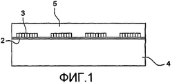
На фиг.1 показано устройство 1 неразрушающего контроля конструкции 4 в соответствии с настоящим изобретением, предназначенное для детектирования и измерения вибрационных волн, вызванных наличием дефекта в конструкции.Figure 1 shows the
Оно содержит гибкую подложку 2, в которую интегрированы средства 3 измерения вибрационных волн, излучаемых упомянутой конструкцией в различных точках поверхности конструкции. Гибкая подложка 2 выполнена, например, из пластического материала, позволяющего, таким образом, закрепить устройство на поверхности контролируемой конструкции, повторяя форму конструкции.It contains a
Гибкую подложку устройства 1 контроля неподвижно соединяют с поверхностью контролируемой конструкции 4 при помощи адгезивного материала.The flexible substrate of the
Предпочтительно это устройство закрепляют в критической зоне конструкции, где могут появиться трещины. На самолете устройство можно расположить в зонах, которые считаются критическими и находятся, например, на уровне зон подвески элеронов, на уровне зон соединения панелей, образующих фюзеляж, на уровне основных элементов крепления, например крепления двигателей.Preferably, this device is fixed in a critical area of the structure where cracks may appear. On an airplane, the device can be located in areas that are considered critical and are located, for example, at the level of the aileron suspension zones, at the level of the connection zones of the panels forming the fuselage, at the level of the main fastening elements, for example engine mounts.
Предпочтительно это устройство 1 контроля выполнено с возможностью нанесения на него слоя 5 покрытия, который может быть, например, слоем краски, которым покрывают устройство 1 контроля.Preferably, this
Средства измерения содержат решетку из пьезоэлектрических микродатчиков 3, предпочтительно сгруппированных в матрицу линий и столбцов. Каждый микродатчик выполнен с возможностью преобразования вибрационных волн, которые он принимает от конструкции, на которой он расположен, в электрические сигналы.The measuring means comprise a grid of
На фиг.2 схематично показан вид в разрезе одного из микродатчиков решетки. Он содержит набор пьезоэлектрических пластинок 6. Упомянутый набор пластинок расположен между двумя проводящими пластинами 8, 9.Figure 2 schematically shows a sectional view of one of the microsensors of the lattice. It contains a set of
Концы каждой пластинки неподвижно соединяют с двумя проводящими пластинами 8, 9 при помощи проводящего адгезивного материала 7, при этом одну из пластин неподвижно соединяют с гибкой подложкой 2, которая предназначена для покрытия поверхности контролируемой зоны конструкции.The ends of each plate are fixedly connected to two
Когда контролируемая конструкция вибрирует, пьезоэлектрические пластинки вибрируют на той же частоте, что и точка конструкции, где установлен микродатчик. Пластинки заряжаются электрически за счет пьезоэлектрического эффекта, деформируясь. Две проводящие пластины 8, 9, соединенные с концами пластинок, позволяют принимать электрические сигналы, генерируемые электрическими зарядами на пластинках.When the controlled structure vibrates, the piezoelectric plates vibrate at the same frequency as the point of the structure where the microsensor is mounted. The plates are charged electrically due to the piezoelectric effect, deforming. Two
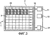
На фиг.3 схематично показан вид сверху устройства контроля согласно частному варианту выполнения изобретения, которое имеет по существу прямоугольную форму и содержит в данном случае, например, решетку из 56 пьезоэлектрических микродатчиков, сгруппированных в матрицу линий 3l и столбцов 3с. Кроме того, устройство предпочтительно содержит интерфейсную электронику 10, соединяющую решетку микродатчиков 3 с записывающим запоминающим устройством 11. Предпочтительно электроника 10 и запоминающее устройство 11 интегрированы в гибкую подложку 2 таким образом, чтобы при этом можно было получить монолитное устройство контроля.Figure 3 schematically shows a top view of a monitoring device according to a particular embodiment of the invention, which has a substantially rectangular shape and, in this case, contains, for example, a array of 56 piezoelectric microsensors grouped into an array of lines 3l and columns 3c. In addition, the device preferably comprises an
Электрические сигналы, принимаемые пластинами 8, 9 от каждого микродатчика, передаются на интерфейсную электронику 10, которая предпочтительно содержит средства усиления упомянутых электрических сигналов. После этого усиленные сигналы направляются в записывающее запоминающее устройство 11. Интерфейсная электроника 10 расположена на конце линий микродатчиков в варианте выполнения устройства, показанном на фиг.3. В другом варианте выполнения интерфейсная электроника может быть расположена на конце столбцов микродатчиков, однако в рамках настоящего изобретения возможны и другие относительные положения между микродатчиками и интерфейсной электроникой.The electrical signals received by the
Каждый микродатчик 3 выдает информацию о вибрациях конструкции в месте размещения микродатчика, и распределение микродатчиков позволяет получить картографию вибрационных волн на поверхности упомянутой конструкции таким образом, чтобы в зависимости от микродатчиков можно было локализовать дефект конструкции, вызывающий локальное изменение вибрационных волн.Each
Для точной локализации дефектов шаг между микродатчиками устанавливают в значении, меньшем минимальных размеров детектируемых дефектов, таким образом, чтобы можно было выделить положение дефектов, и чтобы в случае локального повреждения решетки из микродатчиков, микродатчики, находящиеся вокруг поврежденной зоны решетки могли позволять отслеживать зоны, достаточно близкие к возможному дефекту, чтобы дефект можно было действительно детектировать.For accurate localization of defects, the step between the microsensors is set to a value smaller than the minimum dimensions of the detected defects, so that the position of the defects can be distinguished, and so that in case of local damage to the grating from microsensors, the microsensors located around the damaged area of the grating can allow tracking zones that are sufficient close to a possible defect so that the defect can really be detected.
В частном варианте выполнения изобретения режим передачи электрических сигналов от микродатчиков 3 на интерфейсную электронику 10 является режимом межлинейной передачи. Над каждой линией микродатчиков расположена линия 23 накопления. Сигналы временно накапливаются в этой линии 23 накопления. Содержимое линий накопления передается затем на интерфейсную электронику 10 в параллельном режиме. Затем электрические сигналы последовательно направляются в записывающее запоминающее устройство 11.In a particular embodiment of the invention, the mode of transmission of electrical signals from
В варианте режима передачи электрических сигналов происходит обращение непосредственно к каждому микродатчику для передачи электрических сигналов непосредственно на интерфейсную электронику 10.In the embodiment of the mode of transmission of electrical signals, an appeal is made directly to each microsensor for transmitting electrical signals directly to the
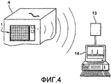
Для автоматической обработки электрических сигналов, измеренных микродатчиками 3, устройство контроля дополнительно содержит вычислительную систему 13, схематично показанную на фиг.4, для преобразования электрических сигналов, характерных для измеренных вибрационных волн, в цифровые значения и для определения вибрационных волн, вызванных наличием дефекта в конструкции, на основании вибрационных волн, измеренных микродатчиками. Вычислительная система является, например, системой с микропроцессором.For the automatic processing of electrical signals measured by
В предпочтительном варианте выполнения изобретения, показанном на фиг.4, вычислительная система не интегрирована в гибкую подложку 2, и устройство содержит средства передачи, показанные позицией 12 на фиг.3, для направления электрических сигналов, записанных в записывающем запоминающем устройстве 11, в вычислительную систему 13 с использованием беспроводной связи, радио или инфракрасной. Эти средства передачи содержат, например, приемоответчик, интегрированный в гибкую подложку, который предпочтительно работает на фиксированной частоте, при этом упомянутую частоту выбирают таким образом, чтобы передача электрических сигналов, характеризующих вибрации, не мешала передаче других данных другими устройствами, отличными от устройства контроля.In the preferred embodiment of FIG. 4, the computing system is not integrated into the
Предпочтительно вычислительная система содержит аналого-цифровой преобразователь для преобразования аналоговых электрических сигналов, поступающих из записывающего запоминающего устройства, в цифровые значения. Эти цифровые значения затем преобразуются в вибрационные волны благодаря средствам вычисления, в которые предпочтительно интегрируют теоретическую или экспериментальную модель, устанавливающую связь между детектированной вибрацией и генерируемым электрическим зарядом.Preferably, the computing system comprises an analog-to-digital converter for converting analog electrical signals from a recording memory to digital values. These digital values are then converted into vibrational waves by means of computation, which preferably integrates a theoretical or experimental model that establishes the relationship between the detected vibration and the generated electric charge.
Для определения изменений вибраций, вызванных наличием дефекта в конструкции, на основании вибрационных волн, измеренных микродатчиками, система содержит средства анализа для осуществления сравнительного исследования по амплитуде и по частоте между вибрационными волнами, измеренными микродатчиками, и контрольными вибрационными волнами. Для этого вычислительная система содержит запоминающее устройство, в котором хранится база картографических данных контрольных вибрационных волн конструкции. Контрольная картография представляет собой заранее определенную модель сравнения относительно поведения зоны, покрытой устройством контроля. Эта картография может быть определена заранее на контрольной конструкции. Под контрольной конструкцией следует понимать конструкцию, которая не содержит дефектов, например конструкцию на выходе производственной линии, прошедшую все этапы определения качества. Ее можно также заранее определить моделированием. Когда средства анализа осуществляют сравнение по амплитуде между контрольными вибрационными волнами и вибрационными волнами, измеренными микродатчиками, если определенное дифференциальное значение между контрольными вибрационными волнами и измеренными вибрационными волнами превышает пороговое значение, средства анализа генерируют сигнал состояния S.To determine changes in vibrations caused by the presence of a defect in the structure, based on vibration waves measured by microsensors, the system contains analysis tools for performing a comparative study in amplitude and frequency between vibration waves measured by microsensors and control vibration waves. For this, the computing system contains a storage device in which the base of cartographic data of the control vibrational waves of the structure is stored. Control cartography is a predefined comparison model regarding the behavior of the area covered by the control device. This mapping can be predefined on the control structure. A control structure should be understood as a structure that does not contain defects, for example, a structure at the output of a production line that has gone through all stages of quality determination. It can also be predefined by modeling. When the analysis tools perform an amplitude comparison between the control vibration waves and vibration waves measured by the microsensors, if the determined differential value between the control vibration waves and the measured vibration waves exceeds a threshold value, the analysis tools generate a state signal S.
Предпочтительно это сравнение по амплитуде дополняют спектральным анализом. Например, средства анализа прежде всего осуществляют Фурье-образ измеренных вибрационных волн для получения частотной характеристики вибрации, сравнивая частотную характеристику контрольных вибрационных волн и частотную характеристику измеренных вибрационных волн, при этом спектральные полосы, соответствующие вибрационным волнам, вызванным наличием дефекта в конструкции, выделяются средствами анализа, которые генерируют второй сигнал состояния S'.Preferably, this amplitude comparison is supplemented by spectral analysis. For example, the analysis tools first of all carry out the Fourier transform of the measured vibrational waves to obtain the frequency response of the vibration, comparing the frequency response of the control vibrational waves and the frequency response of the measured vibrational waves, while the spectral bands corresponding to the vibrational waves caused by the presence of a defect in the structure are distinguished by analysis means which generate a second state signal S '.
Предпочтительно спектральный анализ позволяет идентифицировать характер встречаемых дефектов. Как правило, вибрационный спектр содержит совокупность полос. Для облегчения идентификации полос, соответствующих дефектам, и их классификации по типу встречаемых дефектов предпочтительно в запоминающее устройство вычислительной системы записывают также библиотеку спектральных конфигураций.Preferably, spectral analysis allows the identification of the nature of the defects encountered. Typically, the vibrational spectrum contains a plurality of bands. To facilitate identification of the bands corresponding to defects and their classification by the type of defects encountered, a library of spectral configurations is also preferably recorded in the storage device of the computing system.
Сигналы состояния S и S', а также все данные, такие как характер дефектов, размер дефектов и место нахождения дефектов, передаются вычислительной системой на средства 14 тревожной сигнализации, которые содержат, например, экран отображения 22 для отображения данных и световые и/или звуковые индикаторы 20 для оповещения оператора, занимающегося обслуживанием.The state signals S and S ', as well as all data, such as the nature of the defects, the size of the defects and the location of the defects, are transmitted by the computer system to the alarm means 14, which comprise, for example, a
Передачу электрических сигналов, записанных в запоминающее устройство 11, в вычислительную систему можно запрограммировать таким образом, чтобы она производилась автоматически, например, в конце полета самолета. Эта передача может быть также активирована в ручном режиме оператором путем обращения к устройству контроля во время осмотра самолета.The transmission of electrical signals recorded in the
В другом варианте выполнения изобретения вычислительная система 13 интегрирована непосредственно в гибкую подложку 2 и соединена между интерфейсной электроникой 10 и записывающим запоминающим устройством 11. В этом варианте выполнения вычислительная система 13 напрямую принимает электрические сигналы от интерфейсной электроники 10 и направляет в записывающее запоминающее устройство 11 только сигналы состояния S и S' и данные о дефектах. Во время технического осмотра, обращаясь к устройству, оператор переправляет сигналы состояния и данные, записанные в запоминающем устройстве устройства контроля, в средства 14 тревожной сигнализации, используя беспроводную связь, радио или инфракрасную.In another embodiment, the
В рамках контроля конструкций в режиме реального времени устройство контроля можно, например, запрограммировать таким образом, чтобы активировать его, когда самолет уже не находится на земле, и оно после этого осуществляет измерения через равномерные промежутки времени, например через каждые 5 минут в течении определенного периода, чтобы создать картографию в зависимости от времени. Таким образом, устройство контроля позволяет получить картографию наблюдаемой зоны в зависимости от времени, чтобы установить изменение поля вибрационных волн, излучаемых деталью.As part of the real-time monitoring of structures, the monitoring device can, for example, be programmed in such a way as to activate it when the aircraft is no longer on the ground, and after that it takes measurements at regular intervals, for example, every 5 minutes for a certain period to create a mapping based on time. Thus, the control device allows you to get a cartography of the observed area depending on time to establish a change in the field of vibrational waves emitted by the part.
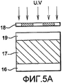
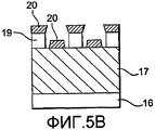
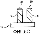
Решетку пластинок выполняют согласно технологиям, известным в области микроэлектроники. Решетку пластинок можно выполнить, например, при помощи УФ фотолитографии. На фиг.5А, 5В и 5С представлен пример выполнения пластинок по технологии фотолитографии. Пьезоэлектрическую пленку 17 наносят на твердую основу 16 типа кремния или стекла, при этом толщина пленки 17 может составлять от нескольких десятков нанометров до нескольких десятком микрон. На пьезоэлектрическую пленку наносят светочувствительную пленку, например смолу 19, и подвергают облучению УФ лучами через шаблон 18. На фиг.5В блок показан после погружения в ванну растворителя-проявителя и после процесса металлизации. Поверхность пьезоэлектрической пленки 17 содержит, таким образом, металлизированные зоны, нанесенные на поверхность пьезоэлектрической пленки, и зоны из смолы.The lattice of the plates is performed according to technologies known in the field of microelectronics. The lattice of the plates can be performed, for example, using UV photolithography. On figa, 5B and 5C presents an example of the implementation of the plates on the technology of photolithography. The
Исчезая в ванне растворителя зоны смолы, удаляют металл, который был нанесен на ее поверхность, оставляя на поверхности пьезоэлектрической пленки 17 требуемые металлические рисунки, которые образуют шаблон для этапа сухой гравировки. Нанесенный металл обладает намного более низкой способностью к гравировке, чем пьезоэлектрическая пленка 17, и, контролируя время гравировки и скорость гравировки, выполняют решетку пластинок с равномерными интервалами при помощи сухой гравировки через металлический шаблон. Ширина пластинок может составлять от нескольких десятков нанометров до нескольких микрометров, и шаг между пластинками может составлять от нескольких десятков нанометров до нескольких микрометров.When the resin zone disappears in the solvent bath, the metal that has been deposited on its surface is removed, leaving the required metal patterns on the surface of the
Для того чтобы расположить полученную таким образом решетку пластинок между двумя проводящими пластинами 8, 9, а затем интегрировать ее в гибкую подложку 8 для получения микродатчиков 3, сначала располагают первую проводящую пластину 8, которую крепят на решетке пластинок при помощи проводящего адгезивного материала 7. Затем твердую основу 16 можно снять путем лазерной абляции. После этого решетку пластинок крепят на второй пластине 9 при помощи проводящего адгезивного материала 7. На последнем этапе весь блок крепят на гибкой подложке 2 при помощи адгезива.In order to arrange the plate grid thus obtained between the two
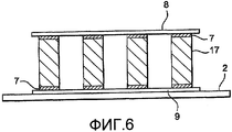
На фиг.6 показан вид сбоку в разрезе полученной таким образом решетки пьезоэлектрических пластинок 17, охваченных двумя проводящими пластинами 8, 9. Полученный микродатчик располагают через равномерные промежутки для реализации решетки из микродатчиков, например, показанной на фиг.3. В качестве материала для выполнения пьезоэлектрических пластинок используют, например, пленку из пьезоэлектрического материала 17 типа цирконата-титаната свинца (PZT). Предпочтительно пьезоэлектрические пластинки выполняют из материалов с повышенным пьезоэлектрическим коэффициентом и достаточно высокой температурой Кюри, которая является температурой, сверх которой материал теряет пьезоэлектричество, чтобы иметь возможность функционировать в области температур, с которыми сталкивается устройство во время своей работы.FIG. 6 shows a cross-sectional side view of the lattice of
Пьезоэлектрические пластинки предназначены для приема низкочастотных вибрационных волн, которые появляются при макроскопическом смещении конструкции вокруг неподвижного положения, а также высокочастотных волн, которые появляются при внутренних микроскопических смещениях материала.Piezoelectric plates are designed to receive low-frequency vibrational waves that appear during macroscopic displacement of the structure around a fixed position, as well as high-frequency waves that appear during internal microscopic displacements of the material.
Все другие электронные компоненты, интегрированные в гибкую подложку, выполнены по технологии микроскопического изготовления на твердой основе, такой как кремний или стекло, транспонированной в данном случае на пластическую основу. Температура, используемая во время процесса изготовления, может разрушить пластическую основу и поэтому не позволяет выполнять компоненты непосредственно на гибкой основе. Для решения этой технической проблемы, согласно одному из предлагаемых в настоящее время решений, сначала выполняют компоненты на твердой основе, нанесенной на стекло. Другой слой стекла, выполняющий функцию защиты, крепят на компонентах при помощи растворимого адгезива, после чего твердую основу извлекают из наслоения путем лазерной абляции. Затем компоненты накладывают на пластическую основу и крепят на ней при помощи постоянного адгезива, а защитное стекло удаляют.All other electronic components integrated into the flexible substrate are made using microscopic technology on a solid base, such as silicon or glass, transposed in this case to a plastic base. The temperature used during the manufacturing process can destroy the plastic base and therefore does not allow the components to be carried out directly on a flexible basis. To solve this technical problem, according to one of the currently proposed solutions, components are first made on a solid base applied to glass. Another layer of glass, which performs the function of protection, is attached to the components using a soluble adhesive, after which the solid base is removed from the lamination by laser ablation. Then the components are applied to the plastic base and fixed on it with a permanent adhesive, and the protective glass is removed.
Согласно частному варианту выполнения, устройство контроля имеет толщину, меньшую или равную 50 мкм, и поверхность со сторонами порядка 10 × 10 см. Размер каждого микродатчика составляет порядка сотни микрон, и интервал между двумя микродатчиками составляет порядка десятка микрон.According to a particular embodiment, the control device has a thickness less than or equal to 50 μm and a surface with sides of the order of 10 × 10 cm. The size of each microsensor is of the order of hundreds of microns, and the interval between two microsensors is of the order of ten microns.
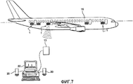
На фиг.7 схематично показана сеть из нескольких устройств контроля в соответствии с настоящим изобретением, расположенных на поверхностях конструкций самолета 15. Самолет находится на земле, и решетка устройств контроля находится в состоянии передачи сигналов, записанных во время полета или нескольких полетов самолета, в вычислительную систему 13, которая соединена со средствами тревожной сигнализации 14, которые в данном случае содержат, например, компьютер с экраном отображения и звуковые индикаторы 20.7 schematically shows a network of several monitoring devices in accordance with the present invention located on the surfaces of
Предпочтительно устройство содержит систему автопитания пьезоэлектрических микродатчиков, например, по меньшей мере, одна линия или один столбец микродатчиков устройства соединены с аккумулятором 21 электрической энергии, предназначенным для накапливания электрической энергии, генерируемой, по меньшей мере, одной линией или, по меньшей мере, одним столбцом микродатчиков под действием вибраций конструкции. Этот аккумулятор возвращает электрическую энергию в виде тока для питания устройства контроля.Preferably, the device comprises a piezoelectric microsensor self-feeding system, for example, at least one line or one column of microsensors of the device is connected to an
Изобретение представлено в рамках контроля конструкций летательных аппаратов, однако его можно применять для любой конструкции, на которую действуют источники возбуждения вибрации и которую необходимо контролировать для обнаружения наличия дефектов, например в других промышленных областях, таких как автомобильная промышленность, железнодорожный транспорт, судостроение или ядерная энергетика.The invention is presented in the framework of the control of aircraft structures, but it can be applied to any structure that is affected by vibration sources and which must be monitored to detect defects, for example, in other industrial fields, such as the automotive industry, railway transport, shipbuilding, or nuclear energy .
Claims (15)
Applications Claiming Priority (2)
| Application Number | Priority Date | Filing Date | Title |
|---|---|---|---|
| FR0651903 | 2006-05-24 | ||
| FR0651903A FR2901610B1 (en) | 2006-05-24 | 2006-05-24 | DEVICE FOR NON-DESTRUCTIVE CONTROL OF STRUTURE BY VIBRATION ANALYSIS |
Publications (2)
| Publication Number | Publication Date |
|---|---|
| RU2008151161A RU2008151161A (en) | 2010-06-27 |
| RU2435161C2 true RU2435161C2 (en) | 2011-11-27 |
Family
ID=37622215
Family Applications (1)
| Application Number | Title | Priority Date | Filing Date |
|---|---|---|---|
| RU2008151161/28A RU2435161C2 (en) | 2006-05-24 | 2007-05-16 | Device for non-destructive check of structure by means of vibration analysis |
Country Status (9)
| Country | Link |
|---|---|
| US (1) | US8151643B2 (en) |
| EP (1) | EP2027461A1 (en) |
| JP (1) | JP5450058B2 (en) |
| CN (1) | CN101449157B (en) |
| BR (1) | BRPI0712212A2 (en) |
| CA (1) | CA2650832A1 (en) |
| FR (1) | FR2901610B1 (en) |
| RU (1) | RU2435161C2 (en) |
| WO (1) | WO2007135057A1 (en) |
Cited By (4)
| Publication number | Priority date | Publication date | Assignee | Title |
|---|---|---|---|---|
| RU2566418C1 (en) * | 2014-07-22 | 2015-10-27 | Федеральное государственное бюджетное образовательное учреждение высшего профессионального образования "Московский государственный университет приборостроения и информатики" | Magnetic flaw detection method |
| WO2017180007A1 (en) * | 2016-04-14 | 2017-10-19 | Виталий Иванович СУРИН | Method for local detection of flaws and device for realizing such a method (variants) |
| RU2643941C1 (en) * | 2016-10-19 | 2018-02-06 | Федеральное государственное бюджетное образовательное учреждение высшего образования "Морской государственный университет имени адмирала Г.И. Невельского" | Piezo electric element for installation on flexible base structure |
| RU2654949C1 (en) * | 2014-07-11 | 2018-05-23 | Микротек Медикал Текнолоджиз Лтд. | Multi-element transducer |
Families Citing this family (26)
| Publication number | Priority date | Publication date | Assignee | Title |
|---|---|---|---|---|
| DE102008003498B4 (en) | 2008-01-08 | 2022-09-01 | Airbus Defence and Space GmbH | Impact detection element for an aircraft, impact detection device constructed therewith, and method for monitoring impact processes on an aircraft |
| WO2009101978A1 (en) * | 2008-02-13 | 2009-08-20 | National University Corporation Kyoto Institute Of Technology | Method and device of diagnosing damage of structural object |
| US8181524B2 (en) * | 2008-12-26 | 2012-05-22 | Panasonic Corporation | Ultrasonic stress measurement method and device |
| US8408065B2 (en) * | 2009-03-18 | 2013-04-02 | Bp Corporation North America Inc. | Dry-coupled permanently installed ultrasonic sensor linear array |
| GB201018259D0 (en) * | 2010-10-29 | 2010-12-15 | Airbus Operations Ltd | Ultrasonic inspection tool |
| CN103221148B (en) * | 2010-11-18 | 2016-04-13 | 皇家飞利浦电子股份有限公司 | There are the Medical Devices of the ultrasonic transducer be embedded in flexible paillon foil |
| FR2974900B1 (en) * | 2011-05-02 | 2013-05-17 | Aircelle Sa | MONITORING ASSEMBLY AND METHOD FOR DETECTING STRUCTURAL DEFECTS MAY APPEAR IN AN AIRCRAFT NACELLE |
| CN102393445A (en) * | 2011-10-24 | 2012-03-28 | 沈阳建筑大学 | Pipeline structure damage monitoring method based on piezoelectric ceramic sensor and guide wave analysis |
| US20130132035A1 (en) * | 2011-11-23 | 2013-05-23 | Ge Aviation Systems Llc | Method for diagnosing a health of an apparatus |
| US20130132033A1 (en) * | 2011-11-23 | 2013-05-23 | Ge Aviation Systems Llc | System and apparatus for radiation diagnosis |
| FR2987443B1 (en) * | 2012-02-24 | 2014-03-07 | Snecma | DEVICE FOR DETECTING ANOMALIES BY ACOUSTIC ANALYSIS OF AN AIRCRAFT TURBOMACHINE |
| US9511393B2 (en) * | 2012-08-17 | 2016-12-06 | The Boeing Company | Flexible ultrasound inspection system |
| CN104931510A (en) * | 2015-06-30 | 2015-09-23 | 山东大学 | Aluminum alloy structure micro-damage detection system and method |
| US10460536B2 (en) | 2015-08-04 | 2019-10-29 | Sikorsky Aircraft Corporation | Rotorcraft structural fault-detection and isolation using virtual monitoring of loads |
| JP6078860B1 (en) * | 2016-04-15 | 2017-02-15 | 学校法人神奈川大学 | Vibration detection apparatus, vibration characteristic measurement system, and vibration characteristic measurement method |
| EP3258258A1 (en) * | 2016-06-13 | 2017-12-20 | Airbus Defence and Space GmbH | Sensor skin |
| US9965939B2 (en) * | 2016-09-01 | 2018-05-08 | Locus Solutions, Llc | Systems and methods for monitoring vibrations during transportation of goods |
| FR3065526B1 (en) * | 2017-04-24 | 2019-07-19 | Flight Level & Orbital Deployment | SYSTEM FOR DETECTING A STATE OR DYSFUNCTION BY VIBRATION ANALYSIS |
| CN107804455A (en) * | 2017-10-23 | 2018-03-16 | 南京航空航天大学 | Piezoelectric intelligent composite material rotor |
| CN108169037B (en) * | 2017-12-15 | 2019-03-29 | 南京航空航天大学 | Continuous heterogeneous large area Impact monitoring network and shock zone localization method |
| CN108303278B (en) * | 2018-02-05 | 2020-05-05 | 青岛云世纪信息科技有限公司 | Method and device for detecting takeoff state of paddle type aircraft |
| DE102018210500A1 (en) * | 2018-06-27 | 2020-01-02 | MTU Aero Engines AG | Method and device for non-destructive acoustic examination of at least a region of a component of a turbomachine |
| KR102482508B1 (en) * | 2018-11-06 | 2022-12-28 | 제이에프이 스틸 가부시키가이샤 | Method for determining elastic matrix of laminated iron core and method for analyzing vibration |
| EP3748327A1 (en) | 2019-06-07 | 2020-12-09 | Ostbayerische Technische Hochschule Regensburg | Method and system for evaluating a structural integrity of an aerial vehicle |
| CN110502972A (en) * | 2019-07-05 | 2019-11-26 | 广东工业大学 | A kind of pavement crack segmentation and recognition methods based on deep learning |
| CN113205036A (en) * | 2021-04-28 | 2021-08-03 | 同济大学 | Sensing and positioning method for external invasion vibration source of infrastructure |
Family Cites Families (46)
| Publication number | Priority date | Publication date | Assignee | Title |
|---|---|---|---|---|
| FR1403635A (en) | 1963-08-14 | 1965-06-25 | Massiot Philips Sa | Device for the visual reproduction of images by television |
| JPS4413461B1 (en) * | 1966-05-18 | 1969-06-17 | ||
| US3511086A (en) | 1966-11-23 | 1970-05-12 | Boeing Co | Nondestructive testing with liquid crystals |
| US3970074A (en) | 1974-08-22 | 1976-07-20 | Spitalul Clinic Filantropia Bucuresti | Method of and apparatus for making medical thermographs |
| US4433637A (en) | 1979-06-04 | 1984-02-28 | Vectra International Corporation | Microencapsulated cholesteric liquid crystal temperature measuring device for determining the temperature of non-planar or planar surfaces |
| US4295111A (en) * | 1979-11-29 | 1981-10-13 | Nasa | Low temperature latching solenoid |
| FR2598250B1 (en) | 1986-04-30 | 1988-07-08 | Thomson Csf | RADIOLOGICAL PICTURE PANEL, AND MANUFACTURING METHOD |
| JPH0225717A (en) * | 1988-07-15 | 1990-01-29 | Hitachi Ltd | Oscillation sensor |
| GB8819487D0 (en) * | 1988-08-16 | 1988-09-21 | Pennwalt Piezo Film Ltd | Sensing breakage of glass |
| JP2707127B2 (en) * | 1988-12-28 | 1998-01-28 | 株式会社いすゞセラミックス研究所 | Electromagnetic valve drive |
| US5166573A (en) * | 1989-09-26 | 1992-11-24 | Atochem North America, Inc. | Ultrasonic contact transducer and array |
| US5034714A (en) * | 1989-11-03 | 1991-07-23 | Westinghouse Electric Corp. | Universal relay |
| US5047719A (en) | 1990-05-25 | 1991-09-10 | The Failure Group, Inc. | Flexible coil assembly for reflectance-mode nondestructive eddy-current examination |
| US5293555A (en) * | 1991-05-24 | 1994-03-08 | Hughes Aircraft Company | System and method for locating material fatigue using multiple sensors |
| US5184516A (en) * | 1991-07-31 | 1993-02-09 | Hughes Aircraft Company | Conformal circuit for structural health monitoring and assessment |
| US5315234A (en) | 1992-04-03 | 1994-05-24 | General Electric Company | Eddy current device for inspecting a component having a flexible support with a plural sensor array |
| DE4220544B4 (en) | 1992-06-24 | 2005-10-20 | Woelfel Horst | Method for measuring mechanical stress components on the surface of dynamically loaded DUTs |
| JPH06113387A (en) * | 1992-09-25 | 1994-04-22 | Railway Technical Res Inst | Sound image visualizing device for sound source observation |
| JP3288815B2 (en) * | 1993-06-30 | 2002-06-04 | 株式会社東芝 | 2D array ultrasonic probe |
| IT1273248B (en) | 1994-03-15 | 1997-07-07 | Europiana S R L | APPARATUS FOR MEASURING THE TEMPERATURE OF THE SKIN |
| US5659248A (en) | 1994-10-17 | 1997-08-19 | General Electric Company | Multilayer eddy current probe array for complete coverage of an inspection surface without mechanical scanning |
| US5793206A (en) | 1995-08-25 | 1998-08-11 | Jentek Sensors, Inc. | Meandering winding test circuit |
| US5911158A (en) * | 1996-02-29 | 1999-06-08 | The United States Of America As Represented By The Secretary Of The Air Force | Piezoelectric strain sensor array |
| JP3194078B2 (en) * | 1996-03-29 | 2001-07-30 | 日本鋼管株式会社 | Vibration detector with spontaneous power supply |
| JP3673035B2 (en) * | 1996-10-25 | 2005-07-20 | 株式会社東芝 | Ultrasonic transducer |
| JPH10281859A (en) * | 1997-04-07 | 1998-10-23 | Mitsui Eng & Shipbuild Co Ltd | Abnormality diagnostic method and device |
| US5915277A (en) * | 1997-06-23 | 1999-06-22 | General Electric Co. | Probe and method for inspecting an object |
| JPH1164089A (en) * | 1997-08-18 | 1999-03-05 | Toshiba Corp | Wave motion diagnostic equipment |
| GB9808668D0 (en) * | 1998-04-24 | 1998-06-24 | Smiths Industries Plc | Monitoring |
| US6077228A (en) | 1998-11-04 | 2000-06-20 | Schonberger; Milton | Breast temperature scanner |
| US6370964B1 (en) * | 1998-11-23 | 2002-04-16 | The Board Of Trustees Of The Leland Stanford Junior University | Diagnostic layer and methods for detecting structural integrity of composite and metallic materials |
| US6399939B1 (en) * | 2000-06-13 | 2002-06-04 | North Carolina A&T State University | Sensor array system |
| JP2002027594A (en) * | 2000-07-11 | 2002-01-25 | Hitachi Ltd | Ultrasonic probe and method for manufacturing the same |
| US6564640B1 (en) * | 2000-11-28 | 2003-05-20 | Quality Research, Development & Consulting, Inc. | Smart skin structures |
| DE10136756C2 (en) | 2001-07-27 | 2003-07-31 | Siemens Ag | X-ray diagnostic device with a flexible solid-state X-ray detector |
| JP2003130853A (en) * | 2001-10-24 | 2003-05-08 | National Institute Of Advanced Industrial & Technology | Damage sensing sheet |
| FR2836994B1 (en) | 2002-03-05 | 2004-12-17 | Airbus France | METHOD AND DEVICE FOR CHECKING PARTS BY X-RAY |
| US6739195B2 (en) * | 2002-04-09 | 2004-05-25 | The United States Of America As Represented By The Secretary Of The Army | System and method for determining the status of an object by insonification |
| JP2004088056A (en) * | 2002-07-02 | 2004-03-18 | Sumitomo Electric Ind Ltd | Piezoelectric vibrator, mounting method for it, mounting device, ultrasonic probe using it, and three-dimensional ultrasonic diagnostic device using it |
| JP4102710B2 (en) * | 2003-06-04 | 2008-06-18 | 富士重工業株式会社 | Structure diagnosis method and apparatus for hollow structure |
| JP3812559B2 (en) | 2003-09-18 | 2006-08-23 | Tdk株式会社 | Eddy current probe |
| US7285897B2 (en) * | 2003-12-31 | 2007-10-23 | General Electric Company | Curved micromachined ultrasonic transducer arrays and related methods of manufacture |
| JP4443247B2 (en) * | 2004-01-28 | 2010-03-31 | 株式会社日立製作所 | Status monitoring system and status monitoring method |
| FR2874430B1 (en) * | 2004-08-23 | 2007-03-30 | Eads Ccr Groupement D Interet | INTEGRATED PIEZOELECTRIC FILM ASSEMBLY FOR NON-DESTRUCTIVE CONTROL OF THIS ASSEMBLY |
| US7430911B2 (en) * | 2004-08-26 | 2008-10-07 | Acellent Technologies, Inc. | Method of detecting and analyzing changes in the external loading conditions of a structure |
| US7719394B2 (en) * | 2004-10-06 | 2010-05-18 | Victor Nelson | Latching linear solenoid |
-
2006
- 2006-05-24 FR FR0651903A patent/FR2901610B1/en not_active Expired - Fee Related
-
2007
- 2007-05-16 CN CN2007800186687A patent/CN101449157B/en not_active Expired - Fee Related
- 2007-05-16 RU RU2008151161/28A patent/RU2435161C2/en not_active IP Right Cessation
- 2007-05-16 WO PCT/EP2007/054759 patent/WO2007135057A1/en active Application Filing
- 2007-05-16 JP JP2009511473A patent/JP5450058B2/en not_active Expired - Fee Related
- 2007-05-16 CA CA002650832A patent/CA2650832A1/en not_active Abandoned
- 2007-05-16 BR BRPI0712212-8A patent/BRPI0712212A2/en not_active IP Right Cessation
- 2007-05-16 EP EP07729207A patent/EP2027461A1/en not_active Withdrawn
- 2007-05-16 US US12/301,702 patent/US8151643B2/en not_active Expired - Fee Related
Cited By (6)
| Publication number | Priority date | Publication date | Assignee | Title |
|---|---|---|---|---|
| RU2654949C1 (en) * | 2014-07-11 | 2018-05-23 | Микротек Медикал Текнолоджиз Лтд. | Multi-element transducer |
| US10847708B2 (en) | 2014-07-11 | 2020-11-24 | Microtech Medical Technologies Ltd. | Multi-cell transducer |
| US11800806B2 (en) | 2014-07-11 | 2023-10-24 | Microtech Medical Technologies Ltd. | Method for manufacturing a multi-cell transducer |
| RU2566418C1 (en) * | 2014-07-22 | 2015-10-27 | Федеральное государственное бюджетное образовательное учреждение высшего профессионального образования "Московский государственный университет приборостроения и информатики" | Magnetic flaw detection method |
| WO2017180007A1 (en) * | 2016-04-14 | 2017-10-19 | Виталий Иванович СУРИН | Method for local detection of flaws and device for realizing such a method (variants) |
| RU2643941C1 (en) * | 2016-10-19 | 2018-02-06 | Федеральное государственное бюджетное образовательное учреждение высшего образования "Морской государственный университет имени адмирала Г.И. Невельского" | Piezo electric element for installation on flexible base structure |
Also Published As
| Publication number | Publication date |
|---|---|
| CN101449157A (en) | 2009-06-03 |
| FR2901610B1 (en) | 2009-01-16 |
| RU2008151161A (en) | 2010-06-27 |
| EP2027461A1 (en) | 2009-02-25 |
| CN101449157B (en) | 2013-07-10 |
| JP5450058B2 (en) | 2014-03-26 |
| BRPI0712212A2 (en) | 2012-03-13 |
| US20090301197A1 (en) | 2009-12-10 |
| WO2007135057A1 (en) | 2007-11-29 |
| CA2650832A1 (en) | 2007-11-29 |
| JP2009537835A (en) | 2009-10-29 |
| FR2901610A1 (en) | 2007-11-30 |
| US8151643B2 (en) | 2012-04-10 |
Similar Documents
| Publication | Publication Date | Title |
|---|---|---|
| RU2435161C2 (en) | Device for non-destructive check of structure by means of vibration analysis | |
| US7434480B2 (en) | Methods and systems for using active surface coverings for structural assessment and monitoring | |
| US7725269B2 (en) | Sensor infrastructure | |
| Lin et al. | Smart layer and smart suitcase for structural health monitoring applications | |
| US8447530B2 (en) | High density structural health monitoring system and method | |
| US7925455B2 (en) | Method and system for the determination of damage location | |
| RU2439549C2 (en) | Non-destructive test device of part by analysis of magnetic leakage field | |
| Misra et al. | An IoT based building health monitoring system supported by cloud | |
| US10793294B2 (en) | Nano-energetic applications for aircraft | |
| Kessler et al. | Design of a piezoelectric-based structural health monitoring system for damage detection in composite materials | |
| RU2439545C2 (en) | Non-destructive test device by means of radiation dispersion analysis | |
| Kessler et al. | Structural health monitoring of composite materials using piezoelectric sensors | |
| Kessler et al. | In-situ sensor-based damage detection of composite materials for structural health monitoring | |
| Mueller et al. | Effects of debonding of PWAS on the wave propagation and the electro-mechanical impedance spectrum | |
| Lin et al. | Built-in structural diagnostic with the SMART LayerTM and SMART SuitcaseTM | |
| Marantidis et al. | Sensors and sensing technologies for structural health monitoring of aircraft | |
| Kurnyta et al. | Assessment of sensor technologies for aircraft SHM systems | |
| Kessler et al. | Kessler | |
| Ursu et al. | Qualification of PWAS-Based SHM technology for space applications | |
| Weihnacht et al. | Smart monitoring and SHM | |
| Viscardi et al. | Numerical Simulation For ANN Training and validation For Impact Detection | |
| Pinsonnault | Condition-Based Maintenance | |
| Masson et al. | Signal processing strategies using micro-systems for in situ health monitoring of aircraft | |
| Spearing | IN-SITU SENSOR-BASED DAMAGE DETECTION OF COMPOSITE MATERIALS FOR STRUCTURAL HEALTH MONITORING | |
| Boller | Smart Systems for Enhanced Integrity of Existing and Future Structures |
Legal Events
| Date | Code | Title | Description |
|---|---|---|---|
| MM4A | The patent is invalid due to non-payment of fees |
Effective date: 20170517 |