KR930000966B1 - Non-linear resonant switch and converter - Google Patents
Non-linear resonant switch and converter Download PDFInfo
- Publication number
- KR930000966B1 KR930000966B1 KR1019890012641A KR890012641A KR930000966B1 KR 930000966 B1 KR930000966 B1 KR 930000966B1 KR 1019890012641 A KR1019890012641 A KR 1019890012641A KR 890012641 A KR890012641 A KR 890012641A KR 930000966 B1 KR930000966 B1 KR 930000966B1
- Authority
- KR
- South Korea
- Prior art keywords
- current
- switch
- resonant
- nonlinear
- primary
- Prior art date
Links
Images


Classifications
-
- H—ELECTRICITY
- H03—ELECTRONIC CIRCUITRY
- H03K—PULSE TECHNIQUE
- H03K17/00—Electronic switching or gating, i.e. not by contact-making and –breaking
-
- H—ELECTRICITY
- H02—GENERATION; CONVERSION OR DISTRIBUTION OF ELECTRIC POWER
- H02M—APPARATUS FOR CONVERSION BETWEEN AC AND AC, BETWEEN AC AND DC, OR BETWEEN DC AND DC, AND FOR USE WITH MAINS OR SIMILAR POWER SUPPLY SYSTEMS; CONVERSION OF DC OR AC INPUT POWER INTO SURGE OUTPUT POWER; CONTROL OR REGULATION THEREOF
- H02M3/00—Conversion of dc power input into dc power output
- H02M3/02—Conversion of dc power input into dc power output without intermediate conversion into ac
- H02M3/04—Conversion of dc power input into dc power output without intermediate conversion into ac by static converters
- H02M3/10—Conversion of dc power input into dc power output without intermediate conversion into ac by static converters using discharge tubes with control electrode or semiconductor devices with control electrode
- H02M3/145—Conversion of dc power input into dc power output without intermediate conversion into ac by static converters using discharge tubes with control electrode or semiconductor devices with control electrode using devices of a triode or transistor type requiring continuous application of a control signal
- H02M3/155—Conversion of dc power input into dc power output without intermediate conversion into ac by static converters using discharge tubes with control electrode or semiconductor devices with control electrode using devices of a triode or transistor type requiring continuous application of a control signal using semiconductor devices only
Landscapes
- Engineering & Computer Science (AREA)
- Power Engineering (AREA)
- Dc-Dc Converters (AREA)
Abstract
내용 없음.No content.
Description
제1도는 본 발명에 따른 콘버터의 일반화된 비선형공진스위치의 개략회로도.1 is a schematic circuit diagram of a generalized nonlinear resonant switch of a converter according to the present invention.
제2도는 제1도의 회로에 사용된 리액터에서의 코어자속대전류의 설명도.2 is an explanatory diagram of a core magnetic flux large current in a reactor used in the circuit of FIG.
제3도는 제1도 회로의 이상적인 경우에 대한 회로인덕턴스대 스위치전류의 설명도.3 is an explanatory diagram of circuit inductance vs. switch current for the ideal case of FIG.
제4도는 제1도 회로에 대한 피이드백 스위치제어기의 개략도.4 is a schematic diagram of a feedback switch controller for the FIG. 1 circuit.
제5도는 본 발명에 따른 반파 벅(Buck) 타입 비선형공진스위치 콘버터의 개략회로도.5 is a schematic circuit diagram of a half-wave Buck type nonlinear resonant switch converter according to the present invention.
제6도는 본 발명에 따른 전파 벅타입 비선형공진스위치 콘버터의 개략회로도.6 is a schematic circuit diagram of a full-wave buck type nonlinear resonant switch converter according to the present invention.
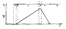
제7a도 및 7b도는 각각 시간대 스위치 전류와 커패시터 전압도.7A and 7B are time zone switch current and capacitor voltage diagrams, respectively.
제8도는 본 발명에 따른 전파 벅부우스트(Buck-Boost) 비선형공진스위치 콘버터의 개략회로도.8 is a schematic circuit diagram of a radio wave Buck-Boost nonlinear resonant switch converter according to the present invention.
제9도는 본 발명에 따른 전파부우스트 타입 비선형공진스위치 콘버터의 개략회로도.9 is a schematic circuit diagram of a radio wave boost type nonlinear resonant switch converter according to the present invention.
* 도면의 주요부분에 대한 부호의 설명* Explanation of symbols for main parts of the drawings
10 : 공진비선형스위치 12 : 입력단자(1차단자)10: Resonant nonlinear switch 12: Input terminal (primary terminal)
14 : 전압공급기 16 : 출력단자(2차단자)14: Voltage supply 16: Output terminal (secondary terminal)
18,24 : 인덕터 19,26 : 커패시터18,24:
20 : 부하 22 : 반도체스위치소자(반도체스위치수단)20 load 22 semiconductor switch element (semiconductor switch means)
28 : 1차권선 32 : 2차권선28: primary winding 32: secondary winding
30 : 자기코어 34 : 보조권선30: magnetic core 34: auxiliary winding
35,56 : 다이오드 38 : 코어바이어스회로(포화수단)35,56: diode 38: core bias circuit (saturation means)
40 : 퍼이드백스위치제어기(타이밍수단)40: feedback switch controller (timing means)
42 : VCO 50 :영교차검파기42: VCO 50: English cross detector
54 : FET54: FET
본 발명은 공진스위치에 관한 것으로 특히 파워변환장치에 유용한 비선형공진스위치 및 그러한 스위치를 사용하는 콘버터에 관한 것이다.The present invention relates to resonant switches, and more particularly to nonlinear resonant switches useful in power converters and converters using such switches.
파워변환기술분야에서, 콘버터사이즈, 무게 및 단가를 줄이기위한 목적으로 콘버터의 동작주파수를 증가시키는 추세에 있다.In the field of power conversion technology, there is a trend to increase the operating frequency of the converter for the purpose of reducing the converter size, weight and cost.
스위칭주파수의 증가는 콘버터의 트랜스와 수동필터구성소자의 사이즈의 현저한 감소를 가져온다. 종래의 펄스폭변조론버터는 각 퍽스의 끝에서 전류흐름을 종료하기위한 트런지스터스위칭을 사용한다. 스위칭주파수에 선형적으로 증가하는 트랜지스터스위칭 손실은 스위칭주파수의 증가에 주장애가 된다.Increasing the switching frequency results in a significant reduction in the size of the converter's transformer and passive filter components. Conventional pulse width modulation converters use transistor switching to terminate the current flow at the end of each pux. Transistor switching losses that increase linearly with the switching frequency present a major obstacle to the increase in the switching frequency.
누설인덕턴스와 권선용량같은 트랜스의 비이상적성질은 또한 고주파수에서 매우 중대한 문제가 되며, 콘버터효율을 저하시킬 수도 있다. 최근, 공진스위치 콘버터에서의 파워손실의 일부 또는 모든 원인을 제거하려는 연구가 시도되었으며, 그에 따라 높은 동작주파수에서 양호한 효율을 얻게되었다.The non-ideal nature of the transformer, such as leakage inductance and winding capacitance, is also a very significant problem at high frequencies and can reduce converter efficiency. Recently, a study has been attempted to eliminate some or all causes of power loss in a resonant switch converter, thereby obtaining good efficiency at a high operating frequency.
이 부류는 콘버터가 트랜지스터 파워스위치에 연합하여 동작되는 선형공진탱크소자로 이루어져, 영전압 또는 영전류에서 트랜지스터가 온/오프스위치하게 되며, 그러므로서 스위칭손실이 크게 줄어드는 것으로 나타난다. 공진탱크소자 또한 비 이상적성질의 트랜스에 빈번히 직렬 또는 병렬로 되므로 트랜시의 누설인덕턴스 및/또는 권선용량은 콘버터의 동작을 저하시키지 않는다.This class consists of a linear resonant tank element in which a converter is operated in conjunction with a transistor power switch, which causes the transistor to switch on / off at zero voltage or zero current, thus reducing switching losses significantly. The resonant tank element is also frequently in series or in parallel with non-ideal transformers so that the leakage inductance and / or winding capacitance of the transceiver does not degrade the operation of the converter.
콘버터동작주파수는 상기 기술을 사용하여 1 또는 2승 증가시킬 수 있게된다. 미국특허 제4,415,959호는 에너지원에 직렬로 연결된 스위칭장치와 스위치를 통한 전류펄스를 실행하기위한 LC회로를 가지는 DC-DC콘버터를 개시하고 있다.The converter operating frequency can be increased by one or two powers using the above technique. U.S. Patent No. 4,415,959 discloses a DC-DC converter having a switching device connected in series to an energy source and an LC circuit for executing a current pulse through the switch.
제어회로는 전튜가 영일때 스위치를 온/오프하여 스위칭손실을 제거한다. 1985년판 IEEE파워 일렉트로닉스 스페샬리스트콘퍼런스(Power Electronics Specialists Conference)의 페이지 106-116의 류와리(Liu and Lee)에 의한 보고서 ″공진스위치-형상 및 특성(Resonant Switches-Topologies and Characteris-tics)″에는 반파 및 전파공진스위치의 구성과 벅, 부우스트 및 벅/부우스트공진스위치 콘버터를 포함하는 여러종류의 콘버터회로에 대한 공진스위치의 응용을 논하고 있다.The control circuit eliminates switching losses by turning the switch on and off when the switch is zero. Half-wave for report ″ Resonant Switches-Topologies and Characteris-tics ″ by Liu and Lee, pages 106-116 of the 1985 edition of the IEEE Power Electronics Specialists Conference. And the application of resonant switches to various types of converter circuits including buck, boost and buck / boost resonant switch converters.
1987년판 IEEE 일렉트로닉스스페샬리스트 콘퍼런스의 페이지 395-403의 노(Ngo)에 의한 보고서 ″공진스위치 및 준공진 DC-DC 콘버터의 일반화(Generaliz ation of Resonant Switches and Qusai-Resonant DC-CD Converters)″에는 콘버터에 응용되는 공진스위치를 더 논의 및 분석하고 있다.A report by Ngo on pages 395-403 of the IEEE Electronics Specialist Conference, 1987, published in the Generalization of Resonant Switches and Qusai-Resonant DC-CD Converters. The resonant switch applied to this is further discussed and analyzed.
여러종류의 PWM(Pulse Width Modulated) 콘버터는 영전류 스위칭을 달성하 한 공진스위치동작에 적합하게 될 수 있으므로 일반적으로 무스위칭손실을 실현할 수 있는 것으로 알려져 있다.It is known that various kinds of PWM (Pulse Width Modulated) converters can be adapted to the resonant switch operation to achieve zero current switching.
한편, 앞에서 제안된 공진스위치 콘버터는, 출력전류와 파워가 같은 경우, 공진준 정현파형이 종래의 PWM콘버터의 구형파 피이크값보다 더 높은 값으로 나타나는 불이익이 있다. 따라서, 공진스위치 콘버터는 트랜지스터에서 높은 도통손실이 나타나고, 이러한 증가된 도통손실은, 스위칭손실을 제거하는 것으로 만들어지는 이득을 부분적 또는 전체적으로 무효하게 할 수 있다. 비록 파워 FET가 파워변환장치에서의 스위칭을 위한 소정의 특성을 가진다해도, FET는 큰 저항을 가진다. 따라서, 손실을 최소화하기위해 피이크전류를 최소화로하는 것이 중요하다.On the other hand, the resonant switch converter proposed above has a disadvantage in that when the output current and the power are the same, the resonant quasi-sinusoidal waveform has a higher value than the square wave peak value of the conventional PWM converter. Thus, the resonant switch converter exhibits high conduction loss in the transistor, and this increased conduction loss can partially or totally invalidate the gain made by eliminating the switching loss. Although the power FET has certain characteristics for switching in the power converter, the FET has a large resistance. Therefore, it is important to minimize the peak current to minimize losses.
본 발명의 목적은 종재의 PWM장치의 낮은 피이크전류를 유지하는 동안 스위칭손실을 제거하는 파워변환에 유용한 스위치와 그러한 스위치를 사용하는 콘버터를 제공하는 데 있다.It is an object of the present invention to provide a switch useful for power conversion that eliminates switching losses while maintaining a low peak current of the final PWM device and a converter using such a switch.
본 발명에 따른 비선형공진스위치 및 비선형공진스위치 콘버터는 각기 특허청구범위 제1항과 제7항으로 특징지워진다.The nonlinear resonant switch and the nonlinear resonant switch converter according to the present invention are characterized by
본 발명은 자기코어상에 1차권선과 2차권선이 형성된 자기코어를 포함하는 비선형리액터 ; 낮은 1차권선 전류에서 자기코어를 포화시키고 높은 1차권선전류에서 불포화시키는 포화수단과 ; 상기 1차권선과 커패시터를 포함하는 공진탱크회로와 상기 공진탱크회로에 직렬로 연결되는 반도체스위치수단을 포함하여, 피이크 탱크회로전류를 불포화상태에 있는 비선형리액터의 인덕턴스로 감쇄시키는 1차회로 ; 탱크공진에 관련된 반도체스위칭수단의 스위칭이 반도체스위칭수단을 통하는 전류가 영일때 이루어지도록 타이밍하여 스위칭효율을 적정화하기 위한 타이밍수단 ; 커패시터에 병렬로 연결된 다이오드 ; 및 2차권선과 직렬인 다이오드와 커패시터조합을 포함하는 2차회로 ; 를 포함하는 비선형공진스위치로서 성취된다.The present invention provides a nonlinear reactor including a magnetic core having a primary winding and a secondary winding formed on a magnetic core; Saturating means for saturating the magnetic core at low primary winding currents and unsaturated at high primary winding currents; A primary circuit for reducing the peak tank circuit current to an inductance of a nonlinear reactor in an unsaturated state, including a resonant tank circuit including the primary winding and a capacitor and a semiconductor switch means connected in series with the resonant tank circuit; Timing means for optimizing switching efficiency by timing the switching of the semiconductor switching means associated with the tank resonance to occur when the current through the semiconductor switching means is zero; Diodes connected in parallel to a capacitor; And a secondary circuit comprising a diode and capacitor combination in series with the secondary winding; It is achieved as a non-linear resonant switch comprising a.
본 발명은 본 발명에 따른 비선형공진스위치를 실용화하는 콘버터에 의해 더 성처된다.The present invention is further achieved by a converter for practical use of the nonlinear resonant switch according to the present invention.
이하 본 발명의 일실시예를 설명한다.Hereinafter, an embodiment of the present invention will be described.
여기에 기술된 비선형공진스위치는 이전의 공진스위치구조의 영전류스위칭과 종래의 PWM 큰버터의 낮은 피이크전류를 결합시킨 것이다. 비선형탱크회로는 링깅전류를 왜곡시켜 피이크값이 줄어들도록 고안되었다.The nonlinear resonant switch described here combines the zero current switching of the previous resonant switch structure with the low peak current of a conventional PWM large butter. Nonlinear tank circuit is designed to reduce peak value by distorting ringing current.
트랜지스터스위칭은 영전류에서 일어나지만 피이크전류는 종래의 PWM 콘버터의 피이크전류보다 단지 10-20% 더 크게 되어야 한다. 조절된 포화인덕터의 사용으로 상기의 파형을 얻을 수 있다. 조절된 포화인 덕터의 사용으로 상기의 파형을 얻을 수 있다.Transistor switching occurs at zero current but the peak current should be only 10-20% greater than the peak current of a conventional PWM converter. The waveform can be obtained by using a controlled saturation inductor. The above waveform can be obtained by the use of a controlled saturator duct.
비선형공진개념은 아주 일반적인 것으로 다양한 공진과 준공진선형형상에 응용될 수 있다. 제1도는 벅콘버터구성에 인가되는 공진비선형스위치(10)의 일반적인 경우를 나타낸다. 입력단자(12)는 전압공급기 (14)에 연결되고, 출력단자(16)는 필터인덕터(18)과 커패시터(19)와 부하(20)를 포함하는 LC필버에 연결된다. 반파 또는 전파동작을 위해 배치되는 스위치소자(반도체스위치수단)(22)는 선형탱크소자, 인덕터(L1)( 24) 및 커패시터(C)(26), 비선형인덕터(L2)(28)와 직렬로 연결된다.The concept of nonlinear resonance is very common and can be applied to various resonance and quasi-resonant linear shapes. 1 shows a general case of the resonant
상기 비선형인덕터는 턴비 N의 2차권선(32)를 가지는 자기코어 (30)상의 1차권선(28)을 포함한다. 턴비 N은 대개 피이크전류값을 결정한다. 2차권선(32)의 일단은 출력단자(16)의 일단과 연결되고 2차권선(32)의 타단은 다이오드(36)를 통하여 출력단자(16)의 타단에 연결된다. 다이오드(36)는 또한 커패시터 (26)에 병렬로 연결된다.The nonlinear inductor includes a primary winding 28 on a
임의적으로, 보조권선(34)은 자기코어(30)를 포화로 바이어스하기위해 포함된다. 1차권선(28), 2차권선(32), 자기코어(30)는 비선형 리액터를 한정한다. 보조권선 (34)이 사용되는 경우, 자기코어(30)의 포화는 코어바이어스(38)와 2차권선(32) 전류로 결정된다 코어바이어스회로(38)는 1차권선전류가 적은 경우 2차권선전류에 협력해서, 자기코어(30)를 포화로 바이어스하기에 충분한 일정 DC전류를 보조권선(34)에 제공한다.Optionally, auxiliary winding 34 is included to bias the
그러나 바이어스는 상기 바이어스의 반대자속과 불포화상태로 자기코어(30)를 구동하기위한 2차권선전류를 일으키는 큰 1차전류에 의해 극복된다. 이것이, 코어자속대 이상적인 코어에 대한 1차 또는 스위치전류(19)의 그래프인 제2도에 나타나있다.However, the bias is overcome by the large primary current which causes the secondary winding current to drive the
자속은 1차전류가 코어포화를 나타내는 임계값(Ic)에 이를때까지 일정하다. 그후 자속은 선형 또는 불포화영역의 동작을 나타내는 상기 Ic이상의 전류로 바뀐다. 상기 비선형인덕턴스(L2)의 코어성질을 바꾸는 이러한 효과는 이상적인 자기코어에서의 탱크전류에 대한 총탱크인덕턴스를 그래프로 나타낸 제 3도에 설명되어있다.The magnetic flux is constant until the primary current reaches a threshold value Ic representing core saturation. The magnetic flux then changes to a current above Ic that represents the operation of the linear or unsaturated region. This effect of changing the core properties of the nonlinear inductance L 2 is illustrated in FIG. 3 which graphically shows the total tank inductance versus the tank current in the ideal magnetic core.
상기 회로에서는(불포화된) 비선형인덕턴스(L2)가 결합된 인덕턴스(L1)와 (포화된) 비선형인덕턴스(L2)보다 더 크게 설계된다. 따라서 결합된 인덕턴스는 2차전류가 임계값(Ic)이 될때 극단적으조 증가한다. 실제로 인덕턴스는, 예를 들면, 100-1000배 중가할수도 있다. 선형인덕터(L1) 또한 생략될 수 있으며, 작은 1차 전류에 대한 탱크인덕턴스는 그때(L2)의 포화값이 된다. 따라서, 2차권선(32), 보조권선(34) 및 코어바이어스회로(38)는 포화수단을 한정한다.In the circuit, the (unsaturated) nonlinear inductance L 2 is designed to be larger than the combined inductance L 1 and the (saturated) nonlinear inductance L 2 . Therefore, the combined inductance increases dramatically when the secondary current reaches the threshold value Ic. In practice, the inductance can be increased by 100-1000 times, for example. The linear inductor L 1 can also be omitted and the tank inductance for the small primary current is then the saturation value of L 2 . Therefore, the secondary winding 32, the auxiliary winding 34, and the core bias circuit 38 define the saturation means.
코어바이어스회로(38)와 보조권선(34)은 코어 포화구조에 필수적인 것은 아니다. 상기 소정이 코오포화특성을 성취하기 위한 또다른 방법으로는, 소정의 포화정도를 제공하기 위해 2차권선의 출력전류(If)를 일정한 값으로 제어하는 방법이 있다.The core bias circuit 38 and the auxiliary winding 34 are not essential to the core saturation structure. As another method for achieving the predetermined cosaturation characteristic, there is a method of controlling the output current I f of the secondary winding to a constant value in order to provide a predetermined degree of saturation.
출력필터단은 큰버터와 결합하여 사용될 때 안정한 진폭상태의 2차전류를 유지하는 2차권선(32)에 직렬로 연결된 큰 필터인덕터(18)를 가진다. 비선형인덕터(L2)가 출력전류(If)로 바기어스되면 인덕턴스는 낮은 전류에서는 포화되지만 높은 전류(제2도의 N·If정도의)에서의 포화되지 않는다. 이는 피이크 탱크전류를 If의 N배 정도로 제한하는 효과를 가진다. 턴비 N은 피이크스위치전류가 종래의 PWM스위치모드 경우에서 보다 다소크게되도록 1보다 다소크게 선택된다. L1은 스위치전류상승율을 낮은 스위칭손실을 일으키는 레벨로 제한하도록 선택된다. 따라서 어떠한 코어바이어스회로이더라도 상기 비선형공진스위치를 포함하는 다양한 콘버터에 응용될 수 있다.The output filter stage has a large filter inductor 18 connected in series to a secondary winding 32 which maintains a secondary current in a stable amplitude when used in combination with a large butter. When the nonlinear inductor L 2 is varnished to the output current I f , the inductance saturates at low currents but not at high currents (about N · I f in FIG. 2). This has the effect of limiting the peak tank current to about N times I f . Turn ratio N is chosen somewhat larger than 1 so that the peak switch current is somewhat larger than in the conventional PWM switch mode case. L 1 is selected to limit the switch current rise rate to a level that causes low switching losses. Therefore, any core bias circuit can be applied to various converters including the nonlinear resonant switch.
스위치소자(22)의 동작은 스위치소자(22)를 통하여 흐르는 전류를 감지하기 위해 상기 탱크회로에 연결되는 피이드백스위치제거기(타이밍수단)(40)로 결정된다. 최선의 수단을 나타낸 제4도에서, 피이드백스위치제어기(40)는 스위칭주파수를 세팅하는 VCO(42)와, 교차결합된 한쌍의 낸드게이트(46, 48)를 포함하는 래치(44)와, 전류가 영일때 신호를 제공하기위해 탱크전류를 감지하는 영교차검파기(50)와, 스위치소자(22)를 온/오프하는 트랜지스터구동기(52)를 포함한다.The operation of the switch element 22 is determined by a feedback switch remover (timing means) 40 connected to the tank circuit for sensing the current flowing through the switch element 22. In FIG. 4 showing the best means, the feedback switch controller 40 includes a latch 44 comprising a VCO 42 for setting a switching frequency, a pair of NAND gates 46 and 48 crosslinked, A zero
VOC(42)는 낸드게이트(46)의 입력단(세트입력단)에 연결되고, 영교차검파기 (50)는 낸드게이트(48)의 입력단(리세트입력단)에 연결된다. VCO(42)와 영교차검파기(50)의 출력전압은 통상 하이(high)이며, 래치(44)를 세트 또는 리세트 하기위해 순간적으로 로우(low)로 된다. 그래서, 대개 다이오드와 연결되는 트랜지스터를 포함하는 스위치소자(22)는 VCO신호에 의해 턴온되고, 영교차검파기신호에 의해 턴오프된다. 각각의 경우에 있어서 스위치소자(22)를 통한 전류는 영이다.The VOC 42 is connected to an input terminal (set input terminal) of the NAND gate 46, and the zero
상기 스위치가 턴온되기전에 탱크전류가 영으로 되돌아 가는 것을 보장하기 위하여 VCO주파수는 제어전압입력에 의해 충분히 낮게 세트되어야 한다. 반파콘버터의 경우에서, 탱크전류의 단일펄스는 스위치가 오프되기전에 통과된다. 전파콘버터의 경우에서 2 또는 그 이상의 펄스는 스위치가 온되고 각 기간동안 통과된다.The VCO frequency must be set low enough by the control voltage input to ensure that the tank current returns to zero before the switch is turned on. In the case of half-wave converters, a single pulse of tank current is passed before the switch is turned off. In the case of a full-wave converter, two or more pulses are switched on and passed during each period.
반파 벅 콘버터용 스위치소자(22)는, 제5도에서 도시하고 있는 바와 같이, 다이오드(56)와 직렬연결된 파워 FET(54)이다. 전파콘버터회로는, 제6도에 도시하고 있는 바와 같이, 트랜지스터전류에 반대방향으로의 전도를 허용하기위해 역병렬다이오드 (56)를 가지는 파워 FET(54)를 사용한다. 각 경우, 도시하지는 않았지만, 코어바이어스회로(38)와 피이드백 스위치제어부(40)를 취한다.The switch element 22 for the half-wave buck converter is a power FET 54 connected in series with the
제5도의 반파비선형공진스위치의 동작은 각기 스위치전류(Ig)와 (탱크) 커패시터(26) 전압(Vc)을 나타내는 제7a도 및 제7b도의 파형으로 설명된다. 시간눈금 6간격(1-6)으로 나뉘어지며 스위치동작은 각 간격에 대해 다음표와 같이 나나탄다. 표는 파워 FET(54), 다이오드(56, 36)의 소자가 각기간에서 도통하는 것을 나타낸다. 더불어 코어포화상태는 각기 포화 도는 불포화를 표시하는 S 도는 U로 나타냈다.The operation of the half-wave nonlinear resonant switch of FIG. 5 is explained by the waveforms of FIGS. 7A and 7B, which represent the switch current Ig and the (tank)

간격 1동안 파워 FET(54)는 즉시 온되어 스위치전류가 다이오드(36)를 도통함으로써 커패시턴스 전압(Vc)이 영으로 있는 한 총 포화탱크인덕턴스에 의해 제한되는 비율로 증가된다. 간격 2에서 다이오드(36)는 백바이어스되어, 커패시턴스전압(V c)은 증가하기 시작한다. 스위치전류(Ig)는 인덕터(L1, L2) 양단의 전압이 감소함으로써 점차 낮은 비율로 증가한다. 그래서, 자기코어(30)은 훨씬 더 포화된다.During the
간격 3의 초기에, 스위치전류(Ig)는 코어바이어스를 극복하기에 충분하고, 자기코어(30)가 불포화되는 임계레벨(Ic)에 도달한다. 이기간동안 탱크회로의 매우 높은 인덕턴스는 급격한 전류변화를 방지하여 스위치 전류파형의 전형적인 탱크회로발진의 높은 정현자 피이크 보다는 오려서 서서히 둥글게되는 상단부를 가진다. 커패시터 (26)는 이 기간동안 계속하여 충전된다. 스위치전류(Ig)가 줄어들어 임계값(Ic)에 도달하면, 자기코어(30)는 간격 4의 초기에 다시포화되어 낮은 인덕턴스는 스위치전류(Ig)가 신속히 영으로 감소하도록 한다.At the beginning of
다음에 간격 5동안에, 커패시터(26)는 OV로 방전하고, 간격 6동안에, 다이오드 (36)는 (필터) 인덕터(18)에 의해 유지되는 출력전류를 공급하기 위해 도통한다.Next, during the
제5도에 따라 설계된 반파비선헝공진스위치를 실용화하는 특정콘버터의 일예는, 0.47μF의 커패시터(26), 10μH의 인덕터(L1) 6.25mH의 (불포화) 인덕터(L2), 8.8μH의 (포화) 인덕터(L2) 및 7.50μH의 필터인덕터(18)를 포함한다.An example of a specific converter that utilizes a half-wave nonlinear resonant switch designed in accordance with FIG. 5 includes a
비선형인덕터(L2)는 마그네틱사의 1408-G 물질로된 무간격의 페라이트 포트코어에 1.25의 턴비 N를 위해 1차는 #24 AWG를 12회 감고 2차는 #26 AWG를 15회 감고 있는 것이다. 인덕터(24)는 마그네틱사의 6밀(mil) 에어갭을 가지는 1408-G 포트코어에 #20 AWG의 동선을 6회 감아 구성한다. 24.3V의 입력전압에 대하여 측정된 값은 필터출력전압이 17.9V, 출력전류가 0.71A, 피이크스위치전류가 0.92A 그리고 스위칭 주파수가 44.12KHz였다.The non-linear inductor (L 2 ) is wound around 12 times of # 24 AWG and 15 times of # 26 AWG for a 1,25 turns ratio N on a magnetic 1408-G material-free ferrite port core. The
그래서, 영전류스위칭이 턴온/턴오프의 양쪽에서 얻어지며, 피이크트랜지스터 전류는 출력전류보다 약 25%더 크다. 이는 등가의 선형공인스위치 콘버터에서 발생될 수 있는 1.925A의 피이크전류와 대조를 이룬다.Thus, zero current switching is obtained on both turn on / off and the peak transistor current is about 25% greater than the output current. This is in contrast to the 1.925 A peak current that can be generated in an equivalent linear certified switch converter.
제8도는 벅부우스트 비선형공진스위치 콘버터의 개략도이다. 스위치구성은 제6도와 같다. 큰버터회로의 다른점은 필터인덕터(18)가 전압공급기(14)의 부(negative)측에 연결되고, 탱크회로는 부하(20)와 커패시터(19)의 정(Positive) 측에 연결된다는데 있다.8 is a schematic diagram of a buckboost nonlinear resonant switch converter. The switch configuration is shown in FIG. The difference of the large butter circuit is that the filter inductor 18 is connected to the negative side of the voltage supply 14 and the tank circuit is connected to the positive side of the
1차루우프는 전압공급기(14), 스위치소자(파워 FET(54)와 다이오드(56)), 인덕터(24), 1차권선(28), 탱크회로(커패시터(26)와 다이오드(36)), 커패시터(19) 및 부하(20)를 포함한다. 2차 루우프는 필터인덕터(18), 2차권선(32), 탱크회로(커패시터(26)와 다이오드(36)), 커패시터 (19) 및 부하(20)를 포함한다.The primary loop consists of a voltage supply 14, a switch element (power FET 54 and a diode 56), an
제9도는 부우스트타입 비선형공진스위치 콘버터에 대한 회로를 나타낸다. 필터인덕터(18)는 전압공급기(14)와 2차권선(32)사이에 직렬로 연결된다. 2차루우프는 전압공급기(14), 필터인덕터(18), 2차권선(32), 탱크회로(커패시터(26)와 다이오드( 36)), 그리고 커패시터(19) 및 부하(20)를 포함한다. 1차루우프는 스위치소자(파워 FET(54)와 다이오드(56)), 인덕터(24), 1차권선(28), 탱크회로(커패시터(26)와 다이오드(36)), 그리고 커패시터(19) 및 부하(20)를 포함한다.9 shows a circuit for a boost-type nonlinear resonant switch converter. The filter inductor 18 is connected in series between the voltage supply 14 and the secondary winding 32. The secondary loop includes a voltage supply 14, a filter inductor 18, a secondary winding 32, a tank circuit (
여기에서 기술된 모든 콘버터는 비선형소자가 낮은 스위치전류의 경우 포화로 바이어스되고 높은 스위치 전류경우 불포화로 바이어스되는 인덕터인 비선형공진스위치를 공통적으로 갖는다.All the converters described here have a common nonlinear resonant switch, an inductor in which the nonlinear element is biased to saturation at low switch currents and to unsaturated at high switch currents.
각 경우에, 상기 콘버터의 1차루우프는 스위치소자에 직렬로 된 1차권선을 포함하며, 탱크회로 및 에너지 장치는 전압공급기(14) 또는 커패시터(19) 또는 양쪽모두를 포함한다. 2차루우프는 길터인덕터에 직렬로된 2차권선과 하나의 에너지장치를 포함한다. 양 루우프는 다이오드(36)에 병렬로된 탱크회로커패시터(26)를 공유한다. 각 경우에, 상기 스위치는 탱크전류가 영일때 온/오프되도륵 제어되고, 코어바이어스는 2차권선에 의하거나 또는 바이어스회로와 분리권선에 의해 제어된다.In each case, the primary loop of the converter comprises a primary winding in series with the switch element, and the tank circuit and energy device comprise a voltage supply 14 or a
기존의 PWM 큰버터회로는 수백가지가 있으며, 상기에서는 단지 가장 간단한 3가지(벅, 부우스트 및 벅부우스트)만 언급되어있다. 공전스위치(선형 또는 비선형)의 가장 중요한 개념중의 하나는 공진스위치 콘버터가 몇개의 탱크구성소자와 다이오드를 기준의 PWM 콘버터에 부가함으로써 형성될 수 있다는 것이다.There are hundreds of conventional PWM large butter circuits, and only the simplest three (buck, boost and buck-boost) are mentioned above. One of the most important concepts of idle switch (linear or nonlinear) is that a resonant switch converter can be formed by adding several tank components and diodes to the reference PWM converter.
따라서, 상기 비선형공진스위치 콘버터는 상기 트랜지스터 스위치에 직렬연결되는 비선형 인덕터 1차권과, 상기 트랜지스터 스위치에(상기 비선형공진스위치 콘버터가 반파형인 경우) 직렬연결되거나(상기 비선형공진스위치 콘버터가 전파형인 경우) 병렬연결되는 다이오드와, 상기 PWM 콘버터의 필터인덕터에 직렬연결되는 비선형 인덕터 2차권선과, 본래의 콘버터 다이오드에 병렬연결되는 탱크커패시터와 영전류스위칭을 보장하기위해 수정된 제어회로를 기존의 PWM 콘버터에 부가함으로써 형성된다.Accordingly, the nonlinear resonant switch converter may be connected in series with the nonlinear inductor primary winding connected in series with the transistor switch, when the nonlinear resonant switch converter is half-wave type, or when the nonlinear resonant switch converter is full wave type. Parallel PWM diodes, nonlinear inductor secondary windings connected in series to the filter inductor of the PWM converter, tank capacitors connected in parallel to the original converter diode, and modified control circuits to ensure zero current switching. It is formed by adding to.
그리고, 보조바이어스회로가 부가될 수도 있다.In addition, an auxiliary bias circuit may be added.
상기 PWM 콘버터가 다중필터 인덕터를 포함하고 있으면 피이크 스위치전류가 상기 단중필터 인덕터를 포함하지 않는 본래의 PWM 큰버터의 피이크스위치전류보다 10-20% 크게 유지되도록 부가적인 비선형인덕터 2차권선이 필요하기도 한다.If the PWM converter includes a multifilter inductor, an additional nonlinear inductor secondary winding may be required so that the peak switch current is maintained at 10-20% greater than the peak switch current of the original PWM large butter that does not include the single filter inductor. do.
Claims (11)
Applications Claiming Priority (3)
| Application Number | Priority Date | Filing Date | Title |
|---|---|---|---|
| US07/239,812 US4829232A (en) | 1988-09-02 | 1988-09-02 | Nonlinear resonant switch and converter |
| US239,812 | 1988-09-02 | ||
| US239812 | 1988-09-02 |
Publications (2)
| Publication Number | Publication Date |
|---|---|
| KR900005698A KR900005698A (en) | 1990-04-14 |
| KR930000966B1 true KR930000966B1 (en) | 1993-02-11 |
Family
ID=22903849
Family Applications (1)
| Application Number | Title | Priority Date | Filing Date |
|---|---|---|---|
| KR1019890012641A KR930000966B1 (en) | 1988-09-02 | 1989-09-01 | Non-linear resonant switch and converter |
Country Status (5)
| Country | Link |
|---|---|
| US (1) | US4829232A (en) |
| EP (1) | EP0357265A3 (en) |
| JP (1) | JPH02111258A (en) |
| KR (1) | KR930000966B1 (en) |
| CA (1) | CA1290809C (en) |
Families Citing this family (17)
| Publication number | Priority date | Publication date | Assignee | Title |
|---|---|---|---|---|
| DE3842465A1 (en) * | 1988-12-16 | 1990-06-28 | Flachenecker Gerhard | SWITCHING REGULATOR FOR DC VOLTAGE CONVERSION |
| US5132890A (en) * | 1991-01-09 | 1992-07-21 | Koss Corporation | Power supply based on normally parasitic resistance of solid state switch |
| US5321348A (en) * | 1991-03-08 | 1994-06-14 | Vlt Corporation | Boost switching power conversion |
| DE4210980A1 (en) * | 1992-04-02 | 1993-10-07 | Philips Patentverwaltung | Low-loss power supply device with a DC converter |
| US5432431A (en) * | 1992-05-21 | 1995-07-11 | Vlt Corporation | Boost switching power conversion using saturable inductors |
| US5583424A (en) * | 1993-03-15 | 1996-12-10 | Kabushiki Kaisha Toshiba | Magnetic element for power supply and dc-to-dc converter |
| US5572417A (en) * | 1994-07-13 | 1996-11-05 | Vlt Corporation | AC to DC boost power converters |
| US5659460A (en) * | 1994-11-03 | 1997-08-19 | Vlt Corporation | Switch control in quantized power converters |
| US5663635A (en) * | 1995-05-24 | 1997-09-02 | Vlt Corporation | Reverse energy transfer in zero-current switching power conversion |
| US6255635B1 (en) | 1998-07-10 | 2001-07-03 | Ameritherm, Inc. | System and method for providing RF power to a load |
| KR100359072B1 (en) * | 2000-08-25 | 2002-10-31 | 삼성전기주식회사 | Resonance circuit of transformer having preventive function of over current |
| US6472852B1 (en) * | 2000-11-02 | 2002-10-29 | Semtech Corporation | Resonant buck-type voltage converter using swinging inductance |
| US6693805B1 (en) * | 2002-07-31 | 2004-02-17 | Lockheed Martin Corporation | Ripple cancellation circuit for ultra-low-noise power supplies |
| US8294544B2 (en) * | 2008-03-14 | 2012-10-23 | Volterra Semiconductor Corporation | Method for making magnetic components with M-phase coupling, and related inductor structures |
| JP3861220B2 (en) * | 2004-06-24 | 2006-12-20 | ミネベア株式会社 | DC-DC converter |
| US9979273B2 (en) | 2016-05-19 | 2018-05-22 | Abb Schweiz Ag | Resonant converters with variable inductor |
| CN111312301B (en) * | 2018-12-12 | 2022-02-11 | 北京兆易创新科技股份有限公司 | Circuit for controlling bias current |
Family Cites Families (7)
| Publication number | Priority date | Publication date | Assignee | Title |
|---|---|---|---|---|
| US3663949A (en) * | 1970-11-30 | 1972-05-16 | Bose Corp | Current sensing of indicator current in series with transformer winding |
| US4187458A (en) * | 1978-08-07 | 1980-02-05 | The United States Of America As Represented By The Secretary Of The Army | Constant power regenerative magnetic switching regulator |
| US4415959A (en) * | 1981-03-20 | 1983-11-15 | Vicor Corporation | Forward converter switching at zero current |
| US4415962A (en) * | 1981-06-15 | 1983-11-15 | Massachusetts Institute Of Technology | Current mode sine wave inverter |
| FR2528256A1 (en) * | 1982-06-07 | 1983-12-09 | Signaux Entr Electriques | CUT-OFF POWER CONVERTER |
| GB2126806B (en) * | 1982-06-30 | 1985-11-06 | Fenner Co Ltd J H | Chopper circuit |
| US4591966A (en) * | 1983-05-19 | 1986-05-27 | Steve Smith | Rectifying network |
-
1988
- 1988-09-02 US US07/239,812 patent/US4829232A/en not_active Expired - Lifetime
-
1989
- 1989-05-24 CA CA000600493A patent/CA1290809C/en not_active Expired - Fee Related
- 1989-08-09 EP EP19890308098 patent/EP0357265A3/en not_active Ceased
- 1989-09-01 JP JP1227311A patent/JPH02111258A/en active Granted
- 1989-09-01 KR KR1019890012641A patent/KR930000966B1/en not_active IP Right Cessation
Also Published As
| Publication number | Publication date |
|---|---|
| JPH0586144B2 (en) | 1993-12-10 |
| CA1290809C (en) | 1991-10-15 |
| JPH02111258A (en) | 1990-04-24 |
| EP0357265A3 (en) | 1990-12-27 |
| KR900005698A (en) | 1990-04-14 |
| EP0357265A2 (en) | 1990-03-07 |
| US4829232A (en) | 1989-05-09 |
Similar Documents
| Publication | Publication Date | Title |
|---|---|---|
| KR930000966B1 (en) | Non-linear resonant switch and converter | |
| US5132889A (en) | Resonant-transition DC-to-DC converter | |
| Xi et al. | A forward converter topology with independently and precisely regulated multiple outputs | |
| US5663635A (en) | Reverse energy transfer in zero-current switching power conversion | |
| US5434767A (en) | Power converter possessing zero-voltage switching and output isolation | |
| US4720667A (en) | Zero-current switching quasi-resonant converters operating in a full-wave mode | |
| US4720668A (en) | Zero-voltage switching quasi-resonant converters | |
| JP3199423B2 (en) | Resonant type forward converter | |
| JPH0760998B2 (en) | All bridge / power conversion circuit | |
| JPS62178169A (en) | Single ended type dc-dc converter without switching loss | |
| Zhang et al. | A digital adaptive driving scheme for eGaN HEMTs in VHF converters | |
| Erickson et al. | A nonlinear resonant switch | |
| Gu et al. | A novel self-excited forward DC-DC converter with zero-voltage-switched resonant transitions using a saturable core | |
| Ferreira et al. | A generic soft switching converter topology with a parallel nonlinear network for high-power application | |
| US20220014105A1 (en) | Isolated DC/DC Converter with Secondary-Side Full Bridge Diode Rectifier and Asymmetrical Auxiliary Capacitor | |
| US5936853A (en) | Power converter having a low-loss clamp and method of operation thereof | |
| WO2002015371A2 (en) | Switched magamp post regulator | |
| Sun et al. | Forward converter regulator using controlled transformer | |
| CN111082646A (en) | Current ripple eliminating circuit and power converter using same | |
| JP3008647B2 (en) | Switching power supply | |
| Harada et al. | Saturable inductor commutation for zero voltage switching in DC-DC converter | |
| Dong et al. | Research on Synchronous Rectification Driver Technology of High-Frequency DC-DC Resonant Converter Based on GaN Devices | |
| Lee et al. | Performance characteristics of the full-bridge zero voltage switching PWM resonant converter | |
| JPH0576178A (en) | Switching power source | |
| KR100221455B1 (en) | Switching loss reducing power supply |
Legal Events
| Date | Code | Title | Description |
|---|---|---|---|
| A201 | Request for examination | ||
| E902 | Notification of reason for refusal | ||
| G160 | Decision to publish patent application | ||
| E701 | Decision to grant or registration of patent right | ||
| GRNT | Written decision to grant | ||
| LAPS | Lapse due to unpaid annual fee |