KR20170108055A - Apparatus and method for high-sensitivity magnetic force measurement and signal processing in a magnetic detection system - Google Patents
Apparatus and method for high-sensitivity magnetic force measurement and signal processing in a magnetic detection system Download PDFInfo
- Publication number
- KR20170108055A KR20170108055A KR1020177023231A KR20177023231A KR20170108055A KR 20170108055 A KR20170108055 A KR 20170108055A KR 1020177023231 A KR1020177023231 A KR 1020177023231A KR 20177023231 A KR20177023231 A KR 20177023231A KR 20170108055 A KR20170108055 A KR 20170108055A
- Authority
- KR
- South Korea
- Prior art keywords
- optical
- diamond material
- excitation
- signal
- measurement
- Prior art date
Links
Images


Classifications
-
- G—PHYSICS
- G01—MEASURING; TESTING
- G01R—MEASURING ELECTRIC VARIABLES; MEASURING MAGNETIC VARIABLES
- G01R33/00—Arrangements or instruments for measuring magnetic variables
- G01R33/02—Measuring direction or magnitude of magnetic fields or magnetic flux
- G01R33/032—Measuring direction or magnitude of magnetic fields or magnetic flux using magneto-optic devices, e.g. Faraday or Cotton-Mouton effect
-
- G—PHYSICS
- G01—MEASURING; TESTING
- G01N—INVESTIGATING OR ANALYSING MATERIALS BY DETERMINING THEIR CHEMICAL OR PHYSICAL PROPERTIES
- G01N21/00—Investigating or analysing materials by the use of optical means, i.e. using sub-millimetre waves, infrared, visible or ultraviolet light
- G01N21/62—Systems in which the material investigated is excited whereby it emits light or causes a change in wavelength of the incident light
- G01N21/63—Systems in which the material investigated is excited whereby it emits light or causes a change in wavelength of the incident light optically excited
-
- G—PHYSICS
- G01—MEASURING; TESTING
- G01N—INVESTIGATING OR ANALYSING MATERIALS BY DETERMINING THEIR CHEMICAL OR PHYSICAL PROPERTIES
- G01N21/00—Investigating or analysing materials by the use of optical means, i.e. using sub-millimetre waves, infrared, visible or ultraviolet light
- G01N21/17—Systems in which incident light is modified in accordance with the properties of the material investigated
- G01N21/25—Colour; Spectral properties, i.e. comparison of effect of material on the light at two or more different wavelengths or wavelength bands
- G01N21/27—Colour; Spectral properties, i.e. comparison of effect of material on the light at two or more different wavelengths or wavelength bands using photo-electric detection ; circuits for computing concentration
-
- G—PHYSICS
- G01—MEASURING; TESTING
- G01N—INVESTIGATING OR ANALYSING MATERIALS BY DETERMINING THEIR CHEMICAL OR PHYSICAL PROPERTIES
- G01N22/00—Investigating or analysing materials by the use of microwaves or radio waves, i.e. electromagnetic waves with a wavelength of one millimetre or more
-
- G—PHYSICS
- G01—MEASURING; TESTING
- G01N—INVESTIGATING OR ANALYSING MATERIALS BY DETERMINING THEIR CHEMICAL OR PHYSICAL PROPERTIES
- G01N22/00—Investigating or analysing materials by the use of microwaves or radio waves, i.e. electromagnetic waves with a wavelength of one millimetre or more
- G01N22/005—Investigating or analysing materials by the use of microwaves or radio waves, i.e. electromagnetic waves with a wavelength of one millimetre or more and using Stark effect modulation
-
- G—PHYSICS
- G01—MEASURING; TESTING
- G01N—INVESTIGATING OR ANALYSING MATERIALS BY DETERMINING THEIR CHEMICAL OR PHYSICAL PROPERTIES
- G01N21/00—Investigating or analysing materials by the use of optical means, i.e. using sub-millimetre waves, infrared, visible or ultraviolet light
- G01N21/01—Arrangements or apparatus for facilitating the optical investigation
- G01N2021/0162—Arrangements or apparatus for facilitating the optical investigation using microprocessors for control of a sequence of operations, e.g. test, powering, switching, processing
Abstract
A system for magnetic detection may include a nitrogen vacancy (NV) diamond material, a radio frequency (RF) excitation source, an optical excitation source, an optical detector, a magnetic field generator, and a controller. The controller may control the excitation source to apply the first pulse sequence. The controller can receive the first photodetection signal due to the first pulse sequence and measure the first and second values of the first photodetection signal in the first and second reference periods and calculate the first measurement. Wherein the controller further controls the excitation source to apply a second pulse sequence, receives a second photodetection signal due to the second pulse sequence, and generates a second photodetection signal in the first and second reference periods, 1 and the second value, and calculate the second measurement value. The first and second measurements may be based on a high resonance frequency and a low resonance frequency of the NV diamond material.
Description
This application claims the benefit of priority to U. S. Patent Application No. 62 / 107,289, filed January 23, 2015, the entire content of which is hereby incorporated by reference in its entirety.
This disclosure relates generally to magnetic detection systems, and more particularly to methods of measurement and signal processing for magnetic detection systems.
Many industrial applications, including, but not limited to, medical devices, communication devices, and navigation systems as well as scientific areas such as physics and chemistry can benefit from magnetic detection and imaging. A number of progressive magnetic imaging systems can operate in constraints such as high vacuum and / or cryogenic temperature, which makes them unapplicable to imaging devices that require atmospheric conditions. In addition, small size, weight and power (SWAP) magnetic sensors of reasonable sensitivity, vector accuracy and bandwidth are of great value in many applications.
Atomic-sized nitrogen vacancies in diamonds appear to have a good sensitivity to magnetic field measurements and can be used in the manufacture of small magnetic sensors that are readily replaceable with existing techniques (e.g. Hall effect systems and devices) The sensing capabilities of the diamond NV (DNV) sensors are maintained at room temperature and atmospheric pressure, and these sensors can also be used in liquid environments (e.g., for biological imaging). Allowing the measurement of 3-D vector magnetic fields that can be beneficial across a very wide range of applications, including magnetic field detection, navigation, and attitude determination.
According to a particular embodiment, a system for magnetic detection comprises: a nitrogen vacancy (NV) diamond material comprising a plurality of NV centers; A radio frequency (RF) excitation source configured to provide RF excitation to the NV diamond material; An optical excitation source configured to provide an optical excitation to the NV diamond material; An optical detector configured to receive an optical signal emitted by the NV diamond material; A magnetic field generator configured to generate a magnetic field applied to the NV diamond material; And a controller. The controller controlling the optical excitation source and the RF excitation source to apply a first pulse sequence comprising two optical excitation pulses and two RF excitation pulses to the NV diamond material; Receiving a first photodetection signal from the optical detector based on an optical signal emitted by the NV diamond material due to the first pulse sequence; Measuring a first value of the first photodetection signal in a first reference period prior to a period of the first photodetection signal associated with two RF excitation pulses of the first pulse sequence provided to the NV diamond material ; Measuring a second value of the first optical detection signal in a second reference period after the period of the first optical detection signal associated with two RF excitation pulses of the first pulse sequence provided to the NV diamond material; Calculate a first measurement based on the measured first and second values of the first photodetection signal; Controlling the optical excitation source and the RF excitation source to apply a second pulse sequence comprising two optical excitation pulses and two RF excitation pulses to the NV diamond material; Receiving a second photodetection signal from the optical detector based on the optical signal emitted by the NV diamond material due to the second pulse sequence; Measuring a first value of the second photodetection signal in a first reference period prior to a period of the second photodetection signal associated with two RF excitation pulses of the second pulse sequence provided to the NV diamond material; Measuring a second value of the second photodetection signal in a second reference period after a period of the second photodetection signal associated with two RF excitation pulses of the second pulse sequence provided to the NV diamond material; And to calculate a second measurement based on the measured first and second values of the second photodetection signal. The first measurement may be based on a high resonant frequency of the NV diamond material and the second measurement may be based on a low resonant frequency of the NV diamond material.
According to an aspect, the high resonance frequency and the low resonance frequency may be resonance frequencies related to the NV center axis of the NV diamond material.
According to an aspect, the controller can be further configured to calculate a change in an external magnetic field acting on the NV diamond material based on the first and second measurements.
According to other embodiments, a system for magnetic detection includes: a nitrogen vacancy (NV) diamond material comprising a plurality of NV centers; A radio frequency (RF) excitation source configured to provide RF excitation to the NV diamond material; An optical excitation source configured to provide an optical excitation to the NV diamond material; An optical detector configured to receive an optical signal emitted by the NV diamond material; A magnetic field generator configured to generate a magnetic field applied to the NV diamond material; And a controller. The controller controlling the optical excitation source and the RF excitation source to apply a pulse sequence comprising two optical excitation pulses and two RF excitation pulses to the NV diamond material; Receiving an optical detection signal from the optical detector based on the optical signal emitted by the NV diamond material due to the pulse sequence; Measuring a first value of the photodetection signal in a first reference period prior to a period of the photodetection signal associated with the two RF excitation pulses provided to the NV diamond material; Measuring a second value of the photodetection signal in a second reference period after the period of the photodetection signal associated with the two RF excitation pulses provided to the NV diamond material; And to calculate a measurement signal based on the measured first and second values.
According to an aspect, the controller may be further configured to measure the first value and the second value based on an average of the values of the light detection signal in the first reference period and the second reference period.
According to an aspect, the controller may be further configured to calculate the measurement signal based on the average of the first value and the second value.
According to an aspect, the controller may be further configured to measure a third value of the photodetection signal in the signal period after the first reference period and before the second reference period.
According to an aspect, the controller may be further configured to calculate the measurement signal based on a difference between an average of the first value and the second value and the third value.
According to an aspect, the first reference period may be associated with one of the two optical excitation pulses, and the second reference period may be associated with the other of the two optical excitation pulses.
According to other embodiments, a system for magnetic detection includes: a nitrogen vacancy (NV) diamond material comprising a plurality of NV centers; A radio frequency (RF) excitation source configured to provide RF excitation to the NV diamond material; An optical excitation source configured to provide an optical excitation to the NV diamond material; An optical detector configured to receive an optical signal emitted by the NV diamond material; A magnetic field generator configured to generate a magnetic field applied to the NV diamond material; And a controller. The controller controls the optical excitation source and the RF excitation source to apply a first pulse sequence comprising two optical excitation pulses and two RF excitation pulses to the NV diamond material; Receiving a first photodetection signal from the optical detector based on an optical signal emitted by the NV diamond material due to the first pulse sequence; Calculate a first measurement value based on the first photo detection signal; Controlling the optical excitation source and the RF excitation source to apply a second pulse sequence comprising two optical excitation pulses and two RF excitation pulses to the NV diamond material; Receiving a second photodetection signal from the optical detector based on the optical signal emitted by the NV diamond material due to the second pulse sequence; And calculate a second measurement based on the second photo detection signal. The first measurement may be based on a high resonant frequency of the NV diamond material and the second measurement may be based on a low resonant frequency of the NV diamond material.
According to an aspect, the high resonance frequency and the low resonance frequency may be resonance frequencies related to the NV center axis of the NV diamond material.
According to an aspect, the two RF excitation pulses of the first pulse sequence may be applied at a detuned frequency from the high resonance frequency of the NV diamond material.
According to an aspect, the two RF excitation pulses of the second pulse sequence may be applied at a detuned frequency from the low resonance frequency of the NV diamond material.
According to an aspect, the controller can be further configured to calculate a change in an external magnetic field acting on the NV diamond material based on the first and second measurements.
According to other embodiments, a system for magnetic detection includes: a nitrogen vacancy (NV) diamond material comprising a plurality of NV centers; A radio frequency (RF) excitation source configured to provide RF excitation to the NV diamond material; An optical excitation source configured to provide an optical excitation to the NV diamond material; An optical detector configured to receive an optical signal emitted by the NV diamond material; A magnetic field generator configured to generate a magnetic field applied to the NV diamond material; And a controller. Wherein the controller controls the optical excitation source and the RF excitation source to apply a plurality of pulse sequences to the NV diamond material, each of the plurality of pulse sequences comprising two optical excitation pulses and an RF excitation pulse, The time period of application of the RF excitation pulse being variable between each of the plurality of pulse sequences; Receive a plurality of optical detection signals from the optical detector based on optical signals emitted by the NV diamond material due to the plurality of pulse sequences; Measuring a respective first value of the plurality of photodetection signals in a first reference period prior to a period associated with each RF excitation pulse of the plurality of pulse sequences; Measuring a respective second value of the plurality of photodetection signals in a second reference period after the period associated with each RF excitation pulse of the plurality of pulse sequences; Calculate a plurality of measurement signals based on the plurality of measured first and second values; And calculate the frequency of the plurality of measurement signals.
According to one aspect, the frequency may be a resonant Rabi frequency.
According to one aspect, the RF excitation source may be a microwave antenna.
According to an aspect, the microwave antenna may be a small loop antenna.
According to an aspect, the small loop antenna may comprise a loop having a diameter of about 2 mm.
According to an aspect, the microwave antenna may be configured to provide at least 10 watts of microwave power.
According to one aspect, the controller may be configured to apply one of the two optical excitation pulses during each of the plurality of pulse sequences, followed by the other of the RF excitation pulse and the two optical excitation pulses.
According to an aspect, a controller may be configured to apply a window between the one of the two optical excitation pulses and the RF excitation pulse during each of the plurality of pulse sequences, It is a period where there is no excitation or optical excitation.
According to an aspect, the controller may be further configured to identify a first minimum value of the plurality of measurement signals.
According to other embodiments, a system for magnetic detection includes: a nitrogen vacancy (NV) diamond material comprising a plurality of NV centers; A radio frequency (RF) excitation source configured to provide RF excitation to the NV diamond material; An optical excitation source configured to provide an optical excitation to the NV diamond material; An optical detector configured to receive an optical signal emitted by the NV diamond material; A magnetic field generator configured to generate a magnetic field applied to the NV diamond material; And a controller. Wherein the controller controls the optical excitation source and the RF excitation source to apply a plurality of pulse sequences to the NV diamond material and each of the plurality of pulse sequences includes two optical excitation pulses and two RF excitation pulses The time period between the application of the two RF excitation pulses being variable between each of the plurality of pulse sequences; Receive a plurality of optical detection signals from the optical detector based on optical signals emitted by the NV diamond material due to the plurality of pulse sequences; Measuring a respective first value of the plurality of photodetection signals in a first reference period prior to a period associated with each of the plurality of pulse sequences of the RF excitation pulse; Measuring a respective second value of the plurality of photodetection signals in a second reference period after the period associated with each of the RF excitation pulses of the plurality of pulse sequences; Calculate a plurality of measurement signals based on the plurality of measured first and second values; And to calculate a decay time of the plurality of measurement signals.
According to an aspect, the two RF excitation pulses of each of the plurality of pulse sequences may be applied at a frequency of about 10 MHz.
According to other embodiments, a system for magnetic detection having a nitrogen vacancy (NV) diamond material comprising a plurality of NV centers comprises: means for providing an RF excitation to an NV diamond material; Means for providing optical excitation to an NV diamond material; Means for receiving an optical signal emitted by the NV diamond material; Means for generating a magnetic field applied to the NV diamond material; Means for applying to the NV diamond material a pulse sequence comprising two optical excitation pulses and two RF excitation pulses; Means for receiving an optical detection signal based on an optical signal emitted by the NV diamond material due to the pulse sequence; Means for measuring a first value of the photodetection signal in a first reference period prior to a period of the photodetection signal associated with the two RF excitation pulses provided to the NV diamond material; Means for measuring a second value of the photodetection signal in a second reference period after the period of the photodetection signal associated with the two RF excitation pulses provided to the NV diamond material; And means for calculating a measurement signal based on the measured first and second values.
According to other embodiments, a method for detecting a magnetic field acting on a nitrogen vacancy (NV) diamond material comprising a plurality of NV centers comprises the steps of generating a pulse sequence comprising two optical excitation pulses and two RF excitation pulses Controlling an optical excitation source and an RF excitation source to apply to the NV diamond material; Receiving an optical detection signal from the optical detector based on the optical signal emitted by the NV diamond material due to the pulse sequence; Measuring a first value of the photodetection signal in a first reference period prior to a period of the photodetection signal associated with the two RF excitation pulses provided to the NV diamond material; Measuring a second value of the photodetection signal in a second reference period after the period of the photodetection signal associated with the two RF excitation pulses of the pulse sequence provided to the NV diamond material; And calculating a measurement signal based on the measured first and second values.
According to an aspect, the method may further comprise calculating the measurement signal based on an average of the first value and the second value.
According to an aspect, the method may further include measuring a third value of the photodetection signal in the signal period after the first reference period and before the second reference period.
According to an aspect, the method may further comprise calculating the measurement signal based on a difference between an average of the first and second values and the third value.
According to other embodiments, a system for magnetic detection comprises: a self-defective center material comprising a plurality of self-defect centers; A radio frequency (RF) excitation source configured to provide RF excitation to the self-deficient center material; An optical excitation source configured to provide optical excitation to the self-deficient center material; An optical detector configured to receive an optical signal emitted by the self-defective center material; A magnetic field generator configured to generate a magnetic field applied to the self-deficient central material; And a controller. The controller controls the optical excitation source and the RF excitation source to apply a pulse sequence comprising two optical excitation pulses and two RF excitation pulses to the self-deficient center material; Receiving an optical detection signal from the optical detector based on an optical signal emitted by the self-defocusing center material due to the pulse sequence; Measuring a first value of the photodetection signal in a first reference period prior to a period of the photodetection signal associated with the two RF excitation pulses provided to the magnetically-deficient core material; Measuring a second value of the photodetection signal in a second reference period after the period of the photodetection signal associated with the two RF excitation pulses provided to the magnetically-deficient core material; And to calculate a measurement signal based on the measured first and second values.
According to other embodiments, a system for magnetic detection having a nitrogen vacancy (NV) diamond material comprising a plurality of NV centers comprises: means for providing an RF excitation to an NV diamond material; Means for providing optical excitation to an NV diamond material; Means for receiving an optical signal emitted by the NV diamond material; Means for generating a magnetic field applied to the NV diamond material; Means for applying to the NV diamond material a first pulse sequence comprising two optical excitation pulses and two RF excitation pulses; Means for receiving a first photodetection signal based on an optical signal emitted by the NV diamond material due to the first pulse sequence; Means for calculating a first measurement value based on the first light detection signal; Means for applying to the NV diamond material a second pulse sequence comprising two optical excitation pulses and two RF excitation pulses; Means for receiving a second photodetection signal based on an optical signal emitted by the NV diamond material due to the second pulse sequence; And means for calculating a second measurement value based on the second light detection signal. The first measurement may be based on a high resonant frequency of the NV diamond material and the second measurement may be based on a low resonant frequency of the NV diamond material.
According to other embodiments, a method for detecting a magnetic field acting on a nitrogen vacancy (NV) diamond material comprising a plurality of NV centers comprises the steps of generating a first pulse comprising two optical excitation pulses and two RF excitation pulses Controlling an optical excitation source and an RF excitation source to apply a sequence to the NV diamond material; Receiving a first photodetection signal from the optical detector based on the optical signal emitted by the NV diamond material due to the first pulse sequence; Calculating a first measurement value based on the first detection signal; Controlling the optical excitation source and the RF excitation source to apply a second pulse sequence comprising two optical excitation pulses and two RF excitation pulses to the NV diamond material; Receiving a second photodetection signal from the optical detector based on the optical signal emitted by the NV diamond material due to the second pulse sequence; And calculating a second measurement value based on the second detection signal. The first measurement may be based on a high resonant frequency of the NV diamond material and the second measurement may be based on a low resonant frequency of the NV diamond material.
According to an aspect, the high resonance frequency and the low resonance frequency may be resonance frequencies related to the NV center axis of the NV diamond material.
According to an aspect, the method may further include calculating a change in an external magnetic field acting on the NV diamond material based on the first and second measurements.
According to other embodiments, a system for magnetic detection comprises: a self-defective center material comprising a plurality of self-defect centers; A radio frequency (RF) excitation source configured to provide an RF excitation to the self-deficient center material; An optical excitation source configured to provide an optical excitation to the self-deficient center material; An optical detector configured to receive an optical signal emitted by the self-defective center material; A magnetic field generator configured to generate a magnetic field applied to the self-deficient central material; And a controller. The controller controlling the optical excitation source and the RF excitation source to apply a first pulse sequence comprising two optical excitation pulses and two RF excitation pulses to the self-deficient center material; Receiving a first light detection signal from the optical detector based on the optical signal emitted by the self-defocusing center material due to the first pulse sequence; Calculate a first measurement value based on the first photo detection signal; Controlling the optical excitation source and the RF excitation source to apply a second pulse sequence comprising two optical excitation pulses and two RF excitation pulses to the self-deficient center material; Receiving a second light detection signal from the optical detector based on the optical signal emitted by the self-defocusing center material due to the second pulse sequence; And calculate a second measurement based on the second photo detection signal. The first measurement may be based on a high resonant frequency of the self-defective center material and the second measurement may be based on a low resonant frequency of the self-defective center material.
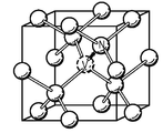
Figure 1 shows one orientation of the NV center in the diamond lattice.
2 is an energy level diagram showing the energy level of the spin state for the NV center.
3 is a schematic diagram showing a conventional NV center magnetic sensor system.
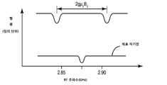
4 is a graph showing fluorescence as a function of the applied RF frequency at the NV center along a predetermined direction with respect to the zero magnetic field.
5 is a graph showing fluorescence as a function of the applied RF frequency for four different NV center orientations for a non-zero magnetic field.
6 is a schematic diagram showing a magnetic field detection system according to one embodiment.
FIG. 7 is a schematic diagram showing a Ramsey sequence of a photoexcitation pulse and an RF excitation pulse according to the operation of the system of FIG. 6; FIG.
FIG. 8A is a free induction decay curve in which the free car wash time? Is varied using the Ramsey sequence of FIG.
FIG. 8B is a magnetic measurement curve in which the RF modulation frequency? Is varied using the Ramsey sequence of FIG.
FIG. 9A is a free induction decay surface plot in which both the free car wash time? And the RF resonance frequency? Are varied using the Ramsey sequence of FIG.
FIG. 9B is a plot showing the gradient of the free induction decay surface plot of FIG. 9A. FIG.
FIG. 10 is a schematic diagram showing a Rabi sequence of a photoexcitation pulse and an RF excitation pulse according to the operation of the system of FIG. 6; FIG.
FIG. 11 is a comparison of graphs illustrating the resonant rabbit frequency according to the power of the RF excitation applied to the system of FIG. 6. FIG.
Figure 12 is a graph showing raw pulse data collected during operation of the system of Figure 6;
The present invention relates to an apparatus and method for simulating NV diamond in a magnetic detection system using an optimized simulation process to significantly increase the magnetic sensitivity of the detection system. The system utilizes a Ramsey pulse sequence to detect and measure the magnetic field acting on the system. The parameters associated with the Ramsey pulse sequence are optimized prior to measurement of the magnetic field. These parameters include the resonant rabbit frequency, the free car wash time (tau), and the tuning frequency, all of which help improve the measurement sensitivity. These parameters can be optimally determined using calibration tests utilizing other optical detection techniques, such as a rabbi pulse sequence or an additional Ramsey sequence. In addition, the parameters, in particular the resonant rabbit frequency, can be further optimized by the power increase of the RF exciters that can be achieved through the use of small loop antennas. During measurement of the magnetic field, the RF excitation pulses applied during the Ramsey sequence can be set to occur at a separate resonance frequency associated with different spin states (e.g., m s = +1 or m s = -1). By utilizing the individual resonance positions, the changes due to the temperature and / or strain effects of the system and the changes due to the external magnetic field can be separated to improve the accuracy of the measurement. Finally, the processing of the data obtained during the measurement is further optimized using at least two reference windows that use an average to obtain the signal. The above provides a magnetic detection system capable of improving the detection sensitivity of the magnetic field. In some embodiments, the optimized measurement process can result in a sensitivity of the magnetic detection system of about 9 nT / √Hz or less.
NV center, its electronic structure, and optical and RF interaction
The NV center in the diamond contains substituted nitrogen atoms at the lattice sites adjacent to the carbon vacancies as shown in Fig. The NV center can have four orientations, with each orientation corresponding to a different crystallographic orientation of the diamond grating.
The NV center may be in a neutral charge state or a negative charge state. Conventionally, the neutral charge state uses the nomenclature (NV 0 ) while the negative charge state uses the nomenclature (NV), which is adopted in this description.
The NV center has a number of electrons, each containing one hole electron from each vacancy to three hole electrons to each three carbon atoms adjacent to the vacancy, and a pair of electrons between the nitrogen and vacancies. The NV center in the negatively charged state also contains extra electrons.
The NV center has rotational symmetry and has a base state which is a spin triplet having a 3 A 2 symmetry with one spin state (m s = 0) and a base state as a spin triplet with two additional spin states m s = + 1, and m s = -1). In the absence of an external magnetic field, the m s = +1 energy level is offset from m s = 0 due to spin-spin interaction and the m s = +1 energy level is degenerated, that is, they have the same energy. The m s = 0 spin state energy level is divided from the m s = +1 energy level by an energy of 2.87 GHz for a zero external magnetic field.
Introducing an external magnetic field having a component along the NV axis raises the degeneration of the m s = + 1 energy level and divides the energy level (m s = + 1) by an amount (2 g B B Bz) Μ B is the Bohr magneton, and Bz is the component of the external magnetic field along the NV axis. This relationship is corrected to first order and inclusion of higher order corrections is a simple matter and will not affect the calculation and logic steps in the systems and methods described below.
NV center electronic structure may further comprise a triplet state (E 3) excitation, with the corresponding m s = 0 and s = m + 1 spin state. The optical transition between the ground state ( 3 A 2 ) and the excited triplet ( 3 E) is primarily spin conservation, meaning that the optical transition is between the initial and final states with the same spin. For the direct transition between the excited triplet (3 E) and the ground state (3 A 2), red light photons are emitted as photon energy corresponding to the energy difference between the energy level of the transition.
However, the middle one quartet (singlet) state (A, E) alternative non to the ground state (3 A 2) from a triplet (3 E), via an intermediate electronic state is considered to be having an intermediate energy level, - a copy decay root have. Importantly, the transition state to the excited triplet (3 E) intermediate energy level from the m s = + 1 spin state of is higher than the transition state of the m s = 0 spin state of the excited triplet (3 E) into an intermediate energy level, It is considerably larger. One transition to a neutral ground state, triplet state (3 A 2) from (A, E) is largely collapsed by m s = 0 spin state over the m = s + 1 spin states. Middle one neutral state (A, E) via excited triplet these features of the collapse of the (3 E) a ground state triplet (3 A 2) from their optical here is an optical here in the end NV center, if available to the system And allows pumping to m s = 0 spin state of base state ( 3 A 2 ). In this way, the set of m s = 0 spin states of base state 3 A 2 can be "reset" to the maximum polarization determined by the decay rate from the triplet 3 E to the medium midline state.
Another feature of the collapse, the fluorescent intensity caused by the optical stimulation to a triplet (3 E) excited state would is smaller for m = s + 1 than the m s = 0 spin state. This is so because the collapse through the intermediate state does not result in photons emitted in the fluorescent band, and that the m s = + 1 state of the excited triplet ( 3 E) state will have a greater probability of collapsing through the non- That is why. The lower fluorescence intensity for the m s = + 1 state than the m s = 0 spin state allows the fluorescence intensity to be used to determine the spin state. When the population of m s = + 1 states increases for m s = 0 spins, the overall fluorescence intensity will be reduced.
NV-centered, or self-optical defect-centered, magnetic sensor system
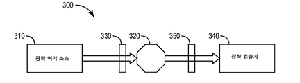
3 is m = s + a conventional magnetic sensor
The
The
For continuous wave excitation, the
Generally, the
Although FIG. 3 shows an NV centered
6 is a schematic diagram of a
The
The
The
The
The
Ramsey pulse sequence overview
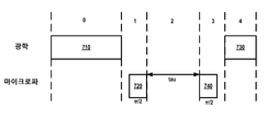
According to a particular embodiment, the
7 is a schematic diagram showing a Ramsey pulse sequence. As shown in FIG. 7, the Ramsey pulse sequence includes a photoexcitation pulse and an RF excitation pulse over a period of five stages. In a first step, during
Theoretical measurement readings from a Ramsey pulse sequence can be defined as: < RTI ID = 0.0 > (1) <
(One)
In the above equation (1), τ denotes a free precession time, T 2 * denotes spin de-pacing due to inhomogeneity in the
When measuring based on the Ramsey pulse sequence, the parameters of the duration of the MW? / 2 pulse, the frequency of the MW pulse {referred to as the amount of frequency detuned from the resonance position?), And the free wash time Lt; / RTI > 8A and 8B show the effect on the change of the specific parameter of the Ramsey pulse sequence. For example, as shown in Fig. 8A, if all the parameters are kept constant except for the free-running wash time τ, an interference pattern known as free induction decay (FID) is obtained. The FID curve is due to construction / destructive interference of three sinusoidal waves corresponding to ultrafine debris. The collapse of the signal occurs due to non-uniform de-phasing, and the rate of this collapse is represented by T 2 * (characteristic decay time). Further, as shown in FIG. 8B, if all the parameters are kept constant except for the microwave detuning (?), A magnetic field curve is obtained. In this case, the x-axis can be converted to magnetic field units through a 1 nT = 28 Hz conversion to compensate for magnetic measurements.
By changing both? and?, a two-dimensional FID surface plot can be constructed, an example of which is shown in FIG. 9A. The FID surface plot includes several characteristics that can explain the optimization of the controllable parameters of the Ramsey sequence. For example, in Figure 9A, the FID surface plot is generated using a resonance rabi frequency of about 6.25 MHz and a T 2 * of about 750 ns. The horizontal slice in FIG. 9A represents a separate FID curve (e.g., FIG. 8A), and the vertical slice represents a magnetic field curve (e.g., FIG. 8B). As shown in FIG. 9A, a higher fundamental frequency FID curve occurs in a larger detuning. Thus, higher modulation frequencies can be used to match T 2 * for diamond characterization. Further, the magnetic force measurement curve as shown in FIG. 8B shows that a specific region generates a larger sensitivity. In particular, by taking the slope of the two-dimensional FID surface plot, a separate optimal free session interval that exhibits better sensitivity can be identified, the best of which will be determined by T 2 * . Figure 9b shows the slope of the two-dimensional FID surface plot of Figure 9a. In Figure 9b, for a particular T 2 * used (i.e., about 750 ns), operating at about 900 ns (represented by
9B is characterized by T 2 *, where the attenuation of the vertical axis is characterized by the ratio of the resonant rabbit frequency ω res (described in detail below) to the effective rabbi frequency ω eff . The effective rabbit frequency can be defined by the following equation:
(2)
Thus, the ratio of the resonant rabbit frequency to the effective rabbi frequency can be expressed in terms of the resonant rabbit frequency as follows:
(3)
As shown in the above equation (3), when the resonance rabbit frequency? Res is much larger than the MW detuning?, The ratio of the resonant rabbit frequency to the effective rabbit frequency will be approximately equal to one. The attenuation shown in the vertical axis of Figure 9b can be partially controlled by the RF excitation power. As will be described in greater detail below, as the RF excitation power increases, a larger resonant rabbit frequency can be realized while reducing the rate of change of the effective rabbi frequency due to detuning. Thus, according to a particular embodiment, the magnetic force measurement is operated in a region governed by the resonant rabbit frequency to achieve maximum contrast (the ratio of (3) is close to 1).
Measurement sequence
Using the above observations, a very sensitive magnetic force measurement can generally be obtained using a three-step approach. In this general approach, a first step is performed to verify the resonance rabbit frequency? Res . The second step measures the inhomogeneous de-phasing (T 2 * ) of the system. Finally, using the measurements obtained in the first and second steps, the parameter space of equation (1) is optimized and high sensitivity magnetic measurements are performed. These three steps are described in detail below.
Measurement of resonance ravi frequency
To verify the resonant rabbit frequency, a bias magnetic field using a
After application of the rabie pulse, the resonance ravi frequency (? Res ) is defined by the frequency of the resultant curve. Figure 11 shows a measured curve AD after application of a rabbi pulse using variable RF excitation power (e.g., MW power). By increasing the MW power applied to the
T2 * Measurement of
In the second stage of the measurement process, a measurement of the inhomogeneous diphase T 2 * of the system is obtained using the π / 2 pulse determined by the resonance rabbit frequency and the resonance position obtained in the first stage above. The measurement is performed similarly to the rabbi measurement described above, except that the Ramsey pulse sequence is used. As described above with reference to the Ramsey pulse sequence, tau (tau) represents the free wash time interval at this stage.
When estimating T 2 * , the modulation frequency? Is set relatively high in certain embodiments. As described above, a large modulation frequency causes a higher fundamental frequency (see, for example, FIG. 9A) and allows a larger contrast, making it easier to tailor the data. In some embodiments, the modulation frequency? May be set at about 10 MHz. However, in the case of a relatively large T 2 * , a smaller modulation frequency can be used. FIG. 8A shows an example of a FID curve that can be used to obtain T 2 * with a modulation frequency set at about 10 MHz. By determining T 2 * from the FID curve as shown in Fig. 8A, the optimum free time of relaxation time τ can be determined based on the strong interference region described above with reference to Fig. 9B. Also, in a particular embodiment, a small range of τ is collected on both sides of the optimal freeze time determined optimally for the setter of equation (1).
Magnetic force measurement
The measurement of the fluorescence intensity response at the end of the measurement process is performed using the parameters obtained in the above step. As noted above, the identified resonance rabbit frequency provides the duration of the MW? / 2 pulse (used as the
Also, in order to increase the sensitivity, in some embodiments the second measurement made per fixed measurement error can be increased. Thus, in order to maximize sensitivity, the overall length of a single measurement cycle must be minimized, which can be achieved through the use of a higher light output of the
In conventional measurement processes, the curve of the intensity response is generally measured only once to obtain the tilt and the fine tuning frequency, while the additional measurement is performed only at the optimum tuning frequency while the fluorescence signal is being monitored. However, the system may experience drift caused by, for example, optical excitation heating (e.g., laser induced heating) and / or variations that can contribute to inaccuracies and errors during the measurement process. Tracking a single-spin resonance does not adequately account for the conversion in the response curve due to thermal effects. Thus, in accordance with some embodiments, the data obtained from the measurement process is stored in real time and the sensitivity is determined off-line to minimize the time between measurements, in order to account for non-linearity for a band of larger magnetic fields. Also, the magnetic measurement curves are collected in both m s = +1 and m s = -1 spin states for the same NV symmetry axis. For example, each in a particular embodiment, Ramsey sequence for RF excitation pulse is low resonant (i.e., m = s -1 resonance frequency of the spin state) and a high resonance (that is, m = s resonant frequency of + 1) The spin state is used to obtain measurements related to spin states (m s = -1 and m s = 1 spin states). Thus, for two positive and negative spin states, two magnetization curves (e.g., Fig. 8B) can be obtained. By applying RF pulses at discrete frequencies it is possible to compensate for deformations due to temperature and / or strain effects. The magnetic field measurements can be made using the following equations (4) and (5), where I represents the normalized intensity of the fluorescence (e.g. red) and m 1 and m 2 are the Represents the measurement taken for each of m s = +1 and m s = -1:
(4)
(5)
For the measurement obtained at the opposite slope, a positive value is used in the equation (5). m s = +1 and m s = -1 If the peak of the spin state is transformed, the magnitude response occurs in the opposite direction. On the other hand, if the peaks are separated outward due to a change in the magnetic field, the intensity change agrees to yield an appropriate dB measurement value. Thus, by obtaining a measurement of the curve for both m s = +1 and m s = -1 spin states for the same NV symmetry axis, the changes due to changes due to temperature and magnetic field can be separated. Therefore, translational movement due to temperature and / or strain effects can be considered, so that the magnetic field contribution on the system can be calculated more accurately.
Signal processing
The processing can be performed on the raw data obtained to obtain a clean image of the measurements obtained during each of the above steps. FIG. Figure 12 shows an example of a raw pulse data segment that can be obtained for a given measurement cycle. Theoretically, the signal is defined as the first 300ns of the photoexcitation pulse. However, this definition applies to the light output density in a nearly saturated state. As the optical power density decreases in the saturated state, useful portions of the signal can be further extended. At present, in the conventional processing method, when the system is polarized, the end of the pulse is referred to to explain the power fluctuation in the optical excitation source (for example, laser). This is shown in FIG. 12, where the signal is acquired using a signal window or period defined by a first reference window or period defined by C, i.e., B (i.e., signal = CB) referenced after the MW pulse . However, in accordance with certain embodiments, to increase sensitivity, the reference is a microwave pulse (i.e., signal =
The foregoing description of exemplary embodiments has been presented for purposes of illustration and description. And is not intended to be exhaustive or limited with respect to the precise form disclosed, and variations and modifications may be made in light of the above teachings, or may be acquired from practice of the disclosed embodiments. The scope of the present invention should be determined by the appended claims and their equivalents.
Claims (36)
A nitrogen vacancy (NV) diamond material comprising a plurality of NV centers;
A radio frequency (RF) excitation source configured to provide RF excitation to the NV diamond material;
An optical excitation source configured to provide an optical excitation to the NV diamond material;
An optical detector configured to receive an optical signal emitted by the NV diamond material;
A magnetic field generator configured to generate a magnetic field applied to the NV diamond material; And
Controlling the optical excitation source and the RF excitation source to apply to the NV diamond material a first pulse sequence comprising two optical excitation pulses and two RF excitation pulses;
Receiving a first photodetection signal from the optical detector based on an optical signal emitted by the NV diamond material due to the first pulse sequence;
Measuring a first value of the first photodetection signal in a first reference period prior to a period of the first photodetection signal associated with two RF excitation pulses of the first pulse sequence provided to the NV diamond material ;
Measuring a second value of the first optical detection signal in a second reference period after the period of the first optical detection signal associated with two RF excitation pulses of the first pulse sequence provided to the NV diamond material;
Calculate a first measurement based on the measured first and second values of the first photodetection signal;
Controlling the optical excitation source and the RF excitation source to apply a second pulse sequence comprising two optical excitation pulses and two RF excitation pulses to the NV diamond material;
Receiving a second photodetection signal from the optical detector based on the optical signal emitted by the NV diamond material due to the second pulse sequence;
Measuring a first value of the second photodetection signal in a first reference period prior to a period of the second photodetection signal associated with two RF excitation pulses of the second pulse sequence provided to the NV diamond material;
Measuring a second value of the second photodetection signal in a second reference period after a period of the second photodetection signal associated with two RF excitation pulses of the second pulse sequence provided to the NV diamond material;
The controller configured to calculate a second measurement based on the measured first and second values of the second optical detection signal,
Wherein the first measurement is based on a high resonant frequency of the NV diamond material,
Wherein the second measurement is based on a low resonant frequency of the NV diamond material.
A nitrogen vacancy (NV) diamond material comprising a plurality of NV centers;
A radio frequency (RF) excitation source configured to provide RF excitation to the NV diamond material;
An optical excitation source configured to provide an optical excitation to the NV diamond material;
An optical detector configured to receive an optical signal emitted by the NV diamond material;
A magnetic field generator configured to generate a magnetic field applied to the NV diamond material; And
The controller controlling the optical excitation source and the RF excitation source to apply to the NV diamond material a pulse sequence comprising two optical excitation pulses and two RF excitation pulses;
Receiving an optical detection signal from the optical detector based on the optical signal emitted by the NV diamond material due to the pulse sequence;
Measuring a first value of the photodetection signal in a first reference period prior to a period of the photodetection signal associated with the two RF excitation pulses provided to the NV diamond material;
Measuring a second value of the photodetection signal in a second reference period after the period of the photodetection signal associated with the two RF excitation pulses provided to the NV diamond material;
And the controller configured to calculate a measurement signal based on the measured first and second values.
A system for magnetic detection.
A nitrogen vacancy (NV) diamond material comprising a plurality of NV centers;
A radio frequency (RF) excitation source configured to provide RF excitation to the NV diamond material;
An optical excitation source configured to provide an optical excitation to the NV diamond material;
An optical detector configured to receive an optical signal emitted by the NV diamond material;
A magnetic field generator configured to generate a magnetic field applied to the NV diamond material; And
Controlling the optical excitation source and the RF excitation source to apply to the NV diamond material a first pulse sequence comprising two optical excitation pulses and two RF excitation pulses;
Receiving a first photodetection signal from the optical detector based on an optical signal emitted by the NV diamond material due to the first pulse sequence;
Calculate a first measurement value based on the first photo detection signal;
Controlling the optical excitation source and the RF excitation source to apply a second pulse sequence comprising two optical excitation pulses and two RF excitation pulses to the NV diamond material;
Receiving a second photodetection signal from the optical detector based on the optical signal emitted by the NV diamond material due to the second pulse sequence;
And the controller configured to calculate a second measurement based on the second photo detection signal,
Wherein the first measurement is based on a high resonant frequency of the NV diamond material,
Wherein the second measurement is based on a low resonant frequency of the NV diamond material.
A nitrogen vacancy (NV) diamond material comprising a plurality of NV centers;
A radio frequency (RF) excitation source configured to provide RF excitation to the NV diamond material;
An optical excitation source configured to provide an optical excitation to the NV diamond material;
An optical detector configured to receive an optical signal emitted by the NV diamond material;
A magnetic field generator configured to generate a magnetic field applied to the NV diamond material; And
The controller controlling the optical excitation source and the RF excitation source to apply a plurality of pulse sequences to the NV diamond material, each of the plurality of pulse sequences comprising two optical excitation pulses and an RF excitation pulse, The time period of application of the RF excitation pulse is variable between each of the plurality of pulse sequences;
Receive a plurality of optical detection signals from the optical detector based on optical signals emitted by the NV diamond material due to the plurality of pulse sequences;
Measuring a respective first value of the plurality of photodetection signals in a first reference period prior to a period associated with each RF excitation pulse of the plurality of pulse sequences;
Measuring a respective second value of the plurality of photodetection signals in a second reference period after the period associated with each RF excitation pulse of the plurality of pulse sequences;
Calculate a plurality of measurement signals based on the plurality of measured first and second values;
And the controller configured to calculate a frequency of the plurality of measurement signals.
A system for magnetic detection.
A nitrogen vacancy (NV) diamond material comprising a plurality of NV centers;
A radio frequency (RF) excitation source configured to provide RF excitation to the NV diamond material;
An optical excitation source configured to provide an optical excitation to the NV diamond material;
An optical detector configured to receive an optical signal emitted by the NV diamond material;
A magnetic field generator configured to generate a magnetic field applied to the NV diamond material; And
The controller controlling the optical excitation source and the RF excitation source to apply a plurality of pulse sequences to the NV diamond material, each of the plurality of pulse sequences comprising two optical excitation pulses and two RF excitation pulses , The time period between the application of the two RF excitation pulses being variable between each of the plurality of pulse sequences;
Receive a plurality of optical detection signals from the optical detector based on optical signals emitted by the NV diamond material due to the plurality of pulse sequences;
Measuring a respective first value of the plurality of photodetection signals in a first reference period prior to a period associated with each of the plurality of pulse sequences of the RF excitation pulse;
Measuring a respective second value of the plurality of photodetection signals in a second reference period after the period associated with each of the RF excitation pulses of the plurality of pulse sequences;
Calculate a plurality of measurement signals based on the plurality of measured first and second values;
And the controller configured to calculate a decay time of the plurality of measurement signals.
A system for magnetic detection.
Means for providing RF excitation to the NV diamond material;
Means for providing optical excitation to an NV diamond material;
Means for receiving an optical signal emitted by the NV diamond material;
Means for generating a magnetic field applied to the NV diamond material;
Means for applying to the NV diamond material a pulse sequence comprising two optical excitation pulses and two RF excitation pulses;
Means for receiving an optical detection signal based on an optical signal emitted by the NV diamond material due to the pulse sequence;
Means for measuring a first value of the photodetection signal in a first reference period prior to a period of the photodetection signal associated with the two RF excitation pulses provided to the NV diamond material;
Means for measuring a second value of the photodetection signal in a second reference period after the period of the photodetection signal associated with the two RF excitation pulses provided to the NV diamond material; And
And means for calculating a measurement signal based on the measured first and second values.
Controlling an optical excitation source and an RF excitation source to apply a pulse sequence comprising two optical excitation pulses and two RF excitation pulses to the NV diamond material;
Receiving an optical detection signal from the optical detector based on the optical signal emitted by the NV diamond material due to the pulse sequence;
Measuring a first value of the photodetection signal in a first reference period prior to a period of the photodetection signal associated with the two RF excitation pulses provided to the NV diamond material;
Measuring a second value of the photodetection signal in a second reference period after the period of the photodetection signal associated with the two RF excitation pulses of the pulse sequence provided to the NV diamond material;
And calculating a measurement signal based on the measured first and second values.
A self-defecting core material comprising a plurality of self-defect centers;
A radio frequency (RF) excitation source configured to provide RF excitation to the self-deficient center material;
An optical excitation source configured to provide optical excitation to the self-deficient center material;
An optical detector configured to receive an optical signal emitted by the self-defective center material;
A magnetic field generator configured to generate a magnetic field applied to the self-deficient central material; And
Controlling, as a controller, the optical excitation source and the RF excitation source to apply a pulse sequence comprising two optical excitation pulses and two RF excitation pulses to the magnetically-deficient center material;
Receiving an optical detection signal from the optical detector based on an optical signal emitted by the self-defocusing center material due to the pulse sequence;
Measuring a first value of the photodetection signal in a first reference period prior to a period of the photodetection signal associated with the two RF excitation pulses provided to the magnetically-deficient core material;
Measuring a second value of the photodetection signal in a second reference period after the period of the photodetection signal associated with the two RF excitation pulses provided to the magnetically-deficient core material;
And the controller configured to calculate a measurement signal based on the measured first and second values.
A system for magnetic detection.
Means for providing RF excitation to the NV diamond material;
Means for providing optical excitation to an NV diamond material;
Means for receiving an optical signal emitted by the NV diamond material;
Means for generating a magnetic field applied to the NV diamond material;
Means for applying to the NV diamond material a first pulse sequence comprising two optical excitation pulses and two RF excitation pulses;
Means for receiving a first photodetection signal based on an optical signal emitted by the NV diamond material due to the first pulse sequence;
Means for calculating a first measurement value based on the first light detection signal;
Means for applying to the NV diamond material a second pulse sequence comprising two optical excitation pulses and two RF excitation pulses;
Means for receiving a second photodetection signal based on an optical signal emitted by the NV diamond material due to the second pulse sequence; And
And means for calculating a second measurement value based on the second light detection signal,
Wherein the first measurement is based on a high resonant frequency of the NV diamond material,
Wherein the second measurement is based on a low resonant frequency of the NV diamond material.
Controlling an optical excitation source and an RF excitation source to apply a first pulse sequence comprising two optical excitation pulses and two RF excitation pulses to the NV diamond material;
Receiving a first photodetection signal from the optical detector based on the optical signal emitted by the NV diamond material due to the first pulse sequence;
Calculating a first measurement value based on the first detection signal;
Controlling the optical excitation source and the RF excitation source to apply a second pulse sequence comprising two optical excitation pulses and two RF excitation pulses to the NV diamond material;
Receiving a second photodetection signal from the optical detector based on the optical signal emitted by the NV diamond material due to the second pulse sequence; And
And calculating a second measurement value based on the second detection signal,
Wherein the first measurement is based on a high resonant frequency of the NV diamond material,
Wherein the second measurement is based on a low resonant frequency of the NV diamond material.
A self-defecting core material comprising a plurality of self-defect centers;
A radio frequency (RF) excitation source configured to provide an RF excitation to the self-deficient center material;
An optical excitation source configured to provide an optical excitation to the self-deficient center material;
An optical detector configured to receive an optical signal emitted by the self-defective center material;
A magnetic field generator configured to generate a magnetic field applied to the self-deficient central material; And
Controlling the optical excitation source and the RF excitation source to apply a first pulse sequence comprising two optical excitation pulses and two RF excitation pulses to the magnetically-deficient center material;
Receiving a first light detection signal from the optical detector based on the optical signal emitted by the self-defocusing center material due to the first pulse sequence;
Calculate a first measurement value based on the first photo detection signal;
Controlling the optical excitation source and the RF excitation source to apply a second pulse sequence comprising two optical excitation pulses and two RF excitation pulses to the self-deficient center material;
Receiving a second light detection signal from the optical detector based on the optical signal emitted by the self-defocusing center material due to the second pulse sequence;
And the controller configured to calculate a second measurement based on the second photo detection signal,
Wherein the first measurement is based on a high resonant frequency of the self-
Wherein the second measurement is based on a low resonant frequency of the self-defective center material.
Applications Claiming Priority (5)
| Application Number | Priority Date | Filing Date | Title |
|---|---|---|---|
| US201562107289P | 2015-01-23 | 2015-01-23 | |
| US62/107,289 | 2015-01-23 | ||
| US15/003,590 | 2016-01-21 | ||
| PCT/US2016/014336 WO2016118756A1 (en) | 2015-01-23 | 2016-01-21 | Apparatus and method for high sensitivity magnetometry measurement and signal processing in a magnetic detection system |
| US15/003,590 US9557391B2 (en) | 2015-01-23 | 2016-01-21 | Apparatus and method for high sensitivity magnetometry measurement and signal processing in a magnetic detection system |
Publications (1)
| Publication Number | Publication Date |
|---|---|
| KR20170108055A true KR20170108055A (en) | 2017-09-26 |
Family
ID=56417749
Family Applications (1)
| Application Number | Title | Priority Date | Filing Date |
|---|---|---|---|
| KR1020177023231A KR20170108055A (en) | 2015-01-23 | 2016-01-21 | Apparatus and method for high-sensitivity magnetic force measurement and signal processing in a magnetic detection system |
Country Status (3)
| Country | Link |
|---|---|
| US (2) | US9557391B2 (en) |
| KR (1) | KR20170108055A (en) |
| WO (1) | WO2016118756A1 (en) |
Cited By (2)
| Publication number | Priority date | Publication date | Assignee | Title |
|---|---|---|---|---|
| KR20210075402A (en) * | 2019-12-13 | 2021-06-23 | 한국표준과학연구원 | Diamond nitrogen vacancy center magnetic field sensor |
| KR20230064877A (en) * | 2021-11-04 | 2023-05-11 | 한국표준과학연구원 | Method and appratus for sensing magnetic fields or temperature of wide areas using diamond nitrogen vacancy sensor |
Families Citing this family (73)
| Publication number | Priority date | Publication date | Assignee | Title |
|---|---|---|---|---|
| US10120039B2 (en) | 2015-11-20 | 2018-11-06 | Lockheed Martin Corporation | Apparatus and method for closed loop processing for a magnetic detection system |
| US9638821B2 (en) | 2014-03-20 | 2017-05-02 | Lockheed Martin Corporation | Mapping and monitoring of hydraulic fractures using vector magnetometers |
| US10168393B2 (en) | 2014-09-25 | 2019-01-01 | Lockheed Martin Corporation | Micro-vacancy center device |
| US10006973B2 (en) | 2016-01-21 | 2018-06-26 | Lockheed Martin Corporation | Magnetometer with a light emitting diode |
| US10088336B2 (en) | 2016-01-21 | 2018-10-02 | Lockheed Martin Corporation | Diamond nitrogen vacancy sensed ferro-fluid hydrophone |
| US10088452B2 (en) | 2016-01-12 | 2018-10-02 | Lockheed Martin Corporation | Method for detecting defects in conductive materials based on differences in magnetic field characteristics measured along the conductive materials |
| US10338162B2 (en) | 2016-01-21 | 2019-07-02 | Lockheed Martin Corporation | AC vector magnetic anomaly detection with diamond nitrogen vacancies |
| US9853837B2 (en) | 2014-04-07 | 2017-12-26 | Lockheed Martin Corporation | High bit-rate magnetic communication |
| US9824597B2 (en) | 2015-01-28 | 2017-11-21 | Lockheed Martin Corporation | Magnetic navigation methods and systems utilizing power grid and communication network |
| US9910104B2 (en) | 2015-01-23 | 2018-03-06 | Lockheed Martin Corporation | DNV magnetic field detector |
| US9614589B1 (en) | 2015-12-01 | 2017-04-04 | Lockheed Martin Corporation | Communication via a magnio |
| US10241158B2 (en) | 2015-02-04 | 2019-03-26 | Lockheed Martin Corporation | Apparatus and method for estimating absolute axes' orientations for a magnetic detection system |
| US9910105B2 (en) | 2014-03-20 | 2018-03-06 | Lockheed Martin Corporation | DNV magnetic field detector |
| US10520558B2 (en) | 2016-01-21 | 2019-12-31 | Lockheed Martin Corporation | Diamond nitrogen vacancy sensor with nitrogen-vacancy center diamond located between dual RF sources |
| CA2945016A1 (en) | 2014-04-07 | 2015-10-15 | Lockheed Martin Corporation | Energy efficient controlled magnetic field generator circuit |
| WO2016118756A1 (en) | 2015-01-23 | 2016-07-28 | Lockheed Martin Corporation | Apparatus and method for high sensitivity magnetometry measurement and signal processing in a magnetic detection system |
| EP3251193A4 (en) | 2015-01-28 | 2018-08-08 | Lockheed Martin Corporation | In-situ power charging |
| WO2016126436A1 (en) | 2015-02-04 | 2016-08-11 | Lockheed Martin Corporation | Apparatus and method for recovery of three dimensional magnetic field from a magnetic detection system |
| WO2017078766A1 (en) | 2015-11-04 | 2017-05-11 | Lockheed Martin Corporation | Magnetic band-pass filter |
| WO2017087014A1 (en) | 2015-11-20 | 2017-05-26 | Lockheed Martin Corporation | Apparatus and method for hypersensitivity detection of magnetic field |
| WO2017127095A1 (en) | 2016-01-21 | 2017-07-27 | Lockheed Martin Corporation | Diamond nitrogen vacancy sensor with common rf and magnetic fields generator |
| WO2017127081A1 (en) | 2016-01-21 | 2017-07-27 | Lockheed Martin Corporation | Diamond nitrogen vacancy sensor with circuitry on diamond |
| WO2017127090A1 (en) | 2016-01-21 | 2017-07-27 | Lockheed Martin Corporation | Higher magnetic sensitivity through fluorescence manipulation by phonon spectrum control |
| GB2562957A (en) | 2016-01-21 | 2018-11-28 | Lockheed Corp | Magnetometer with light pipe |
| CA3051811A1 (en) | 2016-04-08 | 2017-10-12 | Socpra Sciences Et Genie S.E.C. | Vectorial magnetometer and associated methods for sensing an amplitude and orientation of a magnetic field |
| US10359479B2 (en) | 2017-02-20 | 2019-07-23 | Lockheed Martin Corporation | Efficient thermal drift compensation in DNV vector magnetometry |
| US10274550B2 (en) | 2017-03-24 | 2019-04-30 | Lockheed Martin Corporation | High speed sequential cancellation for pulsed mode |
| US10345395B2 (en) | 2016-12-12 | 2019-07-09 | Lockheed Martin Corporation | Vector magnetometry localization of subsurface liquids |
| US10145910B2 (en) | 2017-03-24 | 2018-12-04 | Lockheed Martin Corporation | Photodetector circuit saturation mitigation for magneto-optical high intensity pulses |
| US10345396B2 (en) | 2016-05-31 | 2019-07-09 | Lockheed Martin Corporation | Selected volume continuous illumination magnetometer |
| US10330744B2 (en) | 2017-03-24 | 2019-06-25 | Lockheed Martin Corporation | Magnetometer with a waveguide |
| US10281550B2 (en) | 2016-11-14 | 2019-05-07 | Lockheed Martin Corporation | Spin relaxometry based molecular sequencing |
| US10371765B2 (en) | 2016-07-11 | 2019-08-06 | Lockheed Martin Corporation | Geolocation of magnetic sources using vector magnetometer sensors |
| US10228429B2 (en) | 2017-03-24 | 2019-03-12 | Lockheed Martin Corporation | Apparatus and method for resonance magneto-optical defect center material pulsed mode referencing |
| US10571530B2 (en) | 2016-05-31 | 2020-02-25 | Lockheed Martin Corporation | Buoy array of magnetometers |
| US10317279B2 (en) | 2016-05-31 | 2019-06-11 | Lockheed Martin Corporation | Optical filtration system for diamond material with nitrogen vacancy centers |
| US10338163B2 (en) | 2016-07-11 | 2019-07-02 | Lockheed Martin Corporation | Multi-frequency excitation schemes for high sensitivity magnetometry measurement with drift error compensation |
| US10527746B2 (en) | 2016-05-31 | 2020-01-07 | Lockheed Martin Corporation | Array of UAVS with magnetometers |
| US10677953B2 (en) | 2016-05-31 | 2020-06-09 | Lockheed Martin Corporation | Magneto-optical detecting apparatus and methods |
| US10408890B2 (en) | 2017-03-24 | 2019-09-10 | Lockheed Martin Corporation | Pulsed RF methods for optimization of CW measurements |
| US20170343621A1 (en) | 2016-05-31 | 2017-11-30 | Lockheed Martin Corporation | Magneto-optical defect center magnetometer |
| EP3373023B1 (en) | 2017-03-06 | 2020-05-06 | Fraunhofer-Gesellschaft zur Förderung der angewandten Forschung e.V. | Sensor and method for its production and application |
| EP3376245A1 (en) * | 2017-03-16 | 2018-09-19 | ETH Zurich | Scanning sensor comprising a spin defect |
| US10459041B2 (en) | 2017-03-24 | 2019-10-29 | Lockheed Martin Corporation | Magnetic detection system with highly integrated diamond nitrogen vacancy sensor |
| WO2018174905A1 (en) * | 2017-03-24 | 2018-09-27 | Lockheed Martin Corporation | High speed sequential cancellation for pulsed mode |
| US10371760B2 (en) | 2017-03-24 | 2019-08-06 | Lockheed Martin Corporation | Standing-wave radio frequency exciter |
| WO2018174904A1 (en) * | 2017-03-24 | 2018-09-27 | Lockheed Martin Corporation | Pulsed rf methods for optimization of cw measurements |
| WO2018174914A1 (en) * | 2017-03-24 | 2018-09-27 | Lockheed Martin Corporation | Vacancy center material with highly efficient rf excitation |
| US10379174B2 (en) | 2017-03-24 | 2019-08-13 | Lockheed Martin Corporation | Bias magnet array for magnetometer |
| WO2018174906A1 (en) * | 2017-03-24 | 2018-09-27 | Lockheed Martin Corporation | Photodetector circuit saturation mitigation for magneto-optical high intensity pulses |
| US10338164B2 (en) | 2017-03-24 | 2019-07-02 | Lockheed Martin Corporation | Vacancy center material with highly efficient RF excitation |
| WO2018174907A1 (en) * | 2017-03-24 | 2018-09-27 | Lockheed Martin Corporation | Apparatus and method for resonance magneto-optical defect center material pulsed mode referencing |
| WO2018174913A1 (en) * | 2017-03-24 | 2018-09-27 | Lockheed Martin Corporation | Magneto-optical defect center material holder |
| US11340320B2 (en) * | 2017-06-29 | 2022-05-24 | Danmarks Tekniske Universitet | Magnetometer for measuring an unknown external magnetic field |
| WO2019014198A2 (en) * | 2017-07-11 | 2019-01-17 | Lockheed Martin Corporation | Phase shifted magnetometry adaptive cancellation |
| US10935611B2 (en) * | 2017-07-11 | 2021-03-02 | Lockheed Martin Corporation | Magnetometer apparatus |
| US10606271B2 (en) | 2017-07-17 | 2020-03-31 | The Boeing Company | Magnetic navigation and positioning system |
| WO2019108781A1 (en) * | 2017-11-29 | 2019-06-06 | Massachusetts Institute Of Technology | Stationary magic angle spinning enhanced solid-state spin sensor |
| JP6795803B2 (en) * | 2018-03-02 | 2020-12-02 | 国立大学法人京都大学 | Sensor elements, measuring devices, manufacturing methods of sensor elements, electronic circuit elements, and quantum information elements |
| US11187765B2 (en) * | 2018-09-18 | 2021-11-30 | Lockheed Martin Corporation | Apparatus and method for lower magnetometer drift with increased accuracy |
| US10564231B1 (en) * | 2019-01-08 | 2020-02-18 | Lockheed Martin Corporation | RF windowing for magnetometry |
| CN110095492B (en) * | 2019-04-18 | 2023-03-24 | 国仪量子(合肥)技术有限公司 | Magnetic field automatic adjusting method, computer equipment and medium |
| WO2021013308A1 (en) | 2019-07-25 | 2021-01-28 | Jan Meijer | Nv-centre-based microwave-free quantum sensor and uses and characteristics thereof |
| WO2021067587A1 (en) | 2019-10-02 | 2021-04-08 | X Development Llc | Magnetometry based on electron spin defects |
| DE102021101575A1 (en) | 2020-01-30 | 2021-08-05 | Elmos Semiconductor Se | Process for the production of an optical system with NV centers by means of optically transparent film structures |
| WO2022056232A1 (en) | 2020-09-10 | 2022-03-17 | X Development Llc | Magnetometry based on electron spin defects |
| CN112327226B (en) * | 2020-11-05 | 2024-03-19 | 北京卫星环境工程研究所 | Microwave noise elimination method based on diamond NV color center magnetic field measurement |
| US11531073B2 (en) | 2020-12-31 | 2022-12-20 | X Development Llc | Fiber-coupled spin defect magnetometry |
| CN114764131A (en) * | 2021-01-13 | 2022-07-19 | 国仪量子(合肥)技术有限公司 | Magnetic field measurement system, method, and storage medium |
| US11774384B2 (en) | 2021-01-15 | 2023-10-03 | X Development Llc | Spin defect magnetometry pixel array |
| CN114137304A (en) * | 2021-11-19 | 2022-03-04 | 中北大学 | Frequency measurement system and method of radio frequency signal |
| CN113804941B (en) * | 2021-11-22 | 2022-08-16 | 安徽省国盛量子科技有限公司 | Current measuring device and method based on diamond NV color center |
| CN116859300B (en) * | 2023-09-01 | 2023-11-17 | 华中科技大学 | Quantum sensing frequency tracking control method and system based on diamond NV color center |
Family Cites Families (456)
| Publication number | Priority date | Publication date | Assignee | Title |
|---|---|---|---|---|
| US2746027A (en) | 1951-11-16 | 1956-05-15 | James J Murray | Flux-gap variation transducer for hydrophones, microphones, and accelerometers |
| US3389333A (en) | 1964-02-10 | 1968-06-18 | Sperry Rand Corp | Control system for maintaining a desired magnetic field in a given space |
| US3359812A (en) | 1964-03-13 | 1967-12-26 | Spectra Physics | Angle adjusting mechanism for optical elements |
| US3514723A (en) | 1966-06-23 | 1970-05-26 | Warwick Electronics Inc | Tone control circuit comprising a single potentiometer |
| US3490032A (en) | 1966-12-08 | 1970-01-13 | Gulf Research Development Co | Method and apparatus utilizing a pair of spaced magnetometers for making magnetic surveys |
| US3518531A (en) | 1968-02-23 | 1970-06-30 | Varian Associates | Transient suppressor for use in magnetometer readout circuits |
| US3621380A (en) | 1969-01-02 | 1971-11-16 | Texas Instruments Inc | Method and apparatus for seismic-magnetic prospecting |
| US3745452A (en) | 1971-02-23 | 1973-07-10 | J Osburn | Magnetic field gradient apparatus and method for detecting pipe line corrosion |
| US4047805A (en) | 1973-02-14 | 1977-09-13 | Canon Kabushiki Kaisha | Ripple-free dichroic mirrors |
| US3899758A (en) | 1974-05-01 | 1975-08-12 | Gte International Inc | Variable inductive resonant circuit arrangement having a diamagnetic core for the UHF range |
| US4078247A (en) | 1975-02-05 | 1978-03-07 | Rca Corporation | Inverter circuit control circuit for precluding simultaneous conduction of thyristors |
| US4025873A (en) | 1976-08-17 | 1977-05-24 | The United States Of America As Represented By The Secretary Of The Navy | Broadband, microwave, two-stage, stagger-tuned, field effect transistor amplifier |
| US5189368A (en) | 1976-09-24 | 1993-02-23 | Lockheed Sanders, Inc. | Magnetometer |
| US4084215A (en) | 1977-02-25 | 1978-04-11 | The United States Of America As Represented By The Secretary Of The Navy | Strobe light having reduced electromagnetic radiation |
| US4329173A (en) | 1980-03-31 | 1982-05-11 | Carondelet Foundry Company | Alloy resistant to corrosion |
| US4368430A (en) | 1980-08-18 | 1983-01-11 | Sanders Associates, Inc. | Fiber optic magnetic sensors |
| US4359673A (en) | 1980-08-21 | 1982-11-16 | Bross Jr Augustus T | Electromagnetically actuated linear reciprocating self-timed motor |
| DE3037305C2 (en) | 1980-10-02 | 1986-04-03 | Flowtec AG, Reinach, Basel | Arrangement for generating constant magnetic fields of alternating polarity for magnetic-inductive flow measurement |
| US4588993A (en) | 1980-11-26 | 1986-05-13 | The United States Of America As Represented By The Secretary Of The Department Of Health And Human Services | Broadband isotropic probe system for simultaneous measurement of complex E- and H-fields |
| US4322769A (en) | 1980-12-22 | 1982-03-30 | International Business Machines Corporation | Electric switch operation monitoring circuitry |
| US5245347A (en) | 1980-12-29 | 1993-09-14 | Raytheon Company | All weather tactical strike system (AWTSS) and method of operation |
| JPS57128810A (en) | 1981-02-03 | 1982-08-10 | Olympus Optical Co Ltd | Distance measuring device |
| DE3110499C2 (en) | 1981-03-18 | 1983-12-01 | Jungheinrich Unternehmensverwaltung Kg, 2000 Hamburg | Vehicle with monitoring device and braking device as a freely movable, in particular inductively guided vehicle |
| US4636612A (en) | 1983-04-19 | 1987-01-13 | Cyclomatic Industries, Inc. | Optical tracking device |
| DE3581106D1 (en) | 1984-05-17 | 1991-02-07 | Electricity Ass Services Ltd | RADIO BEARING TO LOCATE LIGHTNING. |
| US4638324A (en) | 1984-12-10 | 1987-01-20 | Hazeltine Corporation | Resistive loop angular filter |
| US5038103A (en) | 1985-04-22 | 1991-08-06 | The United States Of America As Represented By The Secretary Of The Navy | Optical fiber magnetometer |
| US4675522A (en) | 1985-10-09 | 1987-06-23 | Spectron Development Laboratories, Inc. | Fiber optic magnetic field sensor |
| GB8530930D0 (en) | 1985-12-16 | 1986-01-29 | Mansfield P | Inductive circuit arrangements |
| GB8531368D0 (en) | 1985-12-20 | 1986-02-05 | Misson P | Data transmission system |
| DE8613511U1 (en) | 1986-05-17 | 1987-10-15 | Philips Patentverwaltung Gmbh, 2000 Hamburg, De | |
| US4945305A (en) | 1986-10-09 | 1990-07-31 | Ascension Technology Corporation | Device for quantitatively measuring the relative position and orientation of two bodies in the presence of metals utilizing direct current magnetic fields |
| GB2197953B (en) | 1986-11-27 | 1990-06-06 | Plessey Co Plc | Acoustic sensor |
| US4818990A (en) | 1987-09-11 | 1989-04-04 | Fernandes Roosevelt A | Monitoring system for power lines and right-of-way using remotely piloted drone |
| US4982158A (en) | 1988-06-23 | 1991-01-01 | Electric Power Research Institute, Inc. | Method and apparatus for magnetic detection of flaws |
| CA2008009C (en) | 1989-01-20 | 1994-05-03 | Hajime Hayashi | Apparatus for measuring magnetic field |
| US5268305A (en) | 1989-06-15 | 1993-12-07 | Biocircuits Corporation | Multi-optical detection system |
| US5252912A (en) | 1989-06-28 | 1993-10-12 | William E. Merritt | System for warning aircraft pilot of potential impact with a power line and generating time-to-time impact signal |
| US4958328A (en) | 1989-07-24 | 1990-09-18 | Texaco Inc. | Marine walkaway vertical seismic profiling |
| US5019721A (en) | 1989-08-18 | 1991-05-28 | Wisconsin Alumni Research Foundation | Active superconducting devices formed of thin films |
| GB9007408D0 (en) | 1990-04-02 | 1990-05-30 | Nycomed As | Compositions |
| US5134369A (en) | 1991-03-12 | 1992-07-28 | Hughes Aircraft Company | Three axis magnetometer sensor field alignment and registration |
| US5200855A (en) | 1991-07-12 | 1993-04-06 | Optical Coating Laboratory, Inc. | Absorbing dichroic filters |
| US5301096A (en) | 1991-09-27 | 1994-04-05 | Electric Power Research Institute | Submersible contactless power delivery system |
| US5846708A (en) | 1991-11-19 | 1998-12-08 | Massachusetts Institiute Of Technology | Optical and electrical methods and apparatus for molecule detection |
| US5210650A (en) | 1992-03-31 | 1993-05-11 | Eastman Kodak Company | Compact, passively athermalized optical assembly |
| US5638472A (en) | 1993-04-01 | 1997-06-10 | Optics For Research | Optical fiber and lens assembly having a movable lens and a fixed optical fiber |
| US5568516A (en) | 1993-07-02 | 1996-10-22 | Phonic Ear Incorporated | Very low power cordless headset system |
| US5396802A (en) | 1993-08-26 | 1995-03-14 | Viatran Corporation | Differential pressure transducer utilizing a variable ferrofluid keeper as an active magnetic circuit element |
| US5425179A (en) | 1993-10-22 | 1995-06-20 | The Charles Machine Works, Inc. | Optical sensor for measuring inclination angles |
| US5761166A (en) | 1994-05-06 | 1998-06-02 | Sedlmayr; Steven R. | Method and system for simultaneous storage and/or retrieval (storval) of a plurality of data on a disk means |
| US5420549A (en) | 1994-05-13 | 1995-05-30 | The United States Of America As Represented By The Administrator Of The National Aeronautics And Space Administration | Extended linear ion trap frequency standard apparatus |
| WO1995033972A1 (en) | 1994-06-02 | 1995-12-14 | Spectra-Physics Laserplane, Inc. | Laser alignment device and method using green light |
| US5548279A (en) | 1994-07-22 | 1996-08-20 | Mcdonnell Douglas Corporation | Method and apparatus for detecting a power line |
| GB9417719D0 (en) | 1994-09-03 | 1994-10-19 | Integrated Drilling Serv Ltd | A well data telemetry system |
| US5597762A (en) | 1994-09-27 | 1997-01-28 | Nonophase Diamond Technologies, Inc. | Field-enhanced diffusion using optical activation |
| US5586069A (en) | 1994-09-30 | 1996-12-17 | Vlsi Technology, Inc. | Arithmetic logic unit with zero sum prediction |
| GB9425712D0 (en) | 1994-12-20 | 1995-02-22 | De Beers Ind Diamond | Diffractive optics |
| DE19600241C2 (en) | 1995-01-13 | 2002-08-01 | Bruker Biospin Gmbh | Method and device for finding gemstones in a surrounding substance by means of magnetic resonance |
| US8169311B1 (en) | 1999-12-15 | 2012-05-01 | Automotive Technologies International, Inc. | Wireless transmission system for vehicular component control and monitoring |
| WO1997011905A1 (en) | 1995-09-28 | 1997-04-03 | Alliedsignal Inc. | Hydrogen and moisture getter and absorber for sealed devices |
| JPH09127252A (en) | 1995-10-26 | 1997-05-16 | Kokusai Denshin Denwa Co Ltd <Kdd> | Probing system for submarine cable |
| WO1997016722A1 (en) | 1995-10-31 | 1997-05-09 | Nkk Corporation | Magnetic sensor, and magnetic flaw detection method and apparatus using the magnetic sensor |
| JPH09210687A (en) | 1996-01-31 | 1997-08-12 | Topcon Corp | Laser level |
| US5894220A (en) | 1996-02-12 | 1999-04-13 | University Of Maryland | Apparatus for microscopic imaging of electrical and magnetic properties of room-temperature objects |
| US5731996A (en) | 1996-03-05 | 1998-03-24 | Hughes Electronics | Dipole moment detector and localizer |
| US5694375A (en) | 1996-03-22 | 1997-12-02 | The United States Of America As Represented By The Secretary Of The Navy | Ultra-broadband hydrophone |
| IT1283721B1 (en) | 1996-04-05 | 1998-04-30 | Pirelli Cavi S P A Ora Pirelli | APPARATUS AND METHOD FOR HOUSING OPTICAL COMPONENTS |
| US5719497A (en) | 1996-05-09 | 1998-02-17 | The Regents Of The University Of California | Lensless Magneto-optic speed sensor |
| US6042249A (en) | 1996-07-30 | 2000-03-28 | Bayer Corporation | Illuminator optical assembly for an analytical instrument and methods of alignment and manufacture |
| US5907420A (en) | 1996-09-13 | 1999-05-25 | Lucent Technologies, Inc. | System and method for mitigating cross-saturation in optically amplified networks |
| FR2756953B1 (en) | 1996-12-10 | 1999-12-24 | Innovatron Ind Sa | PORTABLE TELEALIMENTAL OBJECT FOR CONTACTLESS COMMUNICATION WITH A TERMINAL |
| US5867514A (en) | 1997-01-09 | 1999-02-02 | Cymer, Inc. | Laser wavelength control circuit having automatic DC offset and gain adjustment |
| JP3299477B2 (en) | 1997-02-07 | 2002-07-08 | 光信 宮城 | Manufacturing method of hollow waveguide |
| US5990469A (en) | 1997-04-02 | 1999-11-23 | Gentex Corporation | Control circuit for image array sensors |
| US6124862A (en) | 1997-06-13 | 2000-09-26 | Anivision, Inc. | Method and apparatus for generating virtual views of sporting events |
| US6064210A (en) | 1997-11-14 | 2000-05-16 | Cedar Bluff Group Corporation | Retrievable resistivity logging system for use in measurement while drilling |
| US6437563B1 (en) | 1997-11-21 | 2002-08-20 | Quantum Design, Inc. | Method and apparatus for making measurements of accumulations of magnetically susceptible particles combined with analytes |
| US6144204A (en) | 1997-11-28 | 2000-11-07 | Picker Nordstar Oy | Gradient coils for magnetic resonance meeting |
| US6121053A (en) | 1997-12-10 | 2000-09-19 | Brookhaven Science Associates | Multiple protocol fluorometer and method |
| US6433944B1 (en) | 1998-09-25 | 2002-08-13 | Fuji Photo Film Co., Ltd. | Master carrier for magnetic transfer and method for transfer |
| CA2356322A1 (en) | 1998-12-23 | 2000-06-29 | Peter D. Jakab | Magnetic resonance scanner with electromagnetic position and orientation tracking device |
| US6130753A (en) | 1999-02-01 | 2000-10-10 | The United States Of America As Represented By The Secretary Of The Air Force | Laser optical density measurement system |
| US6360173B1 (en) | 1999-02-22 | 2002-03-19 | Terrescan Technologies, Inc. | Geophysical exploration system and method |
| US6262574B1 (en) | 1999-03-12 | 2001-07-17 | The United States Of America As Represented By The Secretary Of The Navy | Sensor for measuring magnetic field strength and temperature for an electric motor |
| WO2000055368A2 (en) | 1999-03-15 | 2000-09-21 | Pe Corporation (Ny) | Probe/mobility modifier complexes for multiplex nucleic acid detection |
| US6542242B1 (en) | 1999-05-10 | 2003-04-01 | University Of Washington | Mapping air contaminants using path-integrated optical remote sensing with a non-overlapping variable path length beam geometry |
| US6809829B1 (en) | 1999-05-19 | 2004-10-26 | Matsushita Electric Industrial Co., Ltd. | Method and apparatus for evaluating aberrations of optical element and method and apparatus for adjusting optical unit and lens |
| US6215303B1 (en) | 1999-06-14 | 2001-04-10 | The United States Of America As Represented By The Secretary Of The Air Force | Wire detection system |
| JP2001006233A (en) | 1999-06-18 | 2001-01-12 | Fujitsu Ltd | Optical information storage device |
| US7118657B2 (en) | 1999-06-22 | 2006-10-10 | President And Fellows Of Harvard College | Pulsed ion beam control of solid state features |
| US20050126905A1 (en) | 1999-06-22 | 2005-06-16 | President And Fellows Of Harvard College | High-precision feedback control for ion sculpting of solid state features |
| DK1135694T3 (en) | 1999-10-04 | 2004-05-03 | Qest Quantenelektronische Syst | Device for high-resolution measurement of magnetic fields |
| US6621578B1 (en) | 1999-11-26 | 2003-09-16 | Olympus Optical Co, Ltd. | Elliposometer, sample positioning mechanism, and polarization angular adjusting mechanism, used in the elliposometer |
| US7113384B2 (en) | 2000-01-27 | 2006-09-26 | Vssl Commercial, Inc. | Dynamic degaussing system |
| FR2806506B1 (en) | 2000-03-14 | 2003-07-18 | Commissariat Energie Atomique | MAGNETOMETRIC AND INCLINOMETRIC MICROSYSTEM FOR MONITORING VALUE OBJECTS |
| WO2001084661A1 (en) | 2000-05-02 | 2001-11-08 | Paratek Microwave, Inc. | Microstrip phase shifter |
| US6788722B1 (en) | 2000-07-10 | 2004-09-07 | Coherent, Inc. | High power waveguide laser |
| JP2002107285A (en) | 2000-09-29 | 2002-04-10 | Jeol Ltd | Magnetic force microscope |
| US6398155B1 (en) | 2001-01-02 | 2002-06-04 | The United States Of America As Represented By The Secretary Of The Army | Method and system for determining the pointing direction of a body in flight |
| WO2002063620A2 (en) | 2001-02-06 | 2002-08-15 | Nano-Or Technologies (Israel) Ltd. | Multiple layer optical storage device |
| US6518747B2 (en) | 2001-02-16 | 2003-02-11 | Quantum Design, Inc. | Method and apparatus for quantitative determination of accumulations of magnetic particles |
| US6686696B2 (en) | 2001-03-08 | 2004-02-03 | Genvac Aerospace Corporation | Magnetron with diamond coated cathode |
| US7035608B2 (en) | 2001-03-16 | 2006-04-25 | Aura Communications Technology, Inc. | Methods and apparatus for tuning in an inductive system |
| US7532901B1 (en) | 2001-03-16 | 2009-05-12 | Radeum, Inc. | Methods and apparatus to detect location and orientation in an inductive system |
| EP1243897B1 (en) | 2001-03-23 | 2013-12-18 | Melexis Technologies NV | Magnetic position sensor |
| US6889316B2 (en) | 2001-03-28 | 2005-05-03 | Intel Corporation | Method and apparatus for restoring registers after cancelling a multi-cycle instruction |
| US6627916B2 (en) | 2001-03-31 | 2003-09-30 | D-Wave Systems, Inc. | High sensitivity, directional DC-squid magnetometer |
| JP2002368642A (en) | 2001-06-08 | 2002-12-20 | Sony Corp | Receiver and ic |
| US6472869B1 (en) | 2001-06-18 | 2002-10-29 | United States Of America As Represented By The Secretary Of The Air Force | Diode laser-pumped magnetometer |
| JP2003006835A (en) | 2001-06-26 | 2003-01-10 | Fuji Photo Film Co Ltd | Magnetic recording medium |
| US7148683B2 (en) | 2001-10-25 | 2006-12-12 | Intematix Corporation | Detection with evanescent wave probe |
| US6653831B2 (en) | 2001-11-20 | 2003-11-25 | Gentex Corporation | Magnetometer having a dynamically adjustable bias setting and electronic vehicle compass incorporating the same |
| US7072275B2 (en) | 2001-12-04 | 2006-07-04 | Landauer, Incorporated | Optical single-bit recording and fluorescent readout utilizing aluminum oxide single crystals |
| US7161453B2 (en) | 2002-01-23 | 2007-01-09 | Stereotaxis, Inc. | Rotating and pivoting magnet for magnetic navigation |
| US7224744B2 (en) | 2002-04-22 | 2007-05-29 | Regents Of The University Of Minnesota | Space-time multipath coding schemes for wireless communication systems |
| US7251768B2 (en) | 2002-04-22 | 2007-07-31 | Regents Of The University Of Minnesota | Wireless communication system having error-control coder and linear precoder |
| US6765487B1 (en) | 2002-10-17 | 2004-07-20 | The United States Of America As Represented By The Secretary Of The Navy | Underwater detection and deterrent system |
| US7023204B2 (en) | 2002-11-18 | 2006-04-04 | International Business Machine Corporation | Magnetic imaging microscope test system and its application for characterization of read and write heads for magnetic recording |
| GB2433737B (en) | 2002-11-21 | 2007-08-15 | Element Six Ltd | Optical quality diamond material |
| US7224532B2 (en) | 2002-12-06 | 2007-05-29 | Chevron U.S.A. Inc. | Optical uses diamondoid-containing materials |
| US7010132B2 (en) | 2003-06-03 | 2006-03-07 | Unitron Hearing Ltd. | Automatic magnetic detection in hearing aids |
| US20050031840A1 (en) | 2003-08-05 | 2005-02-10 | Xerox Corporation | RF connector |
| JP2005056785A (en) | 2003-08-07 | 2005-03-03 | Matsushita Electric Ind Co Ltd | Magnetron |
| US10443139B2 (en) | 2003-09-05 | 2019-10-15 | Brilliant Light Power, Inc. | Electrical power generation systems and methods regarding same |
| US6992638B2 (en) | 2003-09-27 | 2006-01-31 | Paratek Microwave, Inc. | High gain, steerable multiple beam antenna system |
| US7400142B2 (en) | 2003-11-06 | 2008-07-15 | Stephen John Greelish | Dynamic magnetic anomaly compensation |
| GB2424132B (en) | 2003-11-18 | 2007-10-17 | Halliburton Energy Serv Inc | High-temperature memory systems |
| US7834801B2 (en) | 2003-11-25 | 2010-11-16 | Metrotech Corporation, Inc. | Sensor fusion for model-based detection in pipe and cable locator systems |
| US6992478B2 (en) | 2003-12-22 | 2006-01-31 | Cts Corporation | Combination hall effect position sensor and switch |
| US20050138330A1 (en) | 2003-12-23 | 2005-06-23 | Maxim Integrated Products, Inc. | MAXQ microcontroller |
| US7068203B2 (en) | 2003-12-31 | 2006-06-27 | Texas Instruments Incorporated | Switched-capacitor circuits with reduced finite-gain effect |
| WO2005088259A1 (en) | 2004-03-11 | 2005-09-22 | Robert Bosch Gmbh | Magnet sensor arrangement |
| WO2005096059A1 (en) | 2004-03-31 | 2005-10-13 | Olympus Corporation | Observing device and fluorescent light observing device |
| US7305869B1 (en) | 2004-04-12 | 2007-12-11 | U. S. Department Of Energy | Spin microscope based on optically detected magnetic resonance |
| US7245133B2 (en) | 2004-07-13 | 2007-07-17 | Credence Systems Corporation | Integration of photon emission microscope and focused ion beam |
| JP2006040976A (en) | 2004-07-22 | 2006-02-09 | Hamamatsu Photonics Kk | Photodetector |
| US7741936B1 (en) | 2004-09-09 | 2010-06-22 | University Of South Florida | Tunable micro electromechanical inductor |
| US7470885B2 (en) | 2004-09-13 | 2008-12-30 | Panasonic Corporation | Photodetector-amplifier circuit and optical pickup device |
| NZ535390A (en) | 2004-09-16 | 2007-10-26 | Auckland Uniservices Ltd | Inductively powered mobile sensor system |
| US7391675B2 (en) | 2004-09-17 | 2008-06-24 | Schlumberger Technology Corporation | Microseismic event detection and location by continuous map migration |
| US7543780B1 (en) | 2004-10-04 | 2009-06-09 | The United States Of America As Represented By The Secretary Of The Air Force | Unmanned air vehicle transmission line docking surveillance |
| US7307416B2 (en) | 2004-10-22 | 2007-12-11 | Delphi Technologies, Inc. | Position sensor and assembly |
| BE1016537A3 (en) | 2004-11-10 | 2007-01-09 | Wetenschappelijk En Tech Onder | METHOD FOR DISTINCTING COLORLESS AND ALMOST COLORLESS DIAMONDS AND ARRANGEMENT FOR CARRYING OUT THIS METHOD. |
| US7471805B2 (en) | 2004-12-20 | 2008-12-30 | Central Coast Patent Agency, Inc. | Hearing aid mechanism |
| US8059019B2 (en) | 2005-01-25 | 2011-11-15 | Atmel Corporation | Method and system for minimizing the accumulated offset error for an analog to digital converter |
| US20100004802A1 (en) | 2005-01-25 | 2010-01-07 | William Kress Bodin | Navigating UAVS with an on-board digital camera |
| GB2462212B (en) | 2005-02-16 | 2010-05-12 | Illinois Tool Works | Metal detector |
| EP1864082B1 (en) | 2005-03-18 | 2016-10-26 | Gatekeeper Systems, Inc. | Two-way communication system for tracking locations and statuses of wheeled vehicles |
| KR20070120105A (en) | 2005-03-18 | 2007-12-21 | 야마하하쓰도키 가부시키가이샤 | Flight control system |
| US7212351B2 (en) | 2005-04-28 | 2007-05-01 | Olympus Imaging Corp. | Zoom optical system and image taking apparatus using the same |
| JP5559448B2 (en) | 2005-05-10 | 2014-07-23 | ジーイー・メディカル・システムズ・グローバル・テクノロジー・カンパニー・エルエルシー | Magnetic resonance imaging apparatus and magnetic resonance imaging method |
| EP1891741A4 (en) | 2005-06-08 | 2011-08-24 | Powercast Corp | Powering devices using rf energy harvesting |
| US9270387B2 (en) | 2005-06-15 | 2016-02-23 | Wfs Technologies Ltd. | Mobile device with an underwater communications system and method |
| GB2428690B (en) | 2005-06-22 | 2010-12-29 | Element Six Ltd | High colour diamond |
| US7684660B2 (en) | 2005-06-24 | 2010-03-23 | Intel Corporation | Methods and apparatus to mount a waveguide to a substrate |
| JP2007099223A (en) | 2005-10-07 | 2007-04-19 | Toyota Motor Corp | Hybrid vehicle |
| US8913900B2 (en) | 2005-10-11 | 2014-12-16 | President And Fellows Of Harvard College | Method and apparatus for fault-tolerant quantum communication based on solid-state photon emitters |
| EP1952370B1 (en) | 2005-11-16 | 2010-09-01 | Koninklijke Philips Electronics N.V. | Universal rf wireless sensor interface |
| JP5005256B2 (en) | 2005-11-28 | 2012-08-22 | 株式会社日立ハイテクノロジーズ | Magnetic field measurement system and optical pumping magnetometer |
| EP1795920B1 (en) | 2005-12-09 | 2013-07-17 | Services Pétroliers Schlumberger | An electromagnetic imaging method and device |
| CN101351617A (en) | 2005-12-29 | 2009-01-21 | 尼尔·斯佩克 | Magnetic beacon guidance system |
| JP4896526B2 (en) | 2006-01-11 | 2012-03-14 | 株式会社東芝 | Magnetic resonance imaging system |
| US7448548B1 (en) | 2006-01-13 | 2008-11-11 | Point Six Wireless, Llc | Pulsed wireless directional object counter |
| US20070166730A1 (en) | 2006-01-19 | 2007-07-19 | Menon & Associates, Inc. | Magnetic resonance system and method to detect and confirm analytes |
| EP1818651A1 (en) | 2006-02-10 | 2007-08-15 | Rijksuniversiteit Groningen | System and a method for determining one or more parameters of a source of a potential-energy field |
| US7342399B1 (en) | 2006-04-17 | 2008-03-11 | The United States Of America As Represented By The Secretary Of The Navy | Magnetic anomaly sensing-based system for tracking a moving magnetic target |
| US7221164B1 (en) | 2006-04-25 | 2007-05-22 | Barringer Anthony R | Airborne remote sensing electric field exploration system |
| EP2031384A1 (en) | 2006-06-16 | 2009-03-04 | Murata Manufacturing Co. Ltd. | Sensor for detecting substance in liquid |
| US7701196B2 (en) | 2006-08-18 | 2010-04-20 | The United States Of America As Represented By The Secretary Of The Army | Methods for detecting and classifying loads on AC lines |
| US7546000B2 (en) | 2006-09-07 | 2009-06-09 | Hewlett-Packard Development Company, L.P. | Scalable and defect-tolerant color-center-based quantum computer architectures and methods for fabricating color-center-based quantum computer architectures |
| US7795997B2 (en) | 2006-09-25 | 2010-09-14 | Avago Technologies Wireless Ip (Singapore) Pte. Ltd. | Apparatus and method for measuring an environmental condition |
| JP4228020B2 (en) | 2006-09-27 | 2009-02-25 | シャープ株式会社 | Photoreceiver / amplifier circuit, optical pickup device and optical disk device |
| US8208502B2 (en) | 2006-10-03 | 2012-06-26 | California Institute Of Technology | Fiber-coupled solid state microcavity light emitters |
| US7427525B2 (en) | 2006-10-13 | 2008-09-23 | Hewlett-Packard Development Company, L.P. | Methods for coupling diamond structures to photonic devices |
| JP4800896B2 (en) | 2006-10-16 | 2011-10-26 | シャープ株式会社 | Magnetic sensor element and manufacturing method thereof, magnetic head, magnetic reproducing apparatus, and magnetic reproducing method |
| JP4978774B2 (en) | 2006-11-08 | 2012-07-18 | アイシン精機株式会社 | Mounting structure of rotation angle detector |
| US8310251B2 (en) | 2007-01-03 | 2012-11-13 | University Of Florida Research Foundation, Inc. | System for assessing pipeline condition |
| US8249689B2 (en) | 2007-02-23 | 2012-08-21 | General Electric Company | Coil arrangement for electromagnetic tracking method and system |
| US7805030B2 (en) | 2007-03-08 | 2010-09-28 | Hewlett-Packard Development Company, L.P. | Optical structures including selectively positioned color centers, photonic chips including same, and methods of fabricating optical structures |
| GB0704516D0 (en) | 2007-03-08 | 2007-04-18 | Element Six Ltd | Diamond |
| US7570358B2 (en) | 2007-03-30 | 2009-08-04 | Asml Netherlands Bv | Angularly resolved scatterometer, inspection method, lithographic apparatus, lithographic processing cell device manufacturing method and alignment sensor |
| JP4312241B2 (en) | 2007-04-12 | 2009-08-12 | 三洋電機株式会社 | Optical pickup device and optical disk device |
| US7872477B2 (en) | 2007-04-30 | 2011-01-18 | Kjt Enterprises, Inc. | Multi-component marine electromagnetic signal acquisition cable and system |
| US8026723B2 (en) | 2007-04-30 | 2011-09-27 | Kjt Enterprises, Inc. | Multi-component marine electromagnetic signal acquisition method |
| KR100885265B1 (en) | 2007-05-09 | 2009-02-23 | 강릉대학교산학협력단 | System and method for wireless communication in underwater |
| EP1990313A1 (en) | 2007-05-10 | 2008-11-12 | INSERM (Institut National de la Santé et de la Recherche Médicale) | Method to produce light-emitting nano-particles of diamond |
| US8480653B2 (en) | 2007-05-23 | 2013-07-09 | Biosense Webster, Inc. | Magnetically guided catheter with concentric needle port |
| US20080299904A1 (en) | 2007-06-04 | 2008-12-04 | Seagate Technology Llc | Wireless communication system |
| KR101335769B1 (en) | 2007-06-04 | 2013-12-02 | 엘지전자 주식회사 | Display apparatus |
| AT505470B1 (en) | 2007-06-15 | 2010-09-15 | Univ Graz Tech | METHOD AND DEVICE FOR MEASURING MAGNETIC FIELDS |
| US8129984B2 (en) | 2007-06-27 | 2012-03-06 | Brooks Automation, Inc. | Multiple dimension position sensor |
| JP5039452B2 (en) | 2007-06-27 | 2012-10-03 | 株式会社日立ハイテクノロジーズ | Magnetic field measuring device |
| KR20090004267A (en) | 2007-07-06 | 2009-01-12 | 엘지전자 주식회사 | Telematics terminal capable of receiving broadcast and method of processing broadcast signal |
| US7705599B2 (en) | 2007-07-09 | 2010-04-27 | Kjt Enterprises, Inc. | Buoy-based marine electromagnetic signal acquisition system |
| US7608820B1 (en) | 2007-08-28 | 2009-10-27 | The United States Of America As Represented By The United States Department Of Energy | Spin microscope based on optically detected magnetic resonance |
| US7667482B2 (en) | 2007-09-21 | 2010-02-23 | Eaton Corporation | Inductively powered power bus apparatus |
| US7834621B2 (en) | 2007-09-25 | 2010-11-16 | General Electric Company | Electromagnetic tracking employing scalar-magnetometer |
| FR2921260B1 (en) | 2007-09-25 | 2012-08-24 | Lesaffre & Cie | USE OF A NEW NATURAL AGENT IN COSMETIC COMPOSITIONS |
| DE202007014319U1 (en) | 2007-10-12 | 2009-02-26 | Woelke Magnetbandtechnik Gmbh & Co. Kg | Magnetic field sensitive sensor |
| US8947080B2 (en) | 2007-12-03 | 2015-02-03 | President And Fellows Of Harvard College | High sensitivity solid state magnetometer |
| FR2924826B1 (en) | 2007-12-11 | 2010-03-05 | Commissariat Energie Atomique | ATOMIC CLOCK WITH CORRECTION OF THE AMBIENT MAGNETIC FIELD |
| US7413011B1 (en) | 2007-12-26 | 2008-08-19 | Schlumberger Technology Corporation | Optical fiber system and method for wellhole sensing of magnetic permeability using diffraction effect of faraday rotator |
| BRPI0908763A2 (en) | 2008-02-07 | 2015-07-28 | Lahav Gan | Device, method for obtaining a frequency reference and system. |
| US9360844B2 (en) | 2008-02-07 | 2016-06-07 | Dimension 4 Ltd. | Apparatus, system, and method of frequency generation using an atomic resonator |
| US8064408B2 (en) | 2008-02-20 | 2011-11-22 | Hobbit Wave | Beamforming devices and methods |
| JP5169379B2 (en) | 2008-03-28 | 2013-03-27 | 富士通オプティカルコンポーネンツ株式会社 | Circuit device and circuit device apparatus |
| US20090260824A1 (en) | 2008-04-18 | 2009-10-22 | David Booth Burns | Hydrocarbon production from mines and tunnels used in treating subsurface hydrocarbon containing formations |
| GB0808856D0 (en) | 2008-05-15 | 2008-06-25 | Univ Warwick | Fabricated nanopores and micropores for chemical and biochemical analysis |
| CA2725088C (en) | 2008-05-20 | 2017-03-28 | Oxane Materials, Inc. | Method of manufacture and the use of a functional proppant for determination of subterranean fracture geometries |
| US20110066379A1 (en) | 2008-05-26 | 2011-03-17 | Mes Marius J | survey system for locating geophysical anomalies |
| AT506816B9 (en) | 2008-05-28 | 2010-01-15 | Mohaupt Peter Dipl Ing | VLF test |
| US8068571B2 (en) | 2008-06-12 | 2011-11-29 | Harris Corporation | Featureless coherent chaotic amplitude modulation |
| US8884617B2 (en) | 2008-06-23 | 2014-11-11 | The Regents Of The University Of California | Magnetic particle imaging devices and methods |
| US20100015918A1 (en) | 2008-07-18 | 2010-01-21 | Ferro Solutions, Inc. | Wireless transfer of information using magneto-electric devices |
| GB0813490D0 (en) | 2008-07-23 | 2008-08-27 | Element Six Ltd | Solid state material |
| GB0813491D0 (en) | 2008-07-23 | 2008-08-27 | Element Six Ltd | Diamond Material |
| US7983812B2 (en) | 2008-08-04 | 2011-07-19 | Scott Potter & Associates, Llc | Method and apparatus for managing battery power in emergency vehicles |
| CN102171588A (en) | 2008-08-05 | 2011-08-31 | Mr技术公司 | Differential gradiometric magnetometer, system and method of use |
| US9082673B2 (en) | 2009-10-05 | 2015-07-14 | Zena Technologies, Inc. | Passivated upstanding nanostructures and methods of making the same |
| RU2357866C1 (en) | 2008-09-10 | 2009-06-10 | Общество С Ограниченной Ответственностью "Новые Энергетические Технологии" | Method for protection of documents, securities or products with help of nanodiamonds with active nv centers |
| US9744858B2 (en) | 2008-09-27 | 2017-08-29 | Witricity Corporation | System for wireless energy distribution in a vehicle |
| US8497601B2 (en) | 2008-09-27 | 2013-07-30 | Witricity Corporation | Wireless energy transfer converters |
| US8482158B2 (en) | 2008-09-27 | 2013-07-09 | Witricity Corporation | Wireless energy transfer using variable size resonators and system monitoring |
| US20100277121A1 (en) | 2008-09-27 | 2010-11-04 | Hall Katherine L | Wireless energy transfer between a source and a vehicle |
| US8963488B2 (en) | 2008-09-27 | 2015-02-24 | Witricity Corporation | Position insensitive wireless charging |
| US8933594B2 (en) | 2008-09-27 | 2015-01-13 | Witricity Corporation | Wireless energy transfer for vehicles |
| US8901778B2 (en) | 2008-09-27 | 2014-12-02 | Witricity Corporation | Wireless energy transfer with variable size resonators for implanted medical devices |
| US8907531B2 (en) | 2008-09-27 | 2014-12-09 | Witricity Corporation | Wireless energy transfer with variable size resonators for medical applications |
| US8164340B2 (en) | 2008-10-23 | 2012-04-24 | Kjt Enterprises, Inc. | Method for determining electromagnetic survey sensor orientation |
| US8766630B2 (en) * | 2008-11-04 | 2014-07-01 | The University Of Melbourne | Method and apparatus for monitoring a property of a sample |
| US8459002B2 (en) | 2008-11-25 | 2013-06-11 | John P. McLean | Efficient RF electromagnetic propulsion system with communications capability |
| US8630584B2 (en) | 2008-11-26 | 2014-01-14 | Nationz Technologies Inc. | RF SIM card, card reader, and communication method |
| JP5558698B2 (en) | 2008-11-28 | 2014-07-23 | 株式会社東芝 | Magnetic recording head, magnetic head assembly, magnetic recording apparatus, and magnetic recording method |
| US7869047B2 (en) | 2008-12-18 | 2011-01-11 | Eastman Kodak Company | In-line self spacing optical sensor assembly for a printer |
| US7932718B1 (en) | 2009-03-12 | 2011-04-26 | The United States Of America As Represented By The Secretary Of The Navy | System and method using magnetic anomaly field magnitudes for detection, localization, classification and tracking of magnetic objects |
| US8622302B2 (en) | 2009-03-17 | 2014-01-07 | Datalogic ADC, Inc. | Systems and methods for compensating for fixed pattern noise |
| US8138756B2 (en) | 2009-04-24 | 2012-03-20 | Hewlett-Packard Development Company, L.P. | Microfiber magnetometer |
| US8134369B2 (en) | 2009-04-28 | 2012-03-13 | Kjt Enterprises, Inc. | Method of testing electric field recording of a marine electromagnetic sensor cable |
| US8477046B2 (en) | 2009-05-05 | 2013-07-02 | Advanced Technologies Group, LLC | Sports telemetry system for collecting performance metrics and data |
| US8120355B1 (en) | 2009-05-27 | 2012-02-21 | Lockheed Martin Corporation | Magnetic anomaly detector |
| US8311767B1 (en) | 2009-07-13 | 2012-11-13 | Lockheed Martin Corporation | Magnetic navigation system |
| US8334690B2 (en) | 2009-08-07 | 2012-12-18 | The United States of America as represented by the Secretary of Commerce, the National Institute of Standards and Technology | Atomic magnetometer and method of sensing magnetic fields |
| US20110127999A1 (en) | 2009-08-14 | 2011-06-02 | Paul Lott | Pipeline inspection apparatus and method |
| JP5290098B2 (en) | 2009-09-10 | 2013-09-18 | ルネサスエレクトロニクス株式会社 | Transmitter and semiconductor integrated circuit usable therefor |
| US8193808B2 (en) | 2009-09-11 | 2012-06-05 | Hewlett-Packard Development Company, L.P. | Optically integrated biosensor based on optically detected magnetic resonance |
| JP2011065702A (en) | 2009-09-16 | 2011-03-31 | Hitachi Media Electoronics Co Ltd | Optical disk apparatus |
| KR101204504B1 (en) | 2009-10-16 | 2012-11-26 | 한국과학기술원 | Method and apparatus for autonomous driving of electric vehicle |
| EP2504662B1 (en) | 2009-11-24 | 2018-11-21 | Nokia Technologies Oy | Positioning a device relative to a magnetic signal source |
| WO2011084483A2 (en) | 2009-12-16 | 2011-07-14 | Shb Instruments, Inc. | Underwater acoustic navigation systems and methods |
| US20110153339A1 (en) | 2009-12-23 | 2011-06-23 | Jonas Software | Multi-Site Club Membership |
| TW201145918A (en) | 2009-12-27 | 2011-12-16 | Maxlinear Inc | Methods and apparatus for synchronization in multiple-channel communication systems |
| TWI562554B (en) | 2009-12-30 | 2016-12-11 | Sony Corp | Communications system and device using beamforming |
| US8456159B2 (en) | 2010-01-15 | 2013-06-04 | Vale S.A. | Stabilization system for sensors on moving platforms |
| US9017633B2 (en) | 2010-01-18 | 2015-04-28 | Element Six Technologies Limited | CVD single crystal diamond material |
| JP5476206B2 (en) | 2010-02-02 | 2014-04-23 | 日本電子株式会社 | Fluorescence microscope device |
| US8294306B2 (en) | 2010-03-16 | 2012-10-23 | Indian Institute Of Technology Madras | DC capacitor balancing |
| KR101179126B1 (en) | 2010-03-31 | 2012-09-07 | 전자부품연구원 | magnetic field communication method for managing node with low power comsumption and the node operated thereby |
| US8415640B2 (en) | 2010-04-19 | 2013-04-09 | President And Fellows Of Harvard College | Diamond nanowires |
| US20110270078A1 (en) | 2010-04-30 | 2011-11-03 | Wagenaar Douglas J | Methods and systems of combining magnetic resonance and nuclear imaging |
| US8754649B2 (en) | 2010-05-12 | 2014-06-17 | Pgs Geophysical As | Electromagnetic survey systems and methods with rotation-corrected motion compensation |
| WO2011146661A2 (en) | 2010-05-19 | 2011-11-24 | Qualcomm Incorporated | Adaptive wireless energy transfer system |
| US8158277B1 (en) | 2010-09-30 | 2012-04-17 | Global Energy Science, LLC (California) | Cross-flow electrochemical batteries |
| WO2011153339A1 (en) | 2010-06-02 | 2011-12-08 | William Marsh Rice University | Magnetic particles for determining reservoir parameters |
| US9037314B2 (en) | 2010-06-21 | 2015-05-19 | Optimal Ranging, Inc. | UAV power line position and load parameter estimation |
| TWI407677B (en) | 2010-06-29 | 2013-09-01 | Univ Ishou | Power conversion device |
| GB201013112D0 (en) | 2010-08-04 | 2010-09-22 | Element Six Ltd | A diamond optical element |
| US20120037803A1 (en) | 2010-08-12 | 2012-02-16 | Flir Systems, Inc. | Electromagnetic interference shield |
| US9035626B2 (en) | 2010-08-18 | 2015-05-19 | Volterra Semiconductor Corporation | Switching circuits for extracting power from an electric power source and associated methods |
| JP5789790B2 (en) | 2010-09-10 | 2015-10-07 | パナソニックIpマネジメント株式会社 | Power transmission device and wireless power transmission system |
| GB201015260D0 (en) | 2010-09-14 | 2010-10-27 | Element Six Ltd | A microfluidic cell and a spin resonance device for use therewith |
| SE1051137A1 (en) | 2010-10-29 | 2012-04-30 | Fairchild Semiconductor | Process for manufacturing a silicon carbide bipolar transistor and silicon carbide bipolar transistor thereof |
| KR101889575B1 (en) | 2010-11-05 | 2018-08-17 | 시노케어 메디텍, 인크. | Improved algorithm for detection of diabetes |
| JP2012103171A (en) | 2010-11-11 | 2012-05-31 | Jeol Resonance Inc | Magnetic field measuring device |
| US8731360B2 (en) | 2010-11-12 | 2014-05-20 | Shenzhen University | Photonic crystal magneto-optical circulator and manufacturing method thereof |
| JP2012110489A (en) | 2010-11-24 | 2012-06-14 | Sumitomo Electric Ind Ltd | Magnetism measuring instrument, and method for manufacturing magnetism sensor element |
| US20120140219A1 (en) | 2010-12-07 | 2012-06-07 | Cleary Joseph A | Monolithic Geared Optical Reflector |
| JP2012121748A (en) | 2010-12-07 | 2012-06-28 | Sumitomo Electric Ind Ltd | Diamond and magnetic sensor using the same |
| JP5601183B2 (en) | 2010-12-07 | 2014-10-08 | 住友電気工業株式会社 | Diamond substrate and manufacturing method thereof |
| EP2652388A1 (en) | 2010-12-15 | 2013-10-23 | Illinois Tool Works, Inc. | Heat-sink/connector system for light emitting diode |
| GB201021985D0 (en) | 2010-12-24 | 2011-02-02 | Element Six Ltd | Dislocation engineering in single crystal synthetic diamond material |
| CN103339674B (en) | 2011-01-21 | 2016-03-09 | 三菱电机株式会社 | Optical take-up apparatus and optical disc apparatus |
| CN102620153A (en) | 2011-01-31 | 2012-08-01 | 旭丽电子(广州)有限公司 | Lamp |
| US8471137B2 (en) | 2011-02-22 | 2013-06-25 | Kenneth Michael ADAIR | Pickup system with a cartridge |
| EP2495166A1 (en) | 2011-03-03 | 2012-09-05 | Asociacion de la Industria Navarra (AIN) | Aerial robotic system for the inspection of overhead power lines |
| US9001003B2 (en) | 2011-03-07 | 2015-04-07 | Htc Corporation | Handheld device |
| US9442205B2 (en) | 2011-03-23 | 2016-09-13 | Global Ambient Seismic, Inc. | Method for assessing the effectiveness of modifying transmissive networks of natural reservoirs |
| JP5741115B2 (en) | 2011-03-25 | 2015-07-01 | ソニー株式会社 | POSITIONING DEVICE, POSITIONING METHOD, PROGRAM, AND RECORDING MEDIUM |
| WO2012129654A1 (en) | 2011-03-31 | 2012-10-04 | Laurentian University Of Sudbury | Multi-component electromagnetic prospecting apparatus and method of use thereof |
| WO2012149869A1 (en) | 2011-05-03 | 2012-11-08 | 国民技术股份有限公司 | Communication method, communication device and communication system |
| DK2521221T3 (en) | 2011-05-06 | 2014-07-21 | Oticon As | Receiver and method for retrieving an information signal from a magnetic induction signal |
| GB201107552D0 (en) | 2011-05-06 | 2011-06-22 | Element Six Ltd | Diamond sensors, detectors, and quantum devices |
| GB201107730D0 (en) | 2011-05-10 | 2011-06-22 | Element Six Ltd | Diamond sensors, detectors and quantum devices |
| GB201108644D0 (en) | 2011-05-24 | 2011-07-06 | Element Six Ltd | Diamond sensors, detectors, and quantum devices |
| WO2012174019A1 (en) | 2011-06-13 | 2012-12-20 | President And Fellows Of Harvard College | Absorption-based detection of spin impurities in solid-state spin systems |
| US9784804B2 (en) | 2011-06-13 | 2017-10-10 | President And Fellows Of Harvard College | Dynamic decoupling in solid state spin ensembles |
| US20140191752A1 (en) | 2011-06-13 | 2014-07-10 | President And Fellows Of Harvard College | Spectral Decomposition Of Composite Solid State Spin Environments Through Quantum Control of Spin Impurities |
| WO2012174125A1 (en) | 2011-06-13 | 2012-12-20 | President And Fellows Of Harvard College | Efficient fluorescence detection in solid state spin systems |
| US8575929B1 (en) | 2011-06-20 | 2013-11-05 | The United States Of America As Represented By The Secretary Of The Navy | Magnetic anomaly surveillance system using spherical trilateration |
| CN103814289A (en) | 2011-07-22 | 2014-05-21 | 比奥森西亚专利有限公司 | Reader device for luminescent immunoassays |
| JP5891636B2 (en) | 2011-07-28 | 2016-03-23 | 住友電気工業株式会社 | Polycrystalline diamond and method for producing the same |
| WO2013066446A1 (en) | 2011-08-01 | 2013-05-10 | The Trustees Of Columbia University In The City Of New York | Conjugates of nano-diamond and magnetic or metallic particles |
| US9929429B2 (en) | 2011-08-08 | 2018-03-27 | Battelle Memorial Institute | Polymer-sulfur composite materials for electrodes in Li-S energy storage devices |
| US8717010B2 (en) | 2011-08-19 | 2014-05-06 | Infineon Technologies Ag | Magnetic position sensors, systems and methods |
| WO2013027074A2 (en) | 2011-08-23 | 2013-02-28 | ARACONSYS Kft. | Magnetometer, method for its operation and non-destructive material testing apparatus |
| FR2979787B1 (en) | 2011-09-07 | 2013-10-11 | Commissariat Energie Atomique | PRINTED CIRCUIT AND MAGNETIC FIELD OR CURRENT SENSOR |
| WO2013040446A1 (en) | 2011-09-16 | 2013-03-21 | The Trustees Of Columbia University In The City Of New York | High-precision ghz clock generation using spin states in diamond |
| US20130070252A1 (en) | 2011-09-21 | 2013-03-21 | Honeywell International Inc. | Systems and methods for a hollow core resonant filter |
| EP2766859B1 (en) | 2011-10-14 | 2020-12-16 | Element Six Technologies Limited | Quantum processing device |
| US9194922B2 (en) | 2011-10-18 | 2015-11-24 | Technion Research & Development Foundation Limited | System and method for electron spin resonance |
| US9632045B2 (en) | 2011-10-19 | 2017-04-25 | The Trustees Of Columbia University In The City Of New York | Systems and methods for deterministic emitter switch microscopy |
| EP2769417A4 (en) | 2011-10-19 | 2015-05-27 | Univ Columbia | Systems and methods for deterministic emitter switch microscopy |
| EP2587232B1 (en) | 2011-10-27 | 2019-06-05 | Universität des Saarlandes | System and method for detecting mechanical vibrations |
| US8817254B2 (en) | 2011-10-28 | 2014-08-26 | Hewlett-Packard Development Company, L.P. | Entanglement process |
| KR20140088585A (en) | 2011-10-28 | 2014-07-10 | 휴렛-팩커드 디벨롭먼트 컴퍼니, 엘.피. | Devices including a diamond layer |
| JP5811800B2 (en) | 2011-11-18 | 2015-11-11 | 富士通株式会社 | Control circuit and electronic equipment |
| WO2013082382A1 (en) | 2011-11-30 | 2013-06-06 | President And Fellows Of Harvard College | Use of nuclear spin impurities to suppress electronic spin fluctuations and decoherence in composite solid-state spin systems |
| GB201121642D0 (en) | 2011-12-16 | 2012-01-25 | Element Six Ltd | Single crtstal cvd synthetic diamond material |
| ES2415558B1 (en) | 2011-12-23 | 2014-05-21 | Universidad De Zaragoza | DEVICE AND METHOD OF SENSATING MAGNETIC MATERIALS |
| WO2013096941A1 (en) | 2011-12-23 | 2013-06-27 | President And Fellows Of Harvard College | Solid-state quantum memory based on a nuclear spin coupled to an electronic spin |
| FI124153B (en) | 2012-01-11 | 2014-04-15 | Indooratlas Oy | Use of magnetic field-based navigation |
| US20130257419A1 (en) | 2012-03-27 | 2013-10-03 | Be Aerospace, Inc. | Magnetic encoder system for aircraft seating actuator |
| US9366735B2 (en) | 2012-04-06 | 2016-06-14 | Hitachi, Ltd. | Optical pumping magnetometer |
| WO2014011286A2 (en) | 2012-04-13 | 2014-01-16 | The Regents Of The University Of California | Gyroscopes based on nitrogen-vacancy centers in diamond |
| EP2845290B1 (en) | 2012-05-03 | 2018-08-29 | Powermat Technologies Ltd. | System and method for triggering power transfer across an inductive power coupling and non resonant transmission |
| US8849124B2 (en) | 2012-05-04 | 2014-09-30 | Raytheon BBN Technologies, Corp. | Boundless reading of information bits with a single photon |
| WO2013171544A1 (en) | 2012-05-15 | 2013-11-21 | Schlumberger Canada Limited | Nmr analysis of a core sample employing an open permanent magnet removable from a core holder |
| WO2013188651A1 (en) | 2012-06-14 | 2013-12-19 | The Trustees Of Columbia University In The City Of New York | Systems and methods for detection of electric fields, ion exchange, and ph using spectral shift in diamond color centers |
| WO2013188732A1 (en) | 2012-06-14 | 2013-12-19 | The Trustees Of Columbia University In The City Of New York | Systems and methods for precision optical imaging of electrical currents and temperature in integrated circuits |
| GB201211159D0 (en) | 2012-06-22 | 2012-08-08 | Ucl Business Plc | Electron spin resonance (ESR) analytical method and related aspects |
| US9726518B2 (en) | 2012-07-13 | 2017-08-08 | Qualcomm Incorporated | Systems, methods, and apparatus for detection of metal objects in a predetermined space |
| US20150225052A1 (en) | 2012-07-17 | 2015-08-13 | Steve Cordell | Method and Apparatus for Precision Tracking of Approaching Magnetic-Detonated and Traditional Impact Torpedoes |
| US9518821B2 (en) | 2012-08-02 | 2016-12-13 | Benjamin Malay | Vehicle control system |
| US10041971B2 (en) | 2012-08-22 | 2018-08-07 | President And Fellows Of Harvard College | Nanoscale scanning sensors |
| US9666357B2 (en) | 2012-09-11 | 2017-05-30 | Qualcomm Incorporated | Apparatus system, and method for wirelessly receiving power using conductive structures |
| US20140072008A1 (en) | 2012-09-13 | 2014-03-13 | Andrei Faraon | Color centers affected by magnetic fields to produce light based on lasing |
| US9523576B2 (en) | 2012-09-17 | 2016-12-20 | Xsens Holding B.V. | System and method for magnetic field data compression |
| WO2014099110A2 (en) | 2012-10-09 | 2014-06-26 | Purdue Research Foundation | Titanium nitride based metamaterial |
| US9465035B2 (en) | 2012-10-12 | 2016-10-11 | Japan Science And Technology Agency | Nanodiamond particle and method of manufacturing the same, and fluorescent molecular probe and method of analyzing structure of protein |
| GB201218963D0 (en) | 2012-10-22 | 2012-12-05 | Bcb Int Ltd | Micro unmanned aerial vehicle and method of control therefor |
| US9983279B2 (en) | 2012-10-25 | 2018-05-29 | Koninklijke Philips N.V. | Radio frequency (RF) birdcage coil with separately controlled ring members and rungs for use in a magnetic resonance (MR) imaging system |
| US8542127B1 (en) | 2012-11-12 | 2013-09-24 | Valerian Goroshevskiy | Apparatus for the non-contact metallic constructions assessment |
| US9625600B2 (en) | 2012-12-04 | 2017-04-18 | Pgs Geophysical As | Systems and methods for removal of swell noise in marine electromagnetic surveys |
| GB201301556D0 (en) | 2013-01-29 | 2013-03-13 | Element Six Ltd | Synthetic diamond materials for quantum and optical applications and methods of making the same |
| US9262033B2 (en) | 2012-12-13 | 2016-02-16 | Blackberry Limited | Stylus location utilizing multiple magnetometers |
| US20140167759A1 (en) | 2012-12-18 | 2014-06-19 | The Regents Of The University Of California | Nmr borehole logging device and method of use |
| US20140180627A1 (en) | 2012-12-20 | 2014-06-26 | Qualcomm Incorporated | System, method and/or devices for applying magnetic signatures for positioning |
| JP5831947B2 (en) | 2013-01-09 | 2015-12-09 | 日本電信電話株式会社 | Magnetic field detection apparatus and magnetic field detection method |
| DE102013101183A1 (en) | 2013-02-07 | 2014-08-07 | Claas Selbstfahrende Erntemaschinen Gmbh | Agricultural work machine, in particular forage harvester |
| JP6037386B2 (en) | 2013-02-13 | 2016-12-07 | 株式会社日立製作所 | Inspection apparatus and inspection method |
| US9103873B1 (en) | 2013-03-01 | 2015-08-11 | Anritsu Company | Systems and methods for improved power control in millimeter wave transceivers |
| WO2014138172A1 (en) | 2013-03-06 | 2014-09-12 | The Trustees Of Columbia University In The City Of New York | Techniques for fabricating diamond nanostructures |
| GB201307312D0 (en) | 2013-04-23 | 2013-05-29 | Element Six Ltd | Synthetic diamond optical elements |
| GB201307321D0 (en) | 2013-04-23 | 2013-05-29 | Element Six Ltd | Synthetic diamond optical elements |
| US9291508B1 (en) | 2013-03-13 | 2016-03-22 | Sandia Corporation | Light-pulse atom interferometric device |
| US9731456B2 (en) | 2013-03-14 | 2017-08-15 | Sabic Global Technologies B.V. | Method of manufacturing a functionally graded article |
| US9692512B2 (en) | 2013-03-15 | 2017-06-27 | Bae Systems Plc | Directional multiband antenna |
| US20140265555A1 (en) | 2013-03-15 | 2014-09-18 | Witricity Corporation | Series relayed wireless power transfer in a vehicle |
| US9203476B2 (en) | 2013-03-15 | 2015-12-01 | Google Inc. | System and method for code communication |
| WO2014165505A1 (en) | 2013-04-02 | 2014-10-09 | President And Fellows Of Harvard College | Nanometer scale quantum thermometer |
| EP2981839A4 (en) | 2013-04-05 | 2017-01-25 | Research Foundation Of The City University Of New York | Method and apparatus for polarizing nuclear and electronic spins |
| EP2790031B1 (en) | 2013-04-08 | 2018-01-31 | Universität Ulm | Method for the hyperpolarisation of nuclear spin in a diamond |
| CN105142964B (en) | 2013-04-08 | 2018-04-17 | 持鸥徕有限公司 | Location-based electric power intermediary module, electric car and intermediary server and user authentication socket or connector for location-based electric power intermediary module, electric car and intermediary server |
| JP6066314B2 (en) | 2013-04-30 | 2017-01-25 | 日本電信電話株式会社 | How to configure qubits |
| JP6087716B2 (en) | 2013-04-30 | 2017-03-01 | 日本電信電話株式会社 | Quantum computing device |
| US9417068B2 (en) | 2013-05-01 | 2016-08-16 | Massachusetts Institute Of Technology | Stable three-axis nuclear spin gyroscope |
| US9664767B2 (en) | 2013-05-17 | 2017-05-30 | Massachusetts Institute Of Technology | Time-resolved magnetic sensing with electronic spins in diamond |
| US9733106B2 (en) | 2013-05-24 | 2017-08-15 | Allegro Microsystems, Llc | Magnetic field sensor to detect a magnitude of a magnetic field in any direction |
| US9766181B2 (en) * | 2013-06-28 | 2017-09-19 | Massachusetts Institute Of Technology | Wide-field imaging using nitrogen vacancies |
| JP5888289B2 (en) | 2013-07-03 | 2016-03-16 | 株式会社村田製作所 | Electronic components |
| US9326103B2 (en) | 2013-07-12 | 2016-04-26 | Microsoft Technology Licensing, Llc | Indoor location-finding using magnetic field anomalies |
| GB201313601D0 (en) | 2013-07-30 | 2013-09-11 | Univ Warwick | Sensitive detector |
| US9507004B2 (en) | 2013-07-31 | 2016-11-29 | The Government Of The United States Of America, As Represented By The Secretary Of Commerce | Electron spin resonance spectrometer and method for using same |
| EP2837930A1 (en) | 2013-08-15 | 2015-02-18 | Latvijas Universitate | Method for detecting the magnitude of a magnetic field gradient |
| TW201518753A (en) | 2013-11-14 | 2015-05-16 | Voltafield Technology Corp | Magnetoresistive sensing device |
| GB201320302D0 (en) | 2013-11-18 | 2014-01-01 | Element Six Ltd | Diamond components for quantum imaging sensing and information processing devices |
| GB201320304D0 (en) | 2013-11-18 | 2014-01-01 | Element Six Ltd | Methods of fabricating synthetic diamond materials using microwave plasma actived chemical vapour deposition techniques and products obtained using said |
| US9551561B2 (en) | 2013-12-04 | 2017-01-24 | Google Inc. | Determining location using magnetic fields from AC power lines |
| CA2929291C (en) | 2013-12-04 | 2019-07-09 | Exxonmobil Upstream Research Company | Method and system for detection of a material within a region of the earth |
| US9186987B2 (en) | 2013-12-10 | 2015-11-17 | Borgwarner, Inc. | Electro-mechanical transfer case with range shift on the move |
| WO2015105527A1 (en) | 2014-01-08 | 2015-07-16 | Massachusetts Institute Of Technology | Methods and apparatus for optically detecting magnetic resonance |
| WO2015175047A2 (en) | 2014-02-13 | 2015-11-19 | President And Fellows Of Harvard College | Optically detected magnetic resonance imaging with an electromagnetic field resonator |
| US9482612B2 (en) | 2014-11-14 | 2016-11-01 | Infinitum Solutions, Inc. | Photon emitter characterization using photoluminescence quenching in nitrogen vacancy color centers |
| US9778329B2 (en) | 2014-02-19 | 2017-10-03 | Infinitum Solutions, Inc. | Integrated optical nanoscale probe measurement of electric fields from electric charges in electronic devices |
| US9472217B2 (en) | 2014-02-19 | 2016-10-18 | Infinitum Solutions, Inc. | Magnetic write head characterization with nano-meter resolution using nitrogen vacancy color centers |
| US9779769B2 (en) | 2014-02-19 | 2017-10-03 | Infinitum Solutions, Inc. | Integrated optical nanoscale probe |
| US8885301B1 (en) * | 2014-02-19 | 2014-11-11 | Infinitum Solutions, Inc. | Magnetic write head characterization with nano-meter resolution using nitrogen vacancy color centers |
| JP6030591B2 (en) | 2014-03-04 | 2016-11-24 | 日本電信電話株式会社 | Control method of quantum memory |
| US9245551B2 (en) | 2014-03-18 | 2016-01-26 | Seagate Technology Llc | Nitrogen-vacancy nanocrystal magnetic source sensor |
| US10088452B2 (en) | 2016-01-12 | 2018-10-02 | Lockheed Martin Corporation | Method for detecting defects in conductive materials based on differences in magnetic field characteristics measured along the conductive materials |
| US10006973B2 (en) | 2016-01-21 | 2018-06-26 | Lockheed Martin Corporation | Magnetometer with a light emitting diode |
| US9910104B2 (en) | 2015-01-23 | 2018-03-06 | Lockheed Martin Corporation | DNV magnetic field detector |
| US20170212046A1 (en) | 2016-01-21 | 2017-07-27 | Lockheed Martin Corporation | Measurement parameters for qc metrology of synthetically generated diamond with nv centers |
| US10338162B2 (en) | 2016-01-21 | 2019-07-02 | Lockheed Martin Corporation | AC vector magnetic anomaly detection with diamond nitrogen vacancies |
| US20170212258A1 (en) | 2016-01-21 | 2017-07-27 | Lockheed Martin Corporation | Hydrophone |
| US9853837B2 (en) | 2014-04-07 | 2017-12-26 | Lockheed Martin Corporation | High bit-rate magnetic communication |
| US10168393B2 (en) | 2014-09-25 | 2019-01-01 | Lockheed Martin Corporation | Micro-vacancy center device |
| US9824597B2 (en) | 2015-01-28 | 2017-11-21 | Lockheed Martin Corporation | Magnetic navigation methods and systems utilizing power grid and communication network |
| US10088336B2 (en) | 2016-01-21 | 2018-10-02 | Lockheed Martin Corporation | Diamond nitrogen vacancy sensed ferro-fluid hydrophone |
| US20170010334A1 (en) | 2015-07-08 | 2017-01-12 | Lockheed Martin Corporation | General purpose removal of geomagnetic noise |
| US9614589B1 (en) | 2015-12-01 | 2017-04-04 | Lockheed Martin Corporation | Communication via a magnio |
| US9910105B2 (en) | 2014-03-20 | 2018-03-06 | Lockheed Martin Corporation | DNV magnetic field detector |
| US20170068012A1 (en) | 2015-09-04 | 2017-03-09 | Lockheed Martin Corporation | Magnetic wake detector |
| US10241158B2 (en) | 2015-02-04 | 2019-03-26 | Lockheed Martin Corporation | Apparatus and method for estimating absolute axes' orientations for a magnetic detection system |
| US10520558B2 (en) | 2016-01-21 | 2019-12-31 | Lockheed Martin Corporation | Diamond nitrogen vacancy sensor with nitrogen-vacancy center diamond located between dual RF sources |
| US9638821B2 (en) | 2014-03-20 | 2017-05-02 | Lockheed Martin Corporation | Mapping and monitoring of hydraulic fractures using vector magnetometers |
| CA2945016A1 (en) | 2014-04-07 | 2015-10-15 | Lockheed Martin Corporation | Energy efficient controlled magnetic field generator circuit |
| US9570793B2 (en) | 2014-04-15 | 2017-02-14 | Gatesair, Inc. | Directional coupler system |
| JP6442154B2 (en) | 2014-04-23 | 2018-12-19 | 浜松ホトニクス株式会社 | Image acquisition apparatus and image acquisition method |
| WO2015193156A1 (en) | 2014-06-16 | 2015-12-23 | Element Six Technologies Limited | Synthetic diamond optical elements |
| JP6298728B2 (en) | 2014-06-26 | 2018-03-20 | ルネサスエレクトロニクス株式会社 | Magnetic measuring device |
| US9435791B2 (en) | 2014-06-27 | 2016-09-06 | Verily Life Sciences, LLC | Method for using nanodiamonds to detect nearby magnetic nanoparticles |
| US9746403B2 (en) | 2014-10-06 | 2017-08-29 | CNPC USA Corp. | Method of testing a polycrystalline diamond compact cutter |
| WO2016061679A1 (en) | 2014-10-22 | 2016-04-28 | Parsin Haji Reza | Photoacoustic remote sensing (pars) |
| EP3218718A1 (en) | 2014-11-12 | 2017-09-20 | Technische Universiteit Eindhoven | Plasmonic biosensor based on molecular conformation |
| US9964604B2 (en) | 2014-11-12 | 2018-05-08 | Seiko Epson Corporation | Magnetic field measurement method and magnetic field measurement device for measuring and offsetting original magnetic field |
| US10310126B2 (en) | 2014-12-01 | 2019-06-04 | Subvision Ab | System and method for sea bed surveying |
| US10180479B2 (en) | 2014-12-08 | 2019-01-15 | Research Foundation Of The City University Of New York | Method for inducing spin polarization in an analyte using 14N spin defect centers |
| JP6494269B2 (en) | 2014-12-17 | 2019-04-03 | ルネサスエレクトロニクス株式会社 | Magnetic measuring device |
| US9702900B2 (en) | 2015-01-14 | 2017-07-11 | President And Fellows Of Harvard College | Method and system for magnetic resonance imaging using nitrogen-vacancy centers |
| EP3248021A4 (en) | 2015-01-23 | 2018-12-12 | Lockheed Martin Corporation | Dnv magnetic field detector |
| WO2016118756A1 (en) | 2015-01-23 | 2016-07-28 | Lockheed Martin Corporation | Apparatus and method for high sensitivity magnetometry measurement and signal processing in a magnetic detection system |
| EP3250456A4 (en) | 2015-01-28 | 2018-10-10 | Lockheed Martin Corporation | Rapid high-resolution magnetic field measurements for power line inspection |
| EP3251193A4 (en) | 2015-01-28 | 2018-08-08 | Lockheed Martin Corporation | In-situ power charging |
| WO2016126436A1 (en) | 2015-02-04 | 2016-08-11 | Lockheed Martin Corporation | Apparatus and method for recovery of three dimensional magnetic field from a magnetic detection system |
| US9891297B2 (en) | 2015-03-13 | 2018-02-13 | President And Fellows Of Harvard College | Magnetic sensing and imaging using interactions between surface electron spins and solid state spins |
| JP2016205954A (en) | 2015-04-21 | 2016-12-08 | ルネサスエレクトロニクス株式会社 | Magnetic measuring device |
| JP6613063B2 (en) | 2015-07-07 | 2019-11-27 | 大塚電子株式会社 | Optical property measurement system |
| WO2017007514A1 (en) | 2015-07-08 | 2017-01-12 | Lockheed Martin Corporation | Precision position encoder/sensor using nitrogen vacancy diamonds |
| WO2017014807A1 (en) | 2015-07-23 | 2017-01-26 | Lockheed Martin Corporation | Improved light collection from dnv sensors |
| AU2015230816B2 (en) | 2015-07-28 | 2021-07-15 | Royal Melbourne Institute Of Technology | A sensor for measuring an external magnetic field |
| US9966720B2 (en) | 2015-09-10 | 2018-05-08 | The Chinese University Of Hong Kong | Diamond maser and microwave amplifier |
| US20170075205A1 (en) | 2015-09-13 | 2017-03-16 | Apple Inc. | Integrated light pipe for optical projection |
| US10378900B2 (en) | 2015-09-16 | 2019-08-13 | Raytheon Company | Magnetic field gradient navigation aid |
| US10338261B2 (en) | 2015-09-16 | 2019-07-02 | Raytheon Company | Measurement of magnetic field gradients |
| US9851418B2 (en) | 2015-11-20 | 2017-12-26 | Element Six Technologies Limited | Diamond magnetometer |
| WO2017127091A1 (en) | 2016-01-21 | 2017-07-27 | Lockheed Martin Corporation | Reduced instruction set controller for diamond nitrogen vacancy sensor |
| GB2562957A (en) | 2016-01-21 | 2018-11-28 | Lockheed Corp | Magnetometer with light pipe |
| WO2017127081A1 (en) | 2016-01-21 | 2017-07-27 | Lockheed Martin Corporation | Diamond nitrogen vacancy sensor with circuitry on diamond |
| WO2017127085A1 (en) | 2016-01-21 | 2017-07-27 | Lockheed Martin Corporation | Method for resolving natural sensor ambiguity for dnv direction finding applications |
| WO2017127095A1 (en) | 2016-01-21 | 2017-07-27 | Lockheed Martin Corporation | Diamond nitrogen vacancy sensor with common rf and magnetic fields generator |
| WO2017127090A1 (en) | 2016-01-21 | 2017-07-27 | Lockheed Martin Corporation | Higher magnetic sensitivity through fluorescence manipulation by phonon spectrum control |
| CN105738845A (en) | 2016-02-25 | 2016-07-06 | 哈尔滨医科大学 | Nanometer level three-dimension magnetic resonance molecule imaging device based on diamond NV-color center |
| US10345396B2 (en) | 2016-05-31 | 2019-07-09 | Lockheed Martin Corporation | Selected volume continuous illumination magnetometer |
| US10677953B2 (en) | 2016-05-31 | 2020-06-09 | Lockheed Martin Corporation | Magneto-optical detecting apparatus and methods |
| US10527746B2 (en) | 2016-05-31 | 2020-01-07 | Lockheed Martin Corporation | Array of UAVS with magnetometers |
| US20170343619A1 (en) | 2016-05-31 | 2017-11-30 | Lockheed Martin Corporation | Two-stage optical dnv excitation |
| US20180275224A1 (en) | 2017-03-24 | 2018-09-27 | Lockheed Martin Corporation | Generation of magnetic field proxy through rf frequency dithering |
| US20170343620A1 (en) | 2016-05-31 | 2017-11-30 | Lockheed Martin Corporation | Magneto-optical defect center device including light pipe with optical coatings |
| US20170343621A1 (en) | 2016-05-31 | 2017-11-30 | Lockheed Martin Corporation | Magneto-optical defect center magnetometer |
| CN106257602A (en) | 2016-07-11 | 2016-12-28 | 东南大学 | A kind of radial direction adjusts the portable nuclear magnetic resonance detection permanent-magnet of uniform field |
| US10712408B2 (en) | 2016-11-08 | 2020-07-14 | Massachusetts Institute Of Technology | Methods and apparatus for optically detecting magnetic resonance |
| US20180275225A1 (en) | 2017-03-24 | 2018-09-27 | Lockheed Martin Corporation | Magneto-optical defect center material holder |
| US10371760B2 (en) | 2017-03-24 | 2019-08-06 | Lockheed Martin Corporation | Standing-wave radio frequency exciter |
| US10459041B2 (en) | 2017-03-24 | 2019-10-29 | Lockheed Martin Corporation | Magnetic detection system with highly integrated diamond nitrogen vacancy sensor |
| US20190018085A1 (en) | 2017-07-11 | 2019-01-17 | Lockheed Martin Corporation | Magnetometer with thermal electric cooling of the excitation light source |
-
2016
- 2016-01-21 WO PCT/US2016/014336 patent/WO2016118756A1/en active Application Filing
- 2016-01-21 KR KR1020177023231A patent/KR20170108055A/en unknown
- 2016-01-21 US US15/003,590 patent/US9557391B2/en not_active Expired - Fee Related
-
2017
- 2017-01-30 US US15/419,832 patent/US10466312B2/en active Active
Cited By (2)
| Publication number | Priority date | Publication date | Assignee | Title |
|---|---|---|---|---|
| KR20210075402A (en) * | 2019-12-13 | 2021-06-23 | 한국표준과학연구원 | Diamond nitrogen vacancy center magnetic field sensor |
| KR20230064877A (en) * | 2021-11-04 | 2023-05-11 | 한국표준과학연구원 | Method and appratus for sensing magnetic fields or temperature of wide areas using diamond nitrogen vacancy sensor |
Also Published As
| Publication number | Publication date |
|---|---|
| US20160216340A1 (en) | 2016-07-28 |
| US20170139017A1 (en) | 2017-05-18 |
| US9557391B2 (en) | 2017-01-31 |
| WO2016118756A1 (en) | 2016-07-28 |
| US10466312B2 (en) | 2019-11-05 |
Similar Documents
| Publication | Publication Date | Title |
|---|---|---|
| KR20170108055A (en) | Apparatus and method for high-sensitivity magnetic force measurement and signal processing in a magnetic detection system | |
| AU2015230816B2 (en) | A sensor for measuring an external magnetic field | |
| US9658301B2 (en) | Absorbtion-based detection of spin impurities in solid-state spin systems | |
| US10564231B1 (en) | RF windowing for magnetometry | |
| US7852084B2 (en) | Magnetic resonance with time sequential spin excitation | |
| WO2017127085A1 (en) | Method for resolving natural sensor ambiguity for dnv direction finding applications | |
| US10228429B2 (en) | Apparatus and method for resonance magneto-optical defect center material pulsed mode referencing | |
| US10816616B2 (en) | Phase shifted magnetometry adaptive cancellation | |
| JP2010284525A (en) | System, method, and apparatus for magnetic resonance rf-field measurement | |
| US10408890B2 (en) | Pulsed RF methods for optimization of CW measurements | |
| US20180275224A1 (en) | Generation of magnetic field proxy through rf frequency dithering | |
| CN104142484B (en) | With two HF motivational techniques of resonant frequency, the method and apparatus of collection MR data | |
| CN112485732B (en) | Magnetometer calibration method and device based on rubidium atomic magnetic resonance spectrum | |
| JP2006322948A (en) | Quadrupolar nuclear equipment for testing samples and its method | |
| CN111819454B (en) | Method and apparatus for measuring the direction of a magnetic field | |
| US9829545B2 (en) | Apparatus and method for hypersensitivity detection of magnetic field | |
| WO2018174907A1 (en) | Apparatus and method for resonance magneto-optical defect center material pulsed mode referencing | |
| WO2017087013A1 (en) | Apparatus and method for closed loop processing for a magnetic detection system | |
| US11313925B2 (en) | Quantum sensor based on rare-earth-ion doped optical crystal and use thereof | |
| WO2018128543A1 (en) | Instantaneous magnetic resonance spectroscopy of a sample | |
| US10585204B2 (en) | Relaxation time estimation in surface NMR | |
| CA2860157C (en) | Nmr imaging device and nmr imaging method | |
| US10338163B2 (en) | Multi-frequency excitation schemes for high sensitivity magnetometry measurement with drift error compensation | |
| EP3248022A1 (en) | Apparatus and method for high sensitivity magnetometry measurement and signal processing in a magnetic detection system | |
| US11402210B2 (en) | Method for ascertaining the change in a spatial orientation of an NMR gyroscope and an NMR gyroscope |