KR101416904B1 - Driving apparatus for organic electro-luminescence display device - Google Patents
Driving apparatus for organic electro-luminescence display device Download PDFInfo
- Publication number
- KR101416904B1 KR101416904B1 KR1020070112916A KR20070112916A KR101416904B1 KR 101416904 B1 KR101416904 B1 KR 101416904B1 KR 1020070112916 A KR1020070112916 A KR 1020070112916A KR 20070112916 A KR20070112916 A KR 20070112916A KR 101416904 B1 KR101416904 B1 KR 101416904B1
- Authority
- KR
- South Korea
- Prior art keywords
- data
- voltage
- light emitting
- organic light
- emitting diode
- Prior art date
Links
Images


Classifications
-
- G—PHYSICS
- G09—EDUCATION; CRYPTOGRAPHY; DISPLAY; ADVERTISING; SEALS
- G09G—ARRANGEMENTS OR CIRCUITS FOR CONTROL OF INDICATING DEVICES USING STATIC MEANS TO PRESENT VARIABLE INFORMATION
- G09G3/00—Control arrangements or circuits, of interest only in connection with visual indicators other than cathode-ray tubes
- G09G3/20—Control arrangements or circuits, of interest only in connection with visual indicators other than cathode-ray tubes for presentation of an assembly of a number of characters, e.g. a page, by composing the assembly by combination of individual elements arranged in a matrix no fixed position being assigned to or needed to be assigned to the individual characters or partial characters
- G09G3/22—Control arrangements or circuits, of interest only in connection with visual indicators other than cathode-ray tubes for presentation of an assembly of a number of characters, e.g. a page, by composing the assembly by combination of individual elements arranged in a matrix no fixed position being assigned to or needed to be assigned to the individual characters or partial characters using controlled light sources
- G09G3/30—Control arrangements or circuits, of interest only in connection with visual indicators other than cathode-ray tubes for presentation of an assembly of a number of characters, e.g. a page, by composing the assembly by combination of individual elements arranged in a matrix no fixed position being assigned to or needed to be assigned to the individual characters or partial characters using controlled light sources using electroluminescent panels
- G09G3/32—Control arrangements or circuits, of interest only in connection with visual indicators other than cathode-ray tubes for presentation of an assembly of a number of characters, e.g. a page, by composing the assembly by combination of individual elements arranged in a matrix no fixed position being assigned to or needed to be assigned to the individual characters or partial characters using controlled light sources using electroluminescent panels semiconductive, e.g. using light-emitting diodes [LED]
- G09G3/3208—Control arrangements or circuits, of interest only in connection with visual indicators other than cathode-ray tubes for presentation of an assembly of a number of characters, e.g. a page, by composing the assembly by combination of individual elements arranged in a matrix no fixed position being assigned to or needed to be assigned to the individual characters or partial characters using controlled light sources using electroluminescent panels semiconductive, e.g. using light-emitting diodes [LED] organic, e.g. using organic light-emitting diodes [OLED]
- G09G3/3275—Details of drivers for data electrodes
- G09G3/3283—Details of drivers for data electrodes in which the data driver supplies a variable data current for setting the current through, or the voltage across, the light-emitting elements
-
- G—PHYSICS
- G09—EDUCATION; CRYPTOGRAPHY; DISPLAY; ADVERTISING; SEALS
- G09G—ARRANGEMENTS OR CIRCUITS FOR CONTROL OF INDICATING DEVICES USING STATIC MEANS TO PRESENT VARIABLE INFORMATION
- G09G3/00—Control arrangements or circuits, of interest only in connection with visual indicators other than cathode-ray tubes
- G09G3/20—Control arrangements or circuits, of interest only in connection with visual indicators other than cathode-ray tubes for presentation of an assembly of a number of characters, e.g. a page, by composing the assembly by combination of individual elements arranged in a matrix no fixed position being assigned to or needed to be assigned to the individual characters or partial characters
- G09G3/22—Control arrangements or circuits, of interest only in connection with visual indicators other than cathode-ray tubes for presentation of an assembly of a number of characters, e.g. a page, by composing the assembly by combination of individual elements arranged in a matrix no fixed position being assigned to or needed to be assigned to the individual characters or partial characters using controlled light sources
- G09G3/30—Control arrangements or circuits, of interest only in connection with visual indicators other than cathode-ray tubes for presentation of an assembly of a number of characters, e.g. a page, by composing the assembly by combination of individual elements arranged in a matrix no fixed position being assigned to or needed to be assigned to the individual characters or partial characters using controlled light sources using electroluminescent panels
-
- G—PHYSICS
- G01—MEASURING; TESTING
- G01R—MEASURING ELECTRIC VARIABLES; MEASURING MAGNETIC VARIABLES
- G01R19/00—Arrangements for measuring currents or voltages or for indicating presence or sign thereof
-
- G—PHYSICS
- G09—EDUCATION; CRYPTOGRAPHY; DISPLAY; ADVERTISING; SEALS
- G09G—ARRANGEMENTS OR CIRCUITS FOR CONTROL OF INDICATING DEVICES USING STATIC MEANS TO PRESENT VARIABLE INFORMATION
- G09G3/00—Control arrangements or circuits, of interest only in connection with visual indicators other than cathode-ray tubes
- G09G3/20—Control arrangements or circuits, of interest only in connection with visual indicators other than cathode-ray tubes for presentation of an assembly of a number of characters, e.g. a page, by composing the assembly by combination of individual elements arranged in a matrix no fixed position being assigned to or needed to be assigned to the individual characters or partial characters
- G09G3/22—Control arrangements or circuits, of interest only in connection with visual indicators other than cathode-ray tubes for presentation of an assembly of a number of characters, e.g. a page, by composing the assembly by combination of individual elements arranged in a matrix no fixed position being assigned to or needed to be assigned to the individual characters or partial characters using controlled light sources
- G09G3/30—Control arrangements or circuits, of interest only in connection with visual indicators other than cathode-ray tubes for presentation of an assembly of a number of characters, e.g. a page, by composing the assembly by combination of individual elements arranged in a matrix no fixed position being assigned to or needed to be assigned to the individual characters or partial characters using controlled light sources using electroluminescent panels
- G09G3/32—Control arrangements or circuits, of interest only in connection with visual indicators other than cathode-ray tubes for presentation of an assembly of a number of characters, e.g. a page, by composing the assembly by combination of individual elements arranged in a matrix no fixed position being assigned to or needed to be assigned to the individual characters or partial characters using controlled light sources using electroluminescent panels semiconductive, e.g. using light-emitting diodes [LED]
- G09G3/3208—Control arrangements or circuits, of interest only in connection with visual indicators other than cathode-ray tubes for presentation of an assembly of a number of characters, e.g. a page, by composing the assembly by combination of individual elements arranged in a matrix no fixed position being assigned to or needed to be assigned to the individual characters or partial characters using controlled light sources using electroluminescent panels semiconductive, e.g. using light-emitting diodes [LED] organic, e.g. using organic light-emitting diodes [OLED]
- G09G3/3225—Control arrangements or circuits, of interest only in connection with visual indicators other than cathode-ray tubes for presentation of an assembly of a number of characters, e.g. a page, by composing the assembly by combination of individual elements arranged in a matrix no fixed position being assigned to or needed to be assigned to the individual characters or partial characters using controlled light sources using electroluminescent panels semiconductive, e.g. using light-emitting diodes [LED] organic, e.g. using organic light-emitting diodes [OLED] using an active matrix
- G09G3/3233—Control arrangements or circuits, of interest only in connection with visual indicators other than cathode-ray tubes for presentation of an assembly of a number of characters, e.g. a page, by composing the assembly by combination of individual elements arranged in a matrix no fixed position being assigned to or needed to be assigned to the individual characters or partial characters using controlled light sources using electroluminescent panels semiconductive, e.g. using light-emitting diodes [LED] organic, e.g. using organic light-emitting diodes [OLED] using an active matrix with pixel circuitry controlling the current through the light-emitting element
- G09G3/3241—Control arrangements or circuits, of interest only in connection with visual indicators other than cathode-ray tubes for presentation of an assembly of a number of characters, e.g. a page, by composing the assembly by combination of individual elements arranged in a matrix no fixed position being assigned to or needed to be assigned to the individual characters or partial characters using controlled light sources using electroluminescent panels semiconductive, e.g. using light-emitting diodes [LED] organic, e.g. using organic light-emitting diodes [OLED] using an active matrix with pixel circuitry controlling the current through the light-emitting element the current through the light-emitting element being set using a data current provided by the data driver, e.g. by using a two-transistor current mirror
- G09G3/325—Control arrangements or circuits, of interest only in connection with visual indicators other than cathode-ray tubes for presentation of an assembly of a number of characters, e.g. a page, by composing the assembly by combination of individual elements arranged in a matrix no fixed position being assigned to or needed to be assigned to the individual characters or partial characters using controlled light sources using electroluminescent panels semiconductive, e.g. using light-emitting diodes [LED] organic, e.g. using organic light-emitting diodes [OLED] using an active matrix with pixel circuitry controlling the current through the light-emitting element the current through the light-emitting element being set using a data current provided by the data driver, e.g. by using a two-transistor current mirror the data current flowing through the driving transistor during a setting phase, e.g. by using a switch for connecting the driving transistor to the data driver
-
- G—PHYSICS
- G09—EDUCATION; CRYPTOGRAPHY; DISPLAY; ADVERTISING; SEALS
- G09G—ARRANGEMENTS OR CIRCUITS FOR CONTROL OF INDICATING DEVICES USING STATIC MEANS TO PRESENT VARIABLE INFORMATION
- G09G2300/00—Aspects of the constitution of display devices
- G09G2300/08—Active matrix structure, i.e. with use of active elements, inclusive of non-linear two terminal elements, in the pixels together with light emitting or modulating elements
- G09G2300/0809—Several active elements per pixel in active matrix panels
- G09G2300/0842—Several active elements per pixel in active matrix panels forming a memory circuit, e.g. a dynamic memory with one capacitor
- G09G2300/0861—Several active elements per pixel in active matrix panels forming a memory circuit, e.g. a dynamic memory with one capacitor with additional control of the display period without amending the charge stored in a pixel memory, e.g. by means of additional select electrodes
-
- G—PHYSICS
- G09—EDUCATION; CRYPTOGRAPHY; DISPLAY; ADVERTISING; SEALS
- G09G—ARRANGEMENTS OR CIRCUITS FOR CONTROL OF INDICATING DEVICES USING STATIC MEANS TO PRESENT VARIABLE INFORMATION
- G09G2320/00—Control of display operating conditions
- G09G2320/02—Improving the quality of display appearance
- G09G2320/0285—Improving the quality of display appearance using tables for spatial correction of display data
-
- G—PHYSICS
- G09—EDUCATION; CRYPTOGRAPHY; DISPLAY; ADVERTISING; SEALS
- G09G—ARRANGEMENTS OR CIRCUITS FOR CONTROL OF INDICATING DEVICES USING STATIC MEANS TO PRESENT VARIABLE INFORMATION
- G09G2320/00—Control of display operating conditions
- G09G2320/02—Improving the quality of display appearance
- G09G2320/029—Improving the quality of display appearance by monitoring one or more pixels in the display panel, e.g. by monitoring a fixed reference pixel
- G09G2320/0295—Improving the quality of display appearance by monitoring one or more pixels in the display panel, e.g. by monitoring a fixed reference pixel by monitoring each display pixel
Landscapes
- Engineering & Computer Science (AREA)
- Physics & Mathematics (AREA)
- General Physics & Mathematics (AREA)
- Computer Hardware Design (AREA)
- Theoretical Computer Science (AREA)
- Control Of El Displays (AREA)
- Control Of Indicators Other Than Cathode Ray Tubes (AREA)
- Electroluminescent Light Sources (AREA)
Abstract
본 발명은 유기전계발광 표시장치에서 유기발광소자의 구동소자의 열화로 인하여 화질이 저하되는 것을 방지하는 기술에 관한 것이다. 이러한 본 발명은, 검출모드에서 소정의 데이터를 데이터 구동부에 출력하고 그로부터 화소 구동회로에 출력되는 전압을 검출하여 해당 구동 트랜지스터의 드레쉬홀드전압의 변동 정도를 연산함과 아울러 그에 따른 보상값을 구하여 저장한 후, 이미션모드에서 입력 원시화상신호에 상응되는 화상신호를 출력할 때 그 보상값으로 보상하여 출력하는 디스플레이 콘트롤러와; 검출모드에서 상기 구동 트랜지스터의 드레쉬홀드전압의 변동 정도를 검출할 수 있도록 데이터 구동부로부터 입력되는 데이터전압을 그 구동 트랜지스터에 전달하는 스위칭 트랜지스터를 더 구비하여 구성된 화소 구동회로를 포함하여 구성함을 특징으로 한다. 또한 본 발명은 전용의 센싱라인과 BDI 구간을 이용하여 구동 트랜지스터의 드레쉬홀드전압의 변동 정도를 검출할 수 있도록 구성함을 특징으로 한다.BACKGROUND OF THE INVENTION 1. Field of the Invention [0002] The present invention relates to a technique for preventing deterioration of image quality due to deterioration of a driving element of an organic light emitting diode in an organic light emitting display. In the present invention, predetermined data is output to the data driver in the detection mode, and a voltage output from the data driver is detected from the data to calculate a fluctuation degree of the threshold voltage of the driving transistor and a corresponding compensation value A display controller for compensating for an image signal corresponding to an input original image signal in an emission mode after compensating for the image signal, and outputting the compensated image signal; And a pixel driving circuit configured to further include a switching transistor for transmitting a data voltage input from the data driver to the driving transistor so as to detect a variation of a threshold voltage of the driving transistor in a detection mode . In addition, the present invention is characterized in that the degree of fluctuation of the threshold voltage of the driving transistor can be detected by using a dedicated sensing line and a BDI section.
이미션, 유기발광다이오드 Emissive, organic light emitting diode
Description
본 발명은 유기전계발광 표시장치의 화소 구동기술에 관한 것으로, 특히 유기발광소자의 구동소자의 열화로 인하여 화질이 저하되는 것을 방지하는데 적당하도록 한 유기전계발광 표시장치의 화소 구동 장치에 관한 것이다.BACKGROUND OF THE
일반적으로, 유기발광 표시장치는 서로 대향하는 전극 사이에 유기발광층을 위치시켜 양 전극 사이에 전압을 인가하면, 한 쪽 전극에서 주입된 전자와 다른 쪽 전극에서 주입된 정공이 유기발광층에서 결합하고, 이때의 결합을 통해 발광층의 발광분자가 일단 여기된 후 기저상태로 돌아가면서 방출되는 에너지를 발광하는 평판표시장치의 하나이다. 이러한 발광 원리를 가지는 유기발광 표시장치는 시인성이 우수하고, 경량화, 박막화를 도모할 수 있으며, 저전압 구동이 가능하여 차세대 디스플레이 장치로 주목받고 있다.In general, in an organic light emitting diode display, when an organic light emitting layer is disposed between opposing electrodes and a voltage is applied between both electrodes, electrons injected from one electrode and holes injected from the other electrode couple in the organic light emitting layer, At this time, the light emitting molecules of the light emitting layer are excited once, and then emitted to the base state to emit the energy. The organic light emitting display device having such a light emitting principle is excellent in visibility, light in weight, thin in thickness, and capable of being driven at a low voltage, and is attracting attention as a next generation display device.
유기발광 표시장치는 유기발광 표시패널의 단위 화소에 구비되는 스위칭 소자의 존재 여부에 따라 액티브-매트릭스형(Active-Matrix type) 유기발광 표시장치와 패시브 매트릭스형(Passive-Matrix type) 유기발광 표시장치로 구분된다.The organic light emitting display device may include an active matrix organic light emitting display device and a passive matrix organic light emitting display device according to the presence or absence of a switching element included in a unit pixel of the OLED display panel. Respectively.
도 1은 종래 기술에 의한 유기전계 발광표시장치의 블록도로서, 이에 도시한 바와 같이 외부로부터 제공되는 원시화상신호(Video Data)와 이의 제어신호를 제공받아, 제1,2타이밍신호를 생성하여 그 제1타이밍신호(TS1)와 화상신호(DATA)를 데이터 구동부(20)에 출력하고, 제2타이밍신호(TS2)를 게이트 구동부(30)에 출력하는 디스플레이 콘트롤러(10)와; 상기 디스플레이 콘트롤러(10)로부터 입력되는 화상신호(DATA)에 대응하여, 유기전계발광 표시패널(40)상의 데이터라인(D1∼Dm)에 데이터전압을 출력하는 데이터 구동부(20)와; 상기 디스플레이 콘트롤러(10)로부터 제2타이밍신호(TS2)를 공급받아 유기전계발광 표시패널(40)상의 스캔라인(S1∼Sn)을 구동하기 위한 스캔신호를 순차적으로 출력하는 게이트 구동부(30)와; 상기 스캔라인(S1∼Sn)과 데이터라인(D1-Dm)의 직교 위치에 행렬 형태로 배열된 OLED 화소(PX)를 구비한 유기전계발광 표시패널(40)로 구성된다.FIG. 1 is a block diagram of an organic light emitting display according to the related art. As shown in FIG. 1, the first and second timing signals are generated by receiving a source video signal and a control signal thereof from an external source
상기 액티브-매트릭스형 유기발광 표시장치의 화소 구조는 구동 방식에 따라 크게 전압 기입 화소, 전류기입 화소, 디지털 구동 화소로 구분된다. The pixel structure of the active matrix organic light emitting display device is classified into a voltage-driven pixel, a current-written pixel, and a digital-driven pixel according to a driving method.
도 2은 상기 도 1에서 유기전계발광 표시패널(40)상에 배열된 화소(PX)의 구동회로도로서, 이에 도시한 바와 같이 스캔라인을 통해 공급되는 스캔신호(SCAN)에 의해 구동되어 데이터라인을 통해 공급되는 데이터전압(VDATA)을 스토리지 캐패시터(C21)에 전달하는 스위칭 트랜지스터(TFT21)와; 구동 트랜지스터(TFT22)의 게이트단자와 하위전원전압(Vss) 단자의 사이에 접속되어 상기 데이터전압(VDATA)을 차징하는 스토리지 캐패시터(C21)와; 상기 스토리지 캐패시터(C21)에 차징된 데이터전 압(VDATA)에 상응되는 구동전류를 유기발광다이오드(OLED21)에 공급하기 위한 구동 트랜지스터(TFT22)와; 애노드가 상위전원전압(VDD) 단자에 접속되고 캐소우드가 상기 구동 트랜지스터(TFT22)의 드레인에 접속되어, 상기 구동전류에 상응되는 밝기로 발광하는 유기발광다이오드(OLED21)로 구성된다. 여기서, 트랜지스터(TFT21),(TFT22)는 N채널 박막트랜지스터(TFT)로 구현된 것이다.FIG. 2 is a driving circuit diagram of a pixel PX arranged on the organic light
이와 같이 구성된 종래 화소 구동회로의 작용을 도 3을 참조하여 설명하면 다음과 같다.The operation of the conventional pixel driving circuit constructed as described above will now be described with reference to FIG.
디스플레이 콘트롤러(10)는 외부로부터 제공되는 원시화상신호(Video Data)와 이의 제어신호를 제공받아, 제1,2타이밍신호(TS1),(TS2)를 생성하여 그 제1타이밍신호(TS1)와 화상신호(DATA)를 데이터 구동부(20)에 출력하고, 제2타이밍신호(TS2)를 게이트 구동부(30)에 출력한다.The
매 프레임마다 게이트 구동부(30)로부터 유기전계발광 표시패널(40)상의 스캔라인(S1∼Sn)에 도 3에서와 같은 정극성의 스캔신호(SCAN1∼SCANn)가 순차적으로 공급되어 그때마다 해당 스캔라인(수평라인) 상의 화소(PX)들이 구동되는데, 도 2는 임의의 스캔라인에 연결된 다수의 화소(구동회로 포함)(PX) 중에서 하나를 예시적으로 나타낸 것이다.The scan signals SCAN1 to SCANn of the positive polarity as shown in FIG. 3 are sequentially supplied to the scan lines S1 to Sn on the organic light
상기 스캔신호(SCAN1∼SCANn) 중에서 해당 스캔신호에 의하여 스위칭 트랜지스터(TFT21)가 턴온되고, 이때 데이터라인(D1∼Dm) 중에서 해당 데이터라인을 통해 데이터 구동부(20)로부터 공급되는 데이터전압(VDATA)이 그 스위칭 트랜지스 터(TFT21)를 통해 스토리지 캐패시터(C21)에 충전되어 이미션(Emission) 주기까지 유지된다.The switching transistor TFT21 is turned on by the corresponding scan signal among the scan signals SCAN1 to SCANn and the data voltage V DATA supplied from the
상기 스토리지 캐패시터(C21)에 충전된 데이터전압(VDATA)에 의해 구동 트랜지스터(TFT22)가 턴온되어 그 데이터전압(VDATA)에 상응되는 양의 전류가 유기발광다이오드(OLED21)를 통해 흐르게 되므로 그 유기발광다이오드(OLED21)가 해당 밝기로 발광하게 된다.The driving transistor TFT22 is turned on by the data voltage V DATA charged to the storage capacitor C21 and a positive current corresponding to the data voltage V DATA flows through the organic light emitting diode OLED21, The organic light emitting diode OLED21 emits light at the corresponding brightness.
한편, 비정질실리콘 박막트랜지스터(a-SI:H TFT)로 구현된 유기전계발광 표시패널(40)을 구동할 때 구동 트랜지스터(TFT22)의 드레쉬홀드전압(Vth)의 변동(Shift)이 발생된다. 이와 같은 경우 유기발광다이오드(OLED21)가 정상적으로 발광되지 않아 화질 저하를 초래한다. 이와 같은 드레쉬홀드전압(Vth)의 변동은 주로 화소 구동회로의 구동 트랜지스터(TFT22)의 게이트 노드에 인가되는 데이터전압(VDATA)에 의해 일어난다. On the other hand, when driving the organic light
따라서, 최근 들어 상기 구동 트랜지스터(TFT22)의 게이트 노드에 데이터전압(VDATA) 뿐만 아니라 부극성 전압을 인가하여 부극성의 드레쉬홀드전압(Vth) 변동을 일으키는 방식으로 드레쉬홀드전압(Vth)의 증가를 억제하는 기술이 활발히 연구되고 있다. Therefore, in recent years, the drain voltage Vth is applied to the gate node of the driving transistor TFT 22 as well as the data voltage V DATA to cause a variation in the drain threshold voltage Vth, Is being actively researched.
상기 도 2에서와 같이 2개의 트랜지스터(TFT21),(TFT22)와 한 개의 스토리지 캐패시터(C21)로 이루어진 유기전계발광 화소구동회로에서, 상기 유기발광다이오드(OLED21)는 구동 트랜지스터(TFT22)의 상단에 연결되거나 하단에 연결될 수 있 다. 2, the organic light emitting diode OLED21 is connected to the upper portion of the driving transistor TFT22 in the organic light emitting pixel driving circuit composed of two transistors TFT21 and TFT22 and one storage capacitor C21. It can be connected or connected at the bottom.
상기 구동 트랜지스터(TFT22)의 상단에 연결된 구조의 일예로써 DOD(Dual plate OLED) 구조가 있다. 이와 같은 구조는 가장 간단한 구조이면서도 BDI 구동을 응용하여 부극성 전압을 효과적으로 인가할 수 있는 장점이 있다. 여기서, BDI(BDI: Black Data Insertion)는 TFT 잔상 특성을 완화시키고 모션 블러(motion blur) 등의 동영상 화질을 개선하기 위하여 한 프레임 내에 이미션 오프(emission off) 구간을 삽입한 것을 의미한다. As an example of the structure connected to the upper end of the driving transistor (TFT22), there is a dual plate OLED (DOD) structure. This structure is advantageous in that the negative voltage can be effectively applied by applying the BDI driving while having the simplest structure. Here, the BDI (BDI: Black Data Insertion) means that an emission off interval is inserted in one frame in order to alleviate the TFT afterimage characteristic and improve motion picture quality such as motion blur.
그러나, 이와 같은 종래의 유기전계 발광표시장치에 있어서는 구동 트랜지스터의 게이트 노드에 부극성 전압을 인가할 때 한 프레임 주기 내에서 할애해야 하는 시간이 짧으면 드레쉬홀드전압의 증가를 억제하는 효과가 떨어지는 문제점이 있었다. However, in such a conventional organic electroluminescent display device, when a negative voltage is applied to the gate node of the driving transistor, the time to be allocated within one frame period is short, the effect of suppressing the increase of the threshold voltage is reduced .
더욱이, 트랜지스터의 열화 보상능력을 향상시키기 위해 상대적으로 구동데이터 전압을 증가시키기 때문에 드레쉬홀드 전압의 증가를 억제시키는데 어려움이 있었다.Further, since the driving data voltage is relatively increased in order to improve the degradation compensation ability of the transistor, it has been difficult to suppress the increase of the threshold voltage.
따라서, 본 발명의 목적은 유기전계 발광 표시장치의 화소구동회로에서 구동 트랜지스터의 열화로 인하여 그 트랜지스터의 드레쉬홀드전압의 변동을 검출하고, 그 검출 결과에 상응되게 데이터 전압을 보상처리하는데 있다.SUMMARY OF THE INVENTION It is therefore an object of the present invention to detect variation of a threshold voltage of a transistor due to deterioration of a driving transistor in a pixel driving circuit of an organic light emitting display, and to compensate a data voltage corresponding to the detection result.
본 발명의 또 다른 목적은 유기전계 발광 표시장치의 화소구동회로에서 센싱라인 및 스위칭 트랜지스터를 이용하여 이미션 주기 이외의 주기에서 구동트랜지스터의 드레쉬홀드전압의 변동을 검출할 수 있도록 하는데 있다. It is still another object of the present invention to enable detection of a variation in the threshold voltage of a driving transistor in a period other than an emission period by using a sensing line and a switching transistor in a pixel driving circuit of an organic light emitting display.
상기와 같은 목적을 달성하기 위한 본 발명은, 검출모드에서 소정의 데이터를 데이터 구동부에 출력하고 그의 출력전압을 검출하여 화소 구동회로상에서 해당 구동 트랜지스터의 드레쉬홀드전압의 변동 정도를 연산하고 그에 따른 보상값을 구한 후, 이미션모드에서 데이터를 출력할 때 그 보상값으로 보상하여 출력하는 디스플레이 콘트롤러와; 검출모드에서 상기 데이터 구동부로부터 입력되는 데이터 전압이나 전류를 유기발광다이오드 구동용 트랜지스터에 공급하기 위한 스위칭 트랜지스터를 포함하여 구성한 화소구동회로를 포함하여 구성함을 특징으로 한다. According to an aspect of the present invention, there is provided a method of driving a pixel driving circuit, comprising: outputting predetermined data to a data driver in a detection mode, detecting an output voltage thereof, calculating a variation of a threshold voltage of the driving transistor, A display controller for obtaining a compensation value and compensating the compensation value when the data is output in the emission mode and outputting the compensated value; And a switching transistor for supplying a data voltage or a current inputted from the data driver to the organic light emitting diode driving transistor in a detection mode.
본 발명은 유기전계 발광 표시장치의 화소구동회로에서 구동 트랜지스터의 열화로 인하여 그 트랜지스터의 드레쉬홀드전압이 변동되는 정도를 검출하고, 그 검출 결과에 상응되게 데이터 전압을 보상처리 함으로써, 구동트랜지스터의 열화에 대한 보상 능력이 향상되는 장점이 있다.The present invention relates to a driving method of an organic light emitting display in which the degree of fluctuation of a threshold voltage of a transistor due to deterioration of a driving transistor in a pixel driving circuit of an organic light emitting display is detected and a data voltage is compensated corresponding to the detection result, There is an advantage that the ability to compensate for deterioration is improved.
또한, 유기전계 발광 표시장치의 화소구동회로에서 센싱라인 및 스위칭 트랜지스터를 이용하여 이미션 주기 이외의 주기에서 구동트랜지스터의 드레쉬홀드전압의 변동을 검출할 수 있도록 함으로써, 소비전력이 절감되는 효과가 있다. Further, by using a sensing line and a switching transistor in a pixel driver circuit of an organic light emitting display device, it is possible to detect fluctuation of a threshold voltage of a driving transistor in a period other than an emission period, thereby reducing power consumption have.
이하, 첨부한 도면을 참조하여 본 발명의 바람직한 실시예를 상세히 설명하면 다음과 같다.Hereinafter, preferred embodiments of the present invention will be described in detail with reference to the accompanying drawings.
도 4는 본 발명에 의한 유기전계발광 표시장치의 화소 구동 장치의 구현예를 보인 블록도로서, 이에 도시한 바와 같이 검출모드에서 기 설정된 화상신호(DATA)를 데이터 구동부(42)에 출력한 후 그로부터 화소 구동회로(43)에 출력되는 전압을 검출하여 해당 구동 트랜지스터의 드레쉬홀드전압의 변동 정도를 연산하고 그에 따른 보상값을 구한 다음, 이미션모드에서 외부로부터 입력되는 원시화상신호(Video data)에 상응되는 화상신호(DATA)를 출력할 때 그 보상값으로 보상하여 출력하는 디스플레이 콘트롤러(41)와; 상기 디스플레이 콘트롤러(41)로부터 입력되는 화상신호(DATA)에 상응되는 데이터전압(VDATA)을 생성하여 화소 구동회로(43)에 출력하는 데이터 구동부(42)와; 검출모드에서 상기 구동 트랜지스터의 드레쉬홀드전압의 변동 정도를 검출할 수 있도록 상기 데이터 구동부(42)로부터 입력되는 데이터전압(VDATA)을 그 구동 트랜지스터에 전달하고, 이미션모드에서 상기 데이터 구동부(42)로부터 입력되는 데이터전압(VDATA)에 의해 해당 화소의 유기발광다이오드가 발광되는 화소 구동회로(43)로 구성한다.FIG. 4 is a block diagram showing an embodiment of a pixel driving apparatus of an organic light emitting display according to the present invention. As shown in FIG. 4, after outputting a predetermined image signal DATA in the detection mode to the
상기 디스플레이 콘트롤러(41)는 타겟 유기발광다이오드가 오프된 검출모드에서 기 설정된 화상신호(DATA)를 출력한 후, 이미션모드에서 룩업테이블(41D)에 저장된 보상값을 근거로 그 화상신호(DATA)를 보상처리하여 출력하는 변조기(41A)와; 검출모드에서 상기 데이터 구동부(42)로부터 출력되는 데이터전압(VDATA)을 디지털신호로 변환하는 A/D변환기(41B)와; 상기 디지털신호로 변환된 전압값을 기 저장된 기준값과 비교하여 그 비교 결과를 근거로 상기 구동 트랜지스터의 드레쉬홀드전압(Vth)의 변동 정도를 연산하고, 그 변동 정도에 상응되는 보상값을 룩업테이블(41D)에 저장하는 연산기(41C)로 구성된다. The
상기 화소 구동회로(43)는 스캔라인을 통해 공급되는 스캔신호(SCAN)에 의해 구동되어 데이터라인을 통해 공급되는 데이터전압(VDATA)을 스토리지 캐패시터(C41)에 전달하는 스위칭 트랜지스터(TFT41)와; 검출모드에서, 상기 스캔신호(SCAN)에 의해 구동되어 데이터라인을 통해 공급되는 데이터전압(VDATA)을 후술할 구동 트랜지스터(TFT43)의 드레인에 전달하는 스위칭 트랜지스터(TFT42)와; 상기 구동 트랜지스터(TFT43)의 게이트단자와 하위전원전압(Vss) 단자 사이에 접속되어 상기 데이터전압(VDATA)을 차징하는 스토리지 캐패시터(C41)와; 상기 스토리지 캐패시터(C41)에 차징된 데이터전압(VDATA)에 상응되는 구동전류를 유기발광다이오드(OLED41)에 공급하기 위한 구동 트랜지스터(TFT43)와; 애노드가 상위전원전압(VDD) 단자에 접속되 고 캐소우드가 상기 구동 트랜지스터(TFT43)의 드레인에 접속되어, 상기 구동전류에 상응되는 밝기로 발광하는 유기발광다이오드(OLED41)로 구성된다.The
도 5는 본 발명에 의한 유기전계발광 표시장치의 화소 구동 장치의 또 다른 구현예를 보인 블록도로서, 이에 도시한 바와 같이 검출모드에서 기 설정된 화상신호(DATA)를 데이터 구동부(52)에 출력한 후 그로부터 화소 구동회로(53)에 출력되는 전압을 검출하여 해당 구동 트랜지스터의 드레쉬홀드전압의 변동 정도를 연산하고 그에 따른 보상값을 구한 다음, 이미션모드에서 외부로부터 입력되는 원시화상신호(Video data)에 상응되는 화상신호(DATA)를 출력할 때 그 보상값으로 보상하여 출력하는 디스플레이 콘트롤러(51)와; 상기 디스플레이 콘트롤러(51)로부터 입력되는 화상신호(DATA)에 상응되는 데이터전류(IDATA)를 생성하여 화소 구동회로(53)에 출력하는 데이터 구동부(52)와; 상기 데이터 구동부(52)로부터 입력되는 데이터전류(IDATA)에 의해 해당 화소의 유기발광다이오드가 발광되는 화소 구동회로(53)로 구성한다.FIG. 5 is a block diagram showing another embodiment of the pixel driving apparatus of the organic light emitting display according to the present invention. As shown in FIG. 5, the
상기 디스플레이 콘트롤러(51)는 타겟 유기발광다이오드가 발광되지 않는 검출모드에서 기 설정된 화상신호(DATA)를 출력한 후, 이미션모드에서 룩업테이블(51D)에 저장된 보상값을 근거로 그 화상신호(DATA)를 보상처리하여 출력하는 변조기(51A)와; 검출모드에서 상기 데이터 구동부(52)로부터 출력되어 화소 구동회로(53)상에 셋팅된 전압(Vdet)을 디지털신호로 변환하는 A/D변환기(51B)와; 상기 디지털신호로 변환된 전압값을 기 저장된 기준값과 비교하여 그 비교 결과를 근거로 상기 구동 트랜지스터의 드레쉬홀드전압(Vth)의 변동 정도를 연산하고, 그 변동 정도에 상응되는 보상값을 룩업테이블(51D)에 저장하는 연산기(51C)로 구성된다.The
본 발명에 의한 유기전계발광 표시장치의 화소 구동 장치는 도 4 및 도 5에서와 같이 전압 기입형 및 전류 기입형 화소 구동회로가 모두 적용되는 것으로, 이와 같은 화소 구동회로의 구동방식에 대하여 설명하면 다음과 같다.The pixel driving apparatus of the organic light emitting display according to the present invention is applied to both the voltage writing type and the current writing type pixel driving circuit as shown in FIGS. 4 and 5, and the driving method of the pixel driving circuit will be described As follows.
먼저, 도 6a 및 도 6b는 도 4의 전압 기입형 화소 구동회로(43)에서 스위칭 트랜지스터(TFT41) 및 센싱용 스위칭 트랜지스터(TFT42)의 스위칭 동작에 따른 온,오프 등가회로를 나타낸 것이고, 도 7은 그 구동회로(43)의 구동 타이밍도를 나타낸 것이다.First, Figs. 6A and 6B show an on-off equivalent circuit according to the switching operation of the switching transistor TFT41 and the sensing switching transistor TFT42 in the voltage-writing type
유기발광다이오드(OLED41)의 애노드에 1 프레임 내내 상위전원전압(VDD)을 공급하는 것이 아니라, 1 프레임 중 데이터 프로그래밍 주기(또는 데이터 어드레스 주기)(이하, "프로그래밍 주기"라 칭함)(P1)에서는 그 상위전원전압(VDD)의 공급을 차단한다. 이와 같은 상태에서 정극성의 스캔신호(SCAN1∼SCANn)가 각 수평라인에 순차적으로 공급된다.In the data programming cycle (or data address cycle) (hereinafter, referred to as "programming cycle") P1 of one frame, instead of supplying the upper power supply voltage VDD to the anode of the organic light emitting diode OLED41 within one frame, The supply of the upper power supply voltage VDD is cut off. In this state, the positive scan signals SCAN1 to SCANn are sequentially supplied to the respective horizontal lines.
상기 프로그래밍주기(P1)에서 해당 스캔신호(SCAN)에 의해 스위칭 트랜지스터(TFT41)가 턴온되므로 해당 데이터라인을 통해 공급되는 데이터전압(VDATA)이 그 스위칭 트랜지스터(TFT41)를 통해 스토리지 캐패시터(C41)에 충전되어 이미션주기(P2)까지 유지된다. 이와 동시에 상기 스위칭 트랜지스터(TFT41)의 게이트에 공급되는 스캔신호(SCAN)에 의해 스위칭 트랜지스터(TFT42)가 턴온되는데, 이는 후술 하는 바와 같이 드레쉬홀드 전압의 보상을 위해 센싱전류를 공급하기 위한 것으로 데이터전압의 프로그래밍 동작에는 별다른 영향을 미치지 않는다.The switching transistor TFT41 is turned on by the corresponding scan signal SCAN in the programming period P1 so that the data voltage V DATA supplied through the corresponding data line is supplied to the storage capacitor C41 through the switching transistor TFT41, And is maintained until the emission period P2. At the same time, the switching transistor TFT42 is turned on by the scan signal SCAN supplied to the gate of the switching transistor TFT41. This is for supplying the sensing current for compensation of the threshold voltage, It has no significant influence on the programming operation of the voltage.
따라서, 프로그래밍주기(P1)에서 도 4의 화소 구동회로(43)는 도 6a의 등가회로와 같이 구성된다. Therefore, in the programming period P1, the
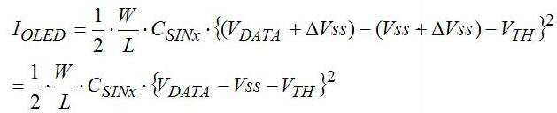
이때, 상기 스토리지 캐패시터(C41)에 충전된 데이터전압(VDATA)이 구동 트랜지스터(TFT43)의 게이트에 공급되어 그 구동 트랜지스터(TFT43)가 턴온되지만, 상기 설명에서와 같이 유기발광다이오드(OLED41)의 애노드측으로의 상위전원전압(VDD)의 공급을 차단하였으므로 유기발광다이오드(OLED41)의 구동전류 IOLED = 0이 된다. At this time, the data voltage V DATA charged in the storage capacitor C41 is supplied to the gate of the driving transistor TFT43 so that the driving transistor TFT43 is turned on. However, as described above, the data voltage V DATA of the organic light emitting diode OLED41 The supply of the higher power supply voltage VDD to the anode side is cut off, so that the driving current I OLED of the organic
하지만, 이때 상기 스위칭 트랜지스터(TFT42)를 통해 상기 구동 트랜지스터(TFT43)의 드레인에 데이터전압(VDATA)이 공급되므로, 이를 통해 다음의 [수학식1]과 같은 구동전류가 흐르게 된다. However, since the data voltage V DATA is supplied to the drain of the driving transistor TFT43 through the switching transistor TFT42, the driving current as shown in the following Equation (1) flows.
![]()
![]()
이후, 이미션주기(P2)에 도달되면, 상기 스위칭 트랜지스터(TFT41)가 턴오프되므로 게이트노드는 전기적으로 플로팅 상태가 된다. 따라서, 이미션주기(P2)에서 도 4의 화소 구동회로(43)는 도 6b의 등가회로와 같이 구성된다. Thereafter, when the emission period P2 is reached, the switching transistor TFT41 is turned off, so that the gate node becomes electrically floating. Therefore, in the emission period P2, the
상기, 이미션주기(P2)에서 상기 유기발광다이오드(OLED41)의 애노드에 상기 상위전원전압(VDD)이 공급된다. The upper power supply voltage VDD is supplied to the anode of the organic light emitting diode OLED41 in the emission period P2.
상기 구동 트랜지스터(TFT43)의 게이트에는 이미 상기 스토리지 캐패시터(C41)에 저장된 데이터전압(VDATA)이 공급되고 있으므로, 이에 의해 그 구동 트랜지스터(TFT43)가 턴온된다. 이에 따라, 상기 유기발광다이오드(OLED41) 및 구동 트랜지스터(TFT43)를 통해 하위전원전압(Vss) 단자 측으로 전류가 흘러 그 유기발광다이오드(OLED41)가 발광된다. Since the data voltage V DATA stored in the storage capacitor C41 is already supplied to the gate of the driving transistor TFT43, the driving transistor TFT43 is turned on. Accordingly, a current flows to the lower power supply voltage (Vss) terminal side through the organic light emitting diode OLED41 and the driving transistor TFT43, and the organic light emitting diode OLED41 emits light.
그런데, 표시패널(40)상의 Vss 배선에는 저항 성분이 존재하므로, 그 Vss 배선을 통해 전류가 흐르는 것에 의해 하위전원전압(Vss)의 전위가 상승되는 현상이 발생된다. 이를 하위전위 상승(Vss rising)이라 한다. However, since the resistance component exists in the Vss wiring on the
하지만, 본 발명의 화소 구동 장치에서는 하위전원전압(Vss)의 전위가 상승될 때 스토리지 캐패시터(C41)에 의해 구동 트랜지스터(TFT43)의 게이트 노드가 커플링되어 이 게이트 노드의 전압도 동일하게 상승된다. 이에 의해 하위전원전압(Vss)의 전위가 상승 문제가 해소된다. 다음의 [수학식2]는 이미션주기(P2)에서 상기 유기발광다이오드(OLED41)의 구동전류를 나타낸 것이다.However, in the pixel driving apparatus of the present invention, when the potential of the lower power supply voltage Vss rises, the gate node of the driving transistor TFT43 is coupled by the storage capacitor C41 so that the voltage of the gate node is also raised . As a result, the problem of rising of the potential of the lower power supply voltage Vss is solved. The following equation (2) represents the driving current of the organic light emitting

도 8a 및 도 8b는 도 5의 전류 기입형 화소 구동회로(53)에서 스위칭 트랜지스터(TFT41),(TFT42)의 스위칭 동작에 따른 온,오프 등가회로를 나타낸 것이다.8A and 8B show on / off equivalent circuits according to the switching operation of the switching transistors TFT41 and TFT42 in the current-writing type
유기발광다이오드(OLED41)의 애노드에 1 프레임 내내 상위전원전압(VDD)을 공급하는 것이 아니라, 1 프레임 중 프로그래밍주기(P1)에서는 그 상위전원전압(VDD)의 공급을 차단한다. 이와 같은 상태에서 정극성의 스캔신호(SCAN1∼SCANn)가 각 수평라인에 순차적으로 공급된다.The power supply voltage VDD is not supplied to the anode of the organic light emitting diode OLED41 within one frame but the supply of the upper power supply voltage VDD is interrupted during the programming period P1 of one frame. In this state, the positive scan signals SCAN1 to SCANn are sequentially supplied to the respective horizontal lines.
상기 프로그래밍주기(P1)에서 해당 스캔신호(SCAN)에 의해 스위칭 트랜지스터(TFT41)가 턴온되므로 해당 데이터라인을 통해 공급되는 데이터전류(IDATA)가 그 스위칭 트랜지스터(TFT41)를 통해 스토리지 캐패시터(C41)에 전달되어 데이터전류(IDATA)를 허용하기 위한 레벨의 전압(VDATA)이 셋팅되고, 이는 이미션주기(P2)까지 유지된다. 이와 동시에, 상기 스위칭 트랜지스터(TFT41)에 공급되는 스캔신호(SCAN)에 의해 스위칭 트랜지스터(TFT42)가 턴온되는데, 이는 후술하는 바와 같이 드레쉬홀드 전압의 보상을 위해 센싱전류를 공급하기 위한 것으로 데이터 전류의 프로그래밍 동작에는 별다른 영향을 미치지 않는다.The switching transistor TFT41 is turned on by the corresponding scan signal SCAN in the programming period P1 so that the data current I DATA supplied through the corresponding data line is supplied to the storage capacitor C41 through the switching transistor TFT41. And a voltage (V DATA ) of a level for allowing the data current (I DATA ) is set, which is maintained until the emission period (P2). At the same time, the switching transistor TFT42 is turned on by the scan signal SCAN supplied to the switching transistor TFT41. This is to supply the sensing current for compensation of the threshold voltage, The programming operation of the memory cell is not affected.
따라서, 프로그래밍주기(P1)에서 도 5의 화소 구동회로(53)는 도 8a의 등가회로와 같이 구성된다. Therefore, in the programming period P1, the
이때, 상기 데이터전류(IDATA)에 의해 상기 스토리지 캐패시터(C41)에 충전된 데이터전압(VDATA)이 구동 트랜지스터(TFT43)의 게이트에 공급되어 그 구동 트랜지스터(TFT43)가 턴온되지만, 상기 설명에서와 같이 유기발광다이오드(OLED41)의 애노드측으로의 상위전원전압(VDD)의 공급을 차단하였으므로 유기발광다이오드(OLED41) 의 구동전류 IOLED = 0이 된다. At this time, the data voltage (V DATA ) charged in the storage capacitor C41 is supplied to the gate of the driving transistor TFT43 by the data current I DATA so that the driving transistor TFT43 is turned on. However, The supply of the upper power source voltage VDD to the anode side of the organic
하지만, 이때 상기 스위칭 트랜지스터(TFT42)를 통해 상기 구동 트랜지스터(TFT43)의 드레인에 데이터전류(IDATA)가 공급되므로, 이를 통해 다음의 [수학식3]과 같은 구동전류가 흐르게 된다. However, since the data current I DATA is supplied to the drain of the driving transistor TFT43 through the switching transistor TFT42, the driving current shown in the following Equation (3) flows.

이후, 이미션주기(P2)에 도달되면, 상기 스위칭 트랜지스터(TFT41)가 턴오프되므로 게이트노드는 전기적으로 플로팅 상태가 된다. 따라서, 이미션주기(P2)에서 도 5의 화소 구동회로(53)는 도 8b의 등가회로와 같이 구성된다. Thereafter, when the emission period P2 is reached, the switching transistor TFT41 is turned off, so that the gate node becomes electrically floating. Therefore, in the emission period P2, the
상기, 이미션주기(P2)에서 상기 유기발광다이오드(OLED41)의 애노드에 상기 상위전원전압(VDD)이 공급된다. The upper power supply voltage VDD is supplied to the anode of the organic light emitting diode OLED41 in the emission period P2.
상기 구동 트랜지스터(TFT43)의 게이트에는 이미 상기 스토리지 캐패시터(C41)에 저장된 데이터전압(VDATA)이 공급되고 있으므로, 이에 의해 그 구동 트랜지스터(TFT43)가 턴온된다. 이에 따라, 상기 유기발광다이오드(OLED41) 및 구동 트랜지스터(TFT43)를 통해 하위전원전압(Vss) 단자 측으로 전류가 흘러 그 유기발광다이오드(OLED41)가 발광된다. Since the data voltage V DATA stored in the storage capacitor C41 is already supplied to the gate of the driving transistor TFT43, the driving transistor TFT43 is turned on. Accordingly, a current flows to the lower power supply voltage (Vss) terminal side through the organic light emitting diode OLED41 and the driving transistor TFT43, and the organic light emitting diode OLED41 emits light.
그런데, 표시패널(40)상의 Vss 배선에는 저항 성분이 존재하므로, 그 Vss 배선을 통해 전류가 흐르는 것에 의해 하위전원전압(Vss)의 전위가 상승되는 현상이 발생된다. 이를 하위전위 상승(Vss rising)이라 한다. However, since the resistance component exists in the Vss wiring on the
하지만, 본 발명의 화소 구동 장치에서는 하위전원전압(Vss)의 전위가 상승될 때 스토리지 캐패시터(C41)에 의해 구동 트랜지스터(TFT43)의 게이트 노드가 커플링되어 이 게이트 노드의 전압도 동일하게 상승된다. 이에 의해 하위전원단자(Vss)의 전위가 상승 문제가 해소된다. 다음의 [수학식4]는 이미션주기(P2)에서 상기 유기발광다이오드(OLED41)의 구동전류를 나타낸 것이다.However, in the pixel driving apparatus of the present invention, when the potential of the lower power supply voltage Vss rises, the gate node of the driving transistor TFT43 is coupled by the storage capacitor C41 so that the voltage of the gate node is also raised . Thereby, the problem of rising of the potential of the lower power supply terminal Vss is solved. The following equation (4) represents the driving current of the organic light emitting
그런데, 상기의 설명에서와 같이 하나의 상위전원전압(VDD)의 단자를 공통으로 사용하여 화소를 구동하는 방식의 경우, 1 프레임 중에서 프로그래밍주기(P1)를 제외한 시간이 이미션주기(P2) 즉, 유기발광다이오드(OLED41)의 점등시간으로 결정되어 그만큼 유기발광다이오드(OLED41)의 점등시간이 줄어드는 문제점이 발생된다. However, as described above, in the case of driving a pixel by commonly using one terminal of the higher power supply voltage VDD, the time except for the programming period P1 in one frame is equal to the emission period P2 , And the lighting time of the organic light emitting diode (OLED) 41 is determined as the lighting time of the organic light emitting diode (OLED) 41.
표시패널(40)이 소형인 경우, 비교적 스캔라인의 수가 적으므로 상기와 같이 하나의 상위전원전압(VDD)의 단자를 공통으로 사용하여 화소를 구동하더라도 상기 프로그래밍주기(P1)에 별다른 영향을 받지 않고 유기발광다이오드(OLED41)의 점등시간을 확보할 수 있다.When the
그러나, 상기 표시패널(40)이 대형(예, 스캔라인수: 768)인 경우에는 비교적 스캔라인의 수가 많으므로 상기와 같은 방식으로 화소를 구동하는 경우, 상기 프로그래밍주기(P1)가 비교적 많이 늘어나 유기발광다이오드(OLED41)의 점등시간을 필요한 만큼 확보하는데 어려움이 있어 휘도 플리커 현상이 발생된다.However, when the
따라서, 표시패널(40)이 소형이거나 대형인 것에 관계없이 프로그래밍주기(P1)와 유기발광다이오드(OLED41)의 점등시간을 충분히 확보할 수 구동방식이 제안되었는데, 도 9를 참조하여 이 구동방식에 대하여 설명한다.Therefore, a driving method has been proposed in which the programming period P1 and the lighting time of the organic light emitting
이와 같은 표시패널(40)은, 이웃하는 복수 개수의 스캔라인들이 포함되도록 수평방향으로 복수개의 표시패널영역을 정의하고, 그 정의된 각각의 표시패널영역 내의 화소들이 상위전원전압(VDD)의 단자로부터 분기되어 공급되는 상위전원전압[VDD.01∼VDD.10] 중에서 해당 전원전압을 공유하도록 하며, 그 정의된 각각의 표시영역별로 한 프레임 주기내에서 프로그래밍주기(P1)와 이미션주기(P2)가 결정되도록 구성된다.The
이와 같은 경우, 표시패널(40) 내에서 스캔라인(S1∼Sn)과 데이터라인(D1∼Dm)의 배선 형태는 통상의 표시패널에서와 동일하다.In this case, the wiring patterns of the scan lines S1 to Sn and the data lines D1 to Dm in the
하지만, 상기 표시패널(40)을 이웃하는 복수 개수의 스캔라인(또는 수평라인)들이 포함되도록 수평방향으로 복수개의 영역으로 정의하고, 이렇게 정의된 표시패널영역별로 상위전원전압(VDD.01∼VDD.10)을 공급하게 된다.However, the
이에 대한 예로써, 스캔라인(S1∼Sn)이 600개인 대형 표시패널(40)을 10개의 표시패널영역으로 정의하는 것을 들 수 있다. 이와 같은 경우 상기 10개의 표시패 널영역 각각은 60개의 스캔라인[(S1∼S60),(S61∼S120)…(S541∼S600)]이 포함되게 정의된다. For example, a
참고로, 본 발명이 적용된 표시패널(40)은 XGA급(1024×768)을 예로 하였으므로, 상기 스캔라인(S1∼Sn)의 수가 768개 이어야 하나, 설명의 편의상 600개인 것으로 하였다.Since the
또한, 수평방향으로 복수개의 영역으로 정의된 표시패널영역 내에서도 상기 상위전원전압(VDD.01∼VDD.10)의 단자가 다시 분기되어 각각의 해당 전원전압 단자에 연결된다. 예를 들어, 첫번째 표시패널영역에서는 상위전원전압(VDD.01)의 단자가 상기와 같은 방식으로 60개의 전원단자로 분기되어 해당 전원전압의 단자에 공급된다. Also, the terminals of the higher power supply voltages (VDD.01 to VDD.10) are further branched and connected to respective corresponding power supply voltage terminals even in the display panel region defined by a plurality of regions in the horizontal direction. For example, in the first display panel region, the terminal of the higher power supply voltage VDD.01 is branched to 60 power terminals in the same manner as described above and supplied to the terminal of the power supply voltage.
도 9의 (a)-(e)는 상기와 같이 정의되어 각각의 상위전원전압(VDD.01∼VDD.10)이 공급되는 각 표시패널영역에서의 프로그래밍주기(P1) 및 이미션주기(P2), 스캔신호(SCAN.001∼SCAN.600) 및 데이터전압(VDATA)의 타이밍도를 나타낸 것이다. 9A to 9E are diagrams illustrating a programming period P1 and an emission period P2 in each display panel region to which the upper power supply voltages VDD.01 to VDD.10 are supplied, ), The scan signals SCAN.001 to SCAN.600, and the data voltage (V DATA ).
다시 말해서, 상기 도 9의 (a),(b)는 각 표시패널영역에 대한 프로그래밍주기(P1) 및 이미션주기(P2)의 설정예를 나타낸 것이다. 즉, 표시패널(40)에 대하여 10개의 표시패널영역으로 정의된 경우 1 프레임을 10등분하여 1/10 프레임의 주기를 각 표시패널영역의 프로그래밍주기(P1)로 설정하고, 나머지 9/10의 주기를 이미션주기(P2)로 설정한다.In other words, FIGS. 9A and 9B show setting examples of the programming period P1 and the emission period P2 for each display panel region. That is, when 10 display panel areas are defined for the
도 9의 (c),(d)는 각 표시패널영역에 대한 스캔신호(SCAN.001∼SCAN.600)의 타이밍도를 나타낸 것으로, 통상의 스캔 타이밍도와 동일한 것을 알 수 있다. FIGS. 9C and 9D show the timing charts of the scan signals SCAN.001 to SCAN.600 for each display panel region, which is the same as the normal scan timing.
그리고, 도 9의 (e)는 각 표시패널영역을 대상으로 데이터라인(D1∼Dn)을 통해 공급되는 데이터 전압(VDATA)의 타이밍도를 나타낸 것으로, 이 또한 통상의 스캔 타이밍도와 동일한 것을 알 수 있다. 9 (e) shows the timing chart of the data voltage (V DATA ) supplied through the data lines D1 to Dn with respect to each display panel area, .
이와 같은 경우, 예를 들어 첫 번째 표시패널영역의 상위전원전압(VDD.01)이 차단될 때 스캔신호(SCAN.001∼SCAN.60)가 공급되어 그 첫 번째 표시패널영역의 데이터전압을 프로그래밍한다. 이후 상위전원전압(VDD.01)이 공급되는 시점에서 첫 번째 표시패널영역에 대한 이미션이 동시에 이루어진다. 다음의 표시패널영역에 대해서도 동일한 방식으로 프로그래밍과 이미션 동작이 이루어진다.In this case, for example, when the upper power supply voltage VDD.01 of the first display panel region is cut off, the scan signals SCAN.001 to SCAN.60 are supplied to program the data voltage of the first display panel region do. At the time when the upper power supply voltage VDD.01 is supplied, the first display panel region is simultaneously emitted. Programming and emulation operations are performed in the same manner for the following display panel areas.
이렇게 함으로써, 각 상위전원전압(VDD.01∼VDD.10)의 단자가 담당하는 전류량이 대폭적으로 감소되며, 이미션하는 시간도 충분히 확보할 수 있게 된다.By doing so, the amount of current charged by the terminals of the respective higher power supply voltages VDD.01 to VDD.10 is greatly reduced, and the time for the emission can be sufficiently secured.
상기의 설명에서 1 프레임 중 프로그래밍주기(P1) 동안 상기 유기발광다이오드(OLED41) 및 구동 트랜지스터(TFT43)를 통해 전류가 흐르지 않도록 상기 상위전원전압(VDD)의 공급을 차단하는 방법에는 여러 가지가 있을 수 있는데, 도 10은 스위칭 트랜지스터를 이용하여 구현한 예를 나타낸 것이다.In the above description, there are various methods of interrupting the supply of the upper power supply voltage VDD so that current does not flow through the organic light emitting diode OLED41 and the driving transistor TFT43 during the programming period P1 of one frame FIG. 10 shows an example implemented using a switching transistor.
즉, 상기 유기발광다이오드(OLED41)의 캐소우드와 구동 트랜지스터(TFT43)의 드레인 사이에 스위칭 트랜지스터(TFT44)의 드레인과 소스를 각기 접속한다. 그리고, 상기 프로그래밍주기(P1)에서 디스플레이 콘트롤러(41)로 하여금 상기 스위칭 트랜지스터(TFT44)의 게이트에 스위칭 제어신호(EMS)를 '로우'로 출력하도록 하여 그 스위칭 트랜지스터(TFT44)가 턴오프되도록 하는 방식이다.That is, the drain and source of the switching transistor TFT44 are connected between the cathode of the organic light emitting diode OLED41 and the drain of the driving transistor TFT43, respectively. In the programming period P1, the
이상에서는 본 발명에 적용되는 전압 기입형 화소 구동회로(43) 및 전류 기입형 화소 구동회로(53)에서의 Vss 전위가 상승되는 문제를 해결하는 구동방식에 대하여 설명한 것이다. The driving method for solving the problem of increasing the Vss potential in the voltage-writing type
이하, 화소 구동회로에서의 전압 기입형 화소 구동회로(43) 및 전류 기입형 화소 구동회로(53)에서 구동 트랜지스터의 드레쉬홀드전압(Vth)의 변동(Shift)을 검출하여 그에 상응되게 데이터 전압을 보상처리하는 과정에 대하여 상세히 설명한다.Hereinafter, the voltage-writing type
먼저, 도 4의 전압 기입형 화소 구동회로(43)에서의 구동 트랜지스터(TFT43)의 드레쉬홀드전압(Vth)의 변동을 검출하여 그에 상응되게 데이터 전압(VDATA)을 보상처리하는 과정에 대하여 설명한다. First, regarding the process of detecting the variation of the threshold voltage (Vth) of the driving transistor (TFT 43) in the voltage-writing type
디스플레이 콘트롤러(41)의 변조기(41A)는 화소 구동회로(43)상의 타겟 유기발광다이오드(OLED41)가 발광되지 않는 임의의 시점(검출모드)에서 기 설정된 화상신호(DATA)를 데이터 구동부(42)에 출력한다.The
이에 대하여, 상기 데이터 구동부(42)에서는 상기 변조기(41A)로부터 입력되는 화상신호(DATA)의 전압을 연산증폭기(OP1)를 통해 증폭한 후 저항(R1)을 통해 해당 화소 구동회로(43)에 출력한다.The
이때, 스캔신호(SCAN)에 의해 스위칭 트랜지스터(TFT41),(TFT42)가 모두 턴 온된다. 이에 따라, 상기 데이터 구동부(42)에서 출력되는 데이터전압(VDATA)이 상기 스위칭 트랜지스터(TFT41)를 통해 스토리지 캐패시터(C41)에 충전된다.At this time, all the switching transistors TFT41 and TFT42 are turned on by the scan signal SCAN. Accordingly, the data voltage V DATA output from the
상기 스토리지 캐패시터(C41)에 충전된 데이터전압에 의해 상기 구동 트랜지스터(TFT43)가 턴온되므로, 상기 데이터 구동부(42)에서 출력되는 데이터전압(VDATA)에 의해 그 구동 트랜지스터(TFT43)를 통해 해당 전류(ITFT43)가 흐르게 된다. The driving transistor TFT43 is turned on by the data voltage charged in the storage capacitor C41 so that the data voltage V DATA output from the
이때, 상기 연산증폭기(OP1)의 출력단 전압(Vdet)이 A/D변환기(41B)에서 디지털신호로 변환된다. 상기 연산증폭기(OP1)의 출력단 전압(Vdet)은 상기 전류(ITFT43) 값과 저항(R1)의 값을 곱한 값이 된다. 즉, Vdet = ITFT43 × R1이 된다.At this time, the output terminal voltage V det of the operational amplifier OP1 is converted into a digital signal by the A /
연산기(41C)는 상기 디지털신호로 변환된 전압값을 기 저장된 기준값과 비교하여 그 비교 결과를 근거로 상기 구동 트랜지스터(TFT43)의 열화 정도 즉, 드레쉬홀드전압(Vth)의 변동(Shift) 정도를 연산한다. 그리고, 상기 연산기(41C)는 연산된 변동 정도에 상응되는 보상값을 룩업테이블(41D)에 저장한다.The
이후, 상기 변조기(41A)는 외부로부터 입력되는 원시화상신호(Video data)에 상응되는 화상신호(DATA)를 출력하는 이미션모드에서, 상기 룩업테이블(41D)에 저장된 보상값으로 보상하여 출력하게 된다.Thereafter, the
이에 따라, 데이터 구동부(42)에서 출력되는 데이터전압(VDATA)이 상기 구동 트랜지스터(TFT43)의 드레쉬홀드전압(Vth)의 변동(Shift) 정도에 상응되게 보상된 값으로 출력된다.Accordingly, the data voltage V DATA output from the
따라서, 상기 구동 트랜지스터(TFT43)의 드레쉬홀드전압(Vth)의 변동(Shift)이 발생되더라도, 상기와 같은 보상 처리에 의해 유기발광다이오드(OLED41)가 정상적으로 발광된다.Therefore, even if a shift of the threshold voltage Vth of the driving transistor TFT43 occurs, the organic light emitting diode OLED41 is normally emitted by the compensation process as described above.
한편, 도 5의 전류 기입형 화소 구동회로(53)에서의 구동 트랜지스터(TFT43)의 드레쉬홀드전압(Vth)의 변동을 검출하여 그에 상응되게 데이터 전류(IDATA)을 보상처리하는 과정에 대하여 설명한다. On the other hand, regarding the process of detecting the variation of the threshold voltage (Vth) of the driving transistor (TFT 43) in the current writing type
디스플레이 콘트롤러(51)의 변조기(51A)는 화소 구동회로(53)상의 타겟 유기발광다이오드(OLED41)가 발광되지 않는 임의의 시점(검출모드)에서 기 설정된 화상신호(DATA)를 데이터 구동부(52)에 출력한다.The
이에 대하여, 상기 데이터 구동부(52)에서는 상기 변조기(51A)로부터 입력되는 화상신호(DATA)에 상응되는 전류(IDATA)를 해당 화소 구동회로(53)에 출력한다.On the other hand, the
이때, 스캔신호(SCAN)에 의해 스위칭 트랜지스터(TFT41),(TFT42)가 모두 턴온된다. 이에 따라, 상기 데이터 구동부(52)에서 출력되는 데이터전류(IDATA)가 상기 스위칭 트랜지스터(TFT41)를 통해 스토리지 캐패시터(C41)에 공급된다. 이에 따라, 상기 스토리지 캐패시터(C41)에 해당 전압이 충전(셋팅)된다. At this time, all the switching transistors TFT41 and TFT42 are turned on by the scan signal SCAN. Accordingly, the data current I DATA output from the
상기 스토리지 캐패시터(C41)에 셋팅된 전압에 의해 상기 구동 트랜지스터(TFT43)가 턴온되고, 이때 상기 데이터 구동부(52)에서 출력되는 데이터전류(IDATA)가 스위칭 트랜지스터(TFT42)를 통해 그 구동 트랜지스터(TFT43)의 드레인 에 전달되므로 이를 통해 해당 전류(ITFT43)가 흐르게 된다. The driving transistor TFT43 is turned on by the voltage set in the storage capacitor C41 and the data current I DATA output from the
이때, 상기 데이터 구동부(52)의 출력단에는 상기 스토리지 캐패시터(C41)에 셋팅된 전압이 검출전압(Vdet)으로 나타나고, 이는 A/D변환기(51B)에서 디지털신호로 변환된다.At this time, the voltage set in the storage capacitor C41 appears at the output terminal of the
연산기(51C)는 상기 디지털신호로 변환된 전압값을 기 저장된 기준값과 비교하여 그 비교 결과를 근거로 상기 구동 트랜지스터(TFT43)의 열화 정도 즉, 드레쉬홀드전압(Vth)의 변동(Shift) 정도를 연산한다. 그리고, 상기 연산기(51C)는 연산된 변동 정도에 상응되는 보상값을 룩업테이블(51D)에 저장한다.The
이후, 상기 변조기(51A)는 외부로부터 입력되는 원시화상신호(Video data)에 상응되는 화상신호(DATA)를 출력하는 이미션모드에서, 상기 룩업테이블(51D)에 저장된 보상값으로 보상하여 출력하게 된다.Thereafter, the
이에 따라, 데이터 구동부(52)에서 출력되는 데이터전류(IDATA)가 상기 구동 트랜지스터(TFT43)의 드레쉬홀드전압(Vth)의 변동(Shift) 정도에 상응되게 보상된 값으로 출력된다.Accordingly, the data current I DATA output from the
따라서, 상기 구동 트랜지스터(TFT43)의 드레쉬홀드전압(Vth)의 변동(Shift)이 발생되더라도, 상기와 같은 보상 처리에 의해 유기발광다이오드(OLED41)가 정상적으로 발광된다.Therefore, even if a shift of the threshold voltage Vth of the driving transistor TFT43 occurs, the organic light emitting diode OLED41 is normally emitted by the compensation process as described above.
한편, 본 발명의 다른 실시예에서는 별도의 전류 센싱라인을 구비하고 BDI(BDI: Black Data Insertion)와 같은 특정 구간(시간)을 이용하여 화소구동회로 상의 구동 트랜지스터의 전류를 센싱하고, 이를 근거로 상기 설명에서와 같이 구동트랜지스터의 드레쉬홀드전압(Vth)의 변동(Shift) 정도를 분석하여 보상하도록 하였는데, 이하 이에 대하여 설명한다.In another embodiment of the present invention, a current sensing line is provided and the current of the driving transistor on the pixel driving circuit is sensed using a specific period (time) such as BDI (BDI: Black Data Insertion) The shift amount of the threshold voltage Vth of the driving transistor is analyzed and compensated for as described above.
도 11은 본 발명의 다른 실시예에 따른 기본 화소구동회로도로서, 이에 도시한 바와 같이 프로그래밍 주기나 구동트랜지스터의 드레쉬홀드전압의 변동 정도를 검출하는 검출모드에서 스캔신호(SCAN1)에 의해 턴온되어 데이터라인을 통해 공급되는 데이터전압(VDATA)을 스토리지 캐패시터(C22)에 전달하는 스위칭 트랜지스터(TFT22A)와; 검출모드에서 스캔신호(SCAN2)에 의해 턴온되어 별도로 구비된 센싱라인을 통해 공급되는 센싱전압을 구동 트랜지스터(TFT22C)의 드레인에 전달하는 스위칭 트랜지스터(TFT22B)와; 구동 트랜지스터(TFT22C)의 게이트단자와 하위전원전압(Vss) 단자 사이에 접속되어 상기 데이터전압(VDATA)을 차징하는 스토리지 캐패시터(C22)와; 이미션모드에서 상기 스토리지 캐패시터(C22)에 차징된 데이터전압(VDATA)에 상응되는 구동전류가 유기발광다이오드(OLED22)에 공급되도록 하고, 검출모드에서는 게이트에 공급되는 상기 차징된 데이터전압(VDATA)과 상기 스위칭 트랜지스터(TFT22B)를 통해 드레인에 공급되는 센싱전압에 의해 구동되는 구동 트랜지스터(TFT22C)와; 애노드가 상위전원전압(VDD) 단자에 접속되고 캐소우드가 상기 구동 트랜지스터(TFT2C)의 드레인에 접속되어, 상기 구동전류에 상응되는 밝기로 발광하는 유기발광다이오드(OLED22)로 구성한 것으로, 이와 같이 구성한 본 발명의 다른 실시예의 작용을 도 12 내지 도 14를 참조하여 상세히 설명하면 다음과 같다.11 is a basic pixel driving circuit diagram according to another embodiment of the present invention. As shown in FIG. 11, when the scan signal SCAN1 is turned on in a detection mode for detecting a programming period or a fluctuation degree of a threshold voltage of a driving transistor A switching transistor (TFT22A) for transferring a data voltage (V DATA ) supplied through the data line to the storage capacitor (C22); A switching transistor TFT22B which is turned on by the scan signal SCAN2 in the detection mode and transfers a sensing voltage supplied through a separately provided sensing line to the drain of the driving transistor TFT22C; A storage capacitor C22 connected between the gate terminal of the driving transistor TFT22C and the lower power supply voltage Vss to charge the data voltage V DATA ; The driving current corresponding to the data voltage V DATA charged in the storage capacitor C22 is supplied to the organic light emitting diode OLED22 in the emission mode and the charged data voltage V And a driving transistor (TFT22C) driven by a sensing voltage supplied to the drain through the switching transistor (TFT22B); And an organic light emitting diode (OLED) 22 in which an anode is connected to a higher power supply voltage (VDD) terminal and a cathode is connected to a drain of the driving transistor (TFT2C) and emits light with brightness corresponding to the driving current. The operation of another embodiment of the present invention will be described in detail with reference to FIG. 12 to FIG.
본 발명의 다른 실시예에서의 기본적인 화소구동회로는 도 11과 같이 구성되고, 이와 같은 화소 구동회로가 표시패널상에 매트릭스 형태로 배열되는데, 그 표시패널의 일부를 나타낸 것이 도 12이다. 그리고, 도 13a은 상기 도 11에서의 프로그래밍주기의 타이밍도를 나타낸 것이고, 도 13b는 검출모드에서의 전류 센싱에 대한 타이밍도를 나타낸 것이다.A basic pixel driver circuit in another embodiment of the present invention is configured as shown in FIG. 11, and such pixel driver circuits are arranged in a matrix form on a display panel. FIG. 12 shows a part of the display panel. FIG. 13A is a timing chart of the programming cycle in FIG. 11, and FIG. 13B is a timing chart for current sensing in the detection mode.
각 화소구동회로 예를 들어, 화소구동회로(PX22)에서 두 개의 트랜지스터(TFT22A),(TFT22C)와 한 개의 스토리지 캐패시터(C22)를 이용한 프로그래밍 동작은 통상의 화소 구동회로에서와 같이 동작한다. For example, the programming operation using two transistors (TFT22A, TFT22C) and one storage capacitor C22 in the pixel driver circuit (PX22) operates as in a normal pixel driver circuit.
즉, 프로그래밍주기(또는 데이터 어드레스 주기)에서 도 13a와 같이 스캔신호(SCAN1)와 데이터전압(VDATA)이 '하이'로 공급된다. 이에 따라, 스위칭 트랜지스터(TFT22A)가 턴온되어 데이터라인을 통해 공급되는 상기 데이터전압(VDATA)이 스토리지 캐패시터(C22)에 충전되어 이미션(Emission)주기까지 유지된다.That is, the scan signal SCAN1 and the data voltage V DATA are supplied at a high level in the programming period (or the data address period) as shown in FIG. 13A. Accordingly, the data voltage V DATA supplied through the data line is turned on by the switching transistor TFT 22A is charged in the storage capacitor C22 and maintained until the emission period.
이후, 이미션 주기에서, 상기 스토리지 캐패시터(C22)에 충전된 데이터전압(VDATA)에 의해 구동 트랜지스터(TFT22C)가 턴온되어 그 데이터전압(VDATA)에 상응되는 양의 전류가 유기발광다이오드(OLED22)를 통해 흐르게 되므로 그 유기발광다이오드(OLED22)가 해당 전류량의 밝기로 발광하게 된다.Then, in the emission cycle, the storage capacitor (C22) of the data voltage (V DATA) drive transistor (TFT22C) is turned on a current organic light emitting diode of the amount corresponding to the data voltage (V DATA) by charging the ( OLED 22, so that the organic light emitting diode OLED 22 emits light with a brightness corresponding to the amount of current.
한편, 검출모드에서 BDI(BDI: Black Data Insertion)와 같은 특정 구간(시간)을 이용하여 소정 주기로 화소구동회로를 선택하여 해당 구동 트랜지스터의 전류를 검출하게 되는데, 본 설명에서는 화소구동회로(PX22)를 선택하여 전류를 검출 하는 것을 예로 하여 설명한다.On the other hand, in the detection mode, the pixel driving circuit is selected at a predetermined cycle by using a specific period (time) such as BDI (BDI: Black Data Insertion) To detect the current is described as an example.
먼저, 제1스텝에서 1 프레임 중 BDI 구간에 맞춰 스캔라인의 스캔신호(SCAN1.n+1)를 '하이'로 출력하고 다른 스캔라인의 스캔신호(SCAN1.n)를 '로우'로 출력한다. 이에 따라, 화소구동회로(PX21),(PX22)의 스위칭 트랜지스터(TFT21A),(TFT22A)가 턴온되고, 다른 화소구동회로(PX11),(PX12)의 해당 스위칭 트랜지스터(TFT11A),(TFT12A)는 턴오프된다.First, in a first step, the scan signal SCAN1.n + 1 of the scan line is output as 'HIGH' and the scan signal SCAN1.n of the other scan line is output as 'LOW' in accordance with the BDI interval of one frame . Thus, the switching transistors TFT21A and TFT22A of the pixel driver circuits PX21 and PX22 are turned on and the corresponding switching transistors TFT11A and TFT12A of the other pixel driver circuits PX11 and PX12 are turned on Off.
이때, 데이터라인의 데이터전압(VDATA.m+1)을 5V로 공급하고, 다른 데이터라인의 데이터전압(VDATA.m)을 0V(또는 부극성 전압)로 공급한다. 이에 따라, 화소구동회로(PX22)의 스토리지 캐패시터(C22)에 상기 5V 전압이 충전되고 나머지 화소구동회로(PX11),(PX12),(PX21)의 스토리지 캐패시터(C11),(C12),(C21)에는 전압이 충전되지 않는다. At this time, the data voltage (V DATA.m + 1 ) of the data line is supplied at 5 V and the data voltage (V DATA.m ) of the other data line is supplied at 0 V (or a negative voltage). Thus, the storage capacitor C22 of the pixel drive circuit PX22 is charged with the 5V voltage and the storage capacitors C11, C12, and C21 of the remaining pixel drive circuits PX11, PX12, The voltage is not charged.
이후, 제2스텝에서 상기 스캔라인의 스캔신호(SCAN1.n+1)를 '로우'로 출력하여 상기 화소구동회로(PX21),(PX22)의 스위칭 트랜지스터(TFT21A),(TFT22A)가 턴오프된다. 이와 동시에 스캔라인의 스캔신호(SCAN2.n+1)를 '하이'로 출력하여 스위칭 트랜지스터(TFT21B),(TFT22B)가 턴온된다.Then, in a second step, the scan signal SCAN1.n + 1 of the scan line is outputted as 'LOW', and the switching transistors TFT21A and TFT22A of the pixel driving circuits PX21 and PX22 are turned off do. At the same time, the scan signal SCAN2.n + 1 of the scan line is outputted as high, and the switching transistors TFT21B and TFT22B are turned on.
이와 같은 상태에서 센싱라인의 센싱신호(SENSE)를 15V로 공급한다. 이에 따라, 상기 센싱라인을 통해 공급되는 15V의 센싱신호(SENSE)가 상기 화소구동회로(PX22)의 스위칭 트랜지스터(TFT22B)를 통해 구동트랜지스터(TFT22C)의 드레인에 전달되지만, 나머지 화소구동회로(PX11),(PX12),(PX21)에는 아무런 영향을 주지 못 한다. In this state, the sensing signal SENSE of the sensing line is supplied at 15V. Accordingly, the sensing signal SENSE of 15 V supplied through the sensing line is transferred to the drain of the driving transistor TFT22C through the switching transistor TFT22B of the pixel driving circuit PX22, but the remaining pixel driving circuits PX11 ), (PX12), and (PX21).
왜냐하면, 화소구동회로(PX11),(PX12)에서는 스위칭 트랜지스터(TFT11B),(TFT12B)가 오프되어 있으므로 상기 센싱라인(SENSE)을 통해 공급되는 15V 전압이 구동트랜지스터(TFT11C),(TFT12C)의 드레인에 전달되지 않고, 화소구동회로(PX21)에서는 스위칭 트랜지스터(TFT21B)가 턴온 상태이지만 구동 트랜지스터(TFT21C)의 게이트 전압이 OV이므로 그 구동 트랜지스터(TFT21C)가 턴오프 상태로 유지되고 있기 때문이다.This is because the switching transistors TFT11B and TFT12B are turned off in the pixel driving circuits PX11 and PX12 so that the 15V voltage supplied through the sensing line SENSE flows to the drain of the driving transistors TFT11C and TFT12C This is because the switching transistor TFT 21B is turned on in the pixel driving circuit PX21 but the gate voltage of the driving transistor TFT 21C is OV so that the driving transistor TFT 21C is kept in the turned off state.
이때, 상기 화소구동회로(PX22)의 유기발광다이오드(OLED22)는 역전압 또는 상위전원전압(VDD)의 차단으로 인하여 오프(소등) 상태로 된다. At this time, the organic light emitting diode OLED22 of the pixel driving circuit PX22 is turned off (turned off) due to the reverse voltage or the interruption of the upper power supply voltage VDD.
결국, 상기와 같은 과정을 통해 화소구동회로(PX22)의 구동 트랜지스터(TFT22C)를 검출모드로 구동하고, 이에 대하여 상기 센싱라인을 통해 도 4 또는 도 5에서와 같이 드레쉬홀드전압(Vth)의 변동(Shift)을 검출하여 변동분 만큼 보상처리하게 된다.As a result, the driving transistor TFT22C of the pixel driving circuit PX22 is driven in the detection mode through the above process, and the driving transistor TFT22C of the pixel driving circuit PX22 is driven through the sensing line, Shift is detected and compensated for by the amount of variation.
도 14는 본 발명의 다른 실시예에서 구동트랜지스터의 드레쉬홀드전압(Vth)의 변동(Shift) 정도를 분석하는 구간의 예로써, BDI 구간을 나타낸 것이다. 여기서 X 축의 구간은 프레임 시간에 해당되는 구간이며, Y 축은 표시패널에서 스캔신호(SCAN)가 공급되는 구간에 해당된다. 상기 BDI 구간은 1 프레임의 10% 정도로서 이 구간에서는 유기 발광다이오드의 이미션 동작이 이루어지지 않는다. 따라서, BDI 구동 방식에 따라 상기 드레쉬홀드전압의 변동 검출회수가 결정된다. 예를 들어 9:1 BDI인 경우 1 프레임 당 드레쉬홀드전압의 변동 검출이 가능한 화소수는 최 대 10개가 된다. 따라서, 각 프레임의 BDI마다 소정 주기로 각 화소를 순차적으로 선택하면서 그 때마다 해당 구동트랜지스터의 드레쉬홀드전압(Vth)의 변동(Shift) 정도를 분석하게 된다.FIG. 14 shows a BDI section as an example of a section for analyzing the degree of shift of the threshold voltage (Vth) of the driving transistor in another embodiment of the present invention. Here, the X axis corresponds to the frame time, and the Y axis corresponds to the scan signal SCAN supplied to the display panel. The BDI interval is about 10% of one frame, and the emission operation of the organic light emitting diode is not performed in this interval. Therefore, the number of fluctuation detection of the threshold voltage is determined according to the BDI driving method. For example, in the case of 9: 1 BDI, the maximum number of pixels that can detect variation of the threshold voltage per frame is 10. Accordingly, each pixel is sequentially selected at predetermined intervals for each BDI of each frame, and the degree of shift of the threshold voltage (Vth) of the corresponding driving transistor is analyzed each time.
도 1은 종래 기술에 의한 유기전계 발광표시장치의 블록도.1 is a block diagram of an organic light emitting display according to a related art.
도 2는 도 1에서 유기전계발광 표시패널상에 배열된 화소의 구동회로도.FIG. 2 is a driving circuit diagram of a pixel arranged on an organic light emitting display panel in FIG. 1; FIG.
도 3은 도 2에서 스캔신호 및 데이터전압의 파형도.FIG. 3 is a waveform diagram of a scan signal and a data voltage in FIG. 2; FIG.
도 4는 본 발명에 의한 유기전계발광 표시장치의 화소 구동 장치의 블록도.4 is a block diagram of a pixel driving apparatus of an organic light emitting display device according to the present invention.
도 5는 본 발명에 의한 유기전계발광 표시장치의 화소 구동 장치의 다른예시 블록도.5 is another exemplary block diagram of a pixel driving apparatus of an organic light emitting display device according to the present invention.
도 6a 및 6b는 도 4의 전압 기입형 화소 구동회로에서 트랜지스터의 스위칭 동작에 따른 온,오프 등가회로도.6A and 6B are circuit diagrams of an on-off equivalent circuit according to a switching operation of a transistor in the voltage-write type pixel driver circuit of FIG.
도 7은 화소구회로의 구동 타이밍도.7 is a driving timing chart of the pixel sphere circuit.
도 8a 및 도 8b는 도 5의 전류 기입형 화소 구동회로에서 트랜지스터의 스위칭 동작에 따른 온,오프 등가회로도.Fig. 8A and Fig. 8B are circuit diagrams of an on-off equivalent circuit according to a switching operation of a transistor in the current-writing type pixel driving circuit of Fig.
도 9의 (a)-(e)는 본 발명에 따른 표시패널의 구동 타이밍도.9 (a) - (e) are driving timing diagrams of a display panel according to the present invention.
도 10은 상위전원전압의 공급을 차단하기 위해 스위칭 트랜지스터를 포함한 화소구동회로도.10 is a pixel driving circuit diagram including a switching transistor for interrupting the supply of an upper power supply voltage.
도 11은 본 발명의 다른 실시예에 따른 기본 화소구동회로도.11 is a basic pixel driving circuit diagram according to another embodiment of the present invention.
도 12는 본 발명의 다른 실시예가 적용된 표시패널의 부분 회로도.12 is a partial circuit diagram of a display panel to which another embodiment of the present invention is applied;
도 13a은 도 11에서의 프로그래밍주기의 타이밍도.13A is a timing diagram of the programming cycle in FIG.
도 13b는 검출모드에서의 전류 센싱에 대한 타이밍도.13B is a timing diagram for current sensing in the detection mode.
도 14는 본 발명이 적용되는 BDI 구간을 나타낸 화면의 개념도.14 is a conceptual diagram of a screen showing a BDI section to which the present invention is applied.
***도면의 주요 부분에 대한 부호의 설명*** DESCRIPTION OF THE REFERENCE SYMBOLS
41 : 디스플레이 콘트롤러 41A : 변조기41:
41B : A/D변환기 41C : 연산기41B: A /
41D : 룩업테이블 42 : 데이터 구동부41D: Lookup table 42: Data driver
43 : 화소구동회로43:
Claims (11)
Priority Applications (3)
| Application Number | Priority Date | Filing Date | Title |
|---|---|---|---|
| KR1020070112916A KR101416904B1 (en) | 2007-11-07 | 2007-11-07 | Driving apparatus for organic electro-luminescence display device |
| US12/289,912 US10089934B2 (en) | 2007-11-07 | 2008-11-06 | Driving apparatus for organic electro-luminescence display device |
| CN2008101755713A CN101430862B (en) | 2007-11-07 | 2008-11-07 | Driving apparatus for organic electro-luminescence display device |
Applications Claiming Priority (1)
| Application Number | Priority Date | Filing Date | Title |
|---|---|---|---|
| KR1020070112916A KR101416904B1 (en) | 2007-11-07 | 2007-11-07 | Driving apparatus for organic electro-luminescence display device |
Publications (2)
| Publication Number | Publication Date |
|---|---|
| KR20090046983A KR20090046983A (en) | 2009-05-12 |
| KR101416904B1 true KR101416904B1 (en) | 2014-07-09 |
Family
ID=40646227
Family Applications (1)
| Application Number | Title | Priority Date | Filing Date |
|---|---|---|---|
| KR1020070112916A KR101416904B1 (en) | 2007-11-07 | 2007-11-07 | Driving apparatus for organic electro-luminescence display device |
Country Status (3)
| Country | Link |
|---|---|
| US (1) | US10089934B2 (en) |
| KR (1) | KR101416904B1 (en) |
| CN (1) | CN101430862B (en) |
Families Citing this family (62)
| Publication number | Priority date | Publication date | Assignee | Title |
|---|---|---|---|---|
| KR101518324B1 (en) * | 2008-09-24 | 2015-05-11 | 삼성디스플레이 주식회사 | Display device and driving method thereof |
| CN102044213B (en) * | 2009-10-21 | 2013-12-18 | 京东方科技集团股份有限公司 | Current-driven pixel circuit, drive method thereof and organic light emitting display device |
| KR101388286B1 (en) * | 2009-11-24 | 2014-04-22 | 엘지디스플레이 주식회사 | Organic Light Emitting Diode Display And Driving Method Thereof |
| KR101223488B1 (en) * | 2010-05-11 | 2013-01-17 | 삼성디스플레이 주식회사 | Organic Light Emitting Display and Driving Method Thereof |
| KR101751998B1 (en) * | 2010-07-22 | 2017-06-28 | 엘지디스플레이 주식회사 | Organic Light Emitting Diode Display And Driving Method Thereof |
| KR101101554B1 (en) * | 2010-08-19 | 2012-01-02 | 한국과학기술원 | Active organic light-emitting display |
| KR101536129B1 (en) | 2011-10-04 | 2015-07-14 | 엘지디스플레이 주식회사 | Organic light-emitting display device |
| KR101463651B1 (en) * | 2011-10-12 | 2014-11-20 | 엘지디스플레이 주식회사 | Organic light-emitting display device |
| TWI467546B (en) * | 2012-03-13 | 2015-01-01 | Chunghwa Picture Tubes Ltd | Driving circuit of an organic light-emitting diode |
| CN102655703B (en) * | 2012-03-23 | 2014-09-24 | 华映视讯(吴江)有限公司 | Driving circuit of organic light-emitting diode |
| US8946994B2 (en) * | 2012-09-25 | 2015-02-03 | Lg Display Co., Ltd. | Organic light emitting display device and driving method thereof |
| CN102881257B (en) * | 2012-10-18 | 2015-02-04 | 四川虹视显示技术有限公司 | Active organic light-emitting diode displayer and driving method thereof |
| KR101992904B1 (en) * | 2012-12-21 | 2019-06-26 | 엘지디스플레이 주식회사 | Organic light emitting diode display device and driving method the same |
| KR102007370B1 (en) * | 2012-12-24 | 2019-08-06 | 엘지디스플레이 주식회사 | Organic light emitting display device and method for driving the same |
| CN103268756B (en) * | 2013-05-29 | 2015-03-18 | 中国科学院上海高等研究院 | AMOLED voltage external compensation method and system |
| CN103413533B (en) * | 2013-07-26 | 2015-07-15 | 北京京东方光电科技有限公司 | Control circuit and display device |
| CN103400547B (en) * | 2013-07-30 | 2015-07-01 | 上海交通大学 | AMOLED direct electric signal mixing feedback circuit and driving method thereof |
| KR102074719B1 (en) * | 2013-10-08 | 2020-02-07 | 엘지디스플레이 주식회사 | Organic light emitting display device |
| KR102084711B1 (en) * | 2013-10-10 | 2020-04-16 | 삼성디스플레이 주식회사 | Display deviceand driving method thereof |
| KR102223552B1 (en) | 2013-12-04 | 2021-03-04 | 엘지디스플레이 주식회사 | Organic light emitting display device and method for driving thereof |
| KR102117889B1 (en) * | 2013-12-11 | 2020-06-02 | 엘지디스플레이 주식회사 | Pixel circuit of display device, organic light emitting display device and method for driving thereof |
| KR102173218B1 (en) | 2013-12-13 | 2020-11-03 | 엘지디스플레이 주식회사 | Organic light emitting display device |
| US10839734B2 (en) | 2013-12-23 | 2020-11-17 | Universal Display Corporation | OLED color tuning by driving mode variation |
| CN104732921B (en) * | 2013-12-23 | 2019-03-01 | 环球展览公司 | The color tuning and its purposes that OLED is changed by drive mode |
| KR102102251B1 (en) * | 2013-12-24 | 2020-04-20 | 엘지디스플레이 주식회사 | Organic light emitting display device |
| KR102192475B1 (en) | 2013-12-24 | 2020-12-17 | 엘지디스플레이 주식회사 | Display device |
| KR102083458B1 (en) * | 2013-12-26 | 2020-03-02 | 엘지디스플레이 주식회사 | Organic Light Emitting Display and Image Quality Compensation Method Of The Same |
| KR102103241B1 (en) | 2013-12-26 | 2020-04-22 | 엘지디스플레이 주식회사 | Organic light emitting diode display device and method of sensing driving characteristics thereof |
| KR102081132B1 (en) * | 2013-12-30 | 2020-02-25 | 엘지디스플레이 주식회사 | Organic Light Emitting Display |
| CN105225637B (en) * | 2014-06-18 | 2018-01-26 | 上海和辉光电有限公司 | A kind of pixel compensation circuit |
| KR20160007900A (en) * | 2014-07-09 | 2016-01-21 | 삼성디스플레이 주식회사 | Pixel, pixel driving method, and display device comprising the pixel |
| KR102295874B1 (en) | 2014-07-24 | 2021-08-31 | 엘지디스플레이 주식회사 | Display device |
| KR102162257B1 (en) | 2014-07-31 | 2020-10-07 | 엘지디스플레이 주식회사 | Display device |
| KR102184906B1 (en) * | 2014-10-22 | 2020-12-02 | 엘지디스플레이 주식회사 | Display device and controller |
| KR101789602B1 (en) * | 2014-12-31 | 2017-10-26 | 엘지디스플레이 주식회사 | Organic light emitting display device and method for driving thereof |
| KR102515627B1 (en) * | 2015-07-07 | 2023-03-30 | 엘지디스플레이 주식회사 | Organic Light Emitting Display Device and Manufacturing Method the same |
| KR102460992B1 (en) * | 2015-08-31 | 2022-11-01 | 엘지디스플레이 주식회사 | Compensation marging controller and organic light emitting display device and method for driving the same |
| WO2018034944A1 (en) * | 2016-08-16 | 2018-02-22 | Apple Inc. | Organic light-emitting diode display with external compensation |
| KR102642015B1 (en) * | 2016-08-31 | 2024-02-28 | 엘지디스플레이 주식회사 | Orgainc emitting diode display device |
| KR102633409B1 (en) * | 2016-11-28 | 2024-02-07 | 엘지디스플레이 주식회사 | Electro Luminance Display Device And Sensing Method For Electrical Characteristic Of The Same |
| KR102609494B1 (en) * | 2016-11-29 | 2023-12-01 | 엘지디스플레이 주식회사 | Display Device For External Compensation And Driving Method Of The Same |
| KR102241717B1 (en) * | 2016-12-27 | 2021-04-16 | 선전 로욜 테크놀로지스 컴퍼니 리미티드 | Pixel circuit driving method, pixel circuit group, and organic light emitting display device |
| KR102617966B1 (en) * | 2016-12-28 | 2023-12-28 | 엘지디스플레이 주식회사 | Electroluminescent Display Device and Driving Method thereof |
| KR102636683B1 (en) * | 2016-12-30 | 2024-02-14 | 엘지디스플레이 주식회사 | Orgainc emitting diode display device |
| CN106920528B (en) * | 2017-05-05 | 2018-07-06 | 惠科股份有限公司 | Method of adjustment, device and the display equipment of gate off voltage |
| KR102458156B1 (en) * | 2017-08-31 | 2022-10-21 | 엘지디스플레이 주식회사 | Display device |
| KR102444314B1 (en) * | 2017-11-30 | 2022-09-16 | 엘지디스플레이 주식회사 | Organic light-emitting display device and luminance control method of the same |
| US10891903B2 (en) * | 2017-12-18 | 2021-01-12 | Lg Display Co., Ltd. | Gate-in-panel gate driver and organic light emitting display device having the same |
| CN108492785B (en) * | 2018-03-30 | 2019-12-03 | 京东方科技集团股份有限公司 | A kind of pixel-driving circuit and its driving method, display device |
| CN108806609B (en) * | 2018-06-15 | 2020-03-31 | 京东方科技集团股份有限公司 | Data processing method, device and medium thereof |
| CN110060630B (en) * | 2019-05-06 | 2021-03-16 | 深圳市华星光电半导体显示技术有限公司 | Pixel driving circuit and display panel |
| CA3141467A1 (en) * | 2019-05-29 | 2020-12-03 | Qing Li | Opto-electronic device fabrication method and electronic circuit |
| US10957243B1 (en) | 2019-11-13 | 2021-03-23 | Tcl China Star Optoelectronics Technology Co., Ltd. | Display drive circuit, method for operating same, and display panel |
| CN110910817A (en) * | 2019-11-13 | 2020-03-24 | Tcl华星光电技术有限公司 | Display driving circuit, working method thereof and display panel |
| CN111312150B (en) | 2020-04-02 | 2022-03-08 | 深圳市华星光电半导体显示技术有限公司 | Pixel driving circuit and display panel |
| CN111369947A (en) | 2020-04-09 | 2020-07-03 | 深圳市华星光电半导体显示技术有限公司 | Pixel compensation driving circuit, driving method thereof and display device |
| CN111583862B (en) * | 2020-05-19 | 2022-07-12 | 深圳市华星光电半导体显示技术有限公司 | Pixel driving circuit and OLED display panel |
| CN112735340A (en) * | 2020-12-31 | 2021-04-30 | 合肥视涯技术有限公司 | Data current generation circuit, driving method, driving chip and display panel |
| KR20230093619A (en) * | 2021-12-20 | 2023-06-27 | 엘지디스플레이 주식회사 | Subpixel circuit, display panwel and display device |
| KR20230093616A (en) * | 2021-12-20 | 2023-06-27 | 엘지디스플레이 주식회사 | Subpixel circuit, display panwel and display device |
| KR20230120164A (en) * | 2022-02-07 | 2023-08-17 | 삼성디스플레이 주식회사 | Pixel circuit and display apparatus having the same |
| CN114974116B (en) * | 2022-05-31 | 2023-06-30 | 惠科股份有限公司 | Pixel driving circuit and pixel driving method |
Citations (3)
| Publication number | Priority date | Publication date | Assignee | Title |
|---|---|---|---|---|
| US20060139259A1 (en) | 2004-12-24 | 2006-06-29 | Sang-Moo Choi | Light emitting display |
| US20060139261A1 (en) | 2004-12-24 | 2006-06-29 | Sang-Moo Choi | Data driving circuit, organic light emitting diode (OLED) display using the data driving circuit, and method of driving the OLED display |
| KR20100021482A (en) * | 2007-06-22 | 2010-02-24 | 이스트맨 코닥 캄파니 | Oled display with aging and efficiency compensation |
Family Cites Families (20)
| Publication number | Priority date | Publication date | Assignee | Title |
|---|---|---|---|---|
| JP3629939B2 (en) * | 1998-03-18 | 2005-03-16 | セイコーエプソン株式会社 | Transistor circuit, display panel and electronic device |
| KR100370095B1 (en) * | 2001-01-05 | 2003-02-05 | 엘지전자 주식회사 | Drive Circuit of Active Matrix Formula for Display Device |
| JP3812340B2 (en) * | 2001-01-15 | 2006-08-23 | 株式会社日立製作所 | Image display device |
| JP4230744B2 (en) * | 2001-09-29 | 2009-02-25 | 東芝松下ディスプレイテクノロジー株式会社 | Display device |
| JP3800404B2 (en) * | 2001-12-19 | 2006-07-26 | 株式会社日立製作所 | Image display device |
| US7274363B2 (en) * | 2001-12-28 | 2007-09-25 | Pioneer Corporation | Panel display driving device and driving method |
| KR100638304B1 (en) * | 2002-04-26 | 2006-10-26 | 도시바 마쯔시따 디스플레이 테크놀로지 컴퍼니, 리미티드 | Driver circuit of el display panel |
| KR100832612B1 (en) * | 2003-05-07 | 2008-05-27 | 도시바 마쯔시따 디스플레이 테크놀로지 컴퍼니, 리미티드 | El display |
| CA2438363A1 (en) * | 2003-08-28 | 2005-02-28 | Ignis Innovation Inc. | A pixel circuit for amoled displays |
| CN100373435C (en) * | 2003-09-22 | 2008-03-05 | 统宝光电股份有限公司 | Active array organic LED pixel drive circuit and its drive method |
| KR100599726B1 (en) * | 2003-11-27 | 2006-07-12 | 삼성에스디아이 주식회사 | Light emitting display device, and display panel and driving method thereof |
| JP4552108B2 (en) * | 2003-12-05 | 2010-09-29 | ソニー株式会社 | Pixel circuit, display device, and driving method thereof |
| KR100560447B1 (en) * | 2004-04-29 | 2006-03-13 | 삼성에스디아이 주식회사 | Light emitting display device |
| KR100600350B1 (en) * | 2004-05-15 | 2006-07-14 | 삼성에스디아이 주식회사 | demultiplexer and Organic electroluminescent display using thereof |
| KR100673760B1 (en) * | 2004-09-08 | 2007-01-24 | 삼성에스디아이 주식회사 | Light emitting display |
| WO2006063448A1 (en) * | 2004-12-15 | 2006-06-22 | Ignis Innovation Inc. | Method and system for programming, calibrating and driving a light emitting device display |
| KR101152120B1 (en) * | 2005-03-16 | 2012-06-15 | 삼성전자주식회사 | Display device and driving method thereof |
| KR100670494B1 (en) * | 2005-04-26 | 2007-01-16 | 매그나칩 반도체 유한회사 | Driving circuit and driving method of liquid crystal display divice |
| WO2007090287A1 (en) * | 2006-02-10 | 2007-08-16 | Ignis Innovation Inc. | Method and system for light emitting device displays |
| US7355574B1 (en) * | 2007-01-24 | 2008-04-08 | Eastman Kodak Company | OLED display with aging and efficiency compensation |
-
2007
- 2007-11-07 KR KR1020070112916A patent/KR101416904B1/en active IP Right Grant
-
2008
- 2008-11-06 US US12/289,912 patent/US10089934B2/en active Active
- 2008-11-07 CN CN2008101755713A patent/CN101430862B/en active Active
Patent Citations (3)
| Publication number | Priority date | Publication date | Assignee | Title |
|---|---|---|---|---|
| US20060139259A1 (en) | 2004-12-24 | 2006-06-29 | Sang-Moo Choi | Light emitting display |
| US20060139261A1 (en) | 2004-12-24 | 2006-06-29 | Sang-Moo Choi | Data driving circuit, organic light emitting diode (OLED) display using the data driving circuit, and method of driving the OLED display |
| KR20100021482A (en) * | 2007-06-22 | 2010-02-24 | 이스트맨 코닥 캄파니 | Oled display with aging and efficiency compensation |
Also Published As
| Publication number | Publication date |
|---|---|
| CN101430862A (en) | 2009-05-13 |
| KR20090046983A (en) | 2009-05-12 |
| US10089934B2 (en) | 2018-10-02 |
| US20090140959A1 (en) | 2009-06-04 |
| CN101430862B (en) | 2012-11-14 |
Similar Documents
| Publication | Publication Date | Title |
|---|---|---|
| KR101416904B1 (en) | Driving apparatus for organic electro-luminescence display device | |
| US6900784B2 (en) | Display apparatus with luminance adjustment function | |
| US7969398B2 (en) | Display drive apparatus and display apparatus | |
| KR101352175B1 (en) | Organic light emitting diode display and driving method thereof | |
| KR101341788B1 (en) | Light lmitting display device and driving method thereof | |
| JP5240534B2 (en) | Display device and drive control method thereof | |
| US7561128B2 (en) | Organic electroluminescence display device | |
| CN112349243B (en) | Display device | |
| JP4852866B2 (en) | Display device and drive control method thereof | |
| KR100804529B1 (en) | Organic light emitting display apparatus and driving method thereof | |
| KR101322322B1 (en) | Light emitting device and drive control method thereof, and electronic device | |
| US20030201955A1 (en) | Organic electroluminescent (EL) display device and method for driving the same | |
| KR100529077B1 (en) | Image display apparatus, display panel and driving method thereof | |
| JP2006317696A (en) | Pixel circuit, display device, and method for controlling pixel circuit | |
| JP2008039799A (en) | Display device and drive control method thereof | |
| US20080246701A1 (en) | Organic light emitting display and its driving method | |
| JP2005031643A (en) | Light emitting device and display device | |
| US8154482B2 (en) | Organic light emitting display and method for driving the same | |
| JP2010281872A (en) | Light emitting device and method of driving and controlling same, and electronic equipment | |
| US8497820B2 (en) | Display device and driving method thereof | |
| KR20090118225A (en) | Display device and driving method thereof | |
| KR20190109692A (en) | Gate driver, display apparatus including the same, method of driving display panel using the same | |
| JP4284704B2 (en) | Display drive device and drive control method thereof, and display device and drive control method thereof | |
| KR20210060691A (en) | Display device and method for driving the same | |
| KR20210116786A (en) | Display apparatus, method of driving display panel using the same |
Legal Events
| Date | Code | Title | Description |
|---|---|---|---|
| A201 | Request for examination | ||
| E902 | Notification of reason for refusal | ||
| E701 | Decision to grant or registration of patent right | ||
| GRNT | Written decision to grant | ||
| FPAY | Annual fee payment |
Payment date: 20190617 Year of fee payment: 6 |