JP7328352B2 - PWM inverter control device and control method - Google Patents
PWM inverter control device and control method Download PDFInfo
- Publication number
- JP7328352B2 JP7328352B2 JP2021562676A JP2021562676A JP7328352B2 JP 7328352 B2 JP7328352 B2 JP 7328352B2 JP 2021562676 A JP2021562676 A JP 2021562676A JP 2021562676 A JP2021562676 A JP 2021562676A JP 7328352 B2 JP7328352 B2 JP 7328352B2
- Authority
- JP
- Japan
- Prior art keywords
- pwm
- pulse
- modulated wave
- pwm mode
- inverter
- Prior art date
- Legal status (The legal status is an assumption and is not a legal conclusion. Google has not performed a legal analysis and makes no representation as to the accuracy of the status listed.)
- Active
Links
Images


Classifications
-
- H—ELECTRICITY
- H02—GENERATION; CONVERSION OR DISTRIBUTION OF ELECTRIC POWER
- H02M—APPARATUS FOR CONVERSION BETWEEN AC AND AC, BETWEEN AC AND DC, OR BETWEEN DC AND DC, AND FOR USE WITH MAINS OR SIMILAR POWER SUPPLY SYSTEMS; CONVERSION OF DC OR AC INPUT POWER INTO SURGE OUTPUT POWER; CONTROL OR REGULATION THEREOF
- H02M1/00—Details of apparatus for conversion
- H02M1/0003—Details of control, feedback or regulation circuits
- H02M1/0025—Arrangements for modifying reference values, feedback values or error values in the control loop of a converter
-
- H—ELECTRICITY
- H02—GENERATION; CONVERSION OR DISTRIBUTION OF ELECTRIC POWER
- H02M—APPARATUS FOR CONVERSION BETWEEN AC AND AC, BETWEEN AC AND DC, OR BETWEEN DC AND DC, AND FOR USE WITH MAINS OR SIMILAR POWER SUPPLY SYSTEMS; CONVERSION OF DC OR AC INPUT POWER INTO SURGE OUTPUT POWER; CONTROL OR REGULATION THEREOF
- H02M7/00—Conversion of ac power input into dc power output; Conversion of dc power input into ac power output
- H02M7/42—Conversion of dc power input into ac power output without possibility of reversal
- H02M7/44—Conversion of dc power input into ac power output without possibility of reversal by static converters
- H02M7/48—Conversion of dc power input into ac power output without possibility of reversal by static converters using discharge tubes with control electrode or semiconductor devices with control electrode
- H02M7/53—Conversion of dc power input into ac power output without possibility of reversal by static converters using discharge tubes with control electrode or semiconductor devices with control electrode using devices of a triode or transistor type requiring continuous application of a control signal
- H02M7/537—Conversion of dc power input into ac power output without possibility of reversal by static converters using discharge tubes with control electrode or semiconductor devices with control electrode using devices of a triode or transistor type requiring continuous application of a control signal using semiconductor devices only, e.g. single switched pulse inverters
- H02M7/5387—Conversion of dc power input into ac power output without possibility of reversal by static converters using discharge tubes with control electrode or semiconductor devices with control electrode using devices of a triode or transistor type requiring continuous application of a control signal using semiconductor devices only, e.g. single switched pulse inverters in a bridge configuration
- H02M7/53871—Conversion of dc power input into ac power output without possibility of reversal by static converters using discharge tubes with control electrode or semiconductor devices with control electrode using devices of a triode or transistor type requiring continuous application of a control signal using semiconductor devices only, e.g. single switched pulse inverters in a bridge configuration with automatic control of output voltage or current
-
- H—ELECTRICITY
- H02—GENERATION; CONVERSION OR DISTRIBUTION OF ELECTRIC POWER
- H02M—APPARATUS FOR CONVERSION BETWEEN AC AND AC, BETWEEN AC AND DC, OR BETWEEN DC AND DC, AND FOR USE WITH MAINS OR SIMILAR POWER SUPPLY SYSTEMS; CONVERSION OF DC OR AC INPUT POWER INTO SURGE OUTPUT POWER; CONTROL OR REGULATION THEREOF
- H02M7/00—Conversion of ac power input into dc power output; Conversion of dc power input into ac power output
- H02M7/42—Conversion of dc power input into ac power output without possibility of reversal
- H02M7/44—Conversion of dc power input into ac power output without possibility of reversal by static converters
- H02M7/48—Conversion of dc power input into ac power output without possibility of reversal by static converters using discharge tubes with control electrode or semiconductor devices with control electrode
- H02M7/53—Conversion of dc power input into ac power output without possibility of reversal by static converters using discharge tubes with control electrode or semiconductor devices with control electrode using devices of a triode or transistor type requiring continuous application of a control signal
- H02M7/537—Conversion of dc power input into ac power output without possibility of reversal by static converters using discharge tubes with control electrode or semiconductor devices with control electrode using devices of a triode or transistor type requiring continuous application of a control signal using semiconductor devices only, e.g. single switched pulse inverters
- H02M7/539—Conversion of dc power input into ac power output without possibility of reversal by static converters using discharge tubes with control electrode or semiconductor devices with control electrode using devices of a triode or transistor type requiring continuous application of a control signal using semiconductor devices only, e.g. single switched pulse inverters with automatic control of output wave form or frequency
- H02M7/5395—Conversion of dc power input into ac power output without possibility of reversal by static converters using discharge tubes with control electrode or semiconductor devices with control electrode using devices of a triode or transistor type requiring continuous application of a control signal using semiconductor devices only, e.g. single switched pulse inverters with automatic control of output wave form or frequency by pulse-width modulation
Description
本発明は、直流電圧を3相交流電圧に変換して3相交流負荷を駆動するPWMインバータの制御装置および制御方法に関する。
特に、複数のPWMモードを備え、出力電圧や出力周波数に応じてPWMモードを切り替える際の移行技術に関する。The present invention relates to a control device and control method for a PWM inverter that converts a DC voltage into a three-phase AC voltage to drive a three-phase AC load.
More particularly, the present invention relates to a transition technique for switching PWM modes according to output voltage and output frequency, with a plurality of PWM modes.
可変速運転する交流電動機(モータ)を駆動するためには、直流電源の供給する直流電力を所望の周波数および電圧の交流電力に変換する必要がある。
一般に、直流電力を交流電力に変換する電力変換装置(インバータ装置)は、半導体スイッチング素子を用いた主回路と、半導体スイッチング素子を制御する制御装置から構成される。主回路を構成する半導体スイッチング素子を、所定のスイッチング周波数でパルス幅変調制御(PWM制御)することによって所望の周波数と電圧を生成している。In order to drive a variable-speed AC motor, it is necessary to convert DC power supplied from a DC power supply into AC power with a desired frequency and voltage.
Generally, a power conversion device (inverter device) that converts DC power into AC power is composed of a main circuit using semiconductor switching elements and a control device that controls the semiconductor switching elements. Desired frequency and voltage are generated by pulse width modulation control (PWM control) at a predetermined switching frequency for the semiconductor switching elements that constitute the main circuit.
鉄道車両の分野においても、半導体スイッチング素子を用いた電力変換装置(インバータ装置)を用いて交流電動機(モータ)を駆動しているが、高耐圧の半導体スイッチング素子を使用していることから、主に素子損失の制約によってスイッチング周波数を抑制せざるを得ない。 In the field of railway vehicles, power converters (inverters) using semiconductor switching elements are used to drive AC motors (motors). In addition, the switching frequency must be suppressed due to the constraint of element loss.
このため、鉄道車両の分野では、低速域において駆動周波数(インバータ周波数)とスイッチング周波数が非同期である非同期PWMモードで駆動し、高速域になると駆動周波数(インバータ周波数)とスイッチング周波数を同期させる同期PWMモードに切り替える方式を、一般的に採用している。また、複数の同期PWMモードを備え、速度等に応じて切り替えて使用している例も多い。 For this reason, in the field of railway vehicles, driving in an asynchronous PWM mode, in which the driving frequency (inverter frequency) and switching frequency are asynchronous in the low-speed range, is driven in a synchronous PWM mode, in which the driving frequency (inverter frequency) and the switching frequency are synchronized in the high-speed range. A method of switching between modes is generally adopted. In addition, there are many examples in which a plurality of synchronous PWM modes are provided and used by switching according to the speed or the like.
しかし、非同期PWMモードから同期PWMモードへの切替え、あるいは同期PWMモード間での切替えには注意が必要であり、何の対策も講じることなしにそのままPWMモードを切り替えると、切替え時にモータ電流が跳ね上がる現象が発生する。 However, switching from asynchronous PWM mode to synchronous PWM mode, or switching between synchronous PWM modes requires caution, as switching PWM modes without taking any measures will cause the motor current to jump when switching. phenomenon occurs.
図8は、PWMモードの切替え時にモータ電流波形が跳ね上がる例を示す図である。このようなモータ電流の跳ね上がりが生じると、トルクショックが発生して車両の乗り心地が悪化する。また、半導体スイッチング素子の最大許容電流を超過すると、半導体スイッチング素子を破壊することも起こり得る。 FIG. 8 is a diagram showing an example in which the motor current waveform jumps when the PWM mode is switched. When such a jump in motor current occurs, a torque shock occurs and the ride quality of the vehicle deteriorates. Also, if the maximum allowable current of the semiconductor switching element is exceeded, the semiconductor switching element may be destroyed.
このようなPWMモードの切替え時にモータ電流が跳ね上がる現象に対して、これまで様々な対応策が講じられてきた。例えば、特許文献1には、インバータのPWMモードの切り替え時に、インバータの出力電流の過渡的変動を防止し負荷への影響を抑制するために、非同期モ-ドと同期モ-ドとを相互に切り替える際に、インバータ出力の過渡変動が最も小さく切り替えられる位相角の範囲に入った相から各相独自にパルス幅変調モ-ドの切り替えを行ない、非同期パルス幅変調電圧発生手段の出力と同期パルス幅変調電圧発生手段の出力のいずれか一方に基づいて、インバータのスイッチング素子を制御する技術が開示されている。
Various countermeasures have been taken so far to deal with the phenomenon in which the motor current jumps when the PWM mode is switched. For example, in
特許文献1を含めた従来技術は、PWMモードの切替え時にモータ電流が跳ね上がる問題の原因に対する根本的な究明がなく、抜本的な対策ではなかったことから、汎用的に適用できる技術とはいえなかった。すなわち、特定の条件、例えば、あくまで特定のPWMモード間の切替え時のみに成立する技術であったり、特定の、周波数、変調率、モータ定数または電流制御応答などの特定条件下のみで成立する技術であったり、局所的な成功例に過ぎないものであった。
The conventional technologies including
本発明の目的は、PWMモードの切替え時にモータ電流が跳ね上がる問題に対して、この問題の根本原因を究明し、汎用的に適用できる対策(技術)を提供することにある。 SUMMARY OF THE INVENTION An object of the present invention is to investigate the root cause of the problem of the motor current jumping up when the PWM mode is switched, and to provide a countermeasure (technique) that can be applied universally.
次に、PWMモードの切替え時にモータ電流が跳ね上がる原因について説明する。
図6は、本発明の制御対象となる主回路構成の一例を示す図である。
図6に示す本発明の制御対象となる主回路は、直流電力を交流電力に変換する電力変換装置(インバータ装置)であって、直流電圧源(図6には図示せず)が供給する直流電圧を安定化させる平滑化コンデンサ81と、U相上アームの半導体スイッチング素子82とU相下アームの半導体スイッチング素子83とから成るU相ブリッジ、V相上アームの半導体スイッチング素子84とV相下アームの半導体スイッチング素子85とから成るV相ブリッジおよびW相上アームの半導体スイッチング素子86とW相下アームの半導体スイッチング素子87とから成るW相ブリッジにより構成する3相ブリッジとを備える。そして、この3相ブリッジの入力が平滑化コンデンサ81に並列接続され、この3相ブリッジの出力が交流電動機88に接続される。Next, the reason why the motor current jumps when the PWM mode is switched will be described.
FIG. 6 is a diagram showing an example of a main circuit configuration to be controlled by the present invention.
The main circuit to be controlled by the present invention shown in FIG. 6 is a power conversion device (inverter device) that converts DC power into AC power. A
3相ブリッジの上アームに入力されるゲートパルス信号GPU、GPVおよびGPWは、3相ブリッジの上アームの半導体スイッチング素子82、84および86を駆動し、3相ブリッジの下アームに入力されるゲートパルス信号GNU、GNVおよびGNWは、3相ブリッジの下アームの半導体スイッチング素子83、85および87を駆動する。
Gate pulse signals GPU, GPV and GPW input to the upper arm of the three-phase bridge drive
図7は、本発明の制御対象に係る負荷の一例であるモータ88(交流電動機88)の等価回路を示す図である。
図7において、U相電圧vuは、抵抗90、インダクタンス93および速度起電力euを模擬した等価電源96を介して、中性点電位vgに接続される。同様に、V相電圧vvは、抵抗91、インダクタンス94および速度起電力evを模擬した等価電源97を介して、また、W相電圧vwは、抵抗92、インダクタンス95および速度起電力ewを模擬した等価電源98を介して、それぞれ中性点電位vgに接続される。FIG. 7 is a diagram showing an equivalent circuit of a motor 88 (AC motor 88), which is an example of a load to be controlled by the present invention.
In FIG. 7, the U-phase voltage vu is connected to the neutral point potential vg via a
以下では、数式を用いて、PWMモードの切替え時にモータ電流が跳ね上がる原因を説明する。
[式1]に示すとおり、3相インバータの出力電圧の平均値は、モータ88の中性点電位vgに等しくなる。
[式1] vg=(vu+vv+vw)/3The reason why the motor current jumps when the PWM mode is switched will be described below using mathematical expressions.
As shown in [Equation 1], the average value of the output voltage of the three-phase inverter is equal to the neutral point potential vg of the
[Formula 1] vg=(vu+vv+vw)/3
次に、モータ88の磁束φu、φvおよびφwを[式2]で表す。ここで、sはラプラス演算子で、1/sは積分を意味する。モータ88に関して、速度起電力eu、evおよびew、モータ電流iu、ivおよびiw、抵抗Rとする。
[式2] φu=(vu-vg-eu-R×iu)/s
φv=(vv-vg-ev-R×iv)/s
φw=(vw-vg-ew-R×iw)/sNext, the magnetic fluxes φu, φv and φw of the
[Formula 2] φu=(vu-vg-eu-R×iu)/s
φv=(vv-vg-ev-R×iv)/s
φw=(vw-vg-ew-R×iw)/s
そこで、モータ88のインダクタンスをLとおくと、モータ電流iu、ivおよびiwは、[式3]で表される。
[式3] iu=φu/L
iv=φv/L
iw=φw/LAssuming that the inductance of the
[Formula 3] iu=φu/L
iv=φv/L
iw=φw/L
してみると、モータ電流iu、ivおよびiwが跳ね上がるということは、すなわち、磁束φu、φvおよびφwが跳ね上がることに等しい。この磁束φu、φvおよびφwが跳ね上がる外部要因としては、3相インバータの出力電圧vu、vv、vwおよびvgしかないので、これらの項のみを抽出して考えればよいことになる。[式2]より、3相インバータの出力電圧の項vu、vv、vwおよびvgのみを抽出し、3相インバータの出力電圧積分値Φu、ΦvおよびΦwの定義式を、[式4]として示す。
[式4] Φu=(vu-vg)/s
Φv=(vv-vg)/s
Φw=(vw-vg)/sThen, jumping up the motor currents iu, iv and iw is equivalent to jumping up the magnetic fluxes φu, φv and φw. Since the output voltages vu, vv, vw, and vg of the three-phase inverter are the only external factors that cause the magnetic fluxes φu, φv, and φw to jump, only these terms should be extracted and considered. Only the terms vu, vv, vw, and vg of the output voltage of the three-phase inverter are extracted from [Equation 2], and the definition equation of the output voltage integral values Φu, Φv, and Φw of the three-phase inverter is shown as [Equation 4]. .
[Formula 4] Φu=(vu−vg)/s
Φv=(vv−vg)/s
Φw=(vw−vg)/s
図9は、2つの同期PWMモードとして、同期PWMIと同期PWMIIについて、定義式に基づいて求めた電圧積分値Φu、ΦvおよびΦwを示す図である。
同期PWMIと同期PWMIIは、出力周波数、出力電圧振幅および出力電圧位相が等しく、同期パルス数のみ異なる。2つの電圧積分値の基本波成分の大きさは等しいが、高調波成分が異なるため、2つの電圧積分値のカーブは完全には一致しない。ただし、交流量であることから、ゼロクロスするタイミングで2つの電圧積分値のカーブは必ず交差する。FIG. 9 is a diagram showing voltage integral values Φu, Φv, and Φw obtained based on the definition formulas for synchronous PWMI and synchronous PWMII as two synchronous PWM modes.
Synchronous PWMI and synchronous PWMII have the same output frequency, output voltage amplitude and output voltage phase, and differ only in the number of synchronous pulses. Although the magnitudes of the fundamental wave components of the two voltage integral values are equal, the harmonic components are different, so the curves of the two voltage integral values do not match perfectly. However, since it is an alternating current, the curves of the two voltage integral values always intersect at the timing of zero crossing.
図10は、同期PWMモードの切替え時の出力電圧積分値を示す図である。
図10に示す実線のカーブは、位相60度で同期PWMIから同期PWMIIにPWMモードを切り替えたときの電圧積分値を示す。比較のため、点線のカーブで、同期PWMIIの電圧積分値を示す。W相は、位相60度において電圧積分値が一致しているため、切替え後の電圧積分値も完全に一致している(すなわち、カーブが完全に重なっているために、同期PWMIIのカーブ(点線)が判別できない)。FIG. 10 is a diagram showing output voltage integration values when the synchronous PWM mode is switched.
The solid line curve shown in FIG. 10 indicates the voltage integration value when the PWM mode is switched from synchronous PWMI to synchronous PWMII at a phase of 60 degrees. For comparison, the dotted curve shows the voltage integration value of synchronous PWMII. Since the W-phase has the same voltage integral value at
一方で、U相およびV相は、電圧積分値が一致していない点で切り替えたため、同期PWMIIの電圧積分値のカーブに対して直流的な偏りが生じる。U相は負方向に、V相は正方向に偏っていることが見て取れる。これは、電圧積分値が一致していないPWMモード間および位相でPWMモードを切り替えると、切替え後の電圧波形が全く同じであっても、電圧積分値は、切替え時の誤差を残したままで解消することはできない。この結果、電圧積分値ΦuおよびΦvが偏ると、磁束φuおよびφvが偏ることになり、モータ電流iuおよびivも偏ることになる。 On the other hand, since the U-phase and the V-phase are switched at a point where the voltage integral values do not match, a DC-like deviation occurs with respect to the curve of the voltage integral value of the synchronous PWMII. It can be seen that the U phase is biased in the negative direction and the V phase is biased in the positive direction. This is because when the PWM modes are switched between PWM modes in which the voltage integral values do not match and in phases, even if the voltage waveforms after switching are exactly the same, the voltage integral values are resolved while leaving the switching error. you can't. As a result, if the voltage integral values Φu and Φv are biased, the magnetic fluxes φu and φv will be biased, and the motor currents iu and iv will also be biased.
以上が、PWMモードの切替え時にモータ電流が跳ね上がる詳細な原因である。
なお、PWMモードの切替え時に、電圧積分値Φu、ΦvおよびΦwが偏り、モータ電流iu、ivおよびiwが偏ることになっても、実際には、モータの磁束φu、φvおよびφwには、モータ電流iu、ivおよびiwの項があり、自然にアンバランスが解消されるように動作する。The above is the detailed reason why the motor current jumps when the PWM mode is switched.
Even if the voltage integral values Φu, Φv, and Φw are biased and the motor currents iu, iv, and iw are biased when the PWM mode is switched, the magnetic fluxes φu, φv, and φw of the motor actually There are terms for currents iu, iv and iw, which naturally act to eliminate the imbalance.
ただし、跳ね上がりの収束に要する時定数はモータの抵抗Rに反比例すること、また、近年のモータは高効率化・低損失化が進み、モータの抵抗Rが小さくなっているため、時定数は長くなっている。すなわち、PWMモードの切替え時のモータ電流の跳ね上がりが長時間継続するようになり、問題を大きくしている。 However, the time constant required for convergence of the bounce is inversely proportional to the resistance R of the motor, and in recent years, motors have become more efficient and have lower loss, and the resistance R of the motor has become smaller, so the time constant is longer. It's becoming That is, the jump of the motor current continues for a long time when the PWM mode is switched, which aggravates the problem.
上記課題を解決するために、本発明に係るPWMインバータ制御装置は、その代表的なものとして、PWMインバータの出力電圧位相指令および出力電圧振幅指令に基づいて第1のPWMモードに対応した第1の変調波および第2のPWMモードに対応した第2の変調波を生成する変調波生成回路と、第1の変調波と第1のPWMモードに対応した搬送波とを比較して第1のPWMパルスを生成する第1のパルス生成回路と、第2の変調波と第2のPWMモードに対応した搬送波とを比較して第2のPWMパルスを生成する第2のパルス生成回路と、PWMインバータの出力周波数指令および出力電圧振幅指令に基づいて第1または第2のPWMモードのいずれかを選択するPWMモード選択信号を生成するPWMモード選択回路と、PWMモード選択信号に応じて第1のPWMパルスと第2のPWMパルスとを切り替えてPWMインバータの駆動パルスとするパルス切替回路とを備え、PWMモード選択回路は、PWMモード選択信号を、第1のPWMパルスが駆動パルスである場合のPWMインバータの出力電圧積分値と、第2のPWMパルスが駆動パルスである場合のPWMインバータの出力電圧積分値とが一致するタイミングで生成することを特徴とする。 In order to solve the above-described problems, a PWM inverter control device according to the present invention typically provides a first PWM inverter corresponding to a first PWM mode based on an output voltage phase command and an output voltage amplitude command of a PWM inverter. and a modulated wave generation circuit that generates a second modulated wave corresponding to the second PWM mode, and the first modulated wave and the carrier wave corresponding to the first PWM mode are compared to generate the first PWM A first pulse generation circuit that generates a pulse, a second pulse generation circuit that compares a second modulated wave with a carrier wave corresponding to a second PWM mode to generate a second PWM pulse, and a PWM inverter. a PWM mode selection circuit that generates a PWM mode selection signal that selects either the first or second PWM mode based on the output frequency command and the output voltage amplitude command of the first PWM according to the PWM mode selection signal a pulse switching circuit that switches between the pulse and the second PWM pulse to use as a drive pulse for the PWM inverter, and the PWM mode selection circuit switches the PWM mode selection signal to PWM mode when the first PWM pulse is the drive pulse The output voltage integration value of the inverter and the output voltage integration value of the PWM inverter when the second PWM pulse is the drive pulse are generated at timings that coincide with each other.
本発明によれば、インバータをPWM制御する際に、あらゆるPWMモード間の切替えに対応して、PWMモードの切替え時にモータ電流が跳ね上がる現象を抑制することができる。 According to the present invention, when PWM-controlling an inverter, it is possible to suppress a phenomenon in which the motor current jumps up when the PWM mode is switched, corresponding to switching between all PWM modes.
以下、本発明を実施するための形態として、実施例1および2について、図面を用いて説明する。 Embodiments 1 and 2 will be described below as modes for carrying out the present invention with reference to the drawings.
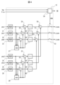
図1は、本発明の実施例1に係る3相PWMインバータの制御装置の一例を示す図である。
図1に示すPWMインバータ制御装置は、以下の構成要素を備える。
・第1のPWMモードに対応し、出力電圧位相指令θと出力電圧振幅指令Ymrに基づいて±120度離れた3相変調波を生成する変調波生成回路1、2および3
・第2のPWMモードに対応し、出力電圧位相指令θと出力電圧振幅指令Ymrに基づいて±120度離れた3相変調波を生成する変調波生成回路4、5および6
・変調波生成回路1、2および3の出力をそれぞれ入力し、第1のPWMモードに対応した搬送波と比較してゲートパルス信号GPU1とGNU1、GPV1とGNV1およびGPW1とGNW1をそれぞれ出力するパルス生成回路8、9および10
・変調波生成回路4、5および6の出力をそれぞれ入力し、第2のPWMモードに対応した搬送波と比較してゲートパルス信号GPU2とGNU2、GPV2とGNV2およびGPW2とGNW2をそれぞれ出力するパルス生成回路11、12および13
・出力電圧振幅指令Ymrと出力周波数指令Finvに基づいて、PWMモード選択信号SWを出力するPWMモード選択回路14
・PWMモード選択信号SWに基づき、パルス生成回路8、9および10とパルス生成回路11、12および13の出力を切り替えて、PWMインバータのゲートパルス信号GPU~GNWを出力するパルス切替回路7
The PWM inverter control device shown in FIG. 1 has the following components.
Modulated
Modulated
・Pulse generation for inputting outputs of modulated
・Pulse generation for inputting outputs of modulated
A PWM
A
次に、第1のPWMモードに対応した変調波生成回路1、2および3の動作例を示す。
変調波生成回路1、2および3それぞれは、[式5]に示すように、出力電圧振幅指令Ymrより関数A1を用いて変調波振幅a1を求め、この変調波振幅a1と出力電圧位相指令θに対して±120度離れた位相におけるsin関数との積により、3相変調波ymu1、ymv1およびymw1を生成する。
[式5] a1=A1(Ymr)
ymu1=a1×sin(θ)
ymv1=a1×sin(θ-2π/3)
ymw1=a1×sin(θ+2π/3)Next, an operation example of the modulated
Each of the modulated
[Expression 5] a1=A1(Ymr)
ymu1=a1×sin(θ)
ymv1=a1×sin(θ−2π/3)
ymw1=a1×sin(θ+2π/3)
ここで、関数A1は、第1のPWMモードのパルス数が十分多く、かつ出力電圧振幅指令Ymrが正弦波変調となる領域(過変調ではない領域、すなわち非飽和領域)では、変調波振幅a1は出力電圧振幅指令Ymrに比例するとみなして、a1=A1(Ymr)≒4/π×Ymrと近似できる。 Here, the function A1 has a sufficiently large number of pulses in the first PWM mode, and the modulated wave amplitude a1 is proportional to the output voltage amplitude command Ymr, and can be approximated as a1=A1(Ymr)≈4/π×Ymr.
しかし、変調波が飽和する過変調領域においては、線形近似が成立せず、変調波振幅a1と出力電圧振幅指令Ymrとの関係は非線形特性になるので、この非線形特性を関数A1として実装する。 However, in the overmodulated region where the modulated wave is saturated, the linear approximation does not hold, and the relationship between the modulated wave amplitude a1 and the output voltage amplitude command Ymr becomes non-linear. Therefore, this non-linear characteristic is implemented as the function A1.
また、本発明が対象とする電力変換装置(インバータ装置)においては、パルス数が十分でなく、正弦波変調領域であっても近似が成立しない場合がある。この場合には、変調波振幅a1と、実際の第1のPWMモードにおけるPWM波形をフーリエ積分して求めた実際の出力電圧振幅との関係を求め、この逆関数を関数A1として実装する。 In addition, in the power conversion device (inverter device) targeted by the present invention, the number of pulses may not be sufficient, and approximation may not hold even in the sinusoidal modulation region. In this case, the relationship between the modulated wave amplitude a1 and the actual output voltage amplitude obtained by Fourier integration of the actual PWM waveform in the first PWM mode is obtained, and this inverse function is implemented as the function A1.
同様に、第2のPWMモードに対応した変調波生成回路4、5および6それぞれも、[式6]に示すように、出力電圧振幅指令Ymrより関数A2を用いて変調波振幅a2を求め、この変調波振幅a2と出力電圧位相指令θに対して±120度離れた位相におけるsin関数との積により、3相変調波ymu2、ymv2およびymw2を生成する。
[式6] a2=A2(Ymr)
ymu2=a2×sin(θ)
ymv2=a2×sin(θ-2π/3)
ymw2=a2×sin(θ+2π/3)
ここで、関数A2は、関数A1と同様にして求める。Similarly, each of the modulated
[Expression 6] a2=A2(Ymr)
ymu2=a2*sin([theta])
ymv2=a2×sin(θ−2π/3)
ymw2=a2×sin(θ+2π/3)
Here, the function A2 is obtained in the same manner as the function A1.
第1のPWMモードに対応したパルス生成回路8、9および10は、第1のPWMモードの3相変調波ymu1、ymv1およびymw1を入力し、第1のPWMモードに対応した搬送波と比較して、PWMのゲートパルス信号GPU1とGNU1、GPV1とGNV1およびGPW1とGNW1を出力する。一般的に、パルス生成回路8、9および10の搬送波位相は同位相である。
また、3相各相のPWMのゲートパルス信号として、U相のGPU1とGNU1、V相のGPV1とGNV1およびW相のGPW1とGNW1は、それぞれアーム短絡を防止するためのデッドタイム(両方ともオフしている期間)を除き、いずれかの信号がオンしている相補信号である。 In addition, as PWM gate pulse signals for each of the three phases, U-phase GPU1 and GNU1, V-phase GPV1 and GNV1, and W-phase GPW1 and GNW1 are set to dead time (both off) to prevent arm short-circuiting. It is a complementary signal in which one of the signals is on except for the period when the signal is on.
第2のPWMモードに対応したパルス生成回路11、12および13は、第2のPWMモードの3相変調波ymu2、ymv2およびymw2を入力し、第2のPWMモードに対応した搬送波と比較してPWMのゲートパルス信号GPU2とGNU2、GPV2とGNV2およびGPW2とGNW2を出力する。
The
先の第1のPWMモードに対応したパルス生成回路8、9および10と同様に、パルス生成回路11、12および13の搬送波位相も一般的に同位相で、3相各相のPWMのゲートパルス信号として、U相のGPU2とGNU2、V相のGPV2とGNV2およびW相のGPW2とGNW2は、それぞれアーム短絡を防止するためのデッドタイム(両方ともオフしている期間)を除き、いずれかの信号がオンしている相補信号である。
Similarly to the
図2は、実施例1に係るPWMモード選択回路14の構成の一例を示す図である。
図2に示すPWMモード選択回路14は、以下の構成要素を備える。
・第1のPWMモードの3相変調波ymu1、ymv1およびymw1を入力し、それぞれ第1のPWM波形を出力するPWM波形演算器21、22および23
・第2のPWMモードの3相変調波ymu2、ymv2およびymw2を入力し、それぞれ第2のPWM波形を出力するPWM波形演算器24、25および26
・PWM波形演算器21、22および23の出力を入力し、第1のPWM波形の平均値を求める平均値演算器27
・PWM波形演算器24、25および26の出力を入力し、第2のPWM波形の平均値を求める平均値演算器28
・PWM波形演算器21、22および23の出力から、平均値演算器27の出力を差し引く減算器29、30および31
・PWM波形演算器24、25および26の出力から、平均値演算器28の出力を差し引く減算器32、33および34
・減算器29、30および31の出力をそれぞれ積分する積分器35、36および37
・減算器32、33および34の出力をそれぞれ積分する積分器38、39および40
・積分器35、36および37の出力と積分器38、39および40の出力をそれぞれ比較し、第1のPWMモード側の積分器(35、36および37)と第2のPWMモード側の積分器(38、39および40)のそれぞれ対応する2つ積分器の出力値が一致もしくはその偏差が許容範囲内に収まる場合は真、そうでない場合は偽を出力する比較器41、42および43
・比較器41、42および43の出力の論理積を求める論理積(AND)ゲート44
・出力電圧振幅指令Ymr、出力周波数指令Finvおよび論理積ゲート44の出力により、PWMモード選択信号SWを出力するPWMモード選択信号生成器45FIG. 2 is a diagram showing an example of the configuration of the PWM
The PWM
・
・
・
・
・
・
Comparing the outputs of the
and a logical product (AND)
A PWM mode
ここで、PWMモード選択信号生成器45は、出力電圧振幅指令Ymrおよび出力周波数指令Finvに基づいて、第1のPWMモードまたは第2のPWMモードを選択するPWMモード選択信号SWを、論理積ゲート44の出力が真である場合に切り替えて出力する。また、2つのPWMモード間を短期間で往来しないように、2つのPWMモード間の遷移領域にはヒステリシス幅を設ける。
Here, the PWM mode
以上のように、PWMモード選択信号SWの切替えに当たって、論理積ゲート44の出力が真である場合とは、比較器41、42および43の出力が全て真となるタイミングであって、すなわち、第1のPWMモードに対応する第1のPWM波形の積分値(すなわち電圧積分値)と第2のPWMモードに対応する第2のPWM波形の積分値(すなわち電圧積分値)とが3相全ての相で一致するか許容範囲内の差であるから、PWMモードの切替えにおいて、モータ電流の跳ね上がりを抑制することが可能となる。
As described above, in switching the PWM mode selection signal SW, when the output of the AND
次に、本発明の実施例2について説明する。
図3は、本発明の実施例2に係る3相PWMインバータの制御装置の一例を示す図である。
図3に示すPWMインバータ制御装置は、以下の構成要素を備える。ただし、図1に示す実施例1に係る3相PWMインバータの制御装置と同じ構成要素の説明は省略し、異なる構成要素についてのみ説明する。
・出力電圧振幅指令Ymrと出力周波数指令Finvに基づいてPWMモード選択信号SWと変調率補正量Δymu、ΔymvおよびΔymwを出力するPWMモード選択回路15
・変調波生成回路1、2および3の出力ymu1、ymv1およびymw1それぞれに対して、PWMモード選択回路15が出力する変調率補正量Δymu、ΔymvおよびΔymwを加算する加算器16、17および18Next, Example 2 of the present invention will be described.
The PWM inverter control device shown in FIG. 3 has the following components. However, descriptions of the same components as those of the three-phase PWM inverter control device according to the first embodiment shown in FIG. 1 will be omitted, and only different components will be described.
A PWM
また、パルス生成回路8、9および10それぞれは、変調波生成回路1、2および3の出力ymu1、ymv1およびymw1ではなく加算器16、17および18のそれぞれの出力を入力し、第1のPWMモードに対応した搬送波と比較してゲートパルス信号GPU1とGNU1、GPV1とGNV1およびGPW1とGNW1を出力する。
Further, the
図4は、実施例2に係るPWMモード選択回路15の構成の一例を示す図である。
図4に示すPWMモード選択回路15が備える構成要素について、以下では、図2に示す実施例1に係るPWMモード選択回路14と異なる部分についてのみ説明し、同じ部分についての説明は省略する。
・積分器35、36および37の出力と積分器38、39および40の出力との差分をそれぞれ求める減算器50、51および52
・出力電圧振幅指令Ymrと出力周波数指令Finvにより、PWMモード選択信号SWおよびPWMモード切替信号CHGを出力するPWMモード選択信号生成器54
・PWMモード切替信号CHGが有効のときは、減算器50、51および52の出力を変調率補正量Δymu、ΔymvおよびΔymwとして出力し、PWMモード切替信号CHGが無効のときはゼロを出力するスイッチ53FIG. 4 is a diagram showing an example of the configuration of the PWM
4. Only the components of the PWM
-
A PWM mode
A switch that outputs the outputs of the
また、PWMモード選択信号生成器54は、出力電圧振幅指令Ymrと出力周波数指令Finvに応じて、第1のPWMモードもしくは第2のPWMモードを選択するPWMモード選択信号SWを出力するが、2つのPWMモード間を短期間で往来しないように、2つのPWMモード間の遷移領域にはヒステリシス幅を設ける。さらに、PWMモード切替信号CHGは、通常は無効であり、第1のPWMモードから第2のPWMモードに切り替わる直前のみ有効となる。
Also, the PWM mode
図11は、本発明の実施例2による動作例(出力電圧積分値)の一例を示す図である。
図11では、PWMモード選択信号SWは、位相60度以前はLowレベルであって、第1のPWMモードである同期PWMIである、また、位相60度以後はHighレベルとなって、第2のPWMモードである同期PWMIIであることを示す。
また、PWMモード切替信号CHGは、通常はLowレベルであり無効であることを示し、位相60度の直前のみHighレベルとなって有効であることを示す。FIG. 11 is a diagram showing an operation example (output voltage integral value) according to the second embodiment of the present invention.
In FIG. 11, the PWM mode selection signal SW is Low level before
In addition, the PWM mode switching signal CHG is normally Low level indicating that it is invalid, and becomes High level only immediately before the phase of 60 degrees, indicating that it is valid.
図11において、位相60度の時点で、同期PWMIから同期PWMIIにPWMモードの切替えを行った際の電圧積分値を実線で示す。比較のために、本発明の実施例2を適用しなかった場合の電圧積分値を点線で示す。
本発明の実施例2を適用しなかった場合、図10に示したように、U相電圧積分値は負方向に偏り、V相電圧積分値は正方向に偏っていた。一方、図11に示すように、実施例2に係る構成により、位相60度の時点で、PWMモードの切替え直前に、U相では電圧積分値を正方向に補正することによって、U相電圧積分値のアンバランスを解消している。同様に、V相については、電圧積分値を負方向に補正することによって、V相電圧積分値のアンバランスを解消している。なお、W相は、位相60度では電圧積分値が一致しているので、補正なしとなる。In FIG. 11, the solid line indicates the voltage integration value when the PWM mode is switched from synchronous PWMI to synchronous PWMII at the point of
When the second embodiment of the present invention was not applied, as shown in FIG. 10, the U-phase voltage integral value was biased in the negative direction, and the V-phase voltage integral value was biased in the positive direction. On the other hand, as shown in FIG. 11, according to the configuration according to the second embodiment, at the point of
なお、実施例2では、同期PWMIから同期PWMIIへの切替え直前に補正量を加えている。これは、実施例2では、同期PWMIの方が同期PWMIIよりも同期パルス数が多いので、パルス数が多い側で補正量を加えた方が、より正確に電圧積分値をコントロールできるためである。 In the second embodiment, the correction amount is added immediately before switching from synchronous PWMI to synchronous PWMII. This is because, in the second embodiment, since synchronous PWMI has more synchronous pulses than synchronous PWMII, adding a correction amount on the side with a larger number of pulses enables more accurate control of the voltage integral value. .
図13は、本発明を適用した場合のモータ電流波形を示す図である。図8に示すモータ電流波形と異なり、同期PWMIから同期PWMIIへの切替えはスムーズに行われ、モータ電流の跳ね上がりは起きていない。
なお、同期PWMIの区間に比べて、同期PWMIIの区間の方が電流振幅が大きくなっているのは、同期PWMIに比べて同期PWMIIの方は同期パルス数が減っていることから、スイッチングリップルが大きくなっているためである。FIG. 13 is a diagram showing motor current waveforms when the present invention is applied. Unlike the motor current waveform shown in FIG. 8, the switching from synchronous PWMI to synchronous PWMII is performed smoothly, and the motor current does not jump up.
The reason why the current amplitude is larger in the synchronous PWMII section than in the synchronous PWMI section is that the number of synchronous pulses is smaller in the synchronous PWMII section than in the synchronous PWMI section. This is because they are getting bigger.
図5は、図3に示す実施例2に係るPWMモード選択回路15の構成の別の一例を示す図である。
図5に示すPWMモード選択回路15は、PWMモード選択信号生成器55が、PWMモード選択信号SWおよびPWMモード切替信号CHGを、出力電圧振幅指令Ymrと出力周波数指令Finvと減算器50、51および52の出力との3つの信号に基づいて出力する点において、図4に示すPWMモード選択回路15のPWMモード選択信号生成器54と異なる。FIG. 5 is a diagram showing another example of the configuration of the PWM
PWM
PWMモード選択信号生成器55は、出力電圧振幅指令Ymrと出力周波数指令Finvとに応じて、第1のPWMモードもしくは第2のPWMモードを選択する信号を出力する。ただしその際に、2つのPWMモード間を短期間で往来しないように、2つのPWMモード間の遷移領域にはヒステリシス幅を設ける。さらに、減算器50、51および52の出力の中でいずれか一相がゼロまたはゼロとみなせる許容範囲内に収まる場合にのみ、PWMモード選択信号SWを切り替えるものである。また、PWMモード切替信号CHGは、通常は無効であり、第1のPWMモードから第2のPWMモードに切り替わる直前にのみ有効となる。
The PWM mode
図12は、位相ごとの変調率補正量を示す表である。
図9に示すように、3相の電圧積分値の内、60度の整数倍の位相でいずれかの相は必ずゼロクロスする。3相の電圧積分値の総和は必ずゼロになるので、残りの2相の和も必ずゼロになる。PWMモードの切替え前後のいずれのPWMモードでも同様であるから、電圧積分値の差である変調率補正量もいずれか一相はゼロになり、残りの2相の和も必ずゼロとなる。ここで、変調率補正量については、+ΔVと-ΔVとする。FIG. 12 is a table showing the modulation factor correction amount for each phase.
As shown in FIG. 9, one of the three-phase integrated voltage values always crosses zero at a phase integral multiple of 60 degrees. Since the sum of the voltage integral values of the three phases is always zero, the sum of the remaining two phases is also always zero. Since the same is true in any PWM mode before and after PWM mode switching, the modulation factor correction amount, which is the difference in voltage integral value, is zero for any one phase, and the sum of the remaining two phases is always zero. Here, the modulation factor correction amounts are +ΔV and −ΔV.
図12に示すように、例えば、位相60度のとき、W相の変調率補正量はゼロとなり、U相の変調率補正量は+ΔV、V相の変調率補正量は-ΔVとなる。このように、60度の整数倍の位相では、変調率補正量はゼロまたは±ΔVのいずれかの値となる。 As shown in FIG. 12, for example, when the phase is 60 degrees, the W-phase modulation factor correction amount is zero, the U-phase modulation factor correction amount is +ΔV, and the V-phase modulation factor correction amount is −ΔV. In this way, the modulation factor correction amount is either zero or ±ΔV at the phases of integral multiples of 60 degrees.
図9と照らし合わせると、U相の電圧積分値は、位相0度ではゼロであり、位相60度における2つのPWMモードの電圧積分値の差が変調率補正量ΔVとなる。これは、電圧積分値の演算においては、無限時間に渡って積分動作を行う必要はなく、60度ごとにゼロの状態から積分を行えばよいことを示している。積分器が長時間動作すると、わずかな演算誤差が蓄積してアンバランスの要因になりかねないが、本発明の構成においては、積分器を60度ごとにリセットすることでその問題を解消することができる。 When compared with FIG. 9, the U-phase voltage integral value is zero at a phase of 0 degrees, and the difference between the two PWM mode voltage integral values at a phase of 60 degrees is the modulation factor correction amount ΔV. This indicates that in the calculation of the voltage integral value, it is not necessary to perform the integration operation over an infinite time, and it is sufficient to perform the integration from the zero state every 60 degrees. If the integrator operates for a long period of time, slight calculation errors may accumulate and cause unbalance. However, in the configuration of the present invention, the problem can be solved by resetting the integrator every 60 degrees. can be done.
1、2、3 第1のPWMモードの変調波生成回路
4、5、6 第2のPWMモードの変調波生成回路
7 パルス切替回路(セレクタ)
8、9、10 第1のPWMモードのパルス生成回路
11、12、13 第2のPWMモードのパルス生成回路
14、15 PWMモード選択回路
16、17、18 加算器
21、22、23 第1のPWMモードのPWM波形演算器
24、25、26 第2のPWMモードのPWM波形演算器
27、28 平均値演算器
29、30、31、32、33、34 減算器
35、36、37、38、39、40 積分器
41、42、43 比較器
44 論理積(AND)ゲート
45 PWMモード選択信号生成器
50、51、52 加算器
53 スイッチ
54、55 PWMモード選択信号生成器
81 平滑化コンデンサ
82、84、86 3相ブリッジの上アームの半導体スイッチング素子
83、85、87 3相ブリッジの下アームの半導体スイッチング素子
88 モータ(交流電動機)
90、91、92 抵抗R
93、94、95 インダクタンスL
96、97、98 速度起電力の等価電源1, 2, 3 first PWM mode modulated
8, 9, 10 first PWM mode
90, 91, 92 resistor R
93, 94, 95 Inductance L
96, 97, 98 Speed electromotive force equivalent power supply
Claims (10)
前記第1の変調波と前記第1のPWMモードに対応した搬送波とを比較して第1のPWMパルスを生成する第1のパルス生成回路と、
前記第2の変調波と前記第2のPWMモードに対応した搬送波とを比較して第2のPWMパルスを生成する第2のパルス生成回路と、
前記PWMインバータの出力周波数指令および前記出力電圧振幅指令に基づいて前記第1または前記第2のPWMモードのいずれかを選択するPWMモード選択信号を生成するPWMモード選択回路と、
前記PWMモード選択信号に応じて前記第1のPWMパルスと前記第2のPWMパルスとを切り替えてPWMインバータの駆動パルスとするパルス切替回路と
を備え、
前記PWMモード選択回路は、
前記PWMモード選択信号を、前記第1のPWMパルスを前記駆動パルスとした場合の前記PWMインバータの出力電圧積分値と、前記第2のPWMパルスを前記駆動パルスとした場合の前記PWMインバータの出力電圧積分値とが一致するタイミングで生成する
ことを特徴とするPWMインバータ制御装置。a modulated wave generation circuit for generating a first modulated wave corresponding to the first PWM mode and a second modulated wave corresponding to the second PWM mode based on the output voltage phase command and the output voltage amplitude command of the PWM inverter; ,
a first pulse generation circuit that compares the first modulated wave with a carrier wave corresponding to the first PWM mode to generate a first PWM pulse;
a second pulse generation circuit that compares the second modulated wave with a carrier wave corresponding to the second PWM mode to generate a second PWM pulse;
a PWM mode selection circuit that generates a PWM mode selection signal that selects either the first or second PWM mode based on the output frequency command and the output voltage amplitude command of the PWM inverter;
a pulse switching circuit that switches between the first PWM pulse and the second PWM pulse according to the PWM mode selection signal and uses the PWM inverter as a driving pulse;
The PWM mode selection circuit
The PWM mode selection signal is the output voltage integral value of the PWM inverter when the first PWM pulse is the driving pulse, and the output of the PWM inverter when the second PWM pulse is the driving pulse. A PWM inverter control device, characterized in that it is generated at a timing that coincides with a voltage integral value.
前記第1の変調波と前記第1のPWMモードに対応した搬送波とを比較して第1のPWMパルスを生成する第1のパルス生成回路と、
前記第2の変調波と前記第2のPWMモードに対応した搬送波とを比較して第2のPWMパルスを生成する第2のパルス生成回路と、
前記PWMインバータの出力周波数指令および前記出力電圧振幅指令に基づいて前記第1または前記第2のPWMモードのいずれかを選択するPWMモード選択信号を生成するPWMモード選択回路と、
前記PWMモード選択信号に応じて前記第1のPWMパルスと前記第2のPWMパルスとを切り替えて前記PWMインバータの駆動パルスとするパルス切替回路と
を備え、
前記PWMモード選択回路は、
前記第1の変調波から第1のPWM波形を演算し当該第1のPWM波形を積分する第1の演算器と、前記第2の変調波から第2のPWM波形を演算し当該第2のPWM波形を積分する第2の演算器とを有し、
前記PWMモード選択信号を、前記第1の演算器の出力と前記第2の演算器の出力とが一致するタイミングで生成する
ことを特徴とするPWMインバータ制御装置。a modulated wave generation circuit for generating a first modulated wave corresponding to the first PWM mode and a second modulated wave corresponding to the second PWM mode based on the output voltage phase command and the output voltage amplitude command of the PWM inverter; ,
a first pulse generation circuit that compares the first modulated wave with a carrier wave corresponding to the first PWM mode to generate a first PWM pulse;
a second pulse generation circuit that compares the second modulated wave with a carrier wave corresponding to the second PWM mode to generate a second PWM pulse;
a PWM mode selection circuit that generates a PWM mode selection signal that selects either the first or second PWM mode based on the output frequency command and the output voltage amplitude command of the PWM inverter;
a pulse switching circuit that switches between the first PWM pulse and the second PWM pulse in response to the PWM mode selection signal to use as a drive pulse for the PWM inverter;
The PWM mode selection circuit
A first calculator that calculates a first PWM waveform from the first modulated wave and integrates the first PWM waveform, and a second PWM waveform that is calculated from the second modulated wave and the second and a second calculator that integrates the PWM waveform,
A PWM inverter control device, wherein the PWM mode selection signal is generated at a timing when the output of the first computing unit and the output of the second computing unit match.
前記PWMインバータは、3相PWMインバータであり、
前記第1および前記第2の変調波は、それぞれ3相分の変調波であり、
前記第1の演算器は、前記第1の変調波から3相各相のPWM波形を求め、当該3相各相のPWM波形それぞれから当該3相各相のPWM波形の平均値を減算することで、前記第1のPWM波形を演算し、
前記第2の演算器は、前記第2の変調波から3相各相のPWM波形を求め、当該3相各相のPWM波形それぞれから当該3相各相のPWM波形の平均値を減算することで、前記第2のPWM波形を演算し、
前記PWMモード選択信号は、前記第1の演算器の3相分の出力と前記第2の演算器の3相分の出力とが3相各相で全て一致するまたは許容範囲内の偏差であるタイミングで生成される
ことを特徴とするPWMインバータ制御装置。The PWM inverter control device according to claim 2,
The PWM inverter is a three-phase PWM inverter,
each of the first and second modulated waves is a modulated wave for three phases;
The first calculator obtains a PWM waveform of each of the three phases from the first modulated wave, and subtracts an average value of the PWM waveform of each of the three phases from each of the PWM waveforms of the three phases. to calculate the first PWM waveform,
The second calculator obtains a PWM waveform of each of the three phases from the second modulated wave, and subtracts an average value of the PWM waveform of each of the three phases from each of the PWM waveforms of the three phases. to calculate the second PWM waveform,
The PWM mode selection signal is such that the three-phase outputs of the first computing unit and the three-phase outputs of the second computing unit all match in each of the three phases or have a deviation within an allowable range. A PWM inverter control device characterized in that it is generated with timing.
変調率補正量を所定のタイミングで加算した前記第1の変調波と前記第1のPWMモードに対応した搬送波とを比較して第1のPWMパルスを生成する第1のパルス生成回路と、
前記第2の変調波と前記第2のPWMモードに対応した搬送波とを比較して第2のPWMパルスを生成する第2のパルス生成回路と、
前記PWMインバータの出力周波数指令および前記出力電圧振幅指令に基づいて前記第1または前記第2のPWMモードのいずれかを選択するPWMモード選択信号および前記変調率補正量を生成するPWMモード選択回路と、
前記PWMモード選択信号に応じて前記第1のPWMパルスと前記第2のPWMパルスとを切り替えてPWMインバータの駆動パルスとするパルス切替回路と
を備え、
前記PWMモード選択回路は、
前記第1の変調波から第1のPWM波形を演算し当該第1のPWM波形を積分する第1の演算器と、前記第2の変調波から第2のPWM波形を演算し当該第2のPWM波形を積分する第2の演算器と、前記第1の演算器の出力と前記第2の演算器の出力との差に応じた前記変調率補正量を出力する第3の演算器とを有し、
前記所定のタイミングは、前記PWMモード選択信号に応じて前記第1のPWMモードと前記第2のPWMモードとを切り替える直前のタイミングである
ことを特徴とするPWMインバータ制御装置。a modulated wave generation circuit for generating a first modulated wave corresponding to the first PWM mode and a second modulated wave corresponding to the second PWM mode based on the output voltage phase command and the output voltage amplitude command of the PWM inverter; ,
a first pulse generation circuit that compares the first modulated wave obtained by adding the modulation factor correction amount at a predetermined timing with a carrier wave corresponding to the first PWM mode to generate a first PWM pulse;
a second pulse generation circuit that compares the second modulated wave with a carrier wave corresponding to the second PWM mode to generate a second PWM pulse;
a PWM mode selection circuit for generating a PWM mode selection signal for selecting either the first or second PWM mode based on the output frequency command and the output voltage amplitude command of the PWM inverter and the modulation factor correction amount; ,
a pulse switching circuit that switches between the first PWM pulse and the second PWM pulse according to the PWM mode selection signal and uses the PWM inverter as a driving pulse;
The PWM mode selection circuit
A first calculator that calculates a first PWM waveform from the first modulated wave and integrates the first PWM waveform, and a second PWM waveform that is calculated from the second modulated wave and the second a second computing unit that integrates a PWM waveform; and a third computing unit that outputs the modulation factor correction amount according to the difference between the output of the first computing unit and the output of the second computing unit. have
The PWM inverter control device, wherein the predetermined timing is timing immediately before switching between the first PWM mode and the second PWM mode according to the PWM mode selection signal.
前記PWMインバータは、3相PWMインバータであり、
前記第1および前記第2の変調波は、それぞれ3相分の変調波であり、
前記第1の演算器は、前記第1の変調波から3相各相のPWM波形を求め、当該3相各相のPWM波形それぞれから当該3相各相のPWM波形の平均値を減算することで、前記第1のPWM波形を演算し、
前記第2の演算器は、前記第2の変調波から3相各相のPWM波形を求め、当該3相各相のPWM波形それぞれから当該3相各相のPWM波形の平均値を減算することで、前記第2のPWM波形を演算し、
前記第3の演算器は、3相の前記第1の演算器の前記出力それぞれから3相の前記第2の演算器の前記出力を減算して3相の前記変調率補正量を出力する
ことを特徴とするPWMインバータ制御装置。The PWM inverter control device according to claim 4,
The PWM inverter is a three-phase PWM inverter,
each of the first and second modulated waves is a modulated wave for three phases;
The first calculator obtains a PWM waveform of each of the three phases from the first modulated wave, and subtracts an average value of the PWM waveform of each of the three phases from each of the PWM waveforms of the three phases. to calculate the first PWM waveform,
The second calculator obtains a PWM waveform of each of the three phases from the second modulated wave, and subtracts an average value of the PWM waveform of each of the three phases from each of the PWM waveforms of the three phases. to calculate the second PWM waveform,
The third arithmetic unit subtracts the outputs of the second arithmetic unit of three phases from the outputs of the first arithmetic unit of three phases to output the modulation factor correction amounts of three phases. A PWM inverter control device characterized by:
前記PWMモード選択回路は、前記3相のいずれか1相の前記変調率補正量がゼロまたはゼロとみなせる許容範囲内に収まる場合に、前記PWMモード選択信号を生成する
ことを特徴とするPWMインバータ制御装置。The PWM inverter control device according to claim 5,
The PWM inverter, wherein the PWM mode selection circuit generates the PWM mode selection signal when the modulation factor correction amount of any one of the three phases is zero or falls within an allowable range that can be regarded as zero. Control device.
前記第1のPWMモードと前記第2のPWMモードとの遷移領域にはヒステリシス幅を設ける
ことを特徴とするPWMインバータ制御装置。The PWM inverter control device according to any one of claims 1 to 6,
A PWM inverter control device, wherein a hysteresis width is provided in a transition region between the first PWM mode and the second PWM mode.
前記第1の変調波と前記第1のPWMモードに対応した搬送波とを比較して第1のPWMパルスを生成し、前記第2の変調波と前記第2のPWMモードに対応した搬送波とを比較して第2のPWMパルスを生成するパルス生成ステップと、
前記PWMインバータの出力周波数指令および前記出力電圧振幅指令に基づいて前記第1もしくは前記第2のPWMモードのいずれかを選択するPWMモード選択信号を、前記第1のPWMパルスを前記PWMインバータの駆動パルスとした場合の前記PWMインバータの出力電圧積分値と、前記第2のPWMパルスを前記PWMインバータの駆動パルスとした場合の前記PWMインバータの出力電圧積分値とが一致するタイミングで生成するPWMモード選択ステップと、
前記PWMモード選択信号に応じて前記第1のPWMパルスと前記第2のPWMパルスとを切り替えて前記PWMインバータを駆動する駆動ステップと
を有するPWMインバータ制御方法。a modulated wave generation step of generating a first modulated wave corresponding to the first PWM mode and a second modulated wave corresponding to the second PWM mode based on the output voltage phase command and the output voltage amplitude command of the PWM inverter; ,
comparing the first modulated wave with a carrier wave corresponding to the first PWM mode to generate a first PWM pulse, and comparing the second modulated wave with the carrier wave corresponding to the second PWM mode; a pulse generation step of comparing to generate a second PWM pulse;
A PWM mode selection signal for selecting either the first or the second PWM mode based on the output frequency command and the output voltage amplitude command of the PWM inverter, and the first PWM pulse for driving the PWM inverter. A PWM mode generated at timing at which the output voltage integral value of the PWM inverter when the second PWM pulse is used as a pulse coincides with the output voltage integral value of the PWM inverter when the second PWM pulse is used as the driving pulse of the PWM inverter. a selection step;
and a driving step of switching between the first PWM pulse and the second PWM pulse according to the PWM mode selection signal to drive the PWM inverter.
前記第1の変調波と前記第1のPWMモードに対応した搬送波とを比較して第1のPWMパルスを生成し、前記第2の変調波と前記第2のPWMモードに対応した搬送波とを比較して第2のPWMパルスを生成するパルス生成ステップと、
前記PWMインバータの出力周波数指令および前記出力電圧振幅指令に基づいて前記第1または前記第2のPWMモードのいずれかを選択するPWMモード選択信号を生成するPWMモード選択ステップと、
前記PWMモード選択信号に応じて前記第1のPWMパルスと前記第2のPWMパルスとを切り替えて前記PWMインバータを駆動する駆動ステップと
を有し、
前記PWMモード選択ステップは、
前記第1の変調波から算出した第1のPWM波形を積分して第1の積分値を演算し、前記第2の変調波から算出した第2のPWM波形を積分して第2の積分値を演算する演算ステップと、
前記第1の積分値と前記第2の積分値とが一致するタイミングで前記PWMモード選択信号を生成するステップとから成る
ことを特徴とするPWMインバータ制御方法。a modulated wave generation step of generating a first modulated wave corresponding to the first PWM mode and a second modulated wave corresponding to the second PWM mode based on the output voltage phase command and the output voltage amplitude command of the PWM inverter; ,
comparing the first modulated wave with a carrier wave corresponding to the first PWM mode to generate a first PWM pulse, and comparing the second modulated wave with the carrier wave corresponding to the second PWM mode; a pulse generation step of comparing to generate a second PWM pulse;
a PWM mode selection step of generating a PWM mode selection signal for selecting either the first or second PWM mode based on the output frequency command and the output voltage amplitude command of the PWM inverter;
a driving step of switching between the first PWM pulse and the second PWM pulse according to the PWM mode selection signal to drive the PWM inverter;
The PWM mode selection step includes:
calculating a first integral value by integrating a first PWM waveform calculated from the first modulated wave; and calculating a second integral value by integrating a second PWM waveform calculated from the second modulated wave a computing step of computing
and generating the PWM mode selection signal at a timing when the first integrated value and the second integrated value match.
前記第1の変調波と前記第1のPWMモードに対応した搬送波とを比較して第1のPWMパルスを生成し、前記第2の変調波と前記第2のPWMモードに対応した搬送波とを比較して第2のPWMパルスを生成するパルス生成ステップと、
前記PWMインバータの出力周波数指令および前記出力電圧振幅指令に基づいて前記第1または前記第2のPWMモードのいずれかを選択するPWMモード選択信号を生成するPWMモード選択ステップと、
前記第1の変調波から算出した第1のPWM波形を積分して第1の積分値を演算し、前記第2の変調波から算出した第2のPWM波形を積分して第2の積分値を演算し、前記第1の積分値と前記第2の積分値との差を変調率補正量として演算し、当該変調率補正量を、前記第1の変調波に対して、前記PWMモード選択信号に応じて前記第1のPWMモードと前記第2のPWMモードとを切り替える直前のタイミングで加算する演算ステップと、
前記PWMモード選択信号に応じて前記第1のPWMパルスと前記第2のPWMパルスとを切り替えて前記PWMインバータを駆動する駆動ステップと
を有するPWMインバータ制御方法。a modulated wave generation step of generating a first modulated wave corresponding to the first PWM mode and a second modulated wave corresponding to the second PWM mode based on the output voltage phase command and the output voltage amplitude command of the PWM inverter; ,
comparing the first modulated wave with a carrier wave corresponding to the first PWM mode to generate a first PWM pulse, and comparing the second modulated wave with the carrier wave corresponding to the second PWM mode; a pulse generation step of comparing to generate a second PWM pulse;
a PWM mode selection step of generating a PWM mode selection signal for selecting either the first or second PWM mode based on the output frequency command and the output voltage amplitude command of the PWM inverter;
calculating a first integral value by integrating a first PWM waveform calculated from the first modulated wave; and calculating a second integral value by integrating a second PWM waveform calculated from the second modulated wave and calculating the difference between the first integral value and the second integral value as a modulation factor correction amount, and applying the modulation factor correction amount to the first modulated wave in the PWM mode selection a calculation step of adding at a timing immediately before switching between the first PWM mode and the second PWM mode according to a signal;
and a driving step of switching between the first PWM pulse and the second PWM pulse according to the PWM mode selection signal to drive the PWM inverter.
Applications Claiming Priority (3)
| Application Number | Priority Date | Filing Date | Title |
|---|---|---|---|
| JP2019219012 | 2019-12-03 | ||
| JP2019219012 | 2019-12-03 | ||
| PCT/JP2020/044777 WO2021112108A1 (en) | 2019-12-03 | 2020-12-02 | Pwm inverter control device and control method |
Publications (2)
| Publication Number | Publication Date |
|---|---|
| JPWO2021112108A1 JPWO2021112108A1 (en) | 2021-06-10 |
| JP7328352B2 true JP7328352B2 (en) | 2023-08-16 |
Family
ID=76221651
Family Applications (1)
| Application Number | Title | Priority Date | Filing Date |
|---|---|---|---|
| JP2021562676A Active JP7328352B2 (en) | 2019-12-03 | 2020-12-02 | PWM inverter control device and control method |
Country Status (3)
| Country | Link |
|---|---|
| EP (1) | EP4071998A4 (en) |
| JP (1) | JP7328352B2 (en) |
| WO (1) | WO2021112108A1 (en) |
Citations (3)
| Publication number | Priority date | Publication date | Assignee | Title |
|---|---|---|---|---|
| JP2005348597A (en) | 1993-12-17 | 2005-12-15 | Hitachi Ltd | Controller for electric vehicle |
| WO2014174597A1 (en) | 2013-04-23 | 2014-10-30 | 三菱電機株式会社 | Control device for alternating current electric motor |
| JP2019103267A (en) | 2017-12-04 | 2019-06-24 | 日立オートモティブシステムズ株式会社 | Motor drive system |
Family Cites Families (6)
| Publication number | Priority date | Publication date | Assignee | Title |
|---|---|---|---|---|
| JPH08331856A (en) * | 1995-05-30 | 1996-12-13 | Toshiba Corp | Power converting apparatus |
| JP3276135B2 (en) | 1996-03-11 | 2002-04-22 | 株式会社東芝 | Power converter |
| JP3336588B2 (en) * | 1997-05-28 | 2002-10-21 | 株式会社日立製作所 | PWM pulse generator |
| JP2005086920A (en) * | 2003-09-09 | 2005-03-31 | Fuji Electric Systems Co Ltd | Method for controlling synchronous motor-driving device |
| JP5319205B2 (en) * | 2008-08-22 | 2013-10-16 | 株式会社豊田中央研究所 | Motor control device |
| JP6381497B2 (en) * | 2015-09-02 | 2018-08-29 | 三菱電機株式会社 | Power converter |
-
2020
- 2020-12-02 WO PCT/JP2020/044777 patent/WO2021112108A1/en unknown
- 2020-12-02 EP EP20896316.5A patent/EP4071998A4/en active Pending
- 2020-12-02 JP JP2021562676A patent/JP7328352B2/en active Active
Patent Citations (3)
| Publication number | Priority date | Publication date | Assignee | Title |
|---|---|---|---|---|
| JP2005348597A (en) | 1993-12-17 | 2005-12-15 | Hitachi Ltd | Controller for electric vehicle |
| WO2014174597A1 (en) | 2013-04-23 | 2014-10-30 | 三菱電機株式会社 | Control device for alternating current electric motor |
| JP2019103267A (en) | 2017-12-04 | 2019-06-24 | 日立オートモティブシステムズ株式会社 | Motor drive system |
Also Published As
| Publication number | Publication date |
|---|---|
| JPWO2021112108A1 (en) | 2021-06-10 |
| WO2021112108A1 (en) | 2021-06-10 |
| EP4071998A1 (en) | 2022-10-12 |
| EP4071998A4 (en) | 2023-12-13 |
Similar Documents
| Publication | Publication Date | Title |
|---|---|---|
| EP0571755B1 (en) | Power converter for converting DC voltage into AC phase voltage having three levels of positive, zero and negative voltage | |
| JP5683760B2 (en) | Power converter | |
| WO2010082265A1 (en) | Power converting apparatus | |
| KR20080109878A (en) | Power converter | |
| JPH05227796A (en) | Controller for power converter | |
| CN112005482B (en) | Three-level power conversion device, control method for three-level power conversion device, and storage medium | |
| JP6178433B2 (en) | Power converter | |
| JP2016082786A (en) | Neutral point clamp type power conversion device and control method therefor | |
| CN104578810A (en) | Matrix converter | |
| JP2009201248A (en) | Clamp power conversion apparatus | |
| US11863098B2 (en) | Multi-level inverter | |
| JP7328352B2 (en) | PWM inverter control device and control method | |
| JPH02261063A (en) | Inverter device and driving system for ac motor | |
| JP3547117B2 (en) | Torque detection device and drive control device for AC motor | |
| JP4661197B2 (en) | Control method of voltage source inverter | |
| WO2021136677A1 (en) | Method for operating a power electronic converter device with floating cells | |
| JP4277360B2 (en) | 3-level inverter controller | |
| JP7251336B2 (en) | motor controller | |
| WO2022018841A1 (en) | Power conversion device and electric power steering device | |
| WO2024042942A1 (en) | Drive control apparatus and drive control method for rotating electrical machine | |
| JPH01298959A (en) | Pwm converter | |
| JP5863451B2 (en) | Power converter | |
| JP2023050505A (en) | power converter | |
| JP2003018851A (en) | Control method of direct frequency conversion circuit | |
| Li et al. | Performance comparison of a new current regulator for 3-level NPC inverter for sinusoidal and non-sinusoidal current tracking applications |
Legal Events
| Date | Code | Title | Description |
|---|---|---|---|
| A621 | Written request for application examination |
Free format text: JAPANESE INTERMEDIATE CODE: A621 Effective date: 20220519 |
|
| TRDD | Decision of grant or rejection written | ||
| A01 | Written decision to grant a patent or to grant a registration (utility model) |
Free format text: JAPANESE INTERMEDIATE CODE: A01 Effective date: 20230801 |
|
| A61 | First payment of annual fees (during grant procedure) |
Free format text: JAPANESE INTERMEDIATE CODE: A61 Effective date: 20230803 |
|
| R150 | Certificate of patent or registration of utility model |
Ref document number: 7328352 Country of ref document: JP Free format text: JAPANESE INTERMEDIATE CODE: R150 |