JP6949567B2 - Image forming device - Google Patents
Image forming device Download PDFInfo
- Publication number
- JP6949567B2 JP6949567B2 JP2017115267A JP2017115267A JP6949567B2 JP 6949567 B2 JP6949567 B2 JP 6949567B2 JP 2017115267 A JP2017115267 A JP 2017115267A JP 2017115267 A JP2017115267 A JP 2017115267A JP 6949567 B2 JP6949567 B2 JP 6949567B2
- Authority
- JP
- Japan
- Prior art keywords
- power
- power supply
- image forming
- forming apparatus
- inrush current
- Prior art date
- Legal status (The legal status is an assumption and is not a legal conclusion. Google has not performed a legal analysis and makes no representation as to the accuracy of the status listed.)
- Active
Links
Images


Classifications
-
- G—PHYSICS
- G03—PHOTOGRAPHY; CINEMATOGRAPHY; ANALOGOUS TECHNIQUES USING WAVES OTHER THAN OPTICAL WAVES; ELECTROGRAPHY; HOLOGRAPHY
- G03G—ELECTROGRAPHY; ELECTROPHOTOGRAPHY; MAGNETOGRAPHY
- G03G15/00—Apparatus for electrographic processes using a charge pattern
- G03G15/80—Details relating to power supplies, circuits boards, electrical connections
-
- H—ELECTRICITY
- H02—GENERATION; CONVERSION OR DISTRIBUTION OF ELECTRIC POWER
- H02M—APPARATUS FOR CONVERSION BETWEEN AC AND AC, BETWEEN AC AND DC, OR BETWEEN DC AND DC, AND FOR USE WITH MAINS OR SIMILAR POWER SUPPLY SYSTEMS; CONVERSION OF DC OR AC INPUT POWER INTO SURGE OUTPUT POWER; CONTROL OR REGULATION THEREOF
- H02M1/00—Details of apparatus for conversion
- H02M1/36—Means for starting or stopping converters
-
- H—ELECTRICITY
- H02—GENERATION; CONVERSION OR DISTRIBUTION OF ELECTRIC POWER
- H02M—APPARATUS FOR CONVERSION BETWEEN AC AND AC, BETWEEN AC AND DC, OR BETWEEN DC AND DC, AND FOR USE WITH MAINS OR SIMILAR POWER SUPPLY SYSTEMS; CONVERSION OF DC OR AC INPUT POWER INTO SURGE OUTPUT POWER; CONTROL OR REGULATION THEREOF
- H02M1/00—Details of apparatus for conversion
- H02M1/42—Circuits or arrangements for compensating for or adjusting power factor in converters or inverters
- H02M1/4208—Arrangements for improving power factor of AC input
- H02M1/4258—Arrangements for improving power factor of AC input using a single converter stage both for correction of AC input power factor and generation of a regulated and galvanically isolated DC output voltage
-
- H—ELECTRICITY
- H02—GENERATION; CONVERSION OR DISTRIBUTION OF ELECTRIC POWER
- H02M—APPARATUS FOR CONVERSION BETWEEN AC AND AC, BETWEEN AC AND DC, OR BETWEEN DC AND DC, AND FOR USE WITH MAINS OR SIMILAR POWER SUPPLY SYSTEMS; CONVERSION OF DC OR AC INPUT POWER INTO SURGE OUTPUT POWER; CONTROL OR REGULATION THEREOF
- H02M3/00—Conversion of dc power input into dc power output
- H02M3/22—Conversion of dc power input into dc power output with intermediate conversion into ac
- H02M3/24—Conversion of dc power input into dc power output with intermediate conversion into ac by static converters
- H02M3/28—Conversion of dc power input into dc power output with intermediate conversion into ac by static converters using discharge tubes with control electrode or semiconductor devices with control electrode to produce the intermediate ac
- H02M3/325—Conversion of dc power input into dc power output with intermediate conversion into ac by static converters using discharge tubes with control electrode or semiconductor devices with control electrode to produce the intermediate ac using devices of a triode or a transistor type requiring continuous application of a control signal
- H02M3/335—Conversion of dc power input into dc power output with intermediate conversion into ac by static converters using discharge tubes with control electrode or semiconductor devices with control electrode to produce the intermediate ac using devices of a triode or a transistor type requiring continuous application of a control signal using semiconductor devices only
- H02M3/33507—Conversion of dc power input into dc power output with intermediate conversion into ac by static converters using discharge tubes with control electrode or semiconductor devices with control electrode to produce the intermediate ac using devices of a triode or a transistor type requiring continuous application of a control signal using semiconductor devices only with automatic control of the output voltage or current, e.g. flyback converters
- H02M3/33523—Conversion of dc power input into dc power output with intermediate conversion into ac by static converters using discharge tubes with control electrode or semiconductor devices with control electrode to produce the intermediate ac using devices of a triode or a transistor type requiring continuous application of a control signal using semiconductor devices only with automatic control of the output voltage or current, e.g. flyback converters with galvanic isolation between input and output of both the power stage and the feedback loop
-
- G—PHYSICS
- G03—PHOTOGRAPHY; CINEMATOGRAPHY; ANALOGOUS TECHNIQUES USING WAVES OTHER THAN OPTICAL WAVES; ELECTROGRAPHY; HOLOGRAPHY
- G03G—ELECTROGRAPHY; ELECTROPHOTOGRAPHY; MAGNETOGRAPHY
- G03G15/00—Apparatus for electrographic processes using a charge pattern
- G03G15/50—Machine control of apparatus for electrographic processes using a charge pattern, e.g. regulating differents parts of the machine, multimode copiers, microprocessor control
- G03G15/5004—Power supply control, e.g. power-saving mode, automatic power turn-off
-
- Y—GENERAL TAGGING OF NEW TECHNOLOGICAL DEVELOPMENTS; GENERAL TAGGING OF CROSS-SECTIONAL TECHNOLOGIES SPANNING OVER SEVERAL SECTIONS OF THE IPC; TECHNICAL SUBJECTS COVERED BY FORMER USPC CROSS-REFERENCE ART COLLECTIONS [XRACs] AND DIGESTS
- Y02—TECHNOLOGIES OR APPLICATIONS FOR MITIGATION OR ADAPTATION AGAINST CLIMATE CHANGE
- Y02B—CLIMATE CHANGE MITIGATION TECHNOLOGIES RELATED TO BUILDINGS, e.g. HOUSING, HOUSE APPLIANCES OR RELATED END-USER APPLICATIONS
- Y02B70/00—Technologies for an efficient end-user side electric power management and consumption
- Y02B70/10—Technologies improving the efficiency by using switched-mode power supplies [SMPS], i.e. efficient power electronics conversion e.g. power factor correction or reduction of losses in power supplies or efficient standby modes
Landscapes
- Engineering & Computer Science (AREA)
- Power Engineering (AREA)
- Physics & Mathematics (AREA)
- General Physics & Mathematics (AREA)
- Microelectronics & Electronic Packaging (AREA)
- Direct Current Feeding And Distribution (AREA)
- Dc-Dc Converters (AREA)
- Rectifiers (AREA)
- Accessory Devices And Overall Control Thereof (AREA)
- Control Or Security For Electrophotography (AREA)
- Power Sources (AREA)
Description
本発明は、突入電流防止回路を有する画像形成装置の技術に関する。 The present invention relates to a technique for an image forming apparatus having an inrush current prevention circuit.
電気機器には、各負荷への給電のために交流電圧を直流電圧に変換するAC/DC電源が搭載されている。AC/DC電源(電源装置)は、商用電源からの交流電圧をダイオードブリッジを介して整流し、平滑コンデンサを介して平滑化する。その後、トランスを介して2次側のコンデンサを充電して直流電圧を生成する。2次側にはAC/DC電源の出力電圧を検知する回路を備えており、出力電圧が所定の値になるように1次側スイッチング素子を駆動してトランスに流れる電流を制御している。 The electrical equipment is equipped with an AC / DC power supply that converts an AC voltage into a DC voltage to supply power to each load. The AC / DC power supply (power supply device) rectifies an AC voltage from a commercial power supply via a diode bridge and smoothes it via a smoothing capacitor. After that, the capacitor on the secondary side is charged via the transformer to generate a DC voltage. A circuit for detecting the output voltage of the AC / DC power supply is provided on the secondary side, and the primary side switching element is driven so that the output voltage becomes a predetermined value, and the current flowing through the transformer is controlled.
AC/DC電源においては、商用電源からの交流電圧がAC/DC電源に入力された際には平滑コンデンサを充電するために大電流が流れる。この電流を突入電流と称す。この突入電流により、ダイオードブリッジ等の破壊を招く可能性がある。そのため、一般的なAC/DC電源は突入電流対策として突入電流防止回路を備えている。 In the AC / DC power supply, when the AC voltage from the commercial power supply is input to the AC / DC power supply, a large current flows to charge the smoothing capacitor. This current is called an inrush current. This inrush current may cause the diode bridge and the like to be destroyed. Therefore, a general AC / DC power supply is provided with an inrush current prevention circuit as a countermeasure against inrush current.
図11は、従来のAC/DC電源が有する一般的な突入電流防止回路の構成例を示す図である。
図11に示す突入電流防止回路300は、AC/DC電源の入力側に突入電流を抑制する突入電流防止抵抗103、この突入電流防止抵抗103に対して並列にリレーやトライアック等のスイッチ104を配置した構成になっている。以下、突入電流防止回路300の動作原理を説明する。
FIG. 11 is a diagram showing a configuration example of a general inrush current prevention circuit included in a conventional AC / DC power supply.
The inrush
商用電源とAC/DC電源を接続した際には、平滑コンデンサ102を充電するために突入電流が流れる。このときスイッチ104は開放されており、突入電流が流れる電流経路には突入電流防止抵抗103が直列に接続されている。この突入電流防止抵抗103によって突入電流を所定電流以下に制限することで、ダイオードブリッジ101等の破壊を防ぐことができる。
しかしながら、この突入電流防止抵抗103は、平滑コンデンサ102が充電されるまでの短時間だけ突入電流が流れる経路に存在すればよい。また、平滑コンデンサ102の充電後においては、電力損失や発熱の観点などから突入電流防止抵抗103に電流を流し続けることは望ましくない。
そのため、一般的な突入電流防止回路300では、平滑コンデンサ102の充電後、突入電流が流れない状態になってからは、突入電流防止抵抗103をスイッチ104で短絡し、突入電流防止抵抗103に電流が流れない構成にしている。
When the commercial power supply and the AC / DC power supply are connected, an inrush current flows to charge the
However, the inrush
Therefore, in the general inrush
図11に示す回路構成では、商用電源からAC/DC電源に電力が供給されると平滑コンデンサ102の充電と同時に、起動抵抗108を介してコンバータ制御回路110に電力を供給してスイッチング素子109のスイッチングを開始させる。このスイッチングによりトランス111の1次巻き線111aに交流電流を流して2次側に電力を供給する。このトランス111には1次巻き線111a、2次巻き線111bと同一のコアに補助巻き線111cが巻かれており、スイッチング素子109のスイッチングにより、補助巻き線111cの後段に接続された素子にも同様に電力が供給される。
これにより突入電流防止回路300のスイッチ104がON(導通状態)し、突入電流防止抵抗103が短絡される。なお、AC/DC電源への電流投入開始からこのスイッチ104がONするまでの時間で平滑コンデンサ102の充電が完了しているため、スイッチ104をONしても突入電流が流れることはない。
以上の説明のように、突入電流防止回路300は「AC/DC電源に電流を投入した直後に生じる突入電流による電気部品の破壊の防止」と「平滑コンデンサ102充電後に電流が突入電流防止抵抗103を流れることによる電力損失、発熱の低減」を目的とする。
In the circuit configuration shown in FIG. 11, when power is supplied from the commercial power supply to the AC / DC power supply, power is supplied to the
As a result, the
As described above, the inrush
例えば、特許文献1には、AC/DC電源の交流入力電圧を検知し、入力電圧が瞬断された場合に即座に突入電流防止回路300のスイッチ104をOFF(遮断状態)して当該AC/DC電源に突入電流が流れることを防ぐ回路構成が開示されている。
また、特許文献2には、AC/DC電源からの直流電圧を負荷に供給する際に突入電流防止抵抗が存在する経路と、突入電流防止抵抗が存在しない経路を用意した回路構成が開示されている。この回路構成は、始めは突入電流防止抵抗が存在する経路から電力を供給し、一定時間後に突入電流防止抵抗のない経路に切り替えることで突入電流を抑制する、というものである。
For example, in Patent Document 1, the AC input voltage of the AC / DC power supply is detected, and when the input voltage is momentarily interrupted, the
Further, Patent Document 2 discloses a circuit configuration in which a path in which an inrush current prevention resistor exists when a DC voltage from an AC / DC power supply is supplied to a load and a path in which an inrush current prevention resistor does not exist are prepared. There is. In this circuit configuration, power is initially supplied from a path having an inrush current prevention resistor, and after a certain period of time, the inrush current is suppressed by switching to a path without an inrush current prevention resistor.
近年、電気機器では省エネ対応が要求されている。例えば、電気機器の一例である画像形成装置では、プリントの指示がない状態が一定時間継続すると自動的に自機の動作モードをスリープ(省電力)モードへ移行し、装置全体の低消費電力化を図っている。
スリープモードとは、プリント等の指示を受けるための最低限の演算回路のみ動作させ、HDDや操作部等の動作を停止させることで低消費電力化を図るモードである。そのため、画像形成装置の動作モードの中で最も消費電力が小さい。
このスリープモードにおける機器の消費電力をより低減させるためのAC/DC電源の構成がある。例えば、スリープモード中に最低限の負荷のみ動作させるための低電力のAC/DC電源(待機時電源)と、プリントモード等大電力が必要になるモード時に動作させる大電力用のAC/DC電源を分ける構成などがある。
待機時電源では、電気機器がコンセントにつながっている間は常に動作し、軽負荷時でも高効率になるように設計されている。
一方、大電力用の電源では、スリープモード中は画像形成装置の低消費電力化のため動作を停止しておき、画像形成装置の動作モードが消費電力の大きいモードに切り替わったときのみ装置の制御部等から信号を受けて動作を開始する。
以上の説明のように、スリープモード中は待機時電源のみ動作させることで、大電力用の電源で生じる電力損失を低減できることからスリープモードの低消費電力化が可能となる。
In recent years, energy saving measures have been required for electrical equipment. For example, in an image forming apparatus, which is an example of an electric device, when a state without a print instruction continues for a certain period of time, the operation mode of the own device is automatically shifted to a sleep (power saving) mode to reduce the power consumption of the entire device. I am trying to.
The sleep mode is a mode in which only the minimum arithmetic circuit for receiving an instruction such as printing is operated, and the operation of the HDD, the operation unit, or the like is stopped to reduce power consumption. Therefore, the power consumption is the smallest in the operation mode of the image forming apparatus.
There is an AC / DC power supply configuration for further reducing the power consumption of the device in this sleep mode. For example, a low-power AC / DC power supply (standby power supply) for operating only the minimum load during sleep mode, and a high-power AC / DC power supply for operating in a mode that requires high power such as print mode. There is a configuration that divides.
The standby power supply is designed to operate at all times while the electrical equipment is plugged into an outlet, and to be highly efficient even under light loads.
On the other hand, in the power supply for high power, the operation is stopped during the sleep mode to reduce the power consumption of the image forming apparatus, and the device is controlled only when the operation mode of the image forming apparatus is switched to the mode with high power consumption. The operation is started by receiving a signal from the unit or the like.
As described above, by operating only the standby power supply during the sleep mode, the power loss caused by the power supply for high power can be reduced, so that the power consumption of the sleep mode can be reduced.
一方、近年の画像形成装置においては、スリープモード中の省電力に加えてスリープモードからの復帰時の応答性も重要性を増している。そのため、スリープモード時の消費電力を増加させることなく、スリープ復帰の指示を受けたときに、いかに早くスリープモードから復帰してプリントを完了するかが重要となる。
従来のAC/DC電源の構成では、スリープモード中は待機時電源のみ動作している。そのため、プリントの指示を受けた後に大電力用の電源を動作させ、操作部や演算回路、モータ等の負荷に電力を供給することになり、大電力用の電源が動作を開始するまでの時間が必要となり、スリープ復帰からプリント完了までは時間を要していた。
このスリープモードからの復帰をより高速にするためには、従来低電力であった待機時電源を大電力化してスリープモードからの復帰時は即座に待機時電源から操作部や演算回路に電力を供給する必要がある。
なお、画像形成装置がプリント時に消費する電力を待機時電源だけで全て賄うことはできないために大電力用の電源も動作させる必要はある。しかしながら、大電力用の電源の動作前に待機時電源から操作部や演算回路に大きな電力を供給できるためにスリープ復帰からプリント完了までを高速化することができる。このように、待機時電源は軽負荷時での高効率に加えて大電力化のニーズも高まっている。
On the other hand, in recent image forming apparatus, in addition to power saving in the sleep mode, responsiveness at the time of returning from the sleep mode is becoming more important. Therefore, it is important to wake up from the sleep mode and complete printing as soon as the instruction to wake up from sleep is received without increasing the power consumption in the sleep mode.
In the conventional AC / DC power supply configuration, only the standby power supply operates during the sleep mode. Therefore, after receiving the print instruction, the power supply for high power is operated to supply power to the load of the operation unit, the arithmetic circuit, the motor, etc., and the time until the power supply for high power starts operation. It took a long time from returning to sleep to completing printing.
In order to wake up from this sleep mode at a higher speed, the standby power supply, which was conventionally low power, is increased in power, and when returning from sleep mode, the standby power supply immediately supplies power to the operation unit and arithmetic circuit. Need to supply.
Since the standby power supply alone cannot cover all the power consumed by the image forming apparatus during printing, it is necessary to operate a power supply for high power. However, since a large amount of power can be supplied from the standby power supply to the operation unit and the arithmetic circuit before the operation of the power supply for high power, it is possible to speed up the process from returning from sleep to the completion of printing. In this way, the standby power supply has increasing needs for higher power consumption in addition to high efficiency under light load.
待機時電源を大電力化する際には、突入電流防止回路として従来待機時電源のような低電力のAC/DC電源に用いられてきたサーミスタではなく、突入電流防止抵抗とスイッチの構成を採用する必要がある。その理由は、突入電流の大きい大電力のAC/DC電源では電源再投入時等、サーミスタ高温時の突入電流に耐える回路構成にすることは困難であるためである。しかし、待機時電源の突入電流防止回路に突入電流防止抵抗とスイッチの構成を採用した場合、スリープモード等、待機時電源の出力電力時が小さいときの消費電力が大きくなる、という課題が残る。以下、この点について説明する。 When increasing the power of the standby power supply, the inrush current prevention resistor and switch configuration are used as the inrush current prevention circuit instead of the thermistor used for low-power AC / DC power supplies such as the standby power supply. There is a need to. The reason is that it is difficult for a high-power AC / DC power supply having a large inrush current to have a circuit configuration that can withstand the inrush current at a high temperature of the thermistor, such as when the power is turned on again. However, when an inrush current prevention resistor and a switch configuration are adopted for the inrush current prevention circuit of the standby power supply, there remains a problem that the power consumption becomes large when the output power of the standby power supply is small, such as in sleep mode. This point will be described below.
突入電流防止回路は、平滑コンデンサの充電後は突入電流防止抵抗での電力損失を低減するためにスイッチにより突入電流防止抵抗を短絡する。この構成により低消費電力化を図っているものの、低出力電力時の待機時電源においてはこの構成で必ずしも低消費電力にならない場合がある。その理由は突入電流防止抵抗を短絡するためのスイッチでも電力を消費するためである。
例えば、スイッチとしてリレーを用いた場合、消費する電力は約0.5[W]である。出力電力の大きいAC/DC電源においては、入力電流が大きいためにその電流が突入電流防止抵抗に流れ続けてしまうと電力損失も大きくなる。そのため、スイッチで0.5[W]を消費するが、スイッチをONして突入電流防止抵抗を短絡することは低消費電力化に有効である。
しかしながら、低出力電力時の待機時電源、例えば出力電力が数百mWの場合では、入力電流も小さいので入力電流が突入電流防止抵抗を流れたとしても消費する電力は数十mWと非常に小さい。そのため、低出力電力時の待機時電源において、0.5[W]を消費して突入電流防止回路のスイッチをONし続けることは消費電力の観点で見ると逆効果となってしまう。
In the inrush current prevention circuit, after charging the smoothing capacitor, the inrush current prevention resistor is short-circuited by a switch in order to reduce the power loss in the inrush current prevention resistor. Although the power consumption is reduced by this configuration, the standby power supply at the time of low output power may not necessarily reduce the power consumption by this configuration. The reason is that the switch for short-circuiting the inrush current prevention resistor also consumes power.
For example, when a relay is used as a switch, the power consumed is about 0.5 [W]. In an AC / DC power supply having a large output power, since the input current is large, if the current continues to flow through the inrush current prevention resistor, the power loss also becomes large. Therefore, although 0.5 [W] is consumed by the switch, turning on the switch and short-circuiting the inrush current prevention resistor is effective for reducing power consumption.
However, in the case of a standby power supply at low output power, for example, when the output power is several hundred mW, the input current is also small, so even if the input current flows through the inrush current prevention resistor, the power consumed is very small, several tens of mW. .. Therefore, in the standby power supply at the time of low output power, consuming 0.5 [W] and continuing to turn on the switch of the inrush current prevention circuit has an adverse effect from the viewpoint of power consumption.
特許文献1、2に開示された突入電流防止回路では、一度ONになった突入電流防止回路のスイッチは電気機器の電源を切るか、あるいは電源コンセントを抜くまでOFFになることはない。これは、画像形成装置のスリープモード等、AC/DC電源の出力電力が小さい動作モードにおいては、突入電流防止回路のスイッチをONし続けることで無駄な電力を消費しており、省電力化が達成できないためである。 In the inrush current prevention circuit disclosed in Patent Documents 1 and 2, the switch of the inrush current prevention circuit once turned on does not turn off until the power of the electric device is turned off or the power outlet is unplugged. This is because in the operation mode in which the output power of the AC / DC power supply is small, such as the sleep mode of the image forming apparatus, wasteful power is consumed by keeping the switch of the inrush current prevention circuit ON, which saves power. This is because it cannot be achieved.
本発明は、待機時電源の大電力化のために突入電流防止回路に突入電流防止抵抗とスイッチを用いた構成であっても低出力電力時の省電力化を図ることができる電源装置を提供することを、主たる目的とする。 The present invention provides a power supply device capable of saving power at low output power even if the inrush current prevention circuit is configured with an inrush current prevention resistor and a switch in order to increase the power consumption of the standby power supply. The main purpose is to do.
本発明は、交流電源から入力される交流電圧を直流電圧に変換する電源装置を有し、所定の負荷以外への電力供給を遮断し、低消費電力化を図る第1電力モードと、前記第1電力モードよりも消費電力が大きい第2電力モードを含む複数の電力モードを有する画像形成装置であって、前記電源装置は、前記入力された交流電圧を整流する整流器と、前記整流された電圧を平滑するコンデンサと、前記コンデンサが充電されるときに前記コンデンサに入力される電流を制限する電流制限手段と、前記コンデンサの上段に設けられ、前記電源装置の力率を改善するための力率改善回路と、前記コンデンサの後段に接続され、当該コンデンサにより平滑された電圧を所定の直流電圧に調製するコンバータと、前記画像形成装置の電力モードに応じて前記力率改善回路を有効にするか否か及び前記電力モードに応じて前記電流制限手段を有効にするか否かを制御する制御手段と、を有し、前記電源装置は前記第1電力モードと前記第2電力モードの両方で動作し、前記制御手段は、前記電力モードが前記第1電力モードである場合は、前記力率改善回路を無効にし、前記電流制限手段を有効にするために、前記力率改善回路と前記電流制限手段に共通な制御信号を出力し、前記電力モードが前記第2電力モードである場合は、前記力率改善回路を有効にし、前記電流制限手段を無効にするために、前記力率改善回路と前記電流制限手段に共通な制御信号を出力することを特徴とする。 The present invention includes a first power mode that has a power supply device that converts an AC voltage input from an AC power supply into a DC voltage, cuts off power supply to a load other than a predetermined load, and aims to reduce power consumption, and the first power mode described above. An image forming apparatus having a plurality of power modes including a second power mode that consumes more power than one power mode, wherein the power supply device includes a rectifier that rectifies the input AC voltage and the rectified voltage. A capacitor for smoothing the current, a current limiting means for limiting the current input to the capacitor when the capacitor is charged, and a force factor provided above the capacitor to improve the power factor of the power supply device. Whether to enable the improvement circuit, the converter connected after the capacitor and adjusting the current smoothed by the capacitor to a predetermined DC voltage, and the power factor improvement circuit according to the power mode of the image forming apparatus. It has a control means for controlling whether or not the current limiting means is enabled according to the power mode, and the power supply device operates in both the first power mode and the second power mode. However, when the power mode is the first power mode, the control means disables the power factor improving circuit and enables the current limiting means with the power factor improving circuit and the current limiting means. outputs common control signals to the means, when the power mode is the second power mode, enable the power factor correction circuit, in order to disable the current limiting means, and the power factor correction circuit It is characterized in that a control signal common to the current limiting means is output.
本発明によれば、画像形成装置のAC/DC電源の出力電力によって突入電流防止回路のスイッチのON/OFFを切り替えることで、AC/DC電源が低出力電力時に突入電流防止回路のスイッチをONし続けることによって発生する電力損失を低減することができる。そのため、画像形成装置の電源装置(AC/DC電源)のさらなる低消費電力化を図ることが可能となる。 According to the present invention, by switching ON / OFF of the switch of the inrush current prevention circuit according to the output power of the AC / DC power supply of the image forming apparatus, the switch of the inrush current prevention circuit is turned on when the AC / DC power supply has a low output power. It is possible to reduce the power loss caused by continuing to do so. Therefore, it is possible to further reduce the power consumption of the power supply device (AC / DC power supply) of the image forming apparatus.
以下、本発明の実施形態について図面を参照して詳細に説明する。なお、以下で説明する実施形態は、本発明を適用した電源装置、及びこれを有する電気機器の一例である画像形成装置を例に挙げて説明するが、本発明を適用する電気機器はこれに限るものではない。 Hereinafter, embodiments of the present invention will be described in detail with reference to the drawings. The embodiments described below will be described by taking as an example a power supply device to which the present invention is applied and an image forming device which is an example of an electric device having the same, but the electric device to which the present invention is applied is to this. Not limited.
[第1の関連技術]
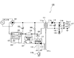
図1は、本実施形態に係る電源装置の関連技術の構成の一例を示す概略構成図である。
図1に示す電源装置であるAC/DC電源100は、交流電源(商用電源)から入力された交流電圧を直流電圧に変換して出力する。以下、AC/DC電源100の基本的な動作原理を説明する。
[First related technology ]
FIG. 1 is a schematic configuration diagram showing an example of the configuration of the related technology of the power supply device according to the present embodiment.
The AC /
AC/DC電源100に入力された交流電流は、整流器の一例であるダイオードブリッジ101によって整流され、その整流電流は平滑コンデンサ102に充電される。これにより平滑コンデンサ102の両端に直流電圧が得られる。この直流電圧は起動抵抗108を介してコンバータ制御回路110に電力を供給する。
コンバータ制御回路110は、平滑コンデンサ102とトランス111の間に直列に接続されたスイッチング素子109のスイッチング信号の出力を開始する。このスイッチングによって平滑コンデンサ102の後段に配置されたトランス111の1次巻き線111aに交流電流が流れる。
The alternating current input to the AC /
The
そして、この交流電流によってトランスの巻き線比に応じた電圧が2次側巻き線111bに発生する。2次側には2次側整流ダイオード114と2次側平滑コンデンサ115が配置されており、電圧が2次側整流ダイオード114で整流、2次側平滑コンデンサ115で平滑化される。そのため、2次側平滑コンデンサ115の両端に直流電圧が得られる。この2次側平滑コンデンサ115の両端から得られる電圧がAC/DC電源100の出力電圧Vout1となる。
Then, due to this alternating current, a voltage corresponding to the winding ratio of the transformer is generated in the secondary winding 111b. A secondary
また、出力電圧を一定の値に安定化させるために、抵抗136、137、シャントレギュレータ138、フォトカプラ116を介して、出力電圧Vout1をコンバータ制御回路110にフィードバックする。出力電圧Vout1は、抵抗136、137によって分圧され、シャントレギュレータ138に入力される。
Further, in order to stabilize the output voltage to a constant value, the output voltage Vout1 is fed back to the
シャントレギュレータ138は、抵抗分圧によって入力された電圧が基準電圧よりも高い場合は発光ダイオード116aに流す電流を増加させ、入力された電圧が基準電圧よりも低い場合は発光ダイオード116aに流す電流を減少させる。
発光ダイオード116aは、流れる電流の大きさに応じた光量で発光し、フォトトランジスタ116bを電気的に絶縁した状態でONさせる(発光ダイオード116aとフォトトランジスタ116bは同一のパッケージに入ったフォトカプラ116である)。フォトトランジスタ116bのコレクタには、受光した光量に応じた電流が流れる。
The
The
このようにして、AC/DC電源100の出力電圧がフォトカプラ116を介してコンバータ制御回路110にフィードバックされる。また、コンバータ制御回路110は、AC/DC電源100の出力電圧が一定の値に調製されるようにスイッチング素子109のデューティー比を制御する。
例えば、AC/DC電源100の出力電圧が低下した場合、より多くの電力を2次側に供給する必要があることからスイッチングのON時間を長くし、トランスの1次巻き線111aに流れる電流を大きくする。
また、トランスの1次巻き線111a、2次巻き線111bと同一のコアに補助巻き線111cが巻かれており、スイッチング素子109のスイッチングが開始されると同時に補助巻き線111cにも電圧が発生する。この電圧によってダイオード112に電流が流れてコンデンサ113を充電するため、コンデンサ113の両端に直流電圧が得られる。
コンデンサ113の電圧はコンバータ制御回路110の電力供給源となる。コンデンサ113の両端の直流電圧が電力供給源として供給されると、コンバータ制御回路110は、平滑コンデンサ102から起動抵抗108を介して供給されていた電力が遮断されるようにコンバータ制御回路110内の動作を制御する。次に、突入電流防止回路300の動作の一例について説明する。
In this way, the output voltage of the AC /
For example, when the output voltage of the AC /
Further, the auxiliary winding 111c is wound around the same core as the primary winding 111a and the secondary winding 111b of the transformer, and a voltage is generated in the auxiliary winding 111c at the same time when the switching of the
The voltage of the
AC/DC電源100は、突入電流防止回路300が有するリレー104のON(導通状態)/OFF(遮断状態)を制御する電流検知回路106を有する。
また、突入電流防止回路300のリレー104をONするタイミングは、AC/DC電源100の入力電流に応じて決定される。この入力電流を検知するために、AC/DC電源100は電流検知手段として機能する電流検知抵抗105を有する。電流検知回路106は突入電流防止抵抗103の動作を有効にするか否か(電流を流すか否か)を制御する制御手段として機能する。
なお、この入力電流は、AC/DC電源100の出力電力に依存しており、AC/DC電源100の出力電力が大きいほど入力電流も大きくなる。また、AC/DC電源100の出力電力が小さいほど入力電流も小さくなる。そのため、AC/DC電源100からの出力電力を基準にしてリレー104のON/OFFを制御してもよい。
The AC /
Further, the timing at which the
The input current depends on the output power of the AC /
図1に示すAC/DC電源100では、当該AC/DC電源100の1次側にコンバータのスイッチング電流を検知する電流検知抵抗105を配置しており、その両端電圧から入力電流の変化を検知する。
なお、第1の関連技術では、電流検知抵抗105で検知する電流値が第1電流値未満(第1の閾値未満)である場合には突入電流防止回路300の機能を有効とするようリレー104はOFFのままとする。また、電流値が第1電流値以上(第1の閾値以上)である場合には突入電流防止回路300の機能を無効とするようリレー104をONするように制御するものとする。
In the AC /
In the first related technique , when the current value detected by the
図2は、第1電流値(第1の閾値)の決定手順の一例を説明するためのグラフである。図2に示すグラフは、縦軸を突入電流防止回路300の電力損失とし、横軸をAC/DC電源100への入力電流としている。
FIG. 2 is a graph for explaining an example of a procedure for determining a first current value (first threshold value). In the graph shown in FIG. 2, the vertical axis represents the power loss of the inrush
ここで、例えば突入電流防止回路300のリレー104の状態が「OFF」であるとする。突入電流防止回路300のリレー104がOFFの場合、AC/DC電源100への入力電流は、コンデンサへの突入電流を制限する電流制限手段として機能する突入電流防止抵抗103を流れる。そのため、突入電流防止回路300の消費電力は入力電流の2乗に比例することになる。この場合、図2の実線で示すように突入電流防止回路300で生じる電力損失はAC/DC電源100の入力電流に応じて変動することになる。
Here, for example, it is assumed that the state of the
次に、突入電流防止回路300のリレー104の状態が「ON」であるとする。この場合、突入電流防止抵抗103がリレー104により短絡されているため電流が突入電流防止抵抗103を流れることによる電力損失は発生しない。しかしながら、リレー104をONするために約0.5[W]の電力が必要である。なお、この電力は図2の破線で示すようにAC/DC電源100の入力電流に依らず一定である。
Next, it is assumed that the state of the
以上のことから、図2に示すグラフのように、AC/DC電源100の入力電流がある一定の値(I0)を超えるまでは突入電流防止回路300のリレー104をOFFした方が低消費電力化を図ることができる。また、入力電流がI0を超えた後は突入電流防止回路300のリレー104をONした方が低消費電力化を図ることができる。
このI0を第1電流値(第1の閾値)として設定し、電流検知抵抗105で検知する電流が第1電流値(I0)を超えたときに突入電流防止回路300のリレー104をONする。
このようにAC/DC電源100の動作を制御することで突入電流防止回路300での電力損失を最も低減することができる。以下、I0の値の決定手順の一例について説明する。
From the above, as shown in the graph shown in FIG. 2, it is better to turn off the
This I0 is set as the first current value (first threshold value), and when the current detected by the
By controlling the operation of the AC /
突入電流防止回路300のリレー104の状態が「OFF」であるとき、つまり入力電流が突入電流防止抵抗103を流れるときのAC/DC電源100への入力電流をIinとする。このとき、突入電流防止回路300の消費電力は、突入電流防止抵抗103をR[Ω]とした場合、消費電力=Iin2×Rとして表すことができる。
この消費電力と、突入電流防止回路300のリレー104の状態が「ON」であるときの消費電力0.5[W]とが等しくなる場合の入力電流IinがI0になる。よって、I0は、突入電流防止抵抗103を10[Ω]としたとき下記の式(1)で表すことができる。
When the state of the
When this power consumption becomes equal to the power consumption of 0.5 [W] when the state of the

このときのAC/DC電源100への入力電力Pinは、入力電圧を100[V]としたとき下記の式(2)で表すことができる。
The input power Pin to the AC /
また、出力電力Poutは、AC/DC電源100の効率を85[%]としたとき下記の式(3)で表すことができる。
Further, the output power Pout can be expressed by the following equation (3) when the efficiency of the AC /
以上の計算に基づいて、第1電流値を0.22[A]とし、電流検知抵抗105で検知する電流が第1電流値を超えたときに突入電流防止回路300のリレー104をONすると、突入電流防止回路300での電力損失を最も低減することができる。
具体的には、I0 = 0.22[A]である場合は、AC/DC電源100の出力電力が18.7[W]を超えたときに突入電流防止回路300のリレー104をONするように制御する。
なお、第1電流値をI0に限定するものではなく、例えば突入電流防止抵抗103の定格電流や発熱が問題になるのであれば、第1電流値をI0より小さい値に設定してもよい。
Based on the above calculation, the first current value is set to 0.22 [A], and when the current detected by the
Specifically, when I0 = 0.22 [A], the
The first current value is not limited to I0. For example, if the rated current or heat generation of the inrush
次に、突入電流防止回路300のリレー104の状態が「ON」であり、AC/DC電源100への入力電流が減少(出力電力が低下)したとする。
この場合、電流検知抵抗105により検知される電流が第2電流値以下(第2の閾値以下)になったときに突入電流防止回路300のリレー104をOFFし、入力電流が再び突入電流防止抵抗103を通るように制御する。
このように制御する理由は、AC/DC電源100の入力電流が第2の電流値よりも小さくなるとリレー104をONし続けることによって生じる電力損失よりも、入力電流が突入電流防止抵抗103を流れることによる電力損失の方が小さいためである。
この第2電流値(第2の閾値)は、電流検知抵抗105で検知する電流の変動に対して突入電流防止回路300のリレー104のON/OFFが頻繁に切り替わらないようにするために第1電流値より小さい値を設定する。具体的には、例えばスイッチ107のON/OFFにヒステリシス特性を持たせる。
Next, it is assumed that the state of the
In this case, when the current detected by the
The reason for this control is that when the input current of the AC /
This second current value (second threshold value) is set to the first so that the ON / OFF of the
このように、第1の関連技術に係るAC/DC電源100は、従来では平滑コンデンサ102充電後はONし続けていた突入電流防止回路300のリレー104を、AC/DC電源100への入力電流(AC/DC電源100の出力電力)に応じて切り替える。これにより、突入電流防止回路300で生じる電力損失を低減することができる。
As described above, in the AC /
なお、第1の関連技術では、電流検知抵抗105を平滑コンデンサ102とスイッチング素子109の間に直列に接続し、コンバータのスイッチング電流からAC/DC電源100への入力電流の変化を検知しているが、このような構成に限定するものではない。
例えば、入力電流(突入電流防止抵抗103を流れる電流)に応じて変化するパラメータを検知できる構成であれば電流検知抵抗105の配置場所は問わない。
また、商用電源とダイオードブリッジ101の間に直列に接続してもよいし、AC/DC電源100の2次側に配置し出力電流を検知してもよい。また、突入電流防止回路300のスイッチ104としてリレーを記載しているがトライアック等の半導体素子(半導体スイッチ)を用いてもよい。
In the first related technique , a
For example, the location of the
Further, it may be connected in series between the commercial power supply and the
[第2の関連技術]
ここでは、AC/DC電源400を実装した画像形成装置を例に挙げて説明する。
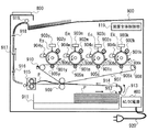
図3は、AC/DC電源400を有する画像形成装置の構成の一例を示す概略縦断面図である。
なお、画像形成装置900は、電子写真プロセスにより紙等の記録材Pに画像を形成する。
[Second related technology ]
Here, an image forming apparatus that implements an AC /
FIG. 3 is a schematic vertical sectional view showing an example of the configuration of an image forming apparatus having an AC /
The
画像形成装置900は、イエロー、マゼンタ、シアン、ブラックの4色のトナーを用いてフルカラーの画像を記録材Pに形成する。なお、図3に示す各種構成において符号の末尾に付されたy、m、c、kは、それぞれイエロー、マゼンタ、シアン、ブラックの画像形成部を示している。以下、4色の作像プロセスは同一であるためy、m、c、kの符号は省略して説明を進める。
The
画像形成装置900を動作させるためのユーザーからの指示は、ネットワークや操作部800を介して、当該画像形成装置900全体の動作を制御する装置全体制御部119へ送られる。以下説明する画像形成に伴う各負荷の動作は装置全体制御部119からの信号に基づいて制御される。
An instruction from the user for operating the
装置全体制御部119は、ユーザーからプリント開始の指示を受け付けた場合、感光体ドラム901、現像器904、中間転写ベルト駆動ローラ908、定着ローラ915がそれぞれ所定のスピードで回転するように駆動制御する。
感光体ドラム901は、図3に示す矢印の方向に向けて回転しており、その回転過程においてドラムの表面上にトナー像が形成される。
トナー像の形成は、帯電ローラ902によって感光体ドラム901表面の電位が一様になるように帯電され、プリントする画像データに基づいて変調されたレーザー光Eを感光体ドラム901に照射して感光体ドラム901の表面に潜像を形成する。その後、高電圧が印加された現像器904によって感光体ドラム901表面上の潜像をトナーによって現像する。
When the user gives an instruction to start printing, the overall
The photoconductor drum 901 is rotated in the direction of the arrow shown in FIG. 3, and a toner image is formed on the surface of the drum in the rotation process.
To form the toner image, the photoconductor drum 901 is charged with a charging roller 902 so that the potential on the surface of the photoconductor drum 901 becomes uniform, and the photoconductor drum 901 is irradiated with laser light E modulated based on the image data to be printed. A latent image is formed on the surface of the body drum 901. Then, the latent image on the surface of the photoconductor drum 901 is developed with toner by the developer 904 to which a high voltage is applied.
感光体ドラム901上に形成されたトナー像は、1次転写ローラ905によって中間転写ベルト907に転写される。転写後、中間転写ベルト907に転写されずに感光体ドラム901に残留したトナーは、感光体ドラムクリーナー906で掻きとられ、再び帯電ローラ902による帯電から作像プロセスが再開される。以上の処理を4色のトナーそれぞれにおいて同様に行うことで、中間転写ベルト907上にフルカラーのトナー像を形成する。
The toner image formed on the photoconductor drum 901 is transferred to the
また、記録材Pは、装置全体制御部119にプリントの指示が送られてから所定のタイミングで給紙カセット911から給紙される。
記録材Pの給紙は、ピックアップローラ912で記録材Pを給紙ローラ913に搬送する。給紙ローラ913では、記録材Pに対して上側のローラで紙の搬送方向に、下側のローラでピックアップローラ912の方向に向けて力を加えることで記録材Pが複数枚重なって搬送されることを防止する。
レジローラ914では、記録材Pの斜行防止のため記録材Pを湾曲させた状態で停止させておき、中間転写ベルト907上のトナー像が2次転写ローラ909を通過するタイミングで記録材Pの再搬送を行う。
Further, the recording material P is fed from the
To feed the recording material P, the
In the
また、2次転写ローラ909には高電圧が印加されており、中間転写ベルト907上のトナー像と記録材Pが同時に2次転写ローラ909を通過することでトナー像が記録材Pに転写される。転写後、記録材Pに転写されずに中間転写ベルト907に残留したトナーは、以降の作像に影響を及ぼさないようにするため、中間転写ベルトクリーナー910によって掻きとられる。記録材Pに転写されたトナー像は定着ローラ915によって熱と圧力が加えられ、当該トナー像が記録材Pに定着される。
Further, a high voltage is applied to the
そして、画像が形成された記録材Pは、搬送ローラ916、917、918、919を介して画像形成装置900の外部に排紙される。
このように、画像形成装置900はその動作を達成するためには演算装置、センサ、モータ、高圧電源等への電力の供給が必要である。その電力供給源として商用電源から入力された交流電圧を直流電圧に変換して出力するAC/DC電源100を備えている。
Then, the recording material P on which the image is formed is discharged to the outside of the
As described above, in order to achieve the operation of the
ここで、画像形成装置は、その動作状況に応じて様々な動作モードを有している。例えば、各種の動作モードを大きく分けるとスリープモード、スタンバイモード、プリントモードの3つがある。
画像形成装置900は、上記したスリープモード、スタンバイモード、プリントモードの3つの動作モードを有するものとして説明を進める。
Here, the image forming apparatus has various operation modes depending on its operation state. For example, various operation modes can be roughly divided into three modes: sleep mode, standby mode, and print mode.
スリープモードは、画像形成装置900が最も小さい消費電力(例えば5[W]以下)で動作するモードであり、プリントの指示を受けるための演算回路のみ動作させ、それ以外の負荷は動作を停止させている。そのため、プリントの指示を受けてからプリントを開始できるまでに比較的長い時間を要する。
スタンバイモードは、画像形成装置900がプリントの指示を受けたときに最短時間でプリントを開始できる状態であり、スリープモードよりも消費電力は大きい(例えば100[W]〜200[W])。しかしながら、プリントの指示を受けてからプリントを開始できるまでを高速化することができる。
プリントモードは、記録材Pに画像形成を行っている状態であり、画像形成を行うために必要な全ての負荷に電力を供給している。よって消費電力は最も大きい(例えば1500[W])。
なお、これら各動作モードはユーザーからの指示や時間経過(待機時間)によって切り替わるものとする。
The sleep mode is a mode in which the
The standby mode is a state in which printing can be started in the shortest time when the
The print mode is a state in which an image is formed on the recording material P, and power is supplied to all the loads necessary for performing the image formation. Therefore, the power consumption is the largest (for example, 1500 [W]).
It should be noted that each of these operation modes is switched according to an instruction from the user or the passage of time (standby time).
図4は、画像形成装置900が有するAC/DC電源400の機能構成の一例を示す図である。
画像形成装置900が有するAC/DC電源400は、当該画像形成装置900がコンセントに接続している間は常に動作している待機時電源200を有する。AC/DC電源400は、また、画像形成装置900が消費電力の大きいモードに切り替わったときのみ動作させる大電力電源201を有する。待機時電源200は、CPU等の演算回路から成る装置全体制御部119に電力を供給する。また、大電力電源201は高圧基板やモータ等、電力仕様の大きい負荷146に電力を供給する。
FIG. 4 is a diagram showing an example of the functional configuration of the AC /
The AC /
大電力電源201は、画像形成装置900の動作モードがスリープモード中であるとき、低消費電力化のために動作を停止するように制御される。また、画像形成装置900の動作モードがスタンバイモードやプリントモードに切り替わったとき動作を開始するように制御される。装置全体制御部119は、操作部800やネットワークを介したユーザーからの指示に基づいて、大電力電源201の動作や画像形成装置900が有する各負荷(負荷146等)の動作を制御するための信号(制御信号)を出力する。
The high
図5は、待機時電源200の機能構成の一例を示す図である。
なお、第1の関連技術において説明したAC/DC電源100の機能構成と同じものは同一の符号を付すとともにその説明を省略する。
FIG. 5 is a diagram showing an example of the functional configuration of the
Those having the same functional configuration as the AC /
AC/DC電源400(待機時電源200)は、突入電流によってダイオードブリッジ101等が破壊されることを防ぐために突入電流防止回路300を有する。
なお、画像形成装置900では、画像形成装置の動作モードに応じて突入電流防止回路300のリレー104のON/OFFを切り替える。
The AC / DC power supply 400 (standby power supply 200) has an inrush
In the
装置全体制御部119は、リレー104のON/OFFを切り替えるスイッチ107の動作を制御する。具体的には、装置全体制御部119がフォトカプラ118を介して、画像形成装置900の動作モードに基づいた信号をスイッチ107に向けて出力する。
なお、画像形成装置900の動作モードと突入電流防止回路300のリレー104のON/OFFの制御は図6に示す対応表に従うものとする。
The overall
The operation mode of the
図6は、画像形成装置900の動作モードと突入電流防止回路300のリレー104の状態(ON又はOFF)を関連付けた表である。
画像形成装置900の動作モードがスリープモード(第1の動作モード)である場合、装置全体制御部119は、突入電流防止回路300のリレー104をOFFにする信号を出力する。
画像形成装置900の動作モードが第1の動作モードである場合、AC/DC電源400への入力電流が小さい(例えば数十mA)。そのため、突入電流防止回路300のリレー104をONし続けるよりも、入力電流が突入電流防止抵抗103を通ることによる電力損失の方が小さい。つまり、第1の動作モードのときには突入電流防止回路300のリレー104をOFFし、入力電流を突入電流防止抵抗103に流し続けた方が低消費電力化を図ることができる。
FIG. 6 is a table associating the operation mode of the
When the operation mode of the
When the operation mode of the
また、画像形成装置900の動作モードがスタンバイモードやプリントモード(第2の動作モード)に切り替わったときは、装置全体制御部119は、突入電流防止回路300のリレー104をONにする信号を出力する。
画像形成装置900の動作モードが第2の動作モードである場合、AC/DC電源100の出力電力が大きいため、入力電流も大きくなる(例えば数A〜十数A)。そのため、入力電流が突入電流防止抵抗103に流れ続けてしまうと電力損失が大きくなる。
つまり、第2の動作モードのときにはリレー104をONし、突入電流防止抵抗103を短絡することで低消費電力化を図ることができる。
When the operation mode of the
When the operation mode of the
That is, in the second operation mode, the
また、画像形成装置900の動作モードが再びスリープモードになった場合、装置全体制御部119は、突入電流防止回路300のリレー104をOFFにする信号を出力する。
このように、画像形成装置900の動作モードに応じて装置全体制御部119は、スイッチ107に対して突入電流防止回路300のリレー104のON/OFFを制御する信号を出力する。
以下、突入電流防止回路300のリレー104の状態をON又はOFFする制御の処理手順について説明する。
Further, when the operation mode of the
In this way, the overall
Hereinafter, the processing procedure of the control for turning on or off the state of the
図7は、画像形成装置900の動作を制御する処理手順の一例を示すフローチャートである。
なお、図7では、画像形成装置900がスリープモードの状態でプリントの指示を受けてプリントモードに移行し、画像形成を行いその後再びスリープモードに戻るまでの処理手順を示している。また、図7に示す各処理は、主として装置全体制御部119により実行される。また、初期状態として画像形成装置900の動作モードがスリープモードのときは、リレー104の状態はOFFになっている。
FIG. 7 is a flowchart showing an example of a processing procedure for controlling the operation of the
Note that FIG. 7 shows a processing procedure in which the
装置全体制御部119は、ユーザーからプリントの指示を受け付けたか否かを判別する(S602)。プリントの指示を受けていないと判別した場合(S602:No)、スリープモードを維持する。また、そうでない場合(S602:Yes)、装置全体制御部119は、リレー104をONし(S603)、画像形成装置900の動作モードをプリントモードへ移行する(S604)。
The overall
装置全体制御部119は、ユーザーから指示されたジョブが完了したか否かを判別する(S605)。完了していないと判別した場合(S605:Yes)、プリントモードを維持する。なお、その間はリレー104の状態はONのままである。
The overall
装置全体制御部119は、ユーザーから指示されたジョブが完了したと判別した場合(S605:No)、画像形成装置900の動作モードをスタンバイモードへ移行する(S606)。なお、画像形成装置900がスタンバイモードで動作している間もリレー104はONのままである。
When the entire
装置全体制御部119は、ユーザーから画像形成装置900の動作モードをスリープモードへ移行させる指示を受け付けたか否かを判別する(S607)。移行指示を受け付けた場合(S607:Yes)、装置全体制御部119は、リレー104をOFFし(S609)、画像形成装置900の動作モードをスリープモードへ移行する。この場合、画像形成装置900は初期状態に戻ることになる。
The device-
装置全体制御部119は、移行指示を受け付けていない場合(S607:No)、スタンバイモードに移行してから一定時間が経過したか否かを判別する(S608)。つまり、スタンバイモードに移行してから一定時間が経過したときには自動的にスリープモードに移行することになる。
When the shift instruction is not received (S607: No), the overall
装置全体制御部119は、一定時間が経過していないと判別した場合(S608:No)、ユーザーから画像形成装置900の動作モードをスリープモードへ移行させる指示を受け付けたか否かを判別する(S611)。移行指示を受け付けた場合(S611:Yes)、ステップS604の処理に戻る。この場合、画像形成装置900は再び指示されたジョブを完了するまでプリントモードで動作することになる。また、そうでない場合(S611:No)、ステップS607の処理に戻る。この場合、画像形成装置900は再びスリープモードになるまでスタンバイモードで動作することになる。
When it is determined that the fixed time has not elapsed (S608: No), the overall
装置全体制御部119は、一定時間が経過したと判別した場合(S608:Yes)、リレー104をOFFし(S609)、画像形成装置900の動作モードをスリープモードへ移行する。
このように、リレー104は画像形成装置900の動作モードがスリープモードのときにはOFFされ、スタンバイモードとプリントモードのときにはONされるように制御される。
When the device-
In this way, the
このように、画像形成装置900は、従来では平滑コンデンサ102充電後はONし続けていた突入電流防止回路300のリレー104の状態を装置の動作モードに応じて切り替える。これにより、突入電流防止回路300で生じる電力損失を低減することができる。
In this way, the
なお、第2の関連技術では、突入電流防止回路300のリレー104をスリープモードではOFFし、スタンバイモードとプリントモードではONするとしたが、装置の動作モードとリレー104のON/OFFの関係はこれに限るものではない。
例えば、スタンバイモード時のAC/DC電源の入力電流が小さい場合(一例として、第1実施形態において示した0.22[A]以下、出力電力に換算すると18.7[W]以下の場合)は、スタンバイモードであってもリレー104をOFFしてもよい。
In the second related technology , the
For example, when the input current of the AC / DC power supply in the standby mode is small (for example, when it is 0.22 [A] or less shown in the first embodiment, and when converted to output power, it is 18.7 [W] or less). May turn off the
[実施形態]
ここでは、第2の関連技術のAC/DC電源400(待機時電源200)とは異なる待機時電源について説明する。なお、第1、第2の関連技術において説明したAC/DC電源の機能構成と同じものは同一の符号を付すとともにその説明を省略する。
[Implementation form]
Here, a standby power supply different from the AC / DC power supply 400 (standby power supply 200) of the second related technology will be described. Those having the same functional configuration as the AC / DC power supply described in the first and second related techniques are designated by the same reference numerals, and the description thereof will be omitted.
図8は、本実施形態に係る待機時電源の機能構成の一例を示す図である。
図4に示す待機時電源200の構成と異なる部分は、図8に示す待機時電源ではコンバータ部の前段にPFC回路(力率改善回路)301を有している点である。
PFC回路301は、コイル121、ダイオード122、スイッチング素子123を含んで構成される昇圧回路であり、入力電流の大きいAC/DC電源の力率改善や高調波対策に用いられる回路である。
FIG. 8 is a diagram showing an example of the functional configuration of the standby power supply according to the present embodiment.
The difference from the configuration of the
The
PFC回路301では、出力電圧を一定の値に安定させるためにPFC回路301の出力電圧を電圧検知抵抗139、140で分圧し、PFC制御回路124にフィードバックする。
PFC制御回路124は、フィードバックされた電圧と基準電圧とを比較する。また、PFC制御回路124は、ダイオード141、142、抵抗143、144により入力電圧波形を検知する。PFC制御回路124は、フィードバックされた電圧と基準電圧と偏差を減らすように、且つ、入力電流波形が入力電圧と相似の正弦波になるようにスイッチング素子123のデューティー比を制御する。
なお、通常であればPFC回路は大電力用のAC/DC電源に用いられるものであり、低電力の待機時電源には用いる必要がない。しかしながら、待機時電源を大電力化する際は入力電流が大きくなるため、力率改善や高調波対策として待機時電源であってもPFC回路を用いる必要が生じる。
In the
The
Normally, the PFC circuit is used for a high-power AC / DC power supply, and does not need to be used for a low-power standby power supply. However, since the input current becomes large when the standby power supply is increased in power, it is necessary to use the PFC circuit even in the standby power supply as a power factor improvement or a measure against harmonics.
また、PFC回路301を用いる場合に問題となるのが、装置の動作モードがスリープモードであるときの消費電力である。PFC回路301は、スイッチング素子123のスイッチングにより昇圧をする回路であるため、そのスイッチング動作やPFC制御回路124、電圧検知抵抗139、140、143、144により電力を消費する。
一方、待機時電源はスリープモード中においても動作をしているAC/DC電源である。近年、画像形成装置には省エネ対応が要求されていることから、待機時電源の電力損失の増加によってスリープモード時における消費電力の増加は望ましくない。
Further, when the
On the other hand, the standby power supply is an AC / DC power supply that operates even in the sleep mode. In recent years, since the image forming apparatus is required to support energy saving, it is not desirable to increase the power consumption in the sleep mode due to the increase in the power loss of the standby power supply.
そこで、本実施形態に係る待機時電源のように、画像形成装置900の動作モードがスリープモードであれば当該待機時電源のPFC回路301の動作を停止させる。これにより、スイッチング素子123やPFC制御回路124、電圧検知抵抗139、140、143、144で生じる電力損失を低減させることができる。
Therefore, if the operation mode of the
また、PFC回路301はAC/DC電源への入力電流が大きい場合は動作をさせる必要があるが、入力電流が小さく、力率や高調波が問題とならない場合は動作をさせる必要がない。よって、スリープモードのようなAC/DC電源への入力電流が小さい動作モードにおいては、PFC回路301の動作を停止させておくことができる。
一方、画像形成装置900が消費電力の大きい動作モードに切り替わったときは、PFC回路301を動作させて高調波対策や力率改善を図ることになる。
Further, the
On the other hand, when the
装置全体制御部119は、PFC回路301を動作させる、又は動作を停止させることを制御する。装置全体制御部119は、画像形成装置900の動作モードに基づいて、フォトカプラ118を介して、PFC回路301のON/OFF信号をPFC制御回路124に向けて出力する。
なお、本実施形態では、待機時電源における突入電流防止回路300のリレー104のON/OFFの制御を、PFC回路301のON/OFFを制御する信号と同一の信号、つまり1つの信号でリレー104とPFC回路301の動作を制御するものとする。また、画像形成装置900の動作モードとPFC回路301のON/OFF、突入電流防止回路300のリレー104のON/OFFは、図9に示す対応表に従うものとする。
The entire
In the present embodiment, the ON / OFF control of the
図9は、画像形成装置900の動作モードとPFC回路301の動作(ON/OFF)、リレー104の動作(ON/OFF)を関連付けた表である。
図10は、図9に示す対応表に基づくPFC回路301の動作(ON/OFF)、リレー104の動作(ON/OFF)を説明するための図である。
以下、図9、図10を用いてPFC回路301の動作(ON/OFF)、リレー104の動作(ON/OFF)を説明する。
FIG. 9 is a table associating the operation mode of the
FIG. 10 is a diagram for explaining the operation (ON / OFF) of the
Hereinafter, the operation (ON / OFF) of the
待機時電源200の出力電力が大きい場合、入力電流が大きくなるのでPFC回路301を動作させる必要がある。しかし、待機時電源200の出力電力が小さい(P1以下)場合は入力電流が小さくなるためPFC回路301を動作させる必要はない。
この場合、待機時電源200の出力電力がP1以下ならば、低消費電力化のためPFC回路301を停止させておくことが望ましい。
When the output power of the
In this case, if the output power of the
突入電流防止回路300のリレー104では、待機時電源200の出力電力が大きい場合は入力電流が大きくなるためリレーをONし、入力電流が突入電流防止抵抗103を流れることで発生する電力の損失を防ぐ。しかし、待機時電源200の出力電力が小さい(P2以下)場合は入力電流が小さくなるためリレー104をONするために必要な電力よりも、入力電流が突入電流防止抵抗103を流れることで消費する電力の方が小さい。
そのため、待機時電源200の出力電力がP2以下ならば、低消費電力化のためリレー104をOFFにすることが望ましい(P2の値は、例えば第1の関連技術の計算例によると18.7[W])。
なお、P1とP2それぞれの値は必ずしも一致しない。これは待機時電源の「PFC回路301のON/OFFを切り替えるべき出力電力」と「突入電流防止回路300のリレー104のON/OFFを切り替えるべき出力電力」が異なることを意味する。
In the
Therefore, if the output power of the
The values of P1 and P2 do not always match. This means that the "output power for switching ON / OFF of the
また、待機時電源200の出力電力は連続的にあらゆる値をとるわけではなく、画像形成装置の動作モードに応じてある程度一定の値になる。
ここで、スリープモード、スタンバイモード、プリントモードの待機時電源の出力電力をそれぞれPsleep、Pstandby、Pprintとし、出力電力の大小関係はPsleep<Pstandby<Pprintであるとする。また、P1、P2、Psleep、Pstandby、Pprintそれぞれの値の大小関係が図10の横軸に示す関係にあるとする。
Further, the output power of the
Here, it is assumed that the output powers of the standby power supplies in the sleep mode, the standby mode, and the print mode are Psleep, Pstandby, and Print, respectively, and the magnitude relation of the output powers is Psleep <Pstandby <Print. Further, it is assumed that the magnitude relationship between the values of P1, P2, Psleep, Pstandby, and Pprint is the relationship shown on the horizontal axis of FIG.
この場合、スリープモードのときは、PFC回路301と突入電流防止回路300のリレー104を両方ともOFFにすることが望ましい。また、スタンバイモードとプリントモードのときはPFC回路301と突入電流防止回路300のリレー104を両方ともONにすることが望ましいことが見て取れる。つまり、P1とP2の値は異なるものの、画像形成装置の各動作モードにおけるPFC回路301と突入電流防止回路300のリレー104のON/OFFの関係は一致している。
そのため、PFC回路301のON/OFFと突入電流防止回路300のリレー104のON/OFFを別々の信号で制御する必要がなくなる。つまり、装置全体制御部119から出力する1つの信号によりPFC回路301と突入電流防止回路300のリレー104の両方を同時に制御することが可能になる。
In this case, it is desirable to turn off both the
Therefore, it is not necessary to control the ON / OFF of the
このように、本実施形態に係る画像形成装置900は、PFC回路301のON/OFFと突入電流防止回路300のリレー104のON/OFFを1つの信号により制御し、画像形成装置の動作モードに応じて切り替える。これにより、突入電流防止回路300で生じる電力損失を低減することができる。
また、待機時電源200にPFC回路301を用いる場合に、PFC回路301のON/OFFの切り替えと、突入電流防止回路300のリレー104のON/OFFの切り替えを同一の信号で行うことができる。そのため、別々の信号で制御する場合と比べて回路の小型化、低コスト化を図ることが可能になる。
As described above, the
Further, when the
なお、画像形成装置900の動作モードとPFC回路301のON/OFF、突入電流防止回路300のリレー104のON/OFFの関係は図9の対応表に限るものではない。
例えば、図10において、PstandbyがP1とP2の両方より小さければスタンバイモードでもPFC回路301と突入電流防止回路300のリレー104はOFFにしてもよい。
The relationship between the operation mode of the
For example, in FIG. 10, if the Pstandby is smaller than both P1 and P2, the
上記説明した実施形態は、本発明をより具体的に説明するためのものであり、本発明の範囲が、これらの例に限定されるものではない。 The embodiments described above are for more specific description of the present invention, and the scope of the present invention is not limited to these examples.
100・・・AC/DC電源(電源装置)、101・・・ダイオードブリッジ(整流回路)、102・・・平滑コンデンサ、103・・・突入電流防止抵抗、104・・・スイッチ(突入電流防止抵抗短絡用)、105・・・電流検知抵抗、106・・・突入電流防止回路制御回路、107・・・トランジスタ(突入電流防止回路制御用)、108・・・起動抵抗、109・・・スイッチング素子(コンバータ用)、110・・・コンバータ制御回路、119・・・装置全体制御部、200・・・待機時電源、201・・・大電力電源、300・・・突入電流防止回路、301・・・PFC回路、800・・・操作部、900・・・画像形成装置。 100 ... AC / DC power supply (power supply device), 101 ... diode bridge (rectifier circuit), 102 ... smoothing capacitor, 103 ... inrush current prevention resistance, 104 ... switch (rush current prevention resistance) (For short circuit), 105 ... Current detection resistance, 106 ... Inrush current prevention circuit control circuit, 107 ... Transistor (for inrush current prevention circuit control), 108 ... Start resistance, 109 ... Switching element (For converter), 110 ... Converter control circuit, 119 ... Device overall control unit, 200 ... Standby power supply, 201 ... High power power supply, 300 ... Inrush current prevention circuit, 301 ... -PFC circuit, 800 ... operation unit, 900 ... image forming device.
Claims (5)
前記電源装置は、
前記入力された交流電圧を整流する整流器と、
前記整流された電圧を平滑するコンデンサと、
前記コンデンサが充電されるときに前記コンデンサに入力される電流を制限する電流制限手段と、
前記コンデンサの上段に設けられ、前記電源装置の力率を改善するための力率改善回路と、
前記コンデンサの後段に接続され、当該コンデンサにより平滑された電圧を所定の直流電圧に調製するコンバータと、
前記画像形成装置の電力モードに応じて前記力率改善回路を有効にするか否か及び前記電力モードに応じて前記電流制限手段を有効にするか否かを制御する制御手段と、を有し、
前記電源装置は前記第1電力モードと前記第2電力モードの両方で動作し、
前記制御手段は、前記電力モードが前記第1電力モードである場合は、前記力率改善回路を無効にし、前記電流制限手段を有効にするために、前記力率改善回路と前記電流制限手段に共通な制御信号を出力し、前記電力モードが前記第2電力モードである場合は、前記力率改善回路を有効にし、前記電流制限手段を無効にするために、前記力率改善回路と前記電流制限手段に共通な制御信号を出力することを特徴とする、
画像形成装置。 From the first power mode, which has a power supply device that converts the AC voltage input from the AC power supply into a DC voltage, cuts off the power supply to other than the specified load, and aims to reduce power consumption, and the first power mode. Is an image forming apparatus having a plurality of power modes including a second power mode having a large power consumption.
The power supply unit
A rectifier that rectifies the input AC voltage and
A capacitor that smoothes the rectified voltage and
A current limiting means that limits the current input to the capacitor when it is charged, and
A power factor improving circuit provided above the capacitor to improve the power factor of the power supply device,
A converter that is connected to the subsequent stage of the capacitor and adjusts the voltage smoothed by the capacitor to a predetermined DC voltage.
It has a control means for controlling whether or not the power factor improving circuit is enabled according to the power mode of the image forming apparatus and whether or not the current limiting means is enabled according to the power mode. ,
The power supply operates in both the first power mode and the second power mode.
When the power mode is the first power mode, the control means informs the power factor improving circuit and the current limiting means in order to disable the power factor improving circuit and enable the current limiting means. When a common control signal is output and the power mode is the second power mode, the power factor improving circuit and the current are used to enable the power factor improving circuit and disable the current limiting means. It is characterized by outputting a control signal common to the limiting means.
Image forming device.
前記制御手段は、前記画像形成装置の電力モードに応じて前記共通の制御信号により前記スイッチ手段の状態をON又はOFFにすることにより前記電流制限手段を有効にするか否かを決定することを特徴とする、
請求項1に記載の画像形成装置。 The power supply unit has a switch means connected in parallel with the current limiting means.
The control means determines whether or not to enable the current limiting means by turning the state of the switch means ON or OFF by the common control signal according to the power mode of the image forming apparatus. Characteristic,
The image forming apparatus according to claim 1.
前記制御手段は、前記画像形成装置の電力モードが前記第1電力モードである場合には前記昇圧手段の動作を停止させ、前記スイッチ手段の状態をOFFにすることにより前記電流制限手段を有効にすることを特徴とする、
請求項2に記載の画像形成装置。 The power supply device has a boosting means capable of switching operation or stop of operation according to the power mode of the image forming device.
When the power mode of the image forming apparatus is the first power mode, the control means stops the operation of the boosting means and turns off the state of the switch means to effectively enable the current limiting means. Characterized by
The image forming apparatus according to claim 2.
請求項1ないし3のいずれか1項に記載の画像形成装置。 The current limiting means has a resistor connected in series with a power supply line through which a current rectified by the rectifier flows.
The image forming apparatus according to any one of claims 1 to 3.
請求項3に記載の画像形成装置。 The control means is characterized in that the operation of the boosting means is stopped based on the common control signal.
The image forming apparatus according to claim 3.
Priority Applications (2)
| Application Number | Priority Date | Filing Date | Title |
|---|---|---|---|
| JP2017115267A JP6949567B2 (en) | 2017-06-12 | 2017-06-12 | Image forming device |
| US16/002,043 US10971999B2 (en) | 2017-06-12 | 2018-06-07 | Power supply apparatus and image forming apparatus including a controller for controlling a current limiter |
Applications Claiming Priority (1)
| Application Number | Priority Date | Filing Date | Title |
|---|---|---|---|
| JP2017115267A JP6949567B2 (en) | 2017-06-12 | 2017-06-12 | Image forming device |
Publications (3)
| Publication Number | Publication Date |
|---|---|
| JP2019004541A JP2019004541A (en) | 2019-01-10 |
| JP2019004541A5 JP2019004541A5 (en) | 2021-03-25 |
| JP6949567B2 true JP6949567B2 (en) | 2021-10-13 |
Family
ID=64563817
Family Applications (1)
| Application Number | Title | Priority Date | Filing Date |
|---|---|---|---|
| JP2017115267A Active JP6949567B2 (en) | 2017-06-12 | 2017-06-12 | Image forming device |
Country Status (2)
| Country | Link |
|---|---|
| US (1) | US10971999B2 (en) |
| JP (1) | JP6949567B2 (en) |
Families Citing this family (7)
| Publication number | Priority date | Publication date | Assignee | Title |
|---|---|---|---|---|
| JP7254533B2 (en) * | 2019-01-18 | 2023-04-10 | キヤノン株式会社 | image forming device |
| US11239776B2 (en) * | 2019-02-11 | 2022-02-01 | Regal Beloit America, Inc. | Motor controller having low standby power consumption |
| JP7222278B2 (en) * | 2019-03-13 | 2023-02-15 | 株式会社リコー | image forming device |
| JP2021100297A (en) * | 2019-12-20 | 2021-07-01 | キヤノン株式会社 | Power supply device and system |
| CN111049394B (en) * | 2019-12-31 | 2021-05-18 | 联想(北京)有限公司 | Power supply circuit, circuit control method, power supply adapter, and electronic device |
| JP7421341B2 (en) | 2020-01-06 | 2024-01-24 | キヤノン株式会社 | Power supply and image forming device |
| JP7463886B2 (en) | 2020-07-03 | 2024-04-09 | 株式会社リコー | Power supply device, electronic device and image forming apparatus |
Family Cites Families (12)
| Publication number | Priority date | Publication date | Assignee | Title |
|---|---|---|---|---|
| JPH11212408A (en) | 1998-01-23 | 1999-08-06 | Ricoh Co Ltd | Image forming device |
| US6163712A (en) * | 1998-02-04 | 2000-12-19 | Motorola, Inc. | Inrush current limiter with output voltage detection for control of input current level and activation of current bypass path |
| JP4644959B2 (en) * | 2001-03-21 | 2011-03-09 | ソニー株式会社 | Power supply |
| TW539934B (en) * | 2001-12-06 | 2003-07-01 | Delta Electronics Inc | Inrush current suppression circuit |
| US20040174152A1 (en) * | 2003-03-04 | 2004-09-09 | Hwang Jeffrey H. | Pulse-skipping switching power converter |
| JP2005323453A (en) | 2004-05-10 | 2005-11-17 | Harison Toshiba Lighting Corp | Rush current preventive circuit |
| JP4577837B2 (en) * | 2005-04-26 | 2010-11-10 | ニチコン株式会社 | Switching power supply |
| KR101582090B1 (en) * | 2009-09-03 | 2016-01-04 | 삼성전자주식회사 | Apparatus and method for supplying power to image forming apparatus |
| US8422179B2 (en) * | 2009-07-22 | 2013-04-16 | Intersil Americas Inc. | Inrush current control |
| US8885308B2 (en) * | 2011-07-18 | 2014-11-11 | Crane Electronics, Inc. | Input control apparatus and method with inrush current, under and over voltage handling |
| US9302912B2 (en) * | 2012-03-28 | 2016-04-05 | Mks Instruments, Inc. | Compact, configurable power supply for energizing ozone-producing cells |
| JP5488647B2 (en) * | 2012-06-18 | 2014-05-14 | 株式会社リコー | Switching power supply device and image forming apparatus equipped with the same |
-
2017
- 2017-06-12 JP JP2017115267A patent/JP6949567B2/en active Active
-
2018
- 2018-06-07 US US16/002,043 patent/US10971999B2/en active Active
Also Published As
| Publication number | Publication date |
|---|---|
| JP2019004541A (en) | 2019-01-10 |
| US20180358889A1 (en) | 2018-12-13 |
| US10971999B2 (en) | 2021-04-06 |
Similar Documents
| Publication | Publication Date | Title |
|---|---|---|
| JP6949567B2 (en) | Image forming device | |
| JP2019004541A5 (en) | ||
| JP6218467B2 (en) | Power supply device and image forming apparatus | |
| JP5873293B2 (en) | Power supply device and image forming apparatus | |
| KR101248910B1 (en) | Switching mode power supply and image forming device having the same and method of driving thereof | |
| JP6308771B2 (en) | Image forming apparatus | |
| JP5515326B2 (en) | Power supply apparatus, image forming apparatus, and program | |
| US10148167B2 (en) | Power supply device and control method | |
| JP2015230451A (en) | Image forming apparatus | |
| EP2390996B1 (en) | Current resonance power supply | |
| JP5611568B2 (en) | Power supply circuit and image forming apparatus | |
| JP2012010434A (en) | Power supply device and image forming apparatus | |
| JP2014204643A (en) | Power supply and image formation device | |
| JP5540769B2 (en) | Power supply device and image forming apparatus | |
| JP6188371B2 (en) | Power supply device and image forming apparatus | |
| JP5939770B2 (en) | Image forming apparatus | |
| JP6885163B2 (en) | Power supply and image forming equipment | |
| JP2012120315A (en) | Switching power supply device and image forming device having the same | |
| JP7318528B2 (en) | Power supply circuit and electronic equipment with power supply circuit | |
| JP2018126037A (en) | Power supply device and electrical equipment | |
| JP6760087B2 (en) | Control method of power supply device, image forming device, and overcurrent protection circuit | |
| JP4994721B2 (en) | Image forming apparatus | |
| JP6635681B2 (en) | Image forming device | |
| JP2015050845A (en) | Power source device and image forming apparatus | |
| JP2014143834A (en) | Image forming apparatus and power source device |
Legal Events
| Date | Code | Title | Description |
|---|---|---|---|
| A621 | Written request for application examination |
Free format text: JAPANESE INTERMEDIATE CODE: A621 Effective date: 20200610 |
|
| A521 | Written amendment |
Free format text: JAPANESE INTERMEDIATE CODE: A523 Effective date: 20210208 |
|
| A977 | Report on retrieval |
Free format text: JAPANESE INTERMEDIATE CODE: A971007 Effective date: 20210322 |
|
| A131 | Notification of reasons for refusal |
Free format text: JAPANESE INTERMEDIATE CODE: A131 Effective date: 20210406 |
|
| A521 | Written amendment |
Free format text: JAPANESE INTERMEDIATE CODE: A523 Effective date: 20210603 |
|
| TRDD | Decision of grant or rejection written | ||
| A01 | Written decision to grant a patent or to grant a registration (utility model) |
Free format text: JAPANESE INTERMEDIATE CODE: A01 Effective date: 20210824 |
|
| A61 | First payment of annual fees (during grant procedure) |
Free format text: JAPANESE INTERMEDIATE CODE: A61 Effective date: 20210922 |
|
| R151 | Written notification of patent or utility model registration |
Ref document number: 6949567 Country of ref document: JP Free format text: JAPANESE INTERMEDIATE CODE: R151 |