JP6711185B2 - Power converter - Google Patents
Power converter Download PDFInfo
- Publication number
- JP6711185B2 JP6711185B2 JP2016138517A JP2016138517A JP6711185B2 JP 6711185 B2 JP6711185 B2 JP 6711185B2 JP 2016138517 A JP2016138517 A JP 2016138517A JP 2016138517 A JP2016138517 A JP 2016138517A JP 6711185 B2 JP6711185 B2 JP 6711185B2
- Authority
- JP
- Japan
- Prior art keywords
- capacitor
- voltage
- terminal
- phase
- inverter circuit
- Prior art date
- Legal status (The legal status is an assumption and is not a legal conclusion. Google has not performed a legal analysis and makes no representation as to the accuracy of the status listed.)
- Active
Links
- 239000003990 capacitor Substances 0.000 claims description 185
- 238000000034 method Methods 0.000 claims description 77
- 230000008569 process Effects 0.000 claims description 75
- 238000006243 chemical reaction Methods 0.000 claims description 40
- 230000007935 neutral effect Effects 0.000 claims description 19
- 238000010586 diagram Methods 0.000 description 10
- 230000008859 change Effects 0.000 description 9
- 230000004048 modification Effects 0.000 description 4
- 238000012986 modification Methods 0.000 description 4
- 230000002411 adverse Effects 0.000 description 3
- 238000010248 power generation Methods 0.000 description 3
- 230000002123 temporal effect Effects 0.000 description 3
- 230000007547 defect Effects 0.000 description 1
- 238000007599 discharging Methods 0.000 description 1
- 238000009499 grossing Methods 0.000 description 1
- 230000007257 malfunction Effects 0.000 description 1
- 238000004519 manufacturing process Methods 0.000 description 1
- 230000007704 transition Effects 0.000 description 1
Images


Classifications
-
- H—ELECTRICITY
- H02—GENERATION; CONVERSION OR DISTRIBUTION OF ELECTRIC POWER
- H02M—APPARATUS FOR CONVERSION BETWEEN AC AND AC, BETWEEN AC AND DC, OR BETWEEN DC AND DC, AND FOR USE WITH MAINS OR SIMILAR POWER SUPPLY SYSTEMS; CONVERSION OF DC OR AC INPUT POWER INTO SURGE OUTPUT POWER; CONTROL OR REGULATION THEREOF
- H02M7/00—Conversion of ac power input into dc power output; Conversion of dc power input into ac power output
- H02M7/42—Conversion of dc power input into ac power output without possibility of reversal
- H02M7/44—Conversion of dc power input into ac power output without possibility of reversal by static converters
- H02M7/48—Conversion of dc power input into ac power output without possibility of reversal by static converters using discharge tubes with control electrode or semiconductor devices with control electrode
- H02M7/483—Converters with outputs that each can have more than two voltages levels
- H02M7/487—Neutral point clamped inverters
-
- H—ELECTRICITY
- H02—GENERATION; CONVERSION OR DISTRIBUTION OF ELECTRIC POWER
- H02M—APPARATUS FOR CONVERSION BETWEEN AC AND AC, BETWEEN AC AND DC, OR BETWEEN DC AND DC, AND FOR USE WITH MAINS OR SIMILAR POWER SUPPLY SYSTEMS; CONVERSION OF DC OR AC INPUT POWER INTO SURGE OUTPUT POWER; CONTROL OR REGULATION THEREOF
- H02M1/00—Details of apparatus for conversion
- H02M1/32—Means for protecting converters other than automatic disconnection
- H02M1/34—Snubber circuits
-
- H—ELECTRICITY
- H02—GENERATION; CONVERSION OR DISTRIBUTION OF ELECTRIC POWER
- H02M—APPARATUS FOR CONVERSION BETWEEN AC AND AC, BETWEEN AC AND DC, OR BETWEEN DC AND DC, AND FOR USE WITH MAINS OR SIMILAR POWER SUPPLY SYSTEMS; CONVERSION OF DC OR AC INPUT POWER INTO SURGE OUTPUT POWER; CONTROL OR REGULATION THEREOF
- H02M7/00—Conversion of ac power input into dc power output; Conversion of dc power input into ac power output
- H02M7/42—Conversion of dc power input into ac power output without possibility of reversal
- H02M7/44—Conversion of dc power input into ac power output without possibility of reversal by static converters
- H02M7/48—Conversion of dc power input into ac power output without possibility of reversal by static converters using discharge tubes with control electrode or semiconductor devices with control electrode
- H02M7/483—Converters with outputs that each can have more than two voltages levels
- H02M7/4833—Capacitor voltage balancing
-
- H—ELECTRICITY
- H03—ELECTRONIC CIRCUITRY
- H03K—PULSE TECHNIQUE
- H03K17/00—Electronic switching or gating, i.e. not by contact-making and –breaking
- H03K17/08—Modifications for protecting switching circuit against overcurrent or overvoltage
- H03K17/081—Modifications for protecting switching circuit against overcurrent or overvoltage without feedback from the output circuit to the control circuit
- H03K17/0814—Modifications for protecting switching circuit against overcurrent or overvoltage without feedback from the output circuit to the control circuit by measures taken in the output circuit
- H03K17/08148—Modifications for protecting switching circuit against overcurrent or overvoltage without feedback from the output circuit to the control circuit by measures taken in the output circuit in composite switches
-
- H—ELECTRICITY
- H03—ELECTRONIC CIRCUITRY
- H03K—PULSE TECHNIQUE
- H03K17/00—Electronic switching or gating, i.e. not by contact-making and –breaking
- H03K17/51—Electronic switching or gating, i.e. not by contact-making and –breaking characterised by the components used
- H03K17/56—Electronic switching or gating, i.e. not by contact-making and –breaking characterised by the components used by the use, as active elements, of semiconductor devices
- H03K17/567—Circuits characterised by the use of more than one type of semiconductor device, e.g. BIMOS, composite devices such as IGBT
-
- H—ELECTRICITY
- H02—GENERATION; CONVERSION OR DISTRIBUTION OF ELECTRIC POWER
- H02M—APPARATUS FOR CONVERSION BETWEEN AC AND AC, BETWEEN AC AND DC, OR BETWEEN DC AND DC, AND FOR USE WITH MAINS OR SIMILAR POWER SUPPLY SYSTEMS; CONVERSION OF DC OR AC INPUT POWER INTO SURGE OUTPUT POWER; CONTROL OR REGULATION THEREOF
- H02M1/00—Details of apparatus for conversion
- H02M1/32—Means for protecting converters other than automatic disconnection
- H02M1/34—Snubber circuits
- H02M1/346—Passive non-dissipative snubbers
-
- H—ELECTRICITY
- H02—GENERATION; CONVERSION OR DISTRIBUTION OF ELECTRIC POWER
- H02M—APPARATUS FOR CONVERSION BETWEEN AC AND AC, BETWEEN AC AND DC, OR BETWEEN DC AND DC, AND FOR USE WITH MAINS OR SIMILAR POWER SUPPLY SYSTEMS; CONVERSION OF DC OR AC INPUT POWER INTO SURGE OUTPUT POWER; CONTROL OR REGULATION THEREOF
- H02M1/00—Details of apparatus for conversion
- H02M1/32—Means for protecting converters other than automatic disconnection
- H02M1/34—Snubber circuits
- H02M1/348—Passive dissipative snubbers
-
- H—ELECTRICITY
- H02—GENERATION; CONVERSION OR DISTRIBUTION OF ELECTRIC POWER
- H02M—APPARATUS FOR CONVERSION BETWEEN AC AND AC, BETWEEN AC AND DC, OR BETWEEN DC AND DC, AND FOR USE WITH MAINS OR SIMILAR POWER SUPPLY SYSTEMS; CONVERSION OF DC OR AC INPUT POWER INTO SURGE OUTPUT POWER; CONTROL OR REGULATION THEREOF
- H02M1/00—Details of apparatus for conversion
- H02M1/38—Means for preventing simultaneous conduction of switches
- H02M1/385—Means for preventing simultaneous conduction of switches with means for correcting output voltage deviations introduced by the dead time
-
- Y—GENERAL TAGGING OF NEW TECHNOLOGICAL DEVELOPMENTS; GENERAL TAGGING OF CROSS-SECTIONAL TECHNOLOGIES SPANNING OVER SEVERAL SECTIONS OF THE IPC; TECHNICAL SUBJECTS COVERED BY FORMER USPC CROSS-REFERENCE ART COLLECTIONS [XRACs] AND DIGESTS
- Y02—TECHNOLOGIES OR APPLICATIONS FOR MITIGATION OR ADAPTATION AGAINST CLIMATE CHANGE
- Y02B—CLIMATE CHANGE MITIGATION TECHNOLOGIES RELATED TO BUILDINGS, e.g. HOUSING, HOUSE APPLIANCES OR RELATED END-USER APPLICATIONS
- Y02B70/00—Technologies for an efficient end-user side electric power management and consumption
- Y02B70/10—Technologies improving the efficiency by using switched-mode power supplies [SMPS], i.e. efficient power electronics conversion e.g. power factor correction or reduction of losses in power supplies or efficient standby modes
Description
本発明は、電力変換装置に関し、特に、三相交流出力又は単相3線出力を行うように制御される中性点クランプ方式のインバータ回路を備えた電力変換装置に関する。 The present invention relates to a power converter, and more particularly to a power converter including a neutral point clamp type inverter circuit that is controlled to perform three-phase AC output or single-phase three-wire output.
インバータ回路として、入力電圧を直列接続された2つのコンデンサで分圧して三相交流等を出力する、中性点クランプ方式のインバータ回路(例えば、特許文献1〜3参照)が知られている。そのようなインバータ回路を用いれば、連系運転時には、系統に三相交流を供給し、自立運転時には、単相3線出力を行うパワーコンディショナを製造することが出来る。
As an inverter circuit, there is known a neutral point clamp type inverter circuit (for example, refer to
ただし、中性点クランプ方式のインバータ回路を用いたパワーコンディショナの利用状況によっては、入力電圧分圧用の2つのコンデンサの端子間電圧がアンバランスとなってしまう(2つのコンデンサの端子間電圧が異なってしまう)場合がある。そして、コンデンサ電圧がアンバランスになっている状態で単相3線出力を開始させると、正常な単相3線出力が得られないことや、インバータ回路の部品への過電流や過電圧によりインバータ回路が破損することがあり得る。 However, the voltage between the terminals of the two capacitors for input voltage division may be unbalanced (the voltage between the terminals of the two capacitors may be unbalanced depending on the usage of the power conditioner using the inverter circuit of the neutral point clamp method). It may be different). If the single-phase three-wire output is started with the capacitor voltage being unbalanced, the normal single-phase three-wire output cannot be obtained, or the inverter circuit is overcurrent or overvoltage. Can be damaged.
そこで、本発明の目的は、単相3線出力の開始時における中性点クランプ方式のインバータ回路の入力電圧分圧用の第1、第2コンデンサの電圧アンバランスに起因して不具合が生じることを抑止できる電力変換装置を提供する。 Therefore, an object of the present invention is to solve the problems caused by the voltage imbalance of the first and second capacitors for input voltage division of the neutral point clamp type inverter circuit at the start of single-phase three-wire output. Provided is a power conversion device that can be suppressed.
上記目的を達成するために、本発明の電力変換装置は、入力された直流電圧を1/2に分圧するための直列接続された第1コンデンサ及び第2コンデンサと、複数のスイッチング素子と、第1〜第3出力端子とを備えた中性点クランプ方式のインバータ回路と、前記インバータ回路に対して、前記第1出力端子及び前記第2出力端子間から第1の交流を出力させると共に前記第3出力端子及び前記第2出力端子間から前記第1の交流の極性を反転した第2の交流を出力させるための単相3線出力用制御処理を実行可能な制御装置と、を含む。そして、本発明の電力変換装置の制御装置は、前記単相3線出力用制御処理の開始が指示されたときに、前記第1コンデンサの端子間電圧と前記第2コンデンサの端子間電圧との間の電圧差が所定の閾値以下ではなかった場合には、前記電圧差を低減するためのコンデンサ電圧均衡化処理を行ってから、前記単相3線出力用制御処理を開始する。 In order to achieve the above object, a power conversion device of the present invention includes a first capacitor and a second capacitor connected in series for dividing an input DC voltage into halves, a plurality of switching elements, and A neutral point clamp type inverter circuit having first to third output terminals; and causing the inverter circuit to output a first alternating current from between the first output terminal and the second output terminal. A control device capable of executing a single-phase three-wire output control process for outputting the second alternating current with the polarity of the first alternating current reversed between the three output terminals and the second output terminal. Then, the control device of the power conversion device of the present invention, when the start of the control process for single-phase three-wire output is instructed, sets the voltage between the terminals of the first capacitor and the voltage between the terminals of the second capacitor. If the voltage difference between them is not less than or equal to the predetermined threshold value, the capacitor voltage balancing process for reducing the voltage difference is performed, and then the single-phase three-wire output control process is started.
すなわち、本発明の電力変換装置は、第1コンデンサ及び第2コンデンサの端子間電圧差が大きかった場合、当該電圧差を低減させてから、単相3線出力用制御処理を開始する構成を有している。従って、本発明の電力変換装置では、第1コンデンサと第2コンデンサの端子間電圧に大きな差がある状態で単相3線出力用制御処理が開始されることにより上記不具合が生じることを抑止することが出来る。 That is, the power converter of the present invention has a configuration in which, when the voltage difference between the terminals of the first capacitor and the second capacitor is large, the voltage difference is reduced and then the single-phase three-wire output control process is started. doing. Therefore, in the power converter of the present invention, it is possible to prevent the above-mentioned inconvenience from occurring due to the start of the single-phase three-wire output control process in the state where there is a large difference in the voltage between the terminals of the first capacitor and the second capacitor. You can
なお、本発明の電力変換装置は、通常、第1コンデンサ及び第2コンデンサの端子間電圧差が所定の閾値以下であった場合には、前記コンデンサ電圧均衡化処理を行うことなく、前記単相3線出力用制御処理を開始する装置として構成されるものである。ただし、本発明の電力変換装置を、端子間電圧差が所定の閾値以下であった場合にも、コンデンサ電圧均衡化処理を行ってから、単相3線出力用制御処理を開始する装置として構成しておいても良い。 It should be noted that the power converter of the present invention normally performs the single-phase without performing the capacitor voltage balancing process when the voltage difference between the terminals of the first capacitor and the second capacitor is equal to or less than a predetermined threshold value. It is configured as a device for starting the control processing for three-line output. However, the power conversion device of the present invention is configured as a device that starts the single-phase three-wire output control process after performing the capacitor voltage balancing process even when the terminal voltage difference is equal to or less than the predetermined threshold value. You may keep it.
また、本発明の電力変換装置は、さまざまな形で実現することが出来る。例えば、本発明の電力変換装置を、前記コンデンサ電圧均衡化処理が、前記第1コンデンサ、前記第2コンデンサの中の端子間電圧が高い方のコンデンサに蓄えられている電力で、他方のコンデンサが充電されるように前記インバータ回路を制御する処理である装置として実現しても良い。また、前記インバータ回路が、前記第1コンデンサの両端に並列接続された第1抵抗と、前記第2コンデンサの両端に並列接続された第2抵抗とを備えた回路であり、前記コンデンサ電圧均衡化処理が、前記第1コンデンサの端子間電圧と前記第2コンデンサの端子間電圧との間の電圧差が、前記閾値以下の第2閾値以下となるまで待機する処理である装置として、本発明の電力変換装置を実現しても良い。 The power converter of the present invention can be realized in various forms. For example, in the power converter of the present invention, the capacitor voltage balancing process is the power stored in the capacitor having a higher terminal voltage among the first capacitor and the second capacitor, and the other capacitor is You may implement|achieve as a device which is the process which controls the said inverter circuit so that it may be charged. In addition, the inverter circuit is a circuit including a first resistor connected in parallel to both ends of the first capacitor and a second resistor connected in parallel to both ends of the second capacitor, and the capacitor voltage balancing is performed. According to the present invention, the process is a process of waiting until the voltage difference between the terminal voltage of the first capacitor and the terminal voltage of the second capacitor becomes equal to or less than a second threshold value less than the threshold value. A power converter may be realized.
また、前記インバータ回路が、第1抵抗と第1スイッチング素子とを直列接続した回路が前記第1コンデンサの両端に並列接続され、第2抵抗と第2スイッチング素子とを直列接続した回路が前記第2コンデンサの両端に並列接続された回路であり、前記コンデンサ電圧均衡化処理が、前記第1スイッチング素子及び前記第2スイッチング素子を、所定時間の間だけ、又は、前記第1コンデンサの端子間電圧と前記第2コンデンサの端子間電圧との間の電圧差が前記閾値以下の第2閾値以下となるまでONする処理である装置として、本発明の電力変換装置を実現しても良い。 In addition, in the inverter circuit, a circuit in which a first resistor and a first switching element are connected in series is connected in parallel to both ends of the first capacitor, and a circuit in which a second resistor and a second switching element are connected in series is the first circuit. A circuit connected in parallel to both ends of two capacitors, wherein the capacitor voltage balancing process keeps the first switching element and the second switching element for a predetermined time or a voltage between terminals of the first capacitor. The power conversion device of the present invention may be realized as a device that is a process that is turned on until the voltage difference between the terminal voltage of the second capacitor and the voltage between the terminals of the second capacitor becomes equal to or less than the second threshold that is equal to or less than the threshold.
また、本発明の他の態様の電力変換装置は、入力された直流電圧を1/2に分圧するための直列接続された第1コンデンサ及び第2コンデンサと、複数のスイッチング素子と、第1〜第3出力端子とを備えた中性点クランプ方式のインバータ回路と、直流発電装置からの電圧に基づき、前記第1コンデンサの両端間に印加する電圧と、前記第2コンデンサの両端間に印加する電圧とを生成するDC/DC変換回路であって、前記第1コンデンサの両端間に印加する電圧の大きさと、前記第2コンデンサの両端間に印加する電圧とを、個別に制御可能なDC/DC変換回路と、前記インバータ回路に対して、前記第1出力端子及び前記第2出力端子間から第1の交流を出力させると共に前記第3出力端子及び前記第2出力端子間から前記第1の交流の極性を反転した第2の交流を出力させるための単相3線出力用制御処理を実行可能な制御装置であって、前記第1コンデンサと前記第2コンデンサの両端間に同じ電圧が印加されるように前記DC/DC変換回路を制御する制御装置と、を備える。 A power converter according to another aspect of the present invention includes a first capacitor and a second capacitor connected in series for dividing an input DC voltage into half, a plurality of switching elements, and first to second capacitors. A neutral point clamp type inverter circuit having a third output terminal, a voltage applied across the first capacitor and a voltage applied across the second capacitor based on a voltage from a DC generator. a DC / DC converter circuit that generates a voltage, the magnitude of the voltage applied across the first capacitor, and a voltage applied between both ends of the second capacitor, individually controllable DC / The DC conversion circuit and the inverter circuit are caused to output the first alternating current from between the first output terminal and the second output terminal, and the first alternating current is output from between the third output terminal and the second output terminal. A control device capable of executing a single-phase three-wire output control process for outputting a second alternating current with the polarity of the alternating current reversed, wherein the same voltage is applied across both ends of the first capacitor and the second capacitor. A control device for controlling the DC/DC conversion circuit as described above.
すなわち、この電力変換装置では、常時、DC/DC変換回路から、インバータ回路の第1コンデンサと第2コンデンサの両端間に同じ電圧が印加される。従って、本発明のこの態様の電力変換装置でも、第1コンデンサと第2コンデンサの端子間電圧に大きな差がある状態で単相3線出力用制御処理が開始されることにより上記不具合が生じることを抑止することが出来る。 That is, in this power conversion device, the same voltage is constantly applied from the DC/DC conversion circuit across the first capacitor and the second capacitor of the inverter circuit. Therefore, even in the power conversion device according to this aspect of the present invention, the above-mentioned problem occurs due to the start of the single-phase three-wire output control process in the state where there is a large difference in the voltage between the terminals of the first capacitor and the second capacitor. Can be suppressed.
本発明の電力変換装置によれば、単相3線出力の開始時におけるコンデンサ電圧のアンバランスに起因して不具合が生じることを抑止することが出来る。 According to the power conversion device of the present invention, it is possible to prevent a problem from occurring due to the imbalance of the capacitor voltage at the start of single-phase three-wire output.
以下、図面を参照して、本発明の実施形態を説明する。 Hereinafter, embodiments of the present invention will be described with reference to the drawings.
図1に、本発明の一実施形態に係る電力変換装置の概略構成を示す。
本実施形態に係る電力変換装置は、直流発電装置(本実施形態では、太陽電池アレイ)により発電された電力を系統に供給する連系運転機能と、直流発電装置により発電された電力を各種負荷(交流電源で動作する機器)に供給する自立運転機能とを有するパワーコンディショナである。
FIG. 1 shows a schematic configuration of a power conversion device according to an embodiment of the present invention.
The power conversion device according to the present embodiment has an interconnection operation function of supplying electric power generated by a DC power generation device (in the present embodiment, a solar cell array) to a grid, and various types of load generated by the DC power generation device. It is a power conditioner having a self-sustained operation function of supplying to (device operated by AC power supply).
図示してあるように、電力変換装置は、直流発電装置が接続される入力端子11p及び入力端子11nと、DC/DC変換回路10と、インバータ回路20と、制御ユニット30とを備える。なお、入力端子11pが、正側(高電位側)の入力端子であり、入力端子11nが、負側(低電位側)の入力端子である。また、図示は省略してあるが、電力変換装置は、インバータ回路20の出力端子(U端子24u、O端子24o及びW端子24w)を系統に接続するための継電器(以下、系統用喧伝器と表記する)、自立運転用の100V及び200Vコンセント、各コンセントにインバータ回路20の出力端子を接続するための継電器(コンセント用継電器と表記する)も、備えている。
As illustrated, the power conversion device includes an
DC/DC変換回路10は、電力変換装置の入力端子11p及び11nから入力された電圧を昇圧するための回路である。電力変換装置に接続される直流発電装置の出力電圧によっては、このDC/DC変換回路10として、入力電圧の降圧のみが可能な回路、又は、入力電圧の昇圧及び降圧が可能な回路が使用される。
The DC/
インバータ回路20は、ダイオードクランプ形のNPC(Neutral Point Clamped)イ
ンバータ回路である。図示してあるように、インバータ回路20は、入力端子21p、入
力端子21n、U端子24u、O端子24o及びW端子24wを備える。また、インバータ回路20は、入力端子21p、21n間に並列に接続された、分圧回路22、U相用レグ23u、O相用レグ23o及びW相用レグ23wを備える。
The
入力端子21p、21nは、DC/DC変換回路10による昇圧後の電圧が入力される端子である。なお、入力端子11p、11nと同様に、入力端子21pが正側の入力端子であり、入力端子21nが負側の入力端子である。
The
分圧回路22は、同容量の第1コンデンサC1と第2コンデンサC2とを直列接続した回路である。入力端子21p、21n間に印加された電圧Vは、この分圧回路22によって、通常、1/2V(第1コンデンサC1の端子間電圧)と1/2V(第1コンデンサC2の端子間電圧)とに分圧される。以下、分圧回路22の、第1コンデンサC1と第2コンデンサC2との接続部分のことを中性点と表記する。
The
図示してあるように、分圧回路22には、第1コンデンサC1の端子間電圧を測定するための電圧センサ31p、第2コンデンサC2の端子間電圧を測定するための電圧センサ31nが取り付けられている。
As shown in the figure, the
U相用レグ23uは、U端子24uの電位を変化させるための回路である。図示してあるように、U相用レグ23uは、直列接続されたスイッチング素子Su1〜Su4と、各スイッチング素子Sum(m=1〜4)に並列接続されたダイオードDumとを備える。さらに、U相用レグ23uは、中性点からの電流を、スイッチング素子Su1、Su2間の配線に供給するためのダイオードDu5と、スイッチング素子Su3、Su4間からの電流を、中性点に供給するためのダイオードDu6とを備える。そして、U相用レグ23uのスイッチング素子Su2、Su3間には、リアクトルLuを介してU端子24uが接続されている。
The
O相用レグ23oは、O端子24oの電位を変化させるための回路である。図示してあるように、O相用レグ23oは、直列接続されたスイッチング素子So1〜So4と、各スイッチング素子Som(m=1〜4)に並列接続されたダイオードDomとを備える。さらに、O相用レグ23oは、中性点からの電流を、スイッチング素子So1、So2間の配線に供給するためのダイオードDo5と、スイッチング素子So3、So4間からの電流を、中性点に供給するためのダイオードDo6とを備える。そして、O相用レグ23oのスイッチング素子So2、So3間には、リアクトルLoを介してO端子24oが接続されている。 The O-phase leg 23o is a circuit for changing the potential of the O terminal 24o. As illustrated, the O-phase leg 23o includes switching elements So1 to So4 connected in series and a diode Dom connected in parallel to each switching element Som (m=1 to 4). Further, the O-phase leg 23o supplies the current from the neutral point to the diode Do5 for supplying the current between the switching elements So1 and So2 and the current from between the switching elements So3 and So4 to the neutral point. And a diode Do6. The O terminal 24o is connected between the switching elements So2 and So3 of the O-phase leg 23o via the reactor Lo.
W相用レグ23wは、W端子24wの電位を変化させるための回路である。図示してあるように、W相用レグ23wは、直列接続されたスイッチング素子Sw1〜Sw4と、各スイッチング素子Swm(m=1〜4)に並列接続されたダイオードDwnとを備える。さらに、W相用レグ23wは、中性点からの電流を、スイッチング素子Sw1、Sw2間の配線に供給するためのダイオードDw5と、スイッチング素子Sw3、Sw4間からの電流を、中性点に供給するためのダイオードDw6とを備える。そして、W相用レグ23wのスイッチング素子Sw2、Sw3間には、リアクトルLwを介してW端子24wが接続されている。
The W-
図示してあるように、リアクトルLwとW端子24wとを接続する配線には、コンデンサC5の一端が接続されており、リアクトルLoとO端子24oとを接続する配線には、コンデンサC4の一端が接続されている。また、リアクトルLuとU端子24uとを接続する配線には、コンデンサC3の一端が接続されており、コンデンサC5の他端は、コンデンサC3の他端とコンデンサC4の他端とに接続されている。
As shown, one end of the capacitor C5 is connected to the wiring connecting the reactor Lw and the
制御ユニット30は、プロセッサ(本実施形態では、マイクロコントローラ)、ゲート・ドライバIC等から構成された、DC/DC変換回路10及びインバータ回路20を制御するユニットである。この制御ユニット30には、上記した電圧センサ31p、31nを含む各種センサの出力が入力されており、制御ユニット30は、入力された情報に基づき、DC/DC変換回路10及びインバータ回路20を以下のように制御する。
The
制御ユニット30は、連系運転時にも自立運転時にも、DC/DC変換回路10に対してMPPT(Maximum Power Point Tracking)制御を行う。また、制御ユニット30は、インバータ回路20に対しては、連系運転時と自立運転時とで異なる内容の制御を行う。
The
具体的には、制御ユニット30は、連系運転時には、インバータ回路20の出力端子(U端子24u、O端子24o及びW端子24w)が三相交流出力端子となるように、インバータ回路20を制御する三相交流出力用制御処理を行う。すなわち、制御ユニット30は、連系運転時には、インバータ回路20の出力端子から三相交流が出力されるように、インバータ回路20を制御する三相交流出力用制御処理を行う。
Specifically, the
また、制御ユニット30は、自立運転時には、インバータ回路20の出力端子(U端子24u、O端子24o及びW端子24w)が単相三線出力端子となるように、インバータ回路20を制御する。
In addition, the
ここで、『インバータ回路20の出力端子が単相三線出力端子となる』とは、各端子間の電圧が図2に示したように時間変化するということである。すなわち、『インバータ回路20の出力端子が単相三線出力端子となる』とは、U端子24u、O端子24o間の出力電圧Vuoが、100Vrmsの交流となり、W端子24w、O端子24o間の出力電圧Vwoが、出力電圧Vuoを極性反転した100Vrmsの交流となり、U端子24u、W端子24w間の出力電圧Vuwが、出力電圧Vuoと同位相の200Vrmsの交流となる、ということである。
Here, "the output terminal of the
以下、本実施形態に係る電力変換装置の構成及び機能をさらに具体的に説明する。なお、本実施形態に係る電力変換装置は、自立運転時(正確には、自立運転への移行時及び自立運転中)に、インバータ回路20に対して特殊な制御を行うように、制御ユニット30を構成(プログラミング)した装置となっている。そのため、以下では、制御ユニット30による、自立運転時のインバータ回路20に対する制御内容を中心に、本実施形態に係る電力変換装置の機能を説明することにする。
Hereinafter, the configuration and functions of the power conversion device according to this embodiment will be described more specifically. The power conversion device according to the present embodiment controls the
まず、自立運転中に制御ユニット30がインバータ回路20に対して行う基本的な制御内容を説明する。
First, the basic control contents performed by the
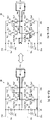
図3に、正のVuoが出力されときのU相電位、O相電位、Vuoの時間変化を示し、図4に、負のVuoが出力されるときのU相電位、O相電位、Vuoの時間変化を示す。また、図5、図6に、それぞれ、図3、図4に示してある電位、電圧の時間変化を実現するために制御ユニット30がインバータ回路20に対して行う制御内容を示す。なお、図3及び図4に示してある電位、電圧の変化パターンは、リアクトルLu、Lo及びLwとコンデンサC3〜C5とにより平滑化されることを考慮していないものである。また、図3、図4及び以下の説明において、U相電位、O相電位、W相電位とは、それぞれ、中性点の電位を基準とした、U端子24u、O端子24o、W端子24wの電位のことである。
FIG. 3 shows changes in U-phase potential, O-phase potential, and Vuo with time when positive Vuo is output, and FIG. 4 shows U-phase potential, O-phase potential, and Vuo when negative Vuo is output. It shows the change over time. Further, FIGS. 5 and 6 show the control contents performed by the
図3及び図4に示してあるように、自立運転中、制御ユニット30は、基本的には、O
相電位が0Vとなり、U相電位が時間変化するように、インバータ回路20を制御する。また、正のVuoを出力する場合、制御ユニット30は、第1コンデンサC1の電圧Vcが負荷40に印加されるモード1(図5(a))と、負荷40に電圧が印加されないモード2(負荷40の両端が中性点に接続されるモード2;図5(b))とで交互に動作するように、インバータ回路20を制御する。負のVuoを出力する場合、制御ユニット30は、第2コンデンサC2の電圧Vcが、負荷40に、正のVuoの出力時とは逆方向に印加されるモード3(図6(a))と、負荷40に電圧が印加されないモード4(負荷40の両端が中性点に接続されるモード4;図6(b))とで交互に動作するように、インバータ回路20を制御する。
As shown in FIGS. 3 and 4, during the self-sustaining operation, the
The
なお、制御ユニット30が行う上記制御は、“モード1の持続時間+モード2の持続時間”が、予め設定されている時間(以下、スイッチング周期と表記する)と一致し、モード1の持続時間/スイッチング周期を、その時点において出力すべきVuo値に応じて変化させる制御である。
In the above control performed by the
また、自立運転中、制御ユニット30は、W相電位が、−U相電位(U相電位の極性を反転させた電位)となるように、インバータ回路20を制御する。
Further, during the self-sustaining operation, the
第1コンデンサC1の端子間電圧と第2コンデンサC2の端子間電圧とが等しい場合、上記制御により、正常な単相3線出力(図2参照)を得ることが出来る。ただし、電力変換装置の利用状況によっては、コンデンサ電圧がアンバランスとなってしまう(第1コンデンサC1の端子間電圧と第2コンデンサC2の端子間電圧とが異なってしまう)場合もある。そして、コンデンサ電圧がアンバランスになると、正常な単相3線出力が得られないことや、インバータ回路20の部品への過電流や過電圧によりインバータ回路20が破損することがあり得る。
When the voltage between terminals of the first capacitor C1 and the voltage between terminals of the second capacitor C2 are equal, a normal single-phase three-wire output (see FIG. 2) can be obtained by the above control. However, the capacitor voltage may be unbalanced (the voltage between the terminals of the first capacitor C1 and the voltage between the terminals of the second capacitor C2 may be different) depending on the usage of the power converter. If the capacitor voltage becomes unbalanced, a normal single-phase three-wire output may not be obtained, or the
そのような不具合が生ずることを抑止するために、本実施形態に係る電力変換装置の制御ユニット30は、自立運転の開始が指示された場合、図7に示した手順の自立運転用制御処理を行うように、構成(プログラミング)されている。なお、自立運転用制御処理のステップS101〜S103の処理は、コンセント用継電器、系統用継電器が共にOFFとされている状態で行われる処理である。
In order to prevent such a problem from occurring, the
すなわち、自立運転の開始が指示されたため、この自立運転用制御処理を開始した制御ユニット30は、まず、電圧センサ31p、31nを用いて第1コンデンサC1の端子間電圧と第2コンデンサC2の端子間電圧とを測定し、測定した端子間電圧間の電圧差を算出する(ステップS101)。
That is, since the start of the self-sustaining operation is instructed, the
次いで、制御ユニット30は、算出した電圧差の絶対値が、第1設定値以下であるか否かを判断する(ステップS102)。ここで、第1設定値とは、上記のような不具合が生ずる恐れがある電圧差として予め設定されている値のことである。
Next, the
制御ユニット30は、電圧差の絶対値が第1設定値以下ではなかった場合(ステップS102;NO)には、ステップS103にて、コンデンサ電圧均衡化処理を行う。
When the absolute value of the voltage difference is not less than or equal to the first set value (step S102; NO), the
コンデンサ電圧均衡化処理は、コンデンサC1、C2間の電圧差が、予め設定されている、第1設定値よりも小さな第2設定値以下となるまで、端子間電圧がより高い方のコンデンサ(C1又はC2)に蓄えられている電力で他方のコンデンサ(C2又はC1)を充電する処理である。 In the capacitor voltage balancing process, the capacitor with the higher terminal voltage (C1) is used until the voltage difference between the capacitors C1 and C2 becomes less than or equal to a preset second set value that is smaller than the first set value. Alternatively, it is a process of charging the other capacitor (C2 or C1) with the electric power stored in C2).
以下、第1コンデンサC1の端子間電圧が第2コンデンサC2の端子間電圧よりも高か
い場合を例に、コンデンサ電圧均衡化処理の内容をより具体的に説明する。
Hereinafter, the content of the capacitor voltage balancing process will be described more specifically, taking as an example the case where the terminal voltage of the first capacitor C1 is higher than the terminal voltage of the second capacitor C2.
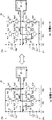
第1コンデンサC1の端子間電圧が第2コンデンサC2の端子間電圧よりも高かった場合、制御ユニット30は、図8及び図9に示した内容のコンデンサ電圧均衡化処理を行う。なお、図8、図9及び後述する図10におけるリアクトルL0、コンデンサC0は、それぞれ、リアクトルLu及びリアクトルLoに相当するインダクタンス成分、コンデンサC3及びコンデンサC4に相当する静電容量成分である。
When the terminal voltage of the first capacitor C1 is higher than the terminal voltage of the second capacitor C2, the
すなわち、第1コンデンサC1の端子間電圧が第2コンデンサC2の端子間電圧よりも高かった場合、制御ユニット30は、コンデンサ電圧均衡化処理を開始して、第1コンデンサC1に放電させた電力でリアクトルL0及びコンデンサC0を充電する放電モード(図8(a))と、リアクトルL0及びコンデンサC0に充電した電力で第2コンデンサC2を充電する充電モード(図8(b))とで交互に動作するようにインバータ回路20を制御する。さらに、図9に示した電流経路で、第1コンデンサC1からの放電と第2コンデンサC2への充電を交互に行う。なお、図8と図9の動作を低周波で入れ替え、それぞれの中の(a)と(b)の切り替えは高周波で行うのが良い。
That is, when the voltage across the terminals of the first capacitor C1 is higher than the voltage across the terminals of the second capacitor C2, the
また、第1コンデンサC1の端子間電圧が第2コンデンサC2の端子間電圧よりも高い場合に、インバータ回路20に図8の(a)、(b)に示した状態を短周期で交互に取らせる制御と、インバータ回路20に図10の(a)、(b)に示した状態を交互に取らせる制御とを繰り返すコンデンサ電圧均衡化処理であって、図8の(a)の状態から図10の(a)の状態へ、又は、図10の(a)の状態から図8の(a)の状態へ移行するコンデンサ電圧均衡化処理が実行されるようにしておいても良い。
When the voltage between terminals of the first capacitor C1 is higher than the voltage between terminals of the second capacitor C2, the
図7に戻って、説明を続ける。
コンデンサ電圧均衡化処理を終えた制御ユニット30は、単相3線出力用制御処理を開始する(ステップS104)。また、電圧差の絶対値が第1設定値以下であった場合(ステップS102;YES)、制御ユニット30は、コンデンサ電圧均衡化処理を行うことなく、単相3線出力用制御処理を開始する(ステップS104)。
Returning to FIG. 7, the description will be continued.
The
単相3線出力用制御処理を開始した制御ユニット30は、まず、コンセント用継電器(自立運転用の100V及び200Vコンセントにインバータ回路20の出力端子を接続するための継電器)をONする。そして、制御ユニット30は、図3〜図6を用いて説明した制御処理に、第1コンデンサC1の端子間電圧と第2コンデンサC2の端子間電圧の電圧差(以下、コンデンサ電圧差と表記する)を小さくするための制御処理を加えた処理を開始する。
The
すなわち、自立運転用の100V、200Vコンセントに接続される機器によっては、自立運転中に、コンデンサ電圧がアンバランスとなってしまう(第1コンデンサC1の端子間電圧と第2コンデンサC2の端子間電圧とが異なってしまう)場合がある。そして、コンデンサ電圧がアンバランスになると、既に説明したように、正常な単相3線出力が得られないことや、インバータ回路20の部品への過電流や過電圧によりインバータ回路20が破損することがあり得る。
That is, depending on the device connected to the 100V or 200V outlet for self-sustaining operation, the capacitor voltage becomes unbalanced during self-sustaining operation (the voltage between the terminals of the first capacitor C1 and the voltage between the terminals of the second capacitor C2). May be different). When the capacitor voltage becomes unbalanced, as described above, normal single-phase three-wire output cannot be obtained, and the
そのような不具合が生ずることを抑止するために、制御ユニット30は、自立運転中に、コンデンサ電圧差が第3設定値を超えた場合には、コンデンサ電圧差を小さくするためのO相電位の制御処理を行うように構成されている。なお、第3設定値とは、予め定められている値のことである。この第3設定値としては、例えば、上記した第1設定値と同じ値を使用することが出来る。
In order to prevent such a problem from occurring, the
具体的には、コンデンサ電圧差が第3設定値を超えた場合、制御ユニット30は、以下の条件を満たすようにO相電位を制御する制御処理を開始する。
Specifically, when the capacitor voltage difference exceeds the third set value, the
条件1:O相電位が正又は負に変化しているときに、端子間電圧が高い方のコンデンサ(C1又はC2)に蓄積された電力が他方のコンデンサに蓄積された電力よりも多く消費される。
条件2:O相電位を、1スイッチング周期内の時間平均値が“0”となるように変化させる。
条件3:O相電位を正又は負となる時間が、コンデンサ電圧差に応じた時間となる。
Condition 1: When the O-phase potential changes to positive or negative, more power is stored in the capacitor (C1 or C2) with a higher terminal voltage than power stored in the other capacitor. It
Condition 2: The O-phase potential is changed so that the time average value within one switching cycle becomes "0".
Condition 3: The time when the O-phase potential becomes positive or negative corresponds to the capacitor voltage difference.
なお、条件3は、O相電位を上下する時間がコンデンサ電圧差に比例するといった条件であっても、O相電位を上下する時間が、コンデンサ電圧差に比例した値と、コンデンサ電圧差の時間積分値とから求められるといった条件であっても、O相電位を上下する時間が、コンデンサ電圧差に比例した値と、コンデンサ電圧差の時間積分値と、コンデンサ電圧差の時間微分値とから求められるといった条件であっても良い。
Note that
条件1が成立すれば、両コンデンサC1及びC2の端子間電圧差を低減することが出来る。また、条件2が成立すれば、Vuo、Vwo、Vuwの波形に悪影響を与えない(各出力波形を歪ませない)ことが出来る。具体的には、正のVuoの出力時を例に説明すると、図11から明らかなように、条件2が成立すれば、Vuoの1スイッチング周期内の積分値が、O相電位を変化させない場合と同じ値となる。従って、条件2が成立すれば、Vuo、Vwo、Vuwの波形に悪影響を与えない(各出力波形を歪ませない)ことが出来る。また、条件3が成立するようにしておけば、両コンデンサC1及びC2の端子間電圧差を、短時間のうちに低減することが可能となる。
If the
そして、インバータ回路20は、条件1〜3を満たした状態で図11に示してあるようにU相電位、O相電位を変化させることができる構成を有している。
Then, the
具体的には、第2コンデンサC2の端子間電圧の方が第1コンデンサC1の端子間電圧よりも高い場合、モード1で動作しているインバータ回路20(図5(a))を、図12に示した電流経路が形成されるモード5で動作させれば、U相電位を変えずに、O相電位を上げること(O相電位を、端子21pの電位(正電位)とすること)が出来る。また、モード2で動作しているインバータ回路20(図5(b))を、図13に示した電流経路が形成されるモード6で動作させれば、U相電位を変えずに、第2コンデンサC2に蓄えられた電力に基づき、O相電位を下げること(O相電位を、端子21nの電位(負電位)とすること)が出来る。
Specifically, when the inter-terminal voltage of the second capacitor C2 is higher than the inter-terminal voltage of the first capacitor C1, the inverter circuit 20 (FIG. 5(a)) operating in the
そのため、第2コンデンサC2の端子間電圧の方が第1コンデンサC1の端子間電圧よりも高い状況下、正のVuoを出力する場合、単相3線出力用制御処理では、図11に示してあるように、インバータ回路20の動作モードが、モード1、5、1、2、6、2といった順に繰り返し変更される。
Therefore, when the positive Vuo is output under the condition that the voltage between terminals of the second capacitor C2 is higher than the voltage between terminals of the first capacitor C1, in the single-phase three-wire output control process, as shown in FIG. As described above, the operation mode of the
正のVuoの出力時に上記制御が行われる場合、単相3線出力用制御処理では、負のVuoの出力時、正/負のVuoの出力時にも同様の制御が行われる。すなわち、上記条件1〜3を満たすように、U端子24uの接続先を、一時的に、中性点から入力端子21p又は21nに変更する制御が行われる。
When the above control is performed when the positive Vuo is output, in the single-phase three-wire output control process, the same control is performed when the negative Vuo is output and when the positive/negative Vuo is output. That is, control is performed to temporarily change the connection destination of the
そして、単相3線出力用制御処理では、コンデンサ電圧差が、第3設定値以下の第4設定値(例えば、第2設定値と同じ値)以下となったときに、通常の制御処理が開始される。 In the single-phase three-wire output control process, the normal control process is performed when the capacitor voltage difference becomes equal to or lower than the fourth set value equal to or lower than the third set value (for example, the same value as the second set value). Be started.
図7に戻って、自立運転用制御処理の残りのステップについて説明する。
上記のような内容の単相3線出力用制御処理を開始した制御ユニット30は、自立運転モードの解除が指示されるのを監視する(ステップS105)。そして、制御ユニット30は、自立運転モードの解除が指示された場合(ステップS105;YES)には、単相3線出力用制御処理を終了する(ステップS106)と共に、この自立運転用制御処理を終了して、三相交流出力用制御処理を開始する。
Returning to FIG. 7, the remaining steps of the self-sustained operation control process will be described.
The
以上、説明したように、本実施形態に係る電力変換装置は、コンデンサ電圧平衡化処理を行う機能(図7、図8等参照)を有している。従って、電力変換装置では、第1コンデンサC1と第2コンデンサC2の端子間電圧に大きな差がある状態で単相3線出力用制御処理が開始されて不具合が生じてしまうことも抑止することが出来る。また、電力変換装置の制御ユニット30は、上記条件1〜3が満たされるように、O相電位を制御する処理を行う機能を有している。そして、当該処理が行われれば、Vuo及びVwo(及びVuw)の波形に悪影響が与えられない形で、端子間電圧が高い方のコンデンサの端子間電圧を他方のコンデンサの端子間電圧に近づくことになる。従って、本実施形態に係る電力変換装置によれば、単相3線出力中に、正常な単相3線出力が得られなくなるといったような不具合が発生し難いことにもなる。
As described above, the power conversion device according to the present embodiment has the function of performing the capacitor voltage balancing process (see FIG. 7, FIG. 8 and the like). Therefore, in the power conversion device, it is possible to prevent the occurrence of a problem by starting the single-phase three-wire output control process in the state where there is a large difference in the voltage between the terminals of the first capacitor C1 and the second capacitor C2. I can. Further, the
《変形例》
上記した実施形態に係る電力変換装置は、各種の変形を行えるものである。例えば、電力変換装置を、単相で系統連系する装置や単相3線出力のみを行う装置に変形することが出来る。また、図14に示してあるように、電力変換装置のインバータ回路20の第1コンデンサC1、第2コンデンサC2に、それぞれ、数百kΩ程度の抵抗25p、抵抗25nを並列接続しておくと共に、上記したコンデンサ電圧均衡化処理の代わりに、コンデンサ電圧差が第2設定値以下となるのを待機する処理が行われるようにしておくことが出来る。また、図15に示してあるように、第1コンデンサC1、第2コンデンサC2に、それぞれ、抵抗26pとスイッチング素子27pとを直列接続した回路、抵抗26nとスイッチング素子27nを直列接続した回路を並列接続しておくと共に、上記したコンデンサ電圧均衡化処理の代わりに、スイッチング素子27p、27nを、一定時間の間だけ、又は、コンデンサ電圧差が規定値以下となるまで、ONする処理が行われるようにしておくことも出来る。
<Modification>
The power conversion device according to the above-described embodiment can be modified in various ways. For example, the power converter can be modified into a single-phase system interconnection device or a device that performs only single-phase three-wire output. Further, as shown in FIG. 14, a
また、電力変換装置を、図16に示した構成を有する装置、すなわち、第1コンデンサC1の両端と第2コンデンサC2の両端とに印加する電圧を個別に制御可能な、2つの直流発電装置35と接続されるDC/DC変換回路10を備えた装置に変形することも出来る。この場合、制御ユニット30を、第1コンデンサC1の端子間電圧と第2コンデンサC2の端子間電圧とが一致するようにDC/DC変換回路10を制御するユニットとしておくだけで、単相3線出力の開始時や実行中に、コンデンサ電圧のアンバランスに起因する不具合が生ずることを抑止できることになる。
Further, the power converter is a device having the configuration shown in FIG. 16, that is, two
また、単相3線出力用制御処理中のO相電位の制御処理は、第1コンデンサC1及び第2コンデンサC2の中の、端子間電圧が高い方のコンデンサに蓄積された電力が他方のコンデンサに蓄積された電力よりも多く消費されるようにO相電位を正負に変化させる処理でありさえすれば、上記したものと具体的な内容が異なる処理であっても良い。従って、例えば、第2コンデンサC2の端子間電圧の方が第1コンデンサC1の端子間電圧よりも高い状況下において正のVuoを出力する場合(図11参照)、インバータ回路20の動作モードが、モード5、1、6、2といった順や、モード1、5、6、2といった順で繰り返し変更されるようにしておいても良い。
Further, in the control processing of the O-phase potential during the control processing for single-phase three-wire output, the power stored in the capacitor having the higher terminal voltage of the first capacitor C1 and the second capacitor C2 is the other capacitor. As long as it is a process of changing the O-phase potential between positive and negative so that it is consumed more than the electric power stored in the above, the process may be different in specific content from the above. Therefore, for example, when a positive Vuo is output in a situation where the voltage across the second capacitor C2 is higher than the voltage across the first capacitor C1 (see FIG. 11), the operation mode of the
また、O相電位を制御する制御処理が常に行われるように、電力変換装置(制御ユニット30)を変形しても良い。ただし、当該制御処理は、第1コンデンサC1の端子間電圧と第2コンデンサC2の端子間電圧がほぼ一致している場合には、不要な処理である。そして、当該制御処理のON/OFFが頻繁に行われるのも好ましいことではないので、制御ユニット30は、上記したように、コンデンサ電圧差が第3設定値を超えている場合にO相電位を制御する処理を開始し、コンデンサ電圧差が第4設定値よりも小さな第4設定値以下となった場合に当該処理を終了する装置として構成しておくことが好ましい。
Further, the power conversion device (control unit 30) may be modified so that the control process for controlling the O-phase potential is always performed. However, the control processing is unnecessary processing when the inter-terminal voltage of the first capacitor C1 and the inter-terminal voltage of the second capacitor C2 are substantially the same. Since it is not preferable that the control process is frequently turned ON/OFF, the
また、制御ユニット20を、単相3線出力用制御処理の実行中に、コンデンサ電圧差が過度に大きくなった場合、単相3線出力用制御処理を中止すると共にコンセント用継電器をOFFし、コンデンサ電圧均衡化処理によりコンデンサ電圧差を小さくしてから、単相3線出力を再開するユニットに変形しておいても良い。さらに、インバータ回路20の具体的な構成(回路構成、使用されている素子)が上記したものとは異なっていても良いことや、自立運転時の電力の出力先が自立運転用のコンセントではなくても良いことなどは、当然のことである。
In addition, when the capacitor voltage difference becomes excessively large during execution of the control processing for the single-phase three-wire output in the
10 DC/DC変換回路
11n、11p 入力端子
20 インバータ回路
21n、21p 入力端子
22 分圧回路
23o O相用レグ
23u U相用レグ
23w W相用レグ
24o O端子
24u U端子
24w W端子
27n、27p スイッチング素子
30 制御ユニット
31n、41p 電圧センサ
35 直流発電装置
40 負荷
C1〜C5 コンデンサ
Du1〜Du6、Do1〜Do6、Dw1〜Dw6 ダイオード
Lu、Lo、Lw リアクトル
Su1〜Su4、So1〜So4、Sw1〜Sw6 スイッチング素子
10 DC/
Claims (4)
前記インバータ回路に対して、前記第1出力端子及び前記第2出力端子間から第1の交流を出力させると共に前記第3出力端子及び前記第2出力端子間から前記第1の交流の極性を反転した第2の交流を出力させるための単相3線出力用制御処理を実行可能な制御装置と、
を含み、
前記制御装置は、前記単相3線出力用制御処理の開始が指示されたときに、前記第1コンデンサの端子間電圧と前記第2コンデンサの端子間電圧との間の電圧差が所定の閾値以下ではなかった場合には、前記電圧差を低減するためのコンデンサ電圧均衡化処理を行ってから、前記単相3線出力用制御処理を開始し、
前記コンデンサ電圧均衡化処理は、前記第1コンデンサ及び前記第2コンデンサのうちの端子間電圧が高い方のコンデンサに蓄えられている電力のうちの少なくとも一部を第3コンデンサに充電し、前記第3コンデンサに充電された電力が前記第1コンデンサ及び前記第2コンデンサのうちの端子間電圧の低い方のコンデンサに充電されるように前記インバータ回路を制御する処理を含む、
ことを特徴とする電力変換装置。 A neutral point clamp system including a first capacitor and a second capacitor connected in series for dividing the input DC voltage into half, a plurality of switching elements, and first to third output terminals. An inverter circuit,
The inverter circuit is caused to output a first alternating current between the first output terminal and the second output terminal, and the polarity of the first alternating current is inverted between the third output terminal and the second output terminal. A control device capable of executing a single-phase three-wire output control process for outputting the second alternating current,
Including,
The control device, when instructed to start the single-phase three-wire output control process, determines that the voltage difference between the terminal voltage of the first capacitor and the terminal voltage of the second capacitor is a predetermined threshold value. If not, the capacitor voltage balancing process for reducing the voltage difference is performed, and then the single-phase three-wire output control process is started .
In the capacitor voltage balancing process, at least a part of electric power stored in one of the first capacitor and the second capacitor having a higher inter-terminal voltage is charged in the third capacitor, and the third capacitor is charged. A process for controlling the inverter circuit so that the electric power charged in the three capacitors is charged in the one of the first capacitor and the second capacitor having a lower inter-terminal voltage,
A power converter characterized by the above.
ことを特徴とする請求項1に記載の電力変換装置。 The control device starts the single-phase three-wire output control process without performing the capacitor voltage balancing process when the voltage difference is equal to or less than the threshold value. The power converter according to 1.
前記コンデンサ電圧均衡化処理が、前記第1コンデンサの端子間電圧と前記第2コンデンサの端子間電圧との間の電圧差が、前記閾値以下の第2閾値以下となるまで待機する処理である
ことを特徴とする請求項1又は2に記載の電力変換装置。 The inverter circuit is a circuit including a first resistor connected in parallel to both ends of the first capacitor, and a second resistor connected in parallel to both ends of the second capacitor,
The capacitor voltage balancing process is a process of waiting until the voltage difference between the terminal voltage of the first capacitor and the terminal voltage of the second capacitor becomes equal to or less than a second threshold value that is equal to or less than the threshold value. The power conversion device according to claim 1 or 2.
前記コンデンサ電圧均衡化処理が、前記第1スイッチング素子及び前記第2スイッチング素子を所定時間の間だけONする処理である
ことを特徴とする請求項1又は2に記載の電力変換装置。 In the inverter circuit, a circuit in which a first resistor and a first switching element are connected in series is connected in parallel to both ends of the first capacitor, and a circuit in which a second resistor and a second switching element are connected in series is the second capacitor. Is a circuit connected in parallel at both ends of
The power conversion device according to claim 1 or 2, wherein the capacitor voltage balancing process is a process of turning on the first switching element and the second switching element for a predetermined time.
Priority Applications (2)
| Application Number | Priority Date | Filing Date | Title |
|---|---|---|---|
| JP2016138517A JP6711185B2 (en) | 2016-07-13 | 2016-07-13 | Power converter |
| US15/628,989 US20180019684A1 (en) | 2016-07-13 | 2017-06-21 | Power converter |
Applications Claiming Priority (1)
| Application Number | Priority Date | Filing Date | Title |
|---|---|---|---|
| JP2016138517A JP6711185B2 (en) | 2016-07-13 | 2016-07-13 | Power converter |
Publications (3)
| Publication Number | Publication Date |
|---|---|
| JP2018011420A JP2018011420A (en) | 2018-01-18 |
| JP2018011420A5 JP2018011420A5 (en) | 2019-03-22 |
| JP6711185B2 true JP6711185B2 (en) | 2020-06-17 |
Family
ID=60942249
Family Applications (1)
| Application Number | Title | Priority Date | Filing Date |
|---|---|---|---|
| JP2016138517A Active JP6711185B2 (en) | 2016-07-13 | 2016-07-13 | Power converter |
Country Status (2)
| Country | Link |
|---|---|
| US (1) | US20180019684A1 (en) |
| JP (1) | JP6711185B2 (en) |
Families Citing this family (5)
| Publication number | Priority date | Publication date | Assignee | Title |
|---|---|---|---|---|
| CN108270366A (en) * | 2016-12-30 | 2018-07-10 | 艾思玛新能源技术(江苏)有限公司 | A kind of modulator approach and device based on three-phase neutral point clamp type inverter |
| DE102018118068A1 (en) * | 2018-07-26 | 2020-01-30 | Ebm-Papst Mulfingen Gmbh & Co. Kg | Circuit arrangement for DC link balancing |
| CN109149987A (en) * | 2018-08-08 | 2019-01-04 | 中国电力科学研究院有限公司 | A kind of production method of the three level energy accumulation current converters based on A-NPC topology |
| GB201815301D0 (en) * | 2018-09-20 | 2018-11-07 | Rolls Royce | Converter |
| JP7126133B2 (en) * | 2018-11-29 | 2022-08-26 | パナソニックIpマネジメント株式会社 | power converter |
Family Cites Families (9)
| Publication number | Priority date | Publication date | Assignee | Title |
|---|---|---|---|---|
| JPH09331684A (en) * | 1996-06-11 | 1997-12-22 | Fuji Electric Co Ltd | Non-insulated type uninterruptible power-supply unit |
| JP4494562B2 (en) * | 1999-09-28 | 2010-06-30 | 株式会社ダイヘン | Power converter for photovoltaic power generation |
| JP2007097355A (en) * | 2005-09-30 | 2007-04-12 | Sanyo Electric Co Ltd | Inverter circuit |
| TWI346441B (en) * | 2006-11-10 | 2011-08-01 | Delta Electronics Inc | Three-level ac generating circuit and control method thereof |
| JP5110960B2 (en) * | 2007-05-15 | 2012-12-26 | 新電元工業株式会社 | Grid-connected inverter device |
| JP6087531B2 (en) * | 2012-08-06 | 2017-03-01 | 三菱電機株式会社 | Power converter |
| JP6103874B2 (en) * | 2012-10-12 | 2017-03-29 | 株式会社日立情報通信エンジニアリング | Power supply device and its operation method |
| JP6048928B2 (en) * | 2012-10-23 | 2016-12-21 | パナソニックIpマネジメント株式会社 | Power converter |
| JP6087238B2 (en) * | 2013-07-26 | 2017-03-01 | 株式会社日立情報通信エンジニアリング | Power supply device and its operation method |
-
2016
- 2016-07-13 JP JP2016138517A patent/JP6711185B2/en active Active
-
2017
- 2017-06-21 US US15/628,989 patent/US20180019684A1/en not_active Abandoned
Also Published As
| Publication number | Publication date |
|---|---|
| US20180019684A1 (en) | 2018-01-18 |
| JP2018011420A (en) | 2018-01-18 |
Similar Documents
| Publication | Publication Date | Title |
|---|---|---|
| JP6711185B2 (en) | Power converter | |
| JP5701279B2 (en) | Charge control device, battery system, and charge control method | |
| JP4512145B2 (en) | Motor control device | |
| JP5097828B2 (en) | Power converter | |
| JP6048928B2 (en) | Power converter | |
| CN107155383B (en) | Uninterruptible power supply device | |
| JP6658369B2 (en) | Power converter | |
| JP6681476B2 (en) | Power converter and power converter control method | |
| JP6087238B2 (en) | Power supply device and its operation method | |
| NZ744394A (en) | Electric vehicle power distribution system | |
| JP6087531B2 (en) | Power converter | |
| CN103378736B (en) | Power supply unit and method of operation thereof and comprise the solar power system of power supply unit | |
| JP5411000B2 (en) | Power converter | |
| CN107750424A (en) | Power inverter and the method for controlling the power inverter | |
| CN117811090A (en) | System and method for increasing reliability and useful life of Photovoltaic (PV) modules | |
| JP2018019481A (en) | Power conversion device | |
| JP5919483B2 (en) | Grid interconnection device | |
| JP5398162B2 (en) | Grid-connected inverter device | |
| WO2010103600A1 (en) | Power conversion apparatus | |
| Ounejjar et al. | New nine-level inverter with self balancing of capacitors voltages | |
| JP2017189053A (en) | Motor device | |
| JP2009247185A (en) | System-cooperative inverter and its self-sustaining operation method | |
| KR20120096089A (en) | Groundable dc/dc converter | |
| JP2011193704A (en) | Dc-ac power converter | |
| JP6470832B2 (en) | Power converter and initial charging method thereof |
Legal Events
| Date | Code | Title | Description |
|---|---|---|---|
| A521 | Request for written amendment filed |
Free format text: JAPANESE INTERMEDIATE CODE: A523 Effective date: 20190207 |
|
| A621 | Written request for application examination |
Free format text: JAPANESE INTERMEDIATE CODE: A621 Effective date: 20190207 |
|
| A977 | Report on retrieval |
Free format text: JAPANESE INTERMEDIATE CODE: A971007 Effective date: 20191213 |
|
| A131 | Notification of reasons for refusal |
Free format text: JAPANESE INTERMEDIATE CODE: A131 Effective date: 20200107 |
|
| A521 | Request for written amendment filed |
Free format text: JAPANESE INTERMEDIATE CODE: A523 Effective date: 20200221 |
|
| TRDD | Decision of grant or rejection written | ||
| A01 | Written decision to grant a patent or to grant a registration (utility model) |
Free format text: JAPANESE INTERMEDIATE CODE: A01 Effective date: 20200428 |
|
| A61 | First payment of annual fees (during grant procedure) |
Free format text: JAPANESE INTERMEDIATE CODE: A61 Effective date: 20200511 |
|
| R150 | Certificate of patent or registration of utility model |
Ref document number: 6711185 Country of ref document: JP Free format text: JAPANESE INTERMEDIATE CODE: R150 |
|
| R250 | Receipt of annual fees |
Free format text: JAPANESE INTERMEDIATE CODE: R250 |